
Layer-dependent spin texture and origins of Rashba splitting quenching in the 2D CsPbI3 perovskite
Safieh
Nazari
 *a and
Yavar
T. Azar
b
*a and
Yavar
T. Azar
b
aPhysics and Accelerators Research School, Nuclear Science and Technology Research Institute, Tehran, Iran. E-mail: nazari.s@gmail.com
bPhysics and Accelerators Research School, AEOI, Tehran, Iran
First published on 23rd April 2024
Abstract
The spin–orbit coupling in inorganic perovskite materials containing heavy elements causes interesting electronic characteristics such as Rashba and Dresselhaus effects. Several studies have reported significant band splitting in the presence of asymmetry, while the impacts of the external field strength, surface termination on the electronic structure still need to be resolved. In the current study, a systematic relation between the external parameters and the band splitting in CsPbI3 slabs is clarified through first-principles calculations. Here, we examine the band splitting and spin patterns of CsPbI3 slabs exposed to an external electric field ranging from zero to hundreds of kV cm−1. Our results indicate apparent non-linear behavior of the Rashba coefficient along with a turning point for the band splitting for a definite external field. Here, the origin of this quench in the band splitting is explained in terms of spatial localization of the wave functions and clear change in their center of charge going from low to high electric fields. The findings not only explain the origin of quenching band splitting but also reveal the external field's significance in the spin texture and recombination rate of 2D perovskites. The current research outcome paves the way for atomic scale engineering of perovskite materials for a wide range of applications.
1 Introduction
The last decade has witnessed a rapid surge of interest in developing hybrid organic/inorganic perovskites (HOPs). Tremendous research efforts on the compositional design and mechanisms behind the efficient operation of these materials has extended their application in photovoltaics, optoelectronics, field-effect transistors, memristors, and more.1–4 After the astonishing leap in efficiency of perovskite-based photovoltaic devices, numerous suggestions have been made for their application in other fields. In particular, having heavy elements with effective spin–orbit coupling (SOC) makes them potential candidates for spintronics applications.5 Theoretical and experimental research has been conducted over the last few years and has revealed the Rashba-type6 band splitting in hybrid organic/inorganic halide perovskites through symmetry breaking.7 The giant spin–orbit coupling (SOC) in this family is accepted as the main origin of Rashba-like splittings in their band structures.8,9From a theoretical point of view, structural asymmetry plays a central role in the appearance of spin-polarization. This asymmetry can be rooted in the external field, interfacial built-in field, and geometrical distortion.10 Shanavas et al. showed that perovskite structures in the presence of an applied electric field are ideal systems for tunable Rashba splitting.11 In addition, Myung et al. declared that the inversion symmetry breaking field at the interfaces between perovskite and substrate, exhibits remarkable band splitting.12 Chen et al. studied the influence of an external electric field on bilayer CsPbBr3, indicating a significant different between the Rashba coefficient attributed to different terminations.13 A similar Rashba effect has been observed for other 2D perovskites in the presence of an electric field. 2D orthorhombic RbSnI3 as a prominent example, exhibits the largest Rashba parameter among all members of this family.14
Despite all the above-mentioned efforts on the characterization of spin-polarization as a function of external variables, the characteristic SOC-induced band splitting in 2D CsPbI3 has yet to be dealt with in depth. In this context, the current study employing an ab initio approach calls into question the geometry- and field-induced modifications in the band structure and the spin texture of 2D films. Our results demonstrate the complicated behavior of the band splitting and the spin texture through changes in the external electric field. Deepening our understanding of what is happening in these systems could be the cornerstone for the purposeful design of these materials for various applications.
2 Computational materials
All calculations were carried out using the quantum-ESPRESSO15,16 DFT package with the Perdew–Burke–Ernzerhof (PBE) version of the generalized gradient approximation (GGA).17 The electronic wave functions are expanded onto a plane-wave basis set with the kinetic energy cut-off of 35 Ry. Fully relativistic pseudopotentials are used for Pb 5d6s6p, I 5s5p, and Cs 6s.The CsI-terminated and PbI2-terminated slabs are considered in (001), as a function of thickness n, which denotes the number of octahedrals, and about 18 Å vacuum between consecutive images to model perovskite surfaces. The 6 × 6 × 1 Monkhorst–Pack grids are used for Brillouin-zone (BZ) sampling for the optimization and self-consistent field (SCF) calculations. The atomic positions are relaxed until the residual forces on each atom become less than 0.001 Ry Bohr−1.
Utilizing the various implementations of DFT can create small changes in the simulation results. While Quantum espresso benefits from the accuracy of the plane-wave basis set, the methods based on the linear combination of atomic orbitals (LCAO) have significant savings in the cost of calculations. In this work, the recent development of the SOC in Siesta package18–20 has been employed to examine the sensitivity of band-splitting and spin-texture results to the level of theory.
3 Results and discussion
3.1 Interplay of the external field and SOC-induced band splitting
In the presence of a spin–orbit coupling system the Hamiltonian at the first approximation can be written as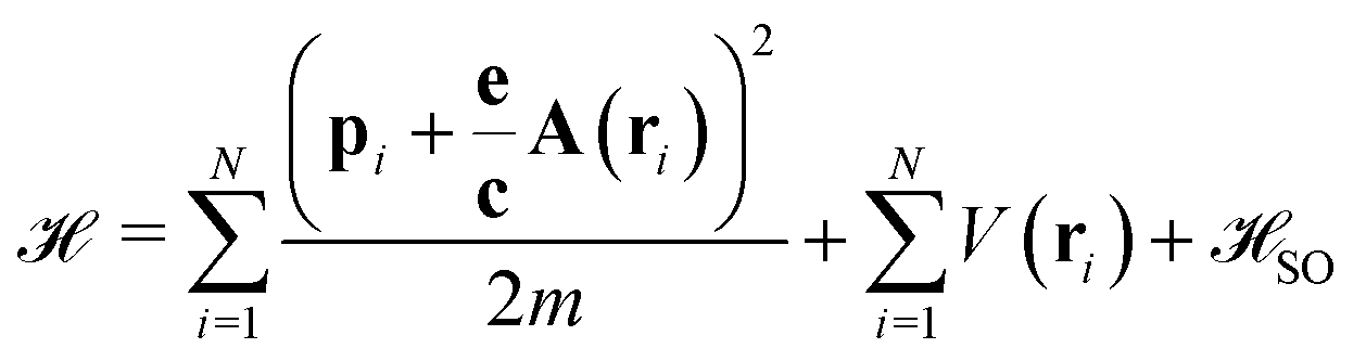 | (1) |
 which adds the SOC contribution to the unperturbed Hamiltonian
  ,
,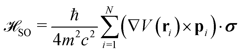 | (2) |
![[3 with combining macron]](https://www.rsc.org/images/entities/char_0033_0304.gif) m (no. 221) space group with five atoms in the primitive unit cell. Cs, Pb and I atoms set up in Wyckoff positions, a, b, c and mm, mm and 4/mm·m site symmetries, respectively. Truncation of the bulk structure perpendicular to the c-axis with two possible CsI- and PbI2 terminations yields two 2D slabs with P4mm (no. 99) space group. For this slab model with high symmetry C4v point group, above perturbation reduces to the so-called Rashba Hamiltonian:21
m (no. 221) space group with five atoms in the primitive unit cell. Cs, Pb and I atoms set up in Wyckoff positions, a, b, c and mm, mm and 4/mm·m site symmetries, respectively. Truncation of the bulk structure perpendicular to the c-axis with two possible CsI- and PbI2 terminations yields two 2D slabs with P4mm (no. 99) space group. For this slab model with high symmetry C4v point group, above perturbation reduces to the so-called Rashba Hamiltonian:21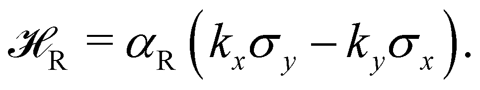 | (3) |
The Rashba parameter (αR) can be calculated from band splitting at the close vicinity of the special k-point
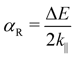 | (4) |
 | ||
| Fig. 1 Inner and outer branches of the band are depicted in brown and gold after Rashba-splitting, circular arrows show the spin texture for each branch. | ||
In this work, we investigate the electronic structure of two different CsPbI3 terminations in the presence of the external electric field. Applying the external field significantly affects the electronic structure of the systems, in particular SOC-induced band splittings. In this regard, in the remainder of this article the effect of the external electric field on the charge distribution, the band splitting, and the spin pattern are explored for two different terminations.
3.2 Charge polarization in the external field
Charge redistribution and potential variation are the two most intuitive changes that can be observed in systems after applying an external field, and have a significant impact on the electronic structure. Therefore, the first part of our results address the slab’s polarization in detail. The charge and potential for both slabs are calculated before and after applying the external electric field and are illustrated in Fig. 2, for thickness n = 3. As can be seen, there is a clear charge transfer along with electric potential gradient. More in depth exploration of the charge difference pattern indicates stronger polarization effects at the space near the atomic centers. | ||
| Fig. 2 The structure of a CsI-terminated slab with atomic layers labeled from the top to bottom (a), and 2-dimensional representation of the field-induced charge displacement along the Y–Z plane, yellowish and darkish green regions represent charge accumulation and depletion regions, respectively (b). 2D-Representation of the field induced changes in the electrostatic potential along the Y–Z plane (c). | ||
While one can expect unequal changes for different atomic layers in the z-direction, regarding the periodic geometry of these slabs in the xy-plane there is no significant redistribution over the xy-plane. Hence, the planar averaged charge can be calculated as follows:
 | (5) |
In a same way one can calculate the planar average for the electrostatic potential before and after the external field application to gain more insight into the system response. For instance, considering thickness n = 3, the averaged induced charge, Δ![[small rho, Greek, macron]](https://www.rsc.org/images/entities/i_char_e0d1.gif) (z) = E(z) − E=0(z), is calculated and depicted in Fig. 3 for both CsI- and PbI2 terminated slabs. The successive peaks in the ρ(z) plots are attributable to the consecutive atomic layers, …/PbI2/CsI/PbI2/…, and valleys between these peaks are indicative of interstitial space between the atomic layers. As seen in both cases, surface layers are more polarized compared to the interior atomic layers. Also, comparing the polarization of individual atomic layers in each case demonstrates a higher polarization of the PbI2 layers compared with the CsI ones.
(z) = E(z) − E=0(z), is calculated and depicted in Fig. 3 for both CsI- and PbI2 terminated slabs. The successive peaks in the ρ(z) plots are attributable to the consecutive atomic layers, …/PbI2/CsI/PbI2/…, and valleys between these peaks are indicative of interstitial space between the atomic layers. As seen in both cases, surface layers are more polarized compared to the interior atomic layers. Also, comparing the polarization of individual atomic layers in each case demonstrates a higher polarization of the PbI2 layers compared with the CsI ones.
 | ||
| Fig. 3 The averaged induced charge densities generated by a range of external electric fields (0.0005–0.002 a.u.) along the z axis are shown for CsI-terminated (top), and PbI2-terminated (bottom) slabs. | ||
3.3 The electronic structure
Due to heavy elements, such as lead and iodine in the perovskite compositions, relativistic effects play an essential role in their electronic structure. The band gap narrowing caused by SOC correction was shown by Umari et al.22,23 Beyond this vertical shift, the SOC accompanied by an inversion asymmetry might give rise to a more sophisticated spin-splitting in a halide perovskite. In the following, to elucidate the splitting of the energy level for the two different slabs, with various thicknesses, the band structure calculations were done, taking SOC into account. As illustrated in Fig. 4 both the orbital contributions and the spin texture pattern can be different with regard to the type of termination and thickness of slabs, as we will see in next sections. | ||
| Fig. 4 The band structure of the CsI- and PbI2-terminated slabs for n = 3 (upper panel), and the corresponding spin textures (lower panel). | ||
A glance at the two band structures reveals the different responses of CsI- and PbI2-terminated slabs to the  As shown in Fig. 5, after applying the external field, the band gap of the two slabs decreases at each thickness, with increasing electric field from
  to
to  , a dissimilar response to other electronic behaviors. The conduction and valence bands were split into two subbands. The spin for the two subbands is different: for CsI-terminated the spin up and down are parallel, while the one for the PbI2-terminated slab are in the opposite orientations, although for the subband of the neighbor bands, they can be parallel or antiparallel. From the excitonic transitions point of view, the spin orientation in the upper subband of VBM and the lower subband of CBM has a determining role in the electron–hole (e–h) recombination rate. While the parallel spin orientation in these two subbands facilitates the e–h recombination, their anti-parallel orientation might make a spin-forbidden transition.24 Conducting a more in-depth analysis of the band splitting as a function of external field strength, the band separation along with Rashba parameters are calculated, and obtained for each slab as shown in Fig. 5.
 | ||
| Fig. 5 The energy band-gap as a function of external field, for CsI- and PbI2 terminated slabs with n = 2, 3, 4 thickness. | ||
As indicated in Fig. 6, for n = 2 the two types of termination show a semi-linear increase in the band splitting and Rashba parameters, however, this behavior is not consistent for the other thicknesses, n = 3 and n = 4. In these cases, maybe there is a turning point in the VBM or CBM, in which the Rashba parameters first decrease and then start to increase, or vice versa. As a result, the Rashba parameter must depend on the type of termination and thickness of slab. These results are in agreement with that of Yin et al. who showed that the Rashba splitting for the two types of termination of MAPbI3 is strongly dependant on the number of atomic layers.25 In addition, our results show that for the CsI-terminated slab at  αv almost converges for 2L, but for greater thicknesses, this behavior does not follow.
 | ||
| Fig. 6 Changes in Rashba parameters as a function of external field, for the valence and conduction bands in CsI- and PbI2 terminated slabs with n = 2, 3, 4 thickness. | ||
In cases where there is a turning point, for instance in CB bands from 3L of the PbI2-terminated slab, raising the external electric field toward the point turning causes the gradual elimination of band splitting. Exploring the projection of valence band states over the atomic orbitals reveals that from the LCAO viewpoint, wave function corresponding to the valence band can be written as: ψv,k=M = c1ϕ1 + c2ϕ2 + c3ϕ3 + c4ϕ4 where ϕi is the iodine atomic p-orbital corresponding to the i-th layer.
To gain more insight into these contributions, the isovalue surface of the |ψn(r)|2 for the VBM and CBM wave functions at the extremum energies, are visualized in Fig. 7, the isosurface value is ≃0.0011 A g−3. As is clear from Fig. 7, at  two interior PbI2 layers provide the main contribution. Increasing the electric field in the z direction causes an effective potential gradient which shifts the atomic layers contribution in the VBM and CBM in the same direction. At a definite threshold field, this potential shift changes the order of the layers contribution to the valence band, and the outermost layer becomes the most dominant one. This gradual transfer of valence band wave function from interior to border layers, can explain the decline in the band splitting. Similar evidence for this effect is reported by Wang et al. for Ge quantum dots. According to these results there is a critical electric field whereby beyond this value, the Rashba parameter decreases.26
 | ||
Fig. 7 Isosurface density of the valence and conduction edge wave function for  . Pb, I and Cs atoms are represented by the dark gray, purple and phosphor green, respectively. . Pb, I and Cs atoms are represented by the dark gray, purple and phosphor green, respectively. | ||
Our results indicate that changes in the localization of the wave function quenches the splitting in larger fields and causes a significant drop in the Rashba parameter. To gain better insight into the environment effect, the planar averaged potentials, ![[V with combining macron]](https://www.rsc.org/images/entities/i_char_0056_0304.gif) (z), are calculated and visualized in Fig. 8. As is expected, increasing the external field leads to an effective shift in the extremum points of (z).
(z), are calculated and visualized in Fig. 8. As is expected, increasing the external field leads to an effective shift in the extremum points of (z).
 | ||
| Fig. 8 Planar average of potential in the xy plane for the external fields: 0.0, 0.001, and 0.002 atomic unit. | ||
It should be noted that the VBM wave function can be described as a linear combination of four atomic orbitals, spatially localized on the potential wells corresponding to the PbI2 layers. The relative displacement of these potential wells changes the contribution of the different layers in the VBM wave function and the energetically uppermost well has the dominant contribution. Application of the external field up to 0.001 a.u. shifts the well minima, however an inner layer still has the highest level of the potential minimum. Going from  a.u., changes the potential wells in a way whereby the outermost layer has the higher potential, and consequently the wave function shows more localization on the slab surface (see Fig. 7).
In summary, for a spatially fixed wave function, αR changes linearly versus growth of the external field, analogous with the free electron gas. In contrast, if the electric field affects the spatial localization of the wave function significantly, changes in the potential gradient term (∇ϕ) in the Rashba Hamiltonian became more complicated and the Rashba parameter does not follow a linear increase with the applied field.
3.4 Spin-texture
The relative orientation of the spin vectors corresponding to the conduction and valence bands are determining factors in electron–hole recombination time. To visualize the spin texture for CBM/VBM, the expectation values of the spin were calculated in the close neighborhood of extremum points of CBM/VBM bands. In this regard, for all given Kohn–Sham wave functions,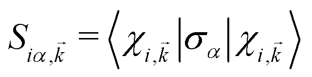 are calculated, where σα (α = 1, 2, 3) are the Pauli matrix components, and
  is i-th spinor eigen-function. The reciprocal lattice was sampled with M-centered 8 × 8 mesh, and
 ![[k with combining right harpoon above (vector)]](https://www.rsc.org/images/entities/i_char_006b_20d1.gif) stands for the wave-vector corresponding to each point. The spin texture of the two types of termination for different thickness n is calculated in a definite range of electric field and obtained patterns, depicted in Fig. 9–11.
stands for the wave-vector corresponding to each point. The spin texture of the two types of termination for different thickness n is calculated in a definite range of electric field and obtained patterns, depicted in Fig. 9–11.
 | ||
Fig. 9 Spin textures of spin vectors  are calculated, where σα (α = 1, 2, 3) are the Pauli matrix components, and are calculated, where σα (α = 1, 2, 3) are the Pauli matrix components, and  is the i-th spinor eigen-function in the kx–ky plane for CsI (left)- and PbI2 (right) terminated with thickness n = 2 in weak and strong external fields. is the i-th spinor eigen-function in the kx–ky plane for CsI (left)- and PbI2 (right) terminated with thickness n = 2 in weak and strong external fields. | ||
 | ||
Fig. 10 Spin texture of spin vectors  are calculated, where σα (α = 1, 2, 3) are the Pauli matrix components, and are calculated, where σα (α = 1, 2, 3) are the Pauli matrix components, and  is the i-th spinor eigen-function in the kx–ky plane for CsI (left)- and PbI2 (right) terminated with thickness n = 3 in weak and strong external fields. is the i-th spinor eigen-function in the kx–ky plane for CsI (left)- and PbI2 (right) terminated with thickness n = 3 in weak and strong external fields. | ||
 | ||
Fig. 11 Spin texture of spin vectors  are calculated, where σα (α = 1, 2, 3) are the Pauli matrix components, and are calculated, where σα (α = 1, 2, 3) are the Pauli matrix components, and  is the i-th spinor eigen-function in the kx–ky plane for CsI (left)- and PbI2 (right) (right) terminated with thickness n = 4 in weak and strong external fields. is the i-th spinor eigen-function in the kx–ky plane for CsI (left)- and PbI2 (right) (right) terminated with thickness n = 4 in weak and strong external fields. | ||
As shown, the spin texture can be controlled with an external electric field, although the response of the two types of terminated slabs in various field ranges is not the same. For each slab, a lack of inversion symmetry and asymmetry charge distribution gives rise to a negative surface dipole or an internal electric field that can compensate by applying an external electric field. However, there are some points worth mentioning: first, as shown, in general, each type of termination has three spin patterns, in which spin up and down can be parallel in the clockwise or anti-clockwise, and/or be in anti-parallel directions. Nevertheless, there is an exception to this rule, the CsI-terminated slab for n = 4, has a single spin pattern throughout the range of the electric field, the anti-clockwise direction. In other cases, however, generally, there is a critical value of the external electric field beyond which leads to rotating the CBM or VBM spin vectors toward the other in the same direction or one of them travels in the opposite direction. For instance, the CsI-terminated slab with thickness n = 3, when the surface is exposed to the electric field, the pattern remains unchanged almost up to 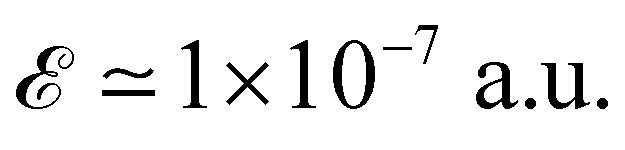 (equivalent to 5.14 × 10⁻¹ kV cm−1), but increases with further electric field increase up to
 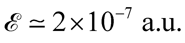 (equivalent to 1.028 kV cm−1); this pattern remains unchanged almost up to
  (equivalent to 2.57 kV cm−1), however, beyond this, the electric field leads to rotation of the CBM vector toward the VBM vector. This pattern maintains up to the higher fields, in this work almost up to
  (equivalent to 2.056 × 10+4 kV cm−1) has been tested. A similar argument holds for the other slabs.
As discussed above, in various ranges of the electric fields, the surface structures have different spin textures. It means that for the two types of termination, the electric field can act as a tuning parameter for the recombination rate of the charge carriers. For instance, there are ranges of the electric field that causes parallel orientation of the VBM and CBM spin vectors, which in turn leads to spin-allowed transitions. In contrast, the anti-parallel orientation of spin vectors gives rise to spin-forbidden transitions. Switching between the spin-allowed and forbidden states in the external field tuning is intriguing, in both optoelectronic and spintronic devices. Recently, it was established that all-inorganic perovskites under keV cm−1 (∼1 × 10⁻⁷ a.u.) electric field show high piezoelectricity.27 The obtained results in the present work indicate that such a small field can also be the determining factor in the spintronic properties of the system. Therefore the correlation between spintronic and piezoelectric parameters could be investigated in the future. Finally, the last point that should be considered is the influence of the presence of the turning points on the spin pattern. The results show that at the turning point for n = 2, 3 (2L and 3L) the spin pattern maintains itself up to a high electric field. But this issue about the PbI2 terminated slab for n = 4 (4L) is completely different. As shown in Fig. 12, the turning point plays a main role, and the VBM spin vector starts to rotate until they are in opposite directions to each other.
 | ||
Fig. 12 Spin texture of spin vectors 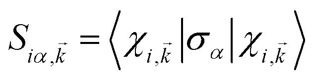 are calculated, where σα (α = 1, 2, 3) are the Pauli matrix components, and are calculated, where σα (α = 1, 2, 3) are the Pauli matrix components, and  is the i-th spinor eigen-function in the kx−ky plane for the PbI2 terminated with thickness n = 4 around the turning point and higher, values. is the i-th spinor eigen-function in the kx−ky plane for the PbI2 terminated with thickness n = 4 around the turning point and higher, values. | ||
4 Summary and outlook
The present study was designed to determine the electronic structure for the two types of termination of the CsPbI3 perovskite slabs in the presence of external fields. This study identified a tight correlation between the environmental variables and the SOC-induced band splitting of the CBM/VBM. In this regard, the electric field can be employed to tune the Rashba parameters and the spin texture for these systems. This can raise two distinct electron–hole recombination rates and spintronic responses for these two different terminations, which is determining factor for their optoelectronic applications. The non-linear behavior of the Rashba coefficient versus the electric field is concluded and explained in terms of changes in spatial localization of the wave functions corresponding to the CBM and VBM. The present findings confirm the critical rule of built-in or external fields in tuning the spintronic properties of perovskite slabs. In summary, the band splitting quenching due to the change in the localization of wave function and the change of the spin texture behavior going from weak to strong fields, were two aspects not considered enough until the current work. The insights gained from this study may assist in tuning band splitting and designing spintronic related devices based on perovskite materials.Conflicts of interest
There are no conflicts to declare.References
- G. Grancini and M. K. Nazeeruddin, Nat. Rev. Mater., 2019, 4, 4–22 CrossRef CAS.
- P. Schulz, D. Cahen and A. Kahn, Chem. Rev., 2019, 119, 3349–3417 CrossRef CAS PubMed.
- C. R. Kagan, D. B. Mitzi and C. D. Dimitrakopoulos, Science, 1999, 286, 945–947 CrossRef CAS PubMed.
- G. Lin, Y. Lin, R. Cui, H. Huang, X. Guo, C. Li, J. Dong, X. Guo and B. Sun, J. Mater. Chem. C, 2015, 3, 10793–10798 RSC.
- K. Liao, X. Hu, Y. Cheng, Z. Yu, Y. Xue, Y. Chen and Q. Gong, Adv. Opt. Mater., 2019, 7, 1900350 CrossRef.
- E. I. Rashba, Soviet Phys., Solid State, 1960, 2, 1109–1122 Search PubMed.
- L. Leppert, S. E. Reyes-Lillo and J. B. Neaton, J. Phys. Chem. Lett., 2016, 7, 3683–3689 CrossRef CAS PubMed.
- J. Even, L. Pedesseau, J.-M. Jancu and C. Katan, J. Phys. Chem. Lett., 2013, 4, 2999–3005 CrossRef CAS.
- J. Even, L. Pedesseau, J.-M. Jancu and C. Katan, Phys. Status Solidi RRL, 2014, 8, 31–35 CrossRef CAS.
- X. Zhang, Q. Liu, J.-W. Luo, A. J. Freeman and A. Zunger, Nat. Phys., 2014, 10, 387–393 Search PubMed.
- K. Shanavas and S. Satpathy, Phys. Rev. Lett., 2014, 112, 086802 CrossRef.
- C. W. Myung, S. Javaid, K. S. Kim and G. Lee, ACS Energy Lett., 2018, 3, 1294–1300 CrossRef CAS.
- X. Chen, L. Liu and D. Shen, J. Phys.: Condens. Matter, 2018, 30, 265501 CrossRef PubMed.
- J. Chen, K. Wu, W. Hu and J. Yang, J. Phys. Chem. Lett., 2021, 12, 1932–1939 CrossRef CAS PubMed.
- P. Giannozzi, S. Baroni, N. Bonini, M. Calandra, R. Car, C. Cavazzoni, D. Ceresoli, G. L. Chiarotti, M. Cococcioni, I. Dabo, A. Dal Corso, S. de Gironcoli, S. Fabris, G. Fratesi, R. Gebauer, U. Gerstmann, C. Gougoussis, A. Kokalj, M. Lazzeri, L. Martin-Samos, N. Marzari, F. Mauri, R. Mazzarello, S. Paolini, A. Pasquarello, L. Paulatto, C. Sbraccia, S. Scandolo, G. Sclauzero, A. P. Seitsonen, A. Smogunov, P. Umari and R. M. Wentzcovitch, J. Phys.: Condens. Matter, 2009, 21, 395502 CrossRef PubMed.
- P. Giannozzi, O. Andreussi, T. Brumme, O. Bunau, M. B. Nardelli, M. Calandra, R. Car, C. Cavazzoni, D. Ceresoli, M. Cococcioni, N. Colonna, I. Carnimeo, A. D. Corso, S. de Gironcoli, P. Delugas, R. A. DiStasio Jr, A. Ferretti, A. Floris, G. Fratesi, G. Fugallo, R. Gebauer, U. Gerstmann, F. Giustino, T. Gorni, J. Jia, M. Kawamura, H.-Y. Ko, A. Kokalj, E. Kücük-benli, M. Lazzeri, M. Marsili, N. Marzari, F. Mauri, N. L. Nguyen, H.-V. Nguyen, A. O. de-la Roza, L. Paulatto, S. Poncé, D. Rocca, R. Sabatini, B. Santra, M. Schlipf, A. P. Seitsonen, A. Smogunov, I. Timrov, T. Thonhauser, P. Umari, N. Vast, X. Wu and S. Baroni, J. Phys.: Condens. Matter, 2017, 29, 465901 CrossRef CAS PubMed.
- J. P. Perdew and A. Zunger, Phys. Rev. B: Condens. Matter Mater. Phys., 1981, 23, 5048 CrossRef CAS.
- J. M. Soler, E. Artacho, J. D. Gale, A. Garcia, J. Junquera, P. Ordejon and D. Sanchez-Portal, J. Phys.: Condens. Matter, 2002, 14, 2745 CrossRef CAS.
- A. Garcia, N. Papior, A. Akhtar, E. Artacho, V. Blum, E. Bosoni, P. Brandimarte, M. Brandbyge, J. I. Cerdá and F. Corsetti, et al. , J. Chem. Phys., 2020, 152, 204108 CrossRef CAS PubMed.
- R. Cuadrado, M. Pruneda, A. Garca and P. Ordejón, JPhys.: Mater., 2018, 1, 015010 CAS.
- T. Oguchi and T. Shishidou, J. Phys.: Condens. Matter, 2009, 21, 092001 CrossRef PubMed.
- P. Umari, E. Mosconi and F. De Angelis, Sci. Rep., 2014, 4, 4467 CrossRef PubMed.
- D. Ji, M. Na, S. Wang, H. Zhang, K. Zhu, C. Zhang and X. Li, Sci. Rep., 2018, 8, 1–12 Search PubMed.
- F. Zheng, L. Z. Tan, S. Liu and A. M. Rappe, Nano Lett., 2015, 15, 7794–7800 CrossRef CAS PubMed.
- J. Yin, P. Maity, L. Xu, A. M. El-Zohry, H. Li, O. M. Bakr, J.-L. Brédas and O. F. Mohammed, Chem. Mater., 2018, 30, 8538–8545 CrossRef CAS.
- Z. Wang, et al., Suppressing charge-noise sensitivity in high-speed Ge hole spin-orbit qubits, arXiv, 2019, preprint, arXiv:1911.11143 DOI:10.48550/arXiv:1911.11143.
- D. B. Kim, K. H. Park and Y. S. Cho, Energy Environ. Sci., 2020, 13, 2077–2086 RSC.
| This journal is © the Owner Societies 2024 |