
 Open Access Article
 This Open Access Article is licensed under a Creative Commons Attribution-Non Commercial 3.0 Unported Licence
MoO3 nanowire growth on VO2/WO3 for thermochromic applications†
Amina
Houimi
ab,
Mohamed A.
Basyooni-M. Kabatas
 *acd,
Mucahit
Yilmaz
e and
Yasin Ramazan
Eker
af
*acd,
Mucahit
Yilmaz
e and
Yasin Ramazan
Eker
af
aScience and Technology Research and Application Center (BITAM), Necmettin Erbakan University, Konya 42090, Turkey. E-mail: m.a.basyooni@gmail.com
bUNAM, Institute of Materials Science and Nanotechnology, Bilkent University, Ankara 068000, Turkey
cDynamics of Micro and Nano Systems Group, Department of Precision and Microsystems Engineering, Delft University of Technology, Mekelweg 2, 2628 CD Delft, The Netherlands. E-mail: m.kabatas@tudelft.nl
dSolar Research Laboratory, Solar and Space Research Department, National Research Institute of Astronomy and Geophysics, 11421 Cairo, Egypt
eDepartment of Fundamental Science, Necmettin Erbakan University, Konya, Turkey
fDepartment of Basic Sciences, Faculty of Engineering, Necmettin Erbakan University, Konya 42090, Turkey
First published on 17th January 2024
Abstract
This study explores the structural, electronic, and optical properties of sandwich-structured thin films composed of WO3, MoWO3, and MoO3 as window layers on VO2/WO3via a physical vapor deposition method. Morphological analysis demonstrates the evolution of distinct nanowires, offering insights into the lattice strain of the VO2 layer toward high-performance thermochromatic devices. Temperature-dependent sheet resistivity is investigated, showcasing significant improvements in conductivity for samples with MoO3 as a window layer. The electrical and optical properties of the MoO3/VO2/WO3 device showed a phase transition temperature (Tc) of 36.8 °C, a transmittance luminous (Tlum) of 54.57%, and a solar modulation ability (ΔTsol) of 12.43. This comprehensive analysis contributes to understanding the growth of nanowires on multi-layered thin films, offering valuable insights into potential applications in bright windows.
I. Introduction
Building services use more energy than the transportation and industrial sectors, accounting for over half of all energy consumption. Most energy is used to run different heating, ventilation, and air conditioning (HVAC) systems.1,2 The development of efficient energy conversion technologies is of utmost importance in the modern era, and thermochromic materials are a promising avenue in this regard.3 In particular, the thermochromic properties of VO2 have received significant attention in recent years due to their potential for use in various applications, such as temperature sensors, energy harvesting, and cooling devices. The ability of VO2 to undergo a reversible phase transition from an insulating to a metallic state with a change in temperature makes it an ideal candidate for thermochromic applications.4,5 However, in the real-world implementation of VO2-based thermochromic bright windows, issues with high Tc, balancing the Tlum, and ΔTsol still persist. Since high Tc limits the practical usage of monolayer VO2 films, Tc is reduced by a variety of techniques, including strain engineering,6 element doping,7 and multilayer construction.8–10 Monoclinic VO2 has been synthesized using various fabrication methods, each of which has proven successful in producing high-performance materials, such as chemical vapor deposition (CVD),11 pulsed laser deposition (PLD),12 molecular beam epitaxy (MBE),13 and liquid phase synthesis (LPS).14 These various methods have each demonstrated remarkable performance characteristics.The thermochromic properties of VO2 can be further enhanced through sandwich structures, consisting of layers of different materials stacked on top of each other. In addition to significantly improving the VO2 crystal's quality, window layers with lattice characteristics equivalent to VO2 can act as a barrier against particle diffusion between the intermediate layer and the substrate and act as an antireflecting layer (ARL).15,16 The Tc and thermal hysteresis width (ΔH) of the VO2 layer can be altered by the internal tension brought on by a lattice mismatch.17,18 In general, carefully considering the materials employed is necessary to attain the appropriate optical characteristics in constructing sandwich structures. The materials selected will be determined by the particular application and the required performance standards.19 In a particular way, the envisioned advantage of nanowire structures for smart windows lies in the potential to fine-tune the metal–insulator transition at lower temperatures, facilitating better control over the window's transparency in response to external stimuli. Nanowires, with their higher aspect ratio and altered optical properties, can influence the transmittance luminosity of smart windows. Their unique geometry and changed interaction with light might enhance light scattering or absorption properties compared to nanoparticles such as the recently reported, plasmonic Au nanowires,20 silver nanowires,21,22 WO3 nanowires,23 Sb2Se3 ultrathin nanowires,24 and VO2 nanowires.25
This article investigates the effect of Mo, W, and Mo-W oxide window layers in the ARL coating on the thermochromic properties of VO2/WO3 sandwich structures on the FTO glass substrate. Our study focuses on understanding the impact of Mo concentration on the shape of the nanowires, the electrical and optical properties of sandwich structures, and how these properties affect the overall thermochromic performance of the VO2. The surface morphology plays a significant role in thermochromic applications, particularly in enhancing parameters like transmittance luminous (Tlum) and solar modulation ability (ΔTsol).
II. Materials and methods
1. Deposition of sandwich structures
The thin film multi-layers comprising vanadium (V), molybdenum (Mo), and tungsten (W) were prepared using metallic targets of three inches with a purity of 99.9%. The deposition process involved reactive radio frequency (RF) and direct current (DC) magnetron sputtering, utilizing a combination of argon and oxygen gases, as detailed in Table 1. Before sputtering, the chamber underwent a vacuum pump down to a pressure of 7 × 10⁻⁷ Torr. Cleaned FTO (6 Ω square−1) substrates were utilized for depositing the thin films. These FTO glass substrates were cleaned under ultrasonic conditions with acetone and isopropyl alcohol for 15 min, followed by rinsing with deionized water and high-purity nitrogen gas. All samples were heated to the desired temperature in the sputtering chamber and left for 30 minutes to stabilize the substrate temperature. A working pressure of 5.1 × 10⁻³ Torr was maintained throughout the processes. The thicknesses of the V–O, W–O, and Mo–O films were controlled by adjusting the deposition time. By keeping constant film deposition times, the film thicknesses of V–O, W–O, Mo–O, and Mo–W–O films were consistent across all samples. The deposition parameters are illustrated in Table 1. The deposition parameters control the window layer's nanowire growth through the materials’ deposition rate.| Parameters | V–O | W–O | Mo–O | Mo–W–O |
|---|---|---|---|---|
| Power (W) | DCV/190 | RFW/137 | RFM/137 | RFM–W/137 |
| Ar (sccm) | 41 | 37.1 | 37.1 | 37.1 |
| O2 (sccm) | 2.2 | 12.1 | 12.1 | 12.1 |
| Time (min) | 7.5 | 7.5 | 16.7 | 16.7 |
| Thickness (nm) | 50 | 100 | 100 | 120 |
While Mo0.2W0.8O3 was a composite film combining Mo and W, the film was created under specific conditions, with an oxygen environment of 12.1 sccm and an argon flow of 50 sccm, and the power applied to the Mo and W targets during the deposition process was 27 W and 110 W, respectively. The entire deposition process lasted 16.7 minutes for both Mo and W targets. The primary objective of this layer was to incorporate a small quantity of Mo atoms into the WO3 film to produce a high-quality layer with anti-refractive and anti-oxidative properties. Our previous research26–28 has indicated that this layer exhibits exceptional transmission characteristics and favorable electrical performance. It is worth noting that the optimization of the Mo content within the WO3 film has been thoroughly explored in previous studies.28 Moreover, following the sputtering process, VO2 was subjected to an in situ treatment at a temperature of 400 °C for 2 hours, with an argon flow rate of 50 sccm.
For simplicity, V, W–V–W, MoW–V–W, and Mo–V–W are used which represented the VO2, WO3/VO2/WO3, Mo0.2W0.8O3/VO2/WO3, and MoO3/VO2/WO3 samples.
2. Characterization techniques
The optical transmission (T) was evaluated using a UV-Vis-NIR spectrophotometer attached to a heating stage, specifically the UV-3600i Plus model by Shimadzu. The surface morphology was analyzed using a field emission scanning electron microscope (FESEM), specifically the ZEISS GeminiSEM 500. Raman vibrational modes were captured using a Renishaw inVia confocal Raman microscope with a 532 nm laser beam. X-ray photoelectron spectroscopy (XPS) measurements were performed using a Thermo Scientific K-alpha XPS system, employing an Al Kα source and a spot size of 400 μm. A source meter system measured the electrical I–V phase transition under temperature changes, including a connected heating stage. An in situ Quartz crystal monitor within the sputtering system collected the thickness measurements. Additionally, a Filmetrics F20 Thin Film Analyzer is used to corroborate the sample thickness, showcasing a minimal deviation of around 1 nm.III. Results and discussion
1. Structural properties (Raman spectroscopy)
In Fig. S2(b) (ESI†), in the additional information section, the XRD pattern of the deposited VO2 thin film is presented, indicating a monoclinic phase with a JCPDS card number [#96-153-0871] and a space group of C12/m1(12). Various diffraction peaks appear at 2θ![[thin space (1/6-em)]](https://www.rsc.org/images/entities/char_2009.gif) = 15.45°, 20.49°, 31.28°, 47.69°, and 62.32°. The unit cell parameters are a = 12.03000 Å, b = 3.69300 Å, and c = 6.42000 Å, with an angle of β = 106.100°. Fig. S2(c) (ESI†) in the additional information section shows the Raman spectra of VO2 thin films. The most crucial peaks within the VO2 layer are related to lattice motion involving V–V bonds (at 132 and 229 cm−1), along with the vibrational modes of V–O bonds in the VO2 monoclinic insulating phase (at 500 and 828 cm−1).29–31
= 15.45°, 20.49°, 31.28°, 47.69°, and 62.32°. The unit cell parameters are a = 12.03000 Å, b = 3.69300 Å, and c = 6.42000 Å, with an angle of β = 106.100°. Fig. S2(c) (ESI†) in the additional information section shows the Raman spectra of VO2 thin films. The most crucial peaks within the VO2 layer are related to lattice motion involving V–V bonds (at 132 and 229 cm−1), along with the vibrational modes of V–O bonds in the VO2 monoclinic insulating phase (at 500 and 828 cm−1).29–31
It is also more interesting to present the Raman spectra of MoO3, WO3, and Mo0.2W0.8O3 thin films, as represented in Fig. S3 (ESI†) in the additional information section. In the MoO3 thin film, the prominent peaks at 820, 860, and 994 cm−1 correspond to the α-MoO3 crystal phase and M–O stretching modes.32–34 Weaker peaks at 190, 283, 336, and 352 cm−1 are linked to Mo–O bending mode,35,36 while the 658 cm−1 peak relates to triply coordinated oxygen Mo3-O stretching.37 In the WO3 layer, the monoclinic phase is characterized by peaks at 270 and 326 cm−1.38 The WO3 structure is confirmed through the lattice mode peak at 132 cm−139 and stretching mode peaks of W–O–W bonding at 711 and 810 cm−1.38 For Mo0.2W0.8O3 thin films, Raman peaks are weak, whereas distinguishable prominent peaks for WO3 imply significant structural disruption caused by the introduction of Mo.
Nevertheless, examining the multilayer sandwich structures of the prepared samples can provide additional insights into the strain effects of VO2, as illustrated in Fig. 1. Within the VO2 layer, specific peaks play a crucial role in characterizing the lattice motion involving V–V bonds (132, 144 387, 305 and 222 cm−1), as well as the vibrational mode of V–O bonds in the VO2 monoclinic insulating phase (500 and 828 cm−1).29–31,40,41 In the case of the top MoO3 thin layer, the most robust peaks observed at 820, 860, and 992 cm−1 correspond to the α-MoO3 crystal phase and the M–O stretching modes.32–34 Additionally, weaker peaks are detected at 191, 284, 335, and 350 cm−1, which are attributed to the bending mode of Mo–O,35,36 while the peak at 658 cm−1 is associated with the triply coordinated oxygen Mo3–O stretching.37 Moving on to the WO3 layer, the monoclinic phase is identified by peaks at 267 and 327 cm−1.38 The WO3 lattice mode is confirmed by the peak observed at 133 cm−1,42 and the stretching mode peaks of W-O-W bonding are scanned at 710 and 810 cm−1.43 Finally, the Raman peaks of Mo0.2W0.8O3 thin films exhibit moderate intensity.
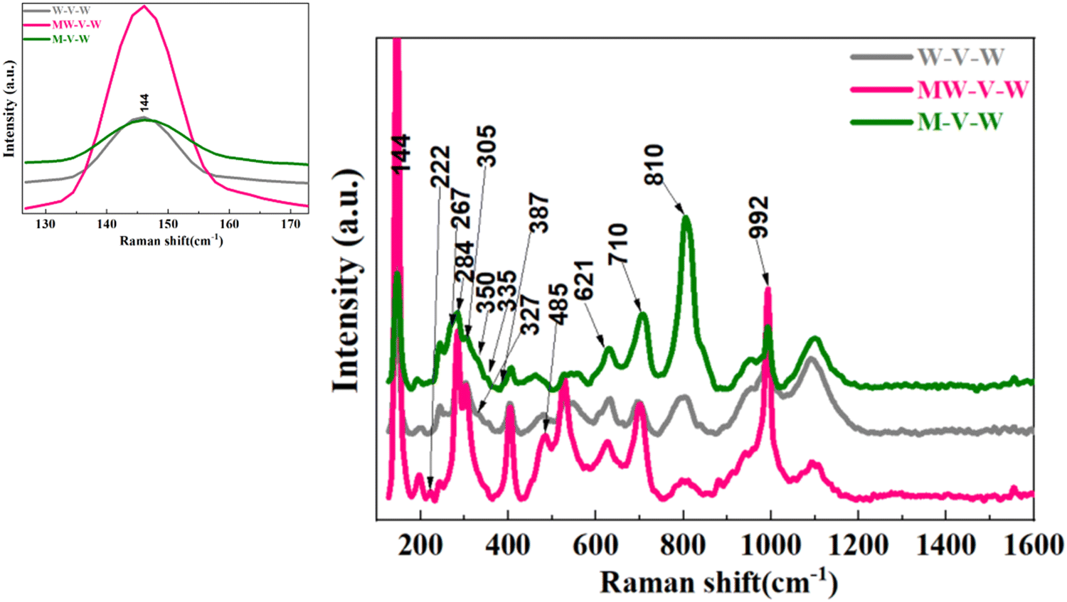 | ||
| Fig. 1 Raman spectra of W–V–W, MoW–V–W, and Mo–V–W samples. The inset shows the main VO2 peak at 144 cm−1. | ||
2. Surface morphology of the top window-layer
It is known that VO2 is one of the attractive, strongly correlated oxides that involve high lattice strain effects that can easily control the deposition of various materials on its surface. Different studies show that reactive DC magnetron sputtering is used to deposit nanowires and nanorods with a high aspect ratio.44 The growth of different morphologies of VO2 has been controlled in the sputtering system, as reported before.45 Our previous research28 delved into the growth patterns of various metal oxides at 400 °C. Fig. S1(a) and (b) (ESI†) in the additional information section show the surface structures of VO2 and MoO3 thin films. By employing high vacuum conditions during deposition, coupled with an optimal sputtering temperature of 40 °C, we achieved the ideal setting for generating nanostructures and uniformly distributed thin films. Notably, nanowires manifest in VO2, while MoO3 exhibits growth in the form of nanosheets. However, depositing the sandwich structure affects the surface growth of the VO2 layer due to its lattice strain, which can influence the growth of MoO3 on its surface.The top FE-SEM images of W–V–W, MoW–V–W, and Mo–V–W sandwich samples unveil a fascinating evolution of nanowire-based structures, shedding light on the intricate nature of these composite materials. In Fig. 2(a) and (b), the W–V–W sample exhibits an initial morphology characterized by a dense and compact structure, with large grains (approximately 139 nm in size) uniformly distributed. However, in Fig. 2(c) and (d), with an increased concentration of Mo in the top layer of the MoW–V–W sample, the presence of delicate nanowires becomes evident, signifying the early stages of surface morphology transformation. Observations indicate the presence of nanostructured wires, with dimensions of roughly 60 nm in length and 20 nm in diameter, which appear to develop atop the grains. This formation results in clearly demarcated regions separated by grain boundaries.
 | ||
| Fig. 2 FE-SEM images of (a) and (b) W–V–W, (c) and (d) MoW–V–W, and (e) and (f) Mo–V–W samples. (a), (c), and (e) show a high resolution of 250 KX, while (b), (d), and (f) represent 50 KX resolutions. | ||
As the process continues, further increasing the Mo atom concentration until reaching MoO3 on the top surface, a profound transformation is observed, resulting in a well-defined and visible nanostructured surface. Fig. 2(e) and (f) depicts the Mo–V–W sample, where short nanowires are uniformly distributed across the entire surface. Notably, the nanoparticles' size remains unchanged compared to the MoW–V–W sample. These short nanowires, characterized by their slender and tapered structures, significantly contribute to the overall surface texture, providing a light-harvesting surface that holds great promise for applications in intelligent windows.
3. XPS
To seek the origin of different thermochromic properties of samples upon varying the top layer of the sandwich structure, the XPS analysis is carried out on both the Mo–V–W and W–V–W samples to examine the composition and valence states of the prepared films. The corresponding results are displayed in Fig. 3 and 4. In Fig. 3(a), the analysis of Mo–V–W and the XPS spectra revealed the presence of the V2p, O1s (Fig. 3(b)), and Mo3d (Fig. 3(c)) photoelectron spectra. The peaks were deconvoluted using a Gaussian function to ascertain the films' chemical state and stoichiometry. Due to spin–orbit splitting, the V2p3/2 spectra display characteristic two-peak patterns at 517.1 eV and 517.9 eV, corresponding to the oxidation states of V4+ and V5+, respectively. For O1s, the core peak was split into two peaks corresponding to an oxygen ion “O2−” at 530 eV and oxygen vacancies “VO2+” at 533.12 eV. High-resolution XPS in Fig. 3(c) showed the enlarged spectra of Mo3d between 227 eV and 240 eV binding energies, which exhibited dual peaks, with Mo3d5/2 and Mo3d3/2 peaks. These peaks correspond to molybdenum in Mo6+ oxidation states. The binding energy difference of Mo3d5/2 and Mo3d3/2 is 3.12 eV, which fits well with the reported values.46,47 | ||
| Fig. 3 (a) XPS survey spectrum of the M–V–W sample. (b) Enlarged spectra of V 2p3/2, V 2p1/2, and O 1s and (c) Mo 3d peaks. | ||
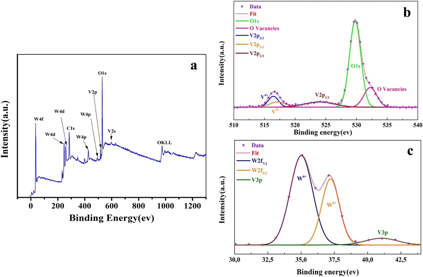 | ||
| Fig. 4 (a) XPS survey spectrum of the W–V–W sample. (b) Enlarged spectra of V 2p3/2, V 2p1/2, and O 1s and (c) W 2f and V 3p peaks. | ||
The XPS analysis of the W–V–W sample is presented in Fig. 4. The survey spectrum in Fig. 4(a) shows the existence of O, W, and V. Deconvolution of V2p3/2 also reveals two peaks at 516.41 eV and 517.11 eV, for V4+ and V5+, oxidation states, respectively. The high resolution of the O1s core peak shows an oxygen ion peak of “O2−” at 529.78 eV and oxygen vacancies “VO2+” at 532.24 eV (Fig. 4(b)).48 In addition, from the deconvolution of the W4f core peak in Fig. 4(c), W is present as W6+ with W4f7/2 and W2f5/2 at 35.02 eV and 37.21 eV binding energies, respectively. These binding energies were consistent with previously published values of the W6+ oxidation state WO3.38,42
The integrated surface ratio of V4+/V5+ in Mo–V–W is 1.87, indicating a higher proportion of V4+ valence than the W–V–W sample, which presents a lower V4+/V5+ ratio of 1.37. It is generally thought that W6+ and Mo6+ as solutes penetrate the crystal lattice of VO2 and substitute the V4+ ion, creating donor-like defects (both W6+ and Mo6+ ions with valences higher than V4+ ions). The lower V4+/V5+ ratio in the W–V–W sample relative to the Mo–V–W sample is attributed to the possibility of over-doping VO2 thin films by W atoms migrating from both upper and lower layers.47 However, in the Mo–V–W sample, the co-doping of W6+ and Mo6+ ions contribute separately to the increasing V4+/V5+ ratio.19,49,50
4. Electrical properties
Fig. 5 illustrates the temperature-dependent sheet resistivity of V, W–V–W, MoW–V–W, and Mo–V–W samples. The graph showcases the variation in sheet resistivity with changing temperatures. Initially, all samples exhibit thermochromic properties with a relatively high sheet resistivity in KΩ order (Table 2). As the temperature increases, a significant decrease in sheet resistivity of up to four orders of magnitude is observed for the samples with MoO3 as a window layer. This remarkable change indicates a notable improvement in the electrical conductivity properties of the sandwich samples compared to the reference sample V. | ||
| Fig. 5 Temperature-dependent sheet resistivity of (a) V, (b) W–V–W, (c) MoW–V–W, and (d) Mo–V–W samples. Tc calculated from d(logR)/dT ∼ T with Gauss fitting plots in insets. | ||
| Samples | T c (°C) | ΔR (Ω cm−1) | ΔH (°C) |
|---|---|---|---|
| V | 54 | 1.7 × 10² | 12 |
| W–V–W | 43 | 1.95 × 10² | 9.6 |
| MoW–V–W | 43.6 | 3.5 × 10² | 6 |
| Mo–V–W | 36.8 | 3.78 × 10² | 14.8 |
The amplitude of transition (ΔR), representing the resistance change from room temperature above 85 °C, and the hysteresis widths (ΔH), calculated as the difference between Tc values measured during heating and cooling cycles are also discussed. The Tc value of the W–V–W sample with a WO3 window layer is 43 °C, while for the MoW–V–W sample with a Mo0.2W0.8O3 window layer, it is 43.6 °C. However, Mo–V–W samples presented the lowest recorded Tc behavior of 36.8 °C. Those values of the three samples are lower than the observed transition temperature of VO2 of the order 54 °C.
Furthermore, the ΔR and ΔH values change according to the window layer used in W–V–W, MoW–V–W, and Mo–V–W samples. Comparatively, the W–V–W sample deposited with a WO3 window layer exhibits a lower ΔR value of 1.95 × 10² Ω cm−2, while MoW–V–W with the Mo0.2W0.8O3 window layer presented a narrower ΔH of 6 °C with a high ΔR of 3.5 × 10² Ω cm−2, indicating superior electrical behavior compared to the V sample with the smallest ΔR (1.7 × 10² Ω cm−2) and a ΔH value of 12 °C. Mo–V–W presented a higher ΔR of 3.78 × 10² Ω cm−2 and the lowest Tc of 36.8 °C. However, this sample presents the highest hysteresis ΔH of 14.8 °C.
A longstanding debate surrounds the nature of the metal–insulator transition (MIT) in VO2. Some argue for a Mott-type transition, emphasizing strong electron–electron correlations, while others advocate for a Peierls-type transition, focusing on structural changes involving V dimerization. Recently, a hybrid perspective has emerged, proposing that the MIT in VO2 might be best described as a Mott-Peierls phase transition, suggesting that electron–electron correlations and V4+ dimerization contribute significantly to this transition.51–53 As evidenced by the XPS findings, the W–V–W configuration exhibits a lower V4+/V5+ ratio compared to the Mo–V–W configuration. Consequently, the Tc of the Mo–V–W samples is lower than that of the W–V–W samples. Despite the low Tc of Mo–V–W, the Mo migration to the VO2 lattice results in a broadening of the phase transition peak (bigger ΔH); this effect is likely due to the substitution of V in the VO2 lattice by Mo through doping. Mo will replace the position of V in the doping process because the radius of Mo6+ is more significant than that of V4+, which results in the deformation of its crystalline structure due to the size mismatch. This disparity in ionic radii between Mo6+ and V4+ leads to decreased activation energy required for MIT, resulting in a bigger ΔH and a phase transition sharpness.49,54–56 The work done by Fan et al.57 indicated that the high defect concentration would cause a hysteresis loop or disappearance of the shifting effect.
5. Optical properties
The optical transmittance of samples was measured in visible (vis) and near-infrared (NIR) regions under two different temperatures (room temperature (RT); 25 °C and 80 °C) of the V, W–V–W, MoW–V–W, and Mo–V–W samples. It is evident from the presented results in Fig. 6 that the transmittance in the visible region remains relatively constant for all the samples. The following formulas were used to calculate the integrated solar transmittance (Tsol, 300–2500 nm) and luminous transmittance (Tlum, 380–780 nm)58:In this case, φlum(λ) is the standard luminous efficiency function for the human photopic vision, T(λ) indicates the film transmittance at a wavelength (λ), and φsol(λ) is the solar irradiance spectrum for air mass 1.5, which corresponds to the sun standing 37° above the horizon and ΔTsol is the solar modulation ability.

 | ||
| Fig. 6 Transmittance spectra at RT and 80 °C of (a) V, (b) W–V–W, (c) MoW–V–W, and (d) Mo–V–W samples. | ||
To use VO2 in smart windows applications, a technological obstacle is to raise the maximum Tlum to a respectable level (>50%) while preserving VO2's high ΔTsol.59 The solar transmittance of each sample was computed as a means of illustrating the solar modulation. The calculated Tsol on the solar spectra present a similar comportment as Tlum. This suggests that the structures under investigation have a large impact on the transmission of not only in the visible light range but also in the entire solar spectra.
As presented in Fig. 7, Tlum calculated from the transmittance spectra at the RT, it presents a slight decrease from 45.33% to 41.65% in the W–V–W sample compared to the VO2 thin films’ reference sample (Table 3). The sandwich structure negatively affected the sample's transmittance in W–V–W due to the additional two WO3 layers.48 On the other hand, ΔTsol increased to from 9.57% in VO2 to 15.7%. Nevertheless, a considerable improvement in both MoW–V–W and Mo–V–W of 50.83% and 54.57% was noticed. In contrary to the W–V–W surface, the nanostructured surface of MoW–V–W and Mo–V–W acted as a light-harvesting media reducing the reflectance arrived from the VO2 surface and acting as an antireflecting layer. Consequently, we notice a very promising improvement in Tlum. Additionally, in Table 3, Tlum improvement can be seen to have a direct relationship with the sandwich samples' optical band gap (Eg).7,54 ΔTsol decreases in Mo–V–W and MoW–V–W to 12.43% and 9.25%, respectively, compared to the W–V–W sample. It is believed that the defects generated due to the textured surface negatively affected the solar modulation of these two samples.
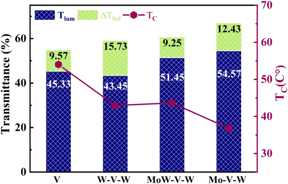 | ||
| Fig. 7 Bar plots of Tlum, ΔTsol and Tc of V, W–V–W, MoW–V–W and Mo–V–W samples. | ||
| Samples | T lum | T sol | ΔTsol | T c (°C) |
|---|---|---|---|---|
| V | 45.33 | 46.86 | 9.57 | 54 |
| W–V–W | 41.65 | 43.45 | 15.73 | 43 |
| MoW–V–W | 50.83 | 51.45 | 9.25 | 43.6 |
| Mo–V–W | 54.57 | 52.49 | 12.43 | 36.8 |
IV. Conclusions
In conclusion, the systematic investigation of nanowire-based sandwich-structured thin films composed of Mo0.2W0.8O3, MoO3, and WO3 top layers via physical vapor deposition provides a detailed understanding of their structural, electrical, and optical characteristics. Raman spectroscopy confirms the successful preparation of each thin film, highlighting distinctive vibrational modes and lattice features. FE-SEM images reveal a fascinating evolution of nanostructures, particularly with MoO3 as the top layer, showcasing potential applications in smart window applications. Electrical properties exhibit significant improvements in conductivity for samples with MoO3 as a window layer, attributing this enhancement to the migration of Mo atoms into the VO2 lattice. The observed MIT behavior is rationalized based on XPS findings. Furthermore, optical analysis demonstrates promising improvements in luminous transmittance and solar modulation, especially in configurations with MoO3 as the top layer. Collectively, these findings contribute to the knowledge base for developing and optimizing multifunctional thin films, paving the way for potential advancements in smart window technologies.Data availability
Will be available on request.Conflicts of interest
The authors declare that they have no known competing financial interests or personal relationships that could have appeared to influence the work reported in this paper.Acknowledgements
The authors acknowledge the support from the Scientific Research Projects Coordination (BAP) – Konya Necmettin Erbakan University (NEÜ), under Project Number: 191319007 for Yasin Ramazan Eker and Mohamed A. Basyooni. The authors also acknowledge the support from the Science and Technology Research and Application Center (BITAM), Konya Necmettin Erbakan University (NEÜ).References
- P. Huovila, et al., Buildings and climate change: Summary for decision-makers, 2009 Search PubMed.
- L. Pérez-Lombard, J. Ortiz and C. Pout, A review on buildings energy consumption information, Energy Build., 2008, 40(3), 394–398 CrossRef.
- Z. Zhang, et al., Thermochromic Energy Efficient Windows: Fundamentals, Recent Advances, and Perspectives, Chem. Rev., 2023, 123(11), 7025–7080 CrossRef.
- K. Okimura, et al., High luminous transmittance and solar modulation of VO2-based smart windows with SiO2 anti-reflection coatings, Sol. Energy Mater. Sol. Cells, 2023, 251, 112162 CrossRef.
- M. K. Shahzad, et al., Influence of VO2 based structures and smart coatings on weather resistance for boosting the thermochromic properties of smart window applications, RSC Adv., 2022, 12(48), 30985–31003 RSC.
- J. Victor, et al., From multilayers to V1−xWxO2 ± δ films elaborated by magnetron sputtering for decreasing thermochromic transition temperature, J. Alloys Compd., 2021, 858, 157658 CrossRef.
- D. Zhou, et al., Symmetrical SnO2/W-doped VO2/SnO2 sandwich structures with high luminous transmittance, excellent solar modulation ability and low phase transition temperature, Infrared Phys. Technol., 2022, 123, 104198 CrossRef.
- H. Zhou, et al., Surface plasmon resonance tunability in VO2/Au/VO2 thermochromic structure, Laser Photonics Rev., 2014, 8(4), 617–625 CrossRef.
- Y. Dang, L. Zhao and J. Liu, Preparation and optical properties of W-doped VO2/AZO bilayer composite film, Ceram. Int., 2020, 46(7), 9079–9085 CrossRef.
- H. Zong, et al., Preparation and characterization of HfO2/VO2/HfO2 sandwich structures with low phase transition temperature, excellent thermochromic properties, and superior durability, Ceram. Int., 2022, 48(5), 6734–6744 CrossRef.
- D. Malarde, et al., Optimized atmospheric-pressure chemical vapor deposition thermochromic VO2 thin films for intelligent window applications, ACS Omega, 2017, 2(3), 1040–1046 CrossRef PubMed.
- H. Koo, et al., The effect of CeO2 antireflection layer on the optical properties of thermochromic VO2 film for smart window system, J. Mater. Eng. Perform., 2014, 23, 402–407 CrossRef.
- H.-T. Zhang, et al., Wafer-scale growth of VO2 thin films using a combinatorial approach, Nat. Commun., 2015, 6(1), 8475 CrossRef PubMed.
- J. Kim, et al., Two-dimensional VO2 nanosheet converted from MXene for flexible thermochromic smart windows, Chem. Eng. J., 2023, 477, 147014 CrossRef.
- H. Koo, et al., Thermochromic properties of VO2 thin film on SiNx buffered glass substrate, Appl. Surf. Sci., 2013, 277, 237–241 CrossRef CAS.
- G. Xu, et al., Optimization of antireflection coating for VO2-based energy efficient window, Sol. Energy Mater. Sol. Cells, 2004, 83(1), 29–37 CrossRef CAS.
- H. Kim, et al., Strain effect in epitaxial VO2 thin films grown on sapphire substrates using SnO2 buffer layers, AIP Adv., 2017, 7(10), 105116 CrossRef.
- J. Zheng, S. Bao and P. Jin, TiO2 (R)/VO2 (M)/TiO2 (A) multilayer film as smart window: Combination of energy-saving, antifogging and self-cleaning functions, Nano Energy, 2015, 11, 136–145 CrossRef.
- S. Long, et al., Thermochromic multilayer films of WO3/VO2/WO3 sandwich structure with enhanced luminous transmittance and durability, RSC Adv., 2016, 6(108), 106435–106442 RSC.
- S.-Z. Sheng, et al., Nanowire-based smart windows combining electro-and thermochromics for dynamic regulation of solar radiation, Nat. Commun., 2023, 14(1), 3231 CrossRef PubMed.
- L. Veeramuthu, et al., Novel stretchable thermochromic transparent heaters designed for smart window defroster applications by spray coating silver nanowire, RSC Adv., 2019, 9(61), 35786–35796 RSC.
- L. L. Zhao, et al., Enhanced Thermochromic Properties and Solar-Heat Shielding Ability of Wx V1–x O2 Thin Films with Ag Nanowires Capping Layers, J. Nanosci. Nanotechnol., 2015, 15(11), 9192–9196 CrossRef.
- D. Y. Lu, et al., Raman study of thermochromic phase transition in tungsten trioxide nanowires, Appl. Phys. Lett., 2007, 90(4), 041919 CrossRef.
- W. Y. Wu, et al., Thermochromism from Ultrathin Colloidal Sb2Se3 Nanowires Undergoing Reversible Growth and Dissolution in an Amine–Thiol Mixture, Adv. Mater., 2019, 31(4), 1806164 CrossRef.
- K. C. Kam and A. K. Cheetham, Thermochromic VO2 nanorods and other vanadium oxides nanostructures, Mater. Res. Bull., 2006, 41(5), 1015–1021 CrossRef.
- M. A. Basyooni, et al., Efficient MoWO3/VO2/MoS2/Si UV Schottky photodetectors; MoS2 optimization and monoclinic VO2 surface modifications, Sci. Rep., 2020, 10(1), 1–18 CrossRef.
- K. Appavoo, et al., Role of defects in the phase transition of VO2 nanoparticles probed by plasmon resonance spectroscopy, Nano Lett., 2012, 12(2), 780–786 CrossRef.
- M. A. Basyooni, et al., Fast response of CO2 room temperature gas sensor based on Mixed-Valence Phases in Molybdenum and Tungsten Oxide nanostructured thin films, Ceram. Int., 2020, 46(7), 9839–9853 CrossRef.
- M. Currie, M. A. Mastro and V. D. Wheeler, Atomic layer deposition of vanadium dioxide and a temperature-dependent optical model, J. Visualized Exp., 2018,(135), e57103 Search PubMed.
- A. Makarevich, et al., Chemical synthesis of high quality epitaxial vanadium dioxide films with sharp electrical and optical switch properties, J. Mater. Chem. C, 2015, 3(35), 9197–9205 RSC.
- X.-B. Chen, Assignment of the Raman modes of VO2 in the monoclinic insulating phase, J. Korean Phys. Soc., 2011, 58, 100–104 CrossRef CAS.
- T. Nagyné-Kovács, et al., Hydrothermal synthesis and gas sensing of monoclinic MoO3 nanosheets, Nanomaterials, 2020, 10(5), 891 CrossRef PubMed.
- P. Martín-Ramos, et al., α-MoO3 crystals with a multilayer stack structure obtained by annealing from a lamellar MoS2/g-C3N4 nanohybrid, Nanomaterials, 2018, 8(7), 559 CrossRef.
- T. Ivanova, K. Gesheva and A. Szekeres, Structure and optical properties of CVD molybdenum oxide films for electrochromic application, J. Solid State Electrochem., 2002, 7, 21–24 CrossRef CAS.
- C. W. Kee, Assignment of O–O and Mo = O stretching frequencies of molybdenum/tungsten complexes revisited, J. Chem., 2015, 2015, 10 Search PubMed.
- A. Klinbumrung, T. Thongtem and S. Thongtem, Characterization of orthorhombic α-MoO3 microplates produced by a microwave plasma process, J. Nanomater., 2012, 2012, 10 Search PubMed.
- F. Haque, et al., Ordered intracrystalline pores in planar molybdenum oxide for enhanced alkaline hydrogen evolution, J. Mater. Chem. A, 2019, 7(1), 257–268 RSC.
- F. Liu, et al., Ultrathin tungsten oxide nanowires: oleylamine assisted nonhydrolytic growth, oxygen vacancies and good photocatalytic properties, RSC Adv., 2015, 5(94), 77423–77428 RSC.
- J. Díaz-Reyes, et al., Characterization of WO3 thin films grown on silicon by HFMOD, Adv. Condens. Matter Phys., 2013, 2013, 9 CrossRef.
- H. Choi, et al., Mid-infrared properties of a VO2 film near the metal-insulator transition, Phys. Rev. B: Condens. Matter Mater. Phys., 1996, 54(7), 4621 CrossRef.
- M. A. B. Mohamed, VO2 İnce Film İçeren İki Boyutlu ve Çok Katmanlı Yapılardaki Arayüzey Gerilmelerinin Termokromik ve Fotodetektör Performanslara Etkisi, Necmettin Erbakan University, Turkey, 2020 Search PubMed.
- J. Díaz-Reyes, et al., Characterization of WO3 thin films grown on silicon by HFMOD, Adv. Condens. Matter Phys., 2013, 2013, 9 Search PubMed.
- M. A. Basyooni, et al., Tuning the metal–insulator transition properties of VO2 thin films with the synergetic combination of oxygen vacancies, strain engineering, and tungsten doping, Nanomaterials, 2022, 12(9), 1470 CrossRef CAS PubMed.
- S.-Y. Li, et al., Thermochromic VO2 nanorods made by sputter deposition: Growth conditions and optical modeling, J. Appl. Phys., 2013, 114(3), 033516 CrossRef.
- T. D. Vu, HiPIMS deposition of VO2 thermochromic coating for enhanced optical properties, 2022 Search PubMed.
- Z. Li, L. Gao and S. Zheng, SEM, XPS, and FTIR studies of MoO3 dispersion on mesoporous silicate MCM-41 by calcination, Mater. Lett., 2003, 57(29), 4605–4610 CrossRef.
- V. Sreelakshmi, A. A. Kaliani and M. Jithin, Photochromic and hydrophilic vanadium oxide–molybdenum oxide composite thin films, J. Mater. Sci.: Mater. Electron., 2023, 34(3), 179 CrossRef.
- Z. Fang, et al., VO2/ZnO bilayer films with enhanced thermochromic property and durability for smart windows, Appl. Surf. Sci., 2021, 540, 148414 CrossRef.
- F. Chen, et al., Simultaneous tuning of the phase transition temperature and infrared optical properties of Mo-doped VO2 powders for intelligent infrared stealth materials, Ceram. Int., 2023, 49(15), 25585–25593 CrossRef.
- D. Li, et al., Influence of the charge compensation effect on the metal–insulator transition of Mg-W co-doped VO2, Appl. Surf. Sci., 2022, 579, 151990 CrossRef.
- N. F. Mott, The basis of the electron theory of metals, with special reference to the transition metals, Proc. Phys. Soc., Sect. A, 1949, 62(7), 416 CrossRef.
- C. Ling, et al., W Doping and Voltage Driven Metal-Insulator Transition in VO Nano -Films for Smart Switching Devices, ACS Appl. Nano Mater., 2019, 2(10), 6738–6746 CrossRef.
- S. Biermann, et al., Dynamical singlets and correlation-assisted peierls transition in VO2, Phys. Rev. Lett., 2005, 94(2), 026404 CrossRef.
- C. Kang, et al., Transformation of crystalline structure and photoelectric properties in VO2/glass thin films by inserting TiO2 buffer layers, Appl. Surf. Sci., 2019, 463, 704–712 CrossRef.
- C. W. Jo, H. J. Kim and J. W. Yoo, Thermochromic Properties of W-Mo Co-Doped VO(M) Nanoparticles According to Reaction Parameters, J. Nanosci. Nanotechnol., 2017, 17(5), 2923–2928 CrossRef.
- Y. Xue and S. Yin, Element doping: a marvelous strategy for pioneering the smart applications of VO2, Nanoscale, 2022, 14(31), 11054–11097 RSC.
- L. Fan, et al., Modulation of VO2 metal-insulator transition by co-doping of hydrogen and oxygen vacancy, Sol. Energy Mater. Sol. Cells, 2020, 212, 110562 CrossRef.
- M. A. Abozeid, et al., Development of nano-WO3 doped with NiO for wireless gas sensors, Arabian J. Sci. Eng., 2019, 44(1), 647–654 CrossRef.
- M. Zhou, et al., Periodic porous thermochromic VO2 (M) films with enhanced visible transmittance, Chem. Commun., 2013, 49(54), 6021–6023 RSC.
Footnote |
| † Electronic supplementary information (ESI) available. See DOI: https://doi.org/10.1039/d3cp05942a |
| This journal is © the Owner Societies 2024 |