The role of pressure on lattice thermal conductivity and its related thermodynamical parameters in In0.53Ga0.47As nanofilms
Received
24th November 2023
, Accepted 22nd December 2023
First published on 4th January 2024
Abstract
Lattice thermal conductivity (LTC) for In0.53Ga0.47As alloy films, with thicknesses ranging from 10 nm to 1.4 μm, was investigated under pressures of up to 11 GPa and temperatures between 1 and 450 K, utilizing the modified Debye–Callaway model. The effects of structural and thermodynamical parameters, as well as phonon interactions, on LTC were examined. The Clapeyron, Murnaghan, and Post equations were applied to determine the pressure dependence of the melting temperature, lattice volume, and Debye temperature, respectively. A novel derivative form of the bulk modulus, suitable for nanomaterials, has been introduced. It was found that decreasing the film thickness increases the Gruneisen parameter, while increasing pressure decreases it. The LTC of nanofilms is significantly affected by their thickness and pressure strength; notably, under 11 GPa, films with a thickness of 10 nm exhibit a substantial decrease in LTC. LTCmax declines due to the greater influence of boundary scattering compared to dislocations. These findings suggest potential applications in managing nanofilm temperature and size, which are key to advancing nanomaterials and enhancing the efficiency of electronic devices.
1. Introduction
In recent decades, researchers have focused on the thermal conductivity of nanostructured materials1,2 due to its direct relation to the efficiency of thermal dissipation. Accurate calculation of lattice thermal conductivity is crucial for designing high-quality nano-electronic3 power devices,4,5 generating transistors,6 and thermoelectric generators. Hydrostatic pressure serves as a principal thermodynamic variable used to accelerate reactions, design novel structures, and define the properties of nanostructures.7,8 Pressure is a significant factor in semiconductor behavior, meriting further study.9 The alloy In0.53Ga0.47As, formed from InAs and GaAs, has a zinc blende structure with a lattice parameter a(∞) of 5.868 Å10 and a direct band gap, making it suitable for high-performance photodiodes.11 Its nanofilms are versatile, and used in devices for their radiation resistance and durability.12 The alloy's applications now include lasers,13 photodetectors,14 transistors,5,15 and photovoltaics,5,15 with transistors being prevalent in modern electronics like smartphones and computers.
Pressure's impact on thermal conductivity16 is key for understanding phase transitions and material properties, and is studied both theoretically and experimentally. The process is vital in fields such as astrophysics and geosciences. Many authors have predicted theoretical calculations of the pressure effect on size-dependent LTC in InAs nanowires, Si nanofilms, and multilayer hexagonal boron nitride.17–19 Theoretical models predict how pressure affects the lattice thermal conductivity (LTC) in various nanostructures, aiding in the design and analysis of their physical and thermal properties.7 For In0.53Ga0.47As nanofilms, such analysis is crucial as it allows for precise LTC calculations under pressure. However, for validating these results, experimental data exist only for the zero pressure LTC of In0.53Ga0.47As films (10 nm–1.4 μm),5,20 making these findings useful for overcoming experimental challenges in other pressure ranges of up to 11 GPa, where the challenges could range from technical and financial constraints. The Clapeyron model, utilized in this work, is preferred due to its broad application in analyzing phase transitions, such as melting, because it describes how pressure affects the melting temperature. It is now also applicable at the nanoscale.17–19 In contrast, other used models, e.g. the DNA melting model, are specifically designed for DNA's thermal denaturation, considering nucleotide sequences and hydrogen bonds. The Clapeyron model predicts shifts in melting temperature with changes in pressure along phase boundaries, while the DNA model's temperature is determined by the genetic composition and stability of the DNA strands.21–24
In this work, the size-dependent LTC for In0.53Ga0.47As nanofilms will be determined by using the modified Debye–Callaway model with the effects of hydrostatic pressure depending on the Murnaghan lattice parameter.25 The Clapeyron equation for melting temperature Tm,23,24 the Gruneisen parameter γ, which is derived from the Rice equation of measuring shock-waves,26,27 the average phonon group velocity vave,28 Debye temperature θD,29 surface energy σsl24 and surface stress fsl,30 and the bulk modulus B31 with its first derivative B′ representing new values appropriate for In0.53Ga0.47As nanofilms, have been determined through a fresh derivation of the nanomaterial form. This approach was initially utilized by Hofmeister in 2002 for bulk materials.32 On the assumption that the dimensions at the nanoscale do not have an impact on impurities and electronic behavior, a size-dependent density ρ31 is calculated for all the film's thicknesses. This work examines how the lattice thermal conductivity (LTC) of nanofilms is influenced by their thickness and the amount of pressure they can withstand. In practical terms, these insights could lead to more efficient thermal management in electronic devices, as In0.53Ga0.47As is known for its semiconductor properties. The potential implications include improved performance and reliability in high-tech applications, such as faster processors33 and advanced sensors.33
2. Methods of calculation
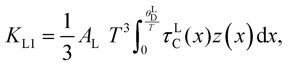
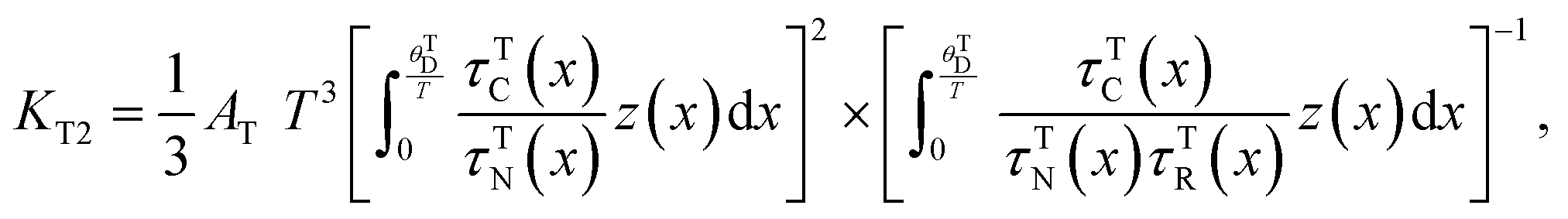
The Debye–Callaway model that is modified by Asen-Palmer et al.34 and Morelli et al.35 is used to determine the LTC in In0.53Ga0.47As bulk (thick) and nanofilms. The model includes both modes of one longitudinal KL and two degenerate transverse (KT) phonon branches, whilst acoustic phonon branches mostly contribute to heat conduction in semiconductors.36,37 The temperature dependence of LTC in solids can be expressed as:35where transverse and longitudinal branches are denoted by T and L, respectively. The partial conductivity term of the modified Debye–Callaway model can be given by KL1 and KL2, as in the following form:35| |  | (4) |
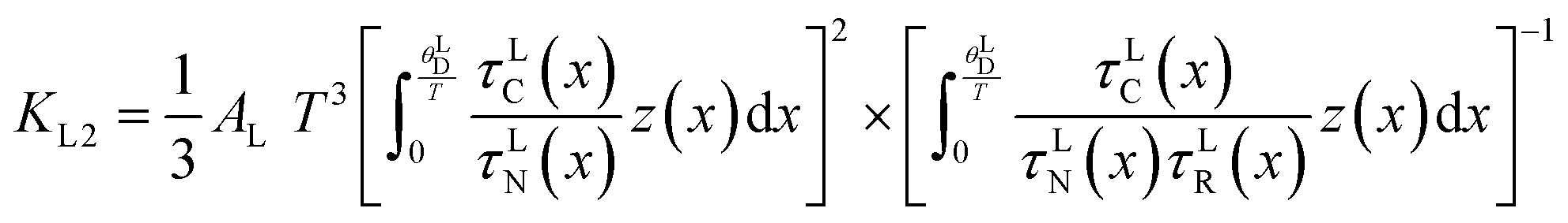
| |  | (5) |
The transverse contribution has two forms, which are as follows:| |  | (6) |
| |  | (7) |
| |  | (8) |
where z(x) = x4ex(ex − 1)−2,  , ħ, kB, T, v and ω are the Planck constant (1.05457 × 10⁻³⁴ J s), Boltzmann's constant (1.38065 × 10⁻²³ m2 kg s−2 K−1), absolute temperature, acoustic phonon group velocity and phonon frequency, respectively. The combined phonon-scattering is denoted by τC(x),38 while τR(x) is the resistive total scattering. Furthermore, both branches of Debye temperature are determined by θL(T)D:35
| |  | (9) |
while the dispersion of phonon branches near the zone boundary is ignored. The resistive scattering processes (τL(T)R)−1 are estimated by:20| | | (τL(T)R)−1 = (τL(T)U)−1 + (τL(T)M)−1 + (τL(T)b)−1 + (τL(T)ph–e)−1 + (τL(T)DC)−1, | (10) |
where τU, τM, τb, τph–e, and τDC are the umklapp, impurity, boundary, phonon–electron, and dislocation scattering, respectively. Accordingly, the combined phonon scattering process (τL(T)C)−1 is as follows:| | | (τL(T)C)−1 = (τL(T)N)−1 + (τL(T)R)−1. | (11) |
The detailed phonon scattering processes are as follows:
2.1 Umklapp scattering
This mechanism involves phonons colliding and transferring momentum to the crystal lattice, resulting in thermal resistance. It becomes more prominent at elevated temperatures and higher phonon frequencies, which is given by:35,39| |  | (12) |
where (γL(T)) represents the longitudinal (transverse) Gruneisen parameters, and their values are given by γL(∞) = 0.3 and γT(∞) = 0.22. These values were determined by fitting theoretical LTC to the experimental data from the bulk state of In0.53Ga0.47As.
2.2 Normal scattering
Normal phonon scattering involves phonons being deflected by interactions that preserve their wave vector and net momentum. This scattering type is often overlooked compared to umklapp processes, and is computed based on:35,39| | 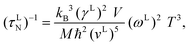 | (13) |
| |  | (14) |
2.3 Boundary scattering
The surfaces and interfaces of nanofilms play a crucial role in phonon scattering. Phonons can be reflected or absorbed at these boundaries, according to:| |  | (15) |
2.4 Defect scattering
The presence of defects in the lattice can scatter phonons, affecting LTC. The strength of this scattering is contingent upon the material's dispersion curves. The Rayleigh scattering theorem elucidates the interactions between high-frequency phonons and three distinct defect types: impurities (foreign atoms), isotopes, and alloy disorder parameters:40,41| | 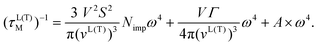 | (16) |
(Nimp) represents the concentration of impurities, while (S) denotes the scattering factor, typically around the value of 1. The term for alloy scattering defined at which phonons scatter with the alloy is comparable to the rate of phonon-isotope scattering. The parameter (A) signifies the alloy parameter, which quantifies the intensity of the alloy's scattering effect,42 and is calculated by  , representing the strength of the mass difference interaction, which for In0.53Ga0.47As, is calculated as follows:43
| |  | (17) |
2.5 Phonon–electron scattering
In semiconductors and other materials with free electrons, interactions between phonons and electrons can scatter phonons, influencing LTC. Zou and Balandin suggested a method for calculating the rate at which phonons scatter with electrons:44| |  | (18) |
Ne represents the density of electrons in the conduction band, E denotes the deformation potential with an approximate value of −7.79 eV,45m* symbolizes the effective mass of an electron, which is (0.041 × me)46 for In0.53Ga0.47As, where me is the resting mass of an electron, and ρ stands for the mass density.
2.6 Dislocation scattering
The rate at which phonons scatter off dislocations, considering a dimensionless parameter for short-range interactions, is determined based on ref. 40 and 41:| |  | (19) |
In this context, η represents the weight factor, which is assigned a value of 0.55, and ND denotes the total concentration of dislocations, encompassing both edge and screw types. Factors influencing phonon scattering: several factors can significantly affect phonon scattering processes in nanofilms:47 in nanofilms, the aforementioned scattering processes can lead to a reduction in LTC compared to bulk materials. This is attributed to the increased surface-to-volume ratio, which amplifies the impact of surface scattering mechanisms. Additionally, confinement effects can alter the phonon spectrum, leading to changes in LTC. An understanding of these processes and their dependencies is crucial for the design of materials with tailored thermal properties.
2.7 Nanofilm dependencies: pressure and size factors
The aforementioned principle can be used when there is no pressure. Considering pressure, which is an important parameter and affects most properties of solids, the model can be applied to the effect of pressure on LTC in In0.53Ga0.47As thick and nanofilms of up to 11 GPa, with modifications of other thermophysical properties, including melting temperature. The bulk solid's melting temperature, Tm(r,P), dependent on pressure, is calculated using the Clapeyron equation:23,24,48| |  | (20) |
The Clapeyron equation, in its simplified form (first-order approximation) as a function of size and pressure, allows for easier calculations and can still provide a general understanding of phase behavior, which is useful for nanofilms, calculating the melting temperature.23,24Tm0, using variables: molar volume Vs and Vl, for solid and liquid states, respectively. Here, Vs is the product of the zero-pressure lattice volume V and Avogadro's number NA,23 while Vl is 90% of Vs. Compressibility Ks, and Kl are defined as (Ks = 1/B), where B is the bulk modulus, and Kl is typically ten times Ks, and Hm is the melting enthalpy. Surface energy σsl and stress fsl are critical thermodynamic parameters (Table 1), particularly for calculating Tm(P).
Table 1 Parameters are obtained through equations stated in the text for both the bulk and nanofilms of In0.53Ga0.47As
| Material parameters |
Thick films 1.4 μm (bulk) |
Nanofilm thickness |
| 70 nm |
30 nm |
20 nm |
10 nm |
|
B (GPa) |
58.0666 |
56.8123 |
55.1463 |
53.6953 |
49.383 |
|
V
s (cm3 mol−1) |
15.215 |
15.3861 |
15.6263 |
15.8417 |
16.5187 |
|
K
s (10−12 Pa−1) |
17.2216 |
17.6018 |
18.1335 |
18.6263 |
20.2499 |
|
B′ |
1.986 |
1.99026 |
1.99606 |
2.00129 |
2.01785 |
|
v
ave (m s−1) |
3237.18 |
3220.51 |
3197.6 |
3176.93 |
3111.11 |
|
γ
ave
|
0.159678 |
0.1617 |
0.1646 |
0.1673 |
0.1755 |
|
K
l (10−12 Pa−1) |
172.216 |
176.018 |
181.335 |
186.263 |
202.499 |
|
ρ (kg m−3) |
5541.07 |
5477.65 |
5393.45 |
5320.11 |
5102.06 |
|
V
l (cm3 mol−1) |
13.693 |
13.8475 |
14.0637 |
14.2576 |
14.8669 |
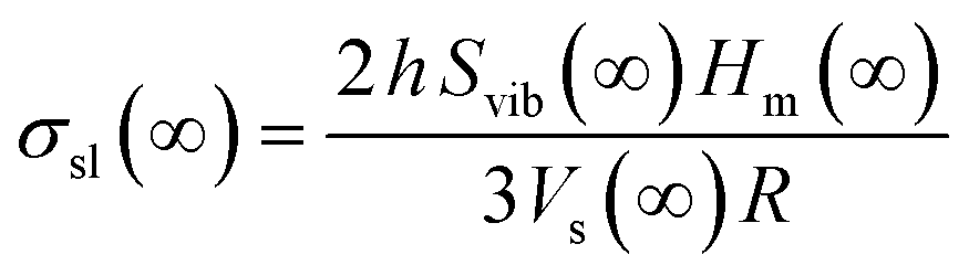
The bulk (thick film in this work) structure surface energy σsl in eqn (20) is calculated according to the Gibbs–Thomson equation:24 , and for nanosized films, it is modified to:
| |  | (21) |
where (∞) and (
r) denote both bulk state (the thick film) and nanofilms,
h is the first solid surface monolayer and calculated from the relation
h = 1.429
dmean(∞),
49 and
Svib is the material's vibrational entropy obtained from
Svib =
Sm −
R.
29dmean(∞) is the mean bond length, and it is dependent on the thickness, where
Sm(∞) and
R are the melting entropy and the gas constant, respectively.
Sm =
Hm/
Tm,
29 where
Hm is the melting enthalpy, and for a tetrahedral compound semiconductor it is calculated from this relation:
50Hm(∞) = −10
−5Tm2(∞) + 0.059
Tm(∞) − 21.33. Its modification for nanosize-dependent solids can be expressed as:
| | | Hm(r) = −10−5Tm2(r) + 0.059Tm(r) − 21.33. | (22) |
The intrinsic surface stress
fsl in
eqn (20) is the pressure effect on the surface creating a lattice contraction and it is a reversible work per unit area, which is calculated according to:
30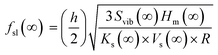
, for nanofilms, the form is modified to:
| |  | (23) |
The bulk modulus
B for the bulk value is calculated from
B(∞) =
vave2(∞)
ρ(∞), and its nanosize-dependent modification is:
31Additionally, the average phonon group velocity for the bulk state is

,
51 and its nanosized modification is as in the following:
| |  | (25) |
where
vL and
vT are the longitudinal and transverse phonon group velocities, respectively. At the nanoscale, the deflection or reflection of phonons depends strongly on the size. The mean bond length
dmean(∞) at high temperature is an average distance for a phonon. Its change according to the nanosize scale Δ
dmean(
r) is given by:
49| |  | (26) |
where
r is half of the nanofilm thickness, and
rc is the critical radius at which the material melts at zero Kelvin and calculated by
rc = (3 −
D)
h, where
D is 0, 1, 2 and 3 for nanoparticles, nanowires, nanofilms and the bulk state (thick films), respectively. For nanofilms,
rc =
h, Δ
dmean(
rc) in
eqn (26), which is the maximum increase in the mean bond length calculated from:
49
Δdmean(rc) = h − dmean(∞), and then for nanofilms, the size-dependent mean bond length dmean(r) is calculated according to the relation:
| | | dmean(r) = h − Δdmean(r). | (27) |
The nanosize-dependent lattice parameter
a(
r) is calculated from the relation:

.
49 Accordingly, the lattice volumes for both bulk and nanosize dependence of cubic zinc blende shape structures including In
0.53Ga
0.47As are calculated from relations

and

, respectively.
52,53 The nanostructure mass density
ρ(
r) is calculated from the size-dependent lattice volume
V(
r) of a nanofilm according to
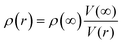
,
31 where
ρ(∞) and
V(∞) are the mass density and lattice volume for the bulk value. The bulk density is given by

, where the average atomic mass
M for In
0.53Ga
0.47As can be calculated as:
43| |  | (28) |
Hence,
Y = 1 and
X = 0.47, and the average atomic masses for In, Ga, and As are abbreviated as
MIn,
MGa, and
MAs, respectively. These are calculated from the relation

where
ci is the natural abundance of the isotope composition and
Mi is the
ith isotope atomic mass, with values of 60.107%, 39.89%, 4.33%, 95.67%, and 100% for
69Ga,
71Ga,
113In,
115In, and
75As, respectively.
35 Accordingly, their average atomic mass is equal to 139.95 × 10
−27 kg. The size-dependent melting temperature
Tm0(
r) is given by:
| | 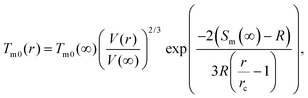 | (29) |
where for In
0.53Ga
0.47As,
Tm0(∞) is 1373.15 K.
54 According to
eqn (20), the dependence of both bulk state, the thick film in this case, and nanosize melting temperature on pressure is calculated as shown in
Fig. 3 (
Fig. 3–11 in Appendix A).
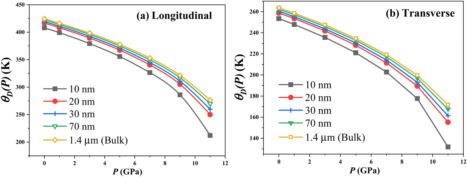
At the nanoscale, the Debye temperature, denoted as θD, is key to understanding atomic vibrations in lattice structures. It is calculated using Lindemann's formula:  . This formula also applies to the pressure dependence of θD for both bulk and nanosize materials:29
| | 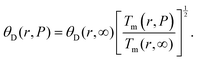 | (30) |
Fig. 4 shows the nanosize Debye temperature–pressure dependence of In
0.53Ga
0.47As. Phonon group velocity in nanofilms (
v(
r)) is derived from Debye temperature
θD(
r) proportionality:

,
28 with
v(∞) being 4260 m s
−1 for longitudinal and 2981 m s
−1 for transverse branches.
55 This relationship is modified for pressure dependence (
Fig. 5):
| |  | (31) |
These calculations are also utilized for zero-pressure size-dependent parameters for both thick (bulk state) and nanofilm thicknesses, as detailed in
Tables 1 and 2.
Table 2 Calculated parameters for In0.53Ga0.47As in both its thick (bulk) and nanofilms
| Parameters |
Thick films 1.4 μm (bulk) |
Nanofilm thickness |
| 70 nm |
30 nm |
20 nm |
10 nm |
|
f
sl (J m−2) |
6.30066 |
6.14814 |
5.94479 |
5.76818 |
5.24622 |
|
H
m (kJ mol−1) |
40.8304 |
40.6086 |
40.3077 |
40.0397 |
39.2079 |
|
σ
sl (J m−2) |
1.67367 |
1.62881 |
1.56884 |
1.5169 |
1.3644 |
|
S
vib (J mol−1 K−1) |
21.42 |
21.1963 |
20.8895 |
20.6138 |
19.7435 |
|
S
m (J mol−1 K−1) |
29.734 |
29.5054 |
29.1986 |
28.9229 |
28.0526 |
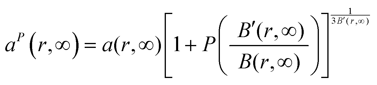
Lattice contraction in bulk (thick film) and nanosizes, due to pressure aP(r,∞), is described by the Murnaghan equation:25
| |  | (32) |
For In
0.53Ga
0.47As semiconductor nanofilms and bulk thickness,
a(
r,∞) is the zero-pressure lattice parameter, and (
aP(
r,∞)) is the pressured lattice parameter, while
B′ determines the first derivative of the bulk modulus. This investigation uses the Murnaghan equation to find that lattice parameter density, and volume decrease with increasing pressure. Changes in pressure affect the size, shape, and bulk modulus (
B) of nanoscale solids, indicating material resistance and hardness.
56,57 The formula for the first derivative of the bulk modulus for cubic materials at ambient pressure is specified:
32
. When pressure derivatives are equal, the first derivative of the bulk modulus is given by the free-volume equation:
32
, for
γth =
γave. In this work, the first derivatives of the bulk moduli for bulk thickness and its corresponding nanoscales are derived as follows:
| |  | (33) |
Then according to
eqn (32), the bulk and nanoscale lattice parameter and volume dependence on pressure are as shown in
Fig. 6. The average Gruneisen parameter
γave in
eqn (33) is influenced by nanoscale size and pressure, calculated as:

.
51 Rice
26 derived an equation for the pressure-dependent Gruneisen parameter (
γP(∞)), which is:

; this equation accounts for pressure effects on the lattice volume of nanoscale solids.
| | 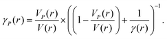 | (34) |
The term
VP(
r) indicates the effect of pressure on nanoscale lattice volume and is estimated by:
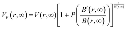
.
Fig. 7 illustrates how this impacts the Gruneisen parameters for both thick (bulk) and nanofilm materials.
Based on eqn (1)–(34), pressure influences the thermodynamic and structural parameters in the LTC-modified equation for both bulk (thick) and nanofilms, as depicted in Fig. 1.
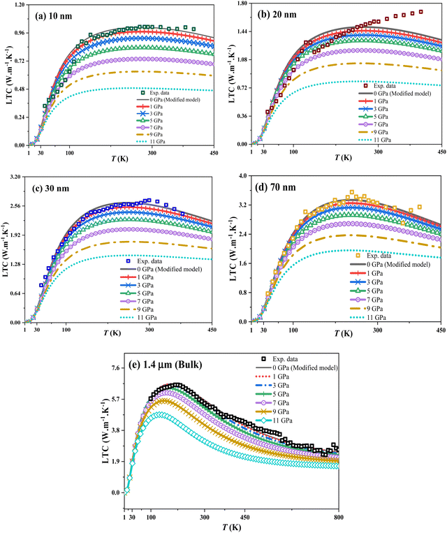 |
| | Fig. 1 LTC of In0.53Ga0.47As alloy nanofilms and bulk dependent on temperature under hydrostatic pressure from 0 to 11 GPa for (a) 10 nm, (b) 20 nm, (c) 30 nm, and (d) 70 nm, and (e) 1.4 μm bulk state, respectively, with experimental data for nanofilm thicknesses obtained from ref. 5, and for bulk (thick) from ref. 20. | |
3. Results and discussion
In LTC calculations for bulk and nanofilms, parameters such as lattice volume, Debye temperature, and group velocity are derived from eqn (20)–(34). Other parameters, like surface roughness and electron concentration, are determined by fitting to the experimental data5,20 at 0 GPa. Excluding dislocations, the concentration of imperfections, such as impurities (Nimp) and electrons (Ne), remains constant across nanosizes and under varying pressures; these values, along with size- and pressure-dependent parameters, eqn (20)–(34), cause modifications in this model, specifically tailored to the properties of In0.53Ga0.47As nanofilms, where (Ne = 0.8 × 1025 m−3) and (Nimp = 0.069 × 10²³ m−3), and these values are obtained from the fitting process to the experimental data5,20 of LTC for phonon–electron and phonon-impurity scattering rates, which are inserted into (τL(T)ph–e)−1 and (τL(T)M)−1 in eqn (10).
New values for the first derivative, appropriate for In0.53Ga0.47As nanofilms, have been determined through a fresh derivation of the nanomaterial form (refer to Table 1). This approach was initially utilized by Hofmeister in 2002 for bulk materials.32
Fig. 1 illustrates how hydrostatic pressure affects the LTC of In0.53Ga0.47As nanofilms and bulk (thick film) with a thickness range from 10 nm to 1.4 μm, highlighting phonon-based heat transfer in this semiconductor alloy.
At low temperatures, phonon wavelengths match the sample size, affecting boundary scattering. As temperature rises, LTC peaks and is influenced by imperfections like dislocations. Electron numbers and impurity concentrations remain unchanged despite size reduction. At higher temperatures, energetic lattice vibrations and short-wavelength phonons (via the umklapp process) scatter with the crystal lattices, impacting LTC, as depicted in Fig. 1a–e. Fig. 1a–e show that hydrostatic pressure decreases LTC across all temperatures for In0.53Ga0.47As nanofilms (10–70 nm) and bulk (1.4 μm). At low temperatures (1–30 K), phonons carry minimal thermal energy, making LTC less pressure-dependent. Boundary scattering, influenced by pressure, temperature, and size, is the key factor here. At the nanoscale, phonons are disrupted, and while their excitation energies rise with temperature, pressure diminishes this effect. Pressure effects on LTC are attributed to lattice rearrangement and reduced dislocation lines, especially in 10 nm nanofilms, lowering the LTC peak and increasing scattering, which diminishes the right-side peak of the LTC curve. Increased pressure leads to higher lattice scattering at sample boundaries, reducing phonon group velocities (Fig. 5); the effects are shown in Fig. 8(a) and (b), and both are obtained from the boundary scattering rate in the nanofilm:  , where
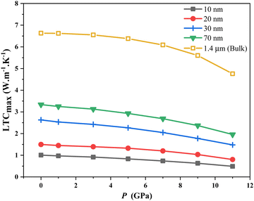
  lc is the Casimir length, and l is the sample size,40 which at 0 GPa equals to 2.61, 2.62, 2.63, 2.64, and 2.8 μm for 10, 20, 30, 70 nm, and 1.4 μm as the bulk, respectively. Surface roughness (ε) ranges from 0 to 1, with ε = 0 for bulk thickness (complete diffusion) and ε = 1 for nanofilms (total reflection). For nanofilms of 10, 20, 30, and 70 nm, the ε values are 0.089, 0.076, 0.069, and 0.054, respectively. Phonon velocities decrease with pressure, more so in thinner films, affecting the In0.53Ga0.47As nanofilms’ LTC. Fig. 8(a) and (b) illustrate the inverse relationship between sample thickness and boundary scattering rate. Boundary scattering significantly affects thermal resistivity, more so in strained samples (10 nm). Hydrostatic pressure modifies this rate, reducing LTC, especially at low to intermediate temperatures. It also limits the phonon wavelengths, increasing scattering effects. Despite fewer dislocations, pressure impacts LTC reduction, as shown in Fig. 8(c). From the dislocation scattering rate formula, the ND (dislocation concentration) values are 4.97 × 10¹⁷, 4.53 × 10¹⁷, 4.27 × 10¹⁷, 3.75 × 10¹⁷ and 1.84 × 10¹⁷ m−2 for 10, 20, 30, 70 nm, and 1.4 μm (thick) bulk, respectively, and they are used to fit LTC to the reported experimental data. The basic assumption is that at intermediate temperatures, boundary scattering has a minor role, while lower dislocation concentration becomes the main factor in thermal energy transfer under pressure. Strained lattices scatter high-energy phonons, affecting LTC as the atom distances decrease under pressure. Smaller sizes see more impact, likely from bond weakening. The effect of pressure on smaller nanosize elucidates the influence of LTC in thinner films (Fig. 1), which is convenient with ref. 58 and 59. LTC reduction with nanosize decrease is evident in In0.53Ga0.47As nanofilms (Fig. 9). Despite pressure-reducing dislocations, LTCmax declines due to boundary scattering's greater influence compared to dislocations.
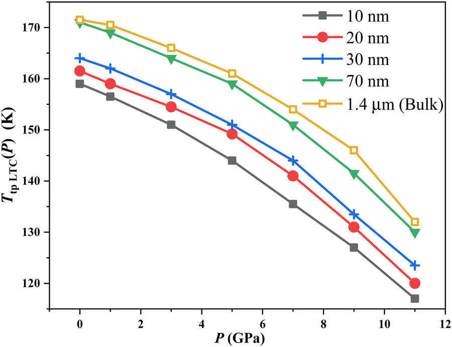
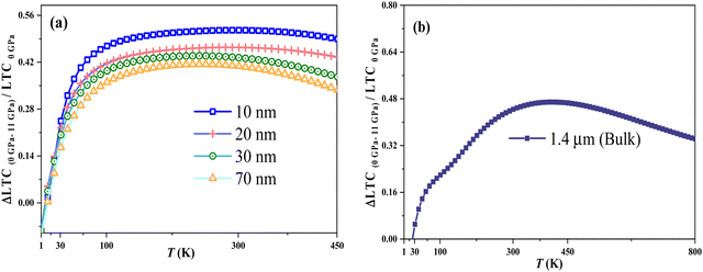
To investigate the pressure's impact on the thermal properties of the In0.53Ga0.47As alloy's nanosize, the LTC at the turning point temperature due to pressure, Ttp LTC(P), is plotted against pressure in Fig. 10. The LTC at this point is influenced by boundary and lattice dislocation at low and intermediate temperatures. As size compression increases, so does boundary scattering, which outweighs the reduction in lattice dislocations. Increased pressure significantly lowers LTC in thinner films due to a greater reduction in lattice structure and volume, with a pronounced effect in smaller nanofilms, as shown in Fig. 2 and 11.
 |
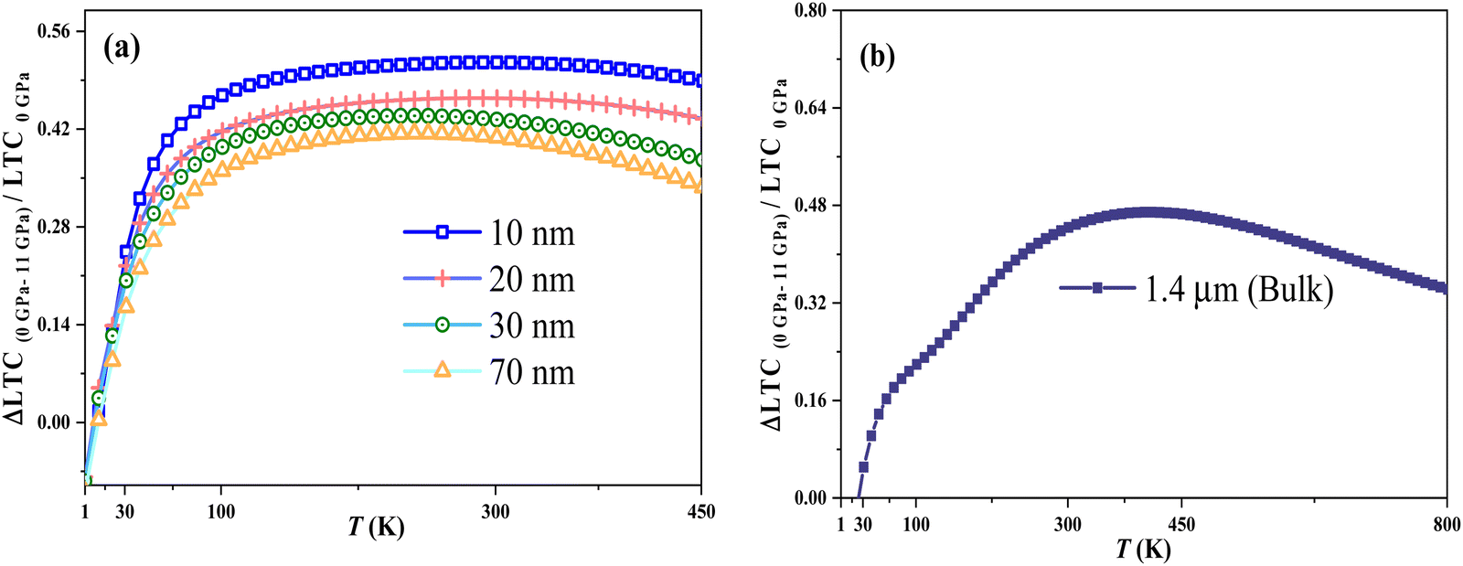
| | Fig. 2 The dependence of (ΔLTC/LTC)P on nanofilm thickness at 300 K. | |
4. Conclusions
(1) It is expected from this work that the concentrations of both impurities and electrons will remain the same as those in the bulk, unchanged by both effects of nanoscale dimensions and pressure.
(2) Clapeyron, Murnaghan and Post equations were successfully applied within the modified Debye–Callaway model to assess the effects of hydrostatic pressure on the film's lattice thermal conductivity (LTC), considering surface energy and stress.
(3) At a low temperature range, the reduced LTC due to pressure (ΔLTC/LTC)P is a strongly temperature-dependent parameter that approaches its minimum value at temperatures above T = 100 K. It is also a size-dependent parameter, increasing from its minimum value at low temperatures to a maximum value at room temperature.
(4) The insights gained in this work could be crucial for optimizing the thermal properties of nano thermoelectric devices, potentially improving their functionality and efficiency.
Data availability
The data that support the findings of this study are available from the corresponding author upon reasonable request.
Conflicts of interest
The authors have no conflicts to disclose.
Appendix
Fig. 3–11.
 |
| | Fig. 3 Melting temperature as a function of pressure for In0.53Ga0.47As films up to 11 GPa. | |
 |
| | Fig. 4 (a) Longitudinal and (b) transverse modes for Debye temperature as a function of pressure for In0.53Ga0.47As films up to 11 GPa. | |
 |
| | Fig. 5 Phonon group velocity dependent on pressure for In0.53Ga0.47As alloy films for (a) longitudinal and (b) transverse modes, for both thick (bulk) and nanofilms. | |
 |
| | Fig. 6 Pressure-dependent (a) lattice parameter, and (b) lattice volume, for In0.53Ga0.47As alloy films of up to 11 GPa. | |
 |
| | Fig. 7 Gruneisen parameter dependence on pressure for In0.53Ga0.47As alloy films for both modes (a) longitudinal, and (b) transverse. | |
 |
| | Fig. 8 Δ(τBoundary)−1 as a function of pressure in (a) and (b), Δ(τDislocation)−1/(τDislocation)−1 in (c) with different thicknesses of 10, 20, 30, and 70 nm and the bulk state for the In0.53Ga0.47As alloy. | |
 |
| | Fig. 9 LTCmax as a function of pressure for In0.53Ga0.47As nanofilms with different thicknesses of 10, 20, 30, and 70 nm and bulk (thick). | |
 |
| | Fig. 10 The turning point temperature for LTC as a function of pressure for In0.53Ga0.47As alloy films. | |
 |
| | Fig. 11 (ΔLTC/LTC)P as a function of temperature for In0.53Ga0.47As alloy with different thicknesses of (a) 10, 20, 30, and 70 nm, and (b) bulk state. | |
Acknowledgements
Thanks go to I. N. Qader for his assistance, and the authors would like to acknowledge the financial support under grant no. (3/1/6464-992020) from the College of Science at Salahaddin University-Erbil in Kurdistan Region, Iraq.
References
- M. S. Gudiksen, L. J. Lauhon, J. Wang, D. C. Smith and C. M. Lieber, Nature, 2002, 415, 617–620 CrossRef CAS PubMed.
- Y. Dong, B.-Y. Cao and Z.-Y. Guo, Phys. E, 2015, 66, 1–6 CrossRef CAS.
- L. Zhu, X. Tang, J. Wang and Y. Hou, AIP Adv., 2019, 9, 015024 CrossRef.
- R. Chau, B. Boyanov, B. Doyle, M. Doczy, S. Datta, S. Hareland, B. Jin, J. Kavalieros and M. Metz, Phys. E, 2003, 19, 1–5 CrossRef.
- J. Kim, H. Kim, M. Emin Kilic, C. Gayner, R. Koltun, H. Park, A. Soon, J. Bowers, C. Palmstrøm and W. Kim, J. Appl. Phys., 2018, 123, 245103 CrossRef.
- G. Chen, Int. J. Therm. Sci., 2000, 39, 471–480 CrossRef CAS.
- A. San-Miguel, Chem. Soc. Rev., 2006, 35, 876–889 RSC.
- P. McMillan, High Press. Res., 2003, 23, 7–22 CrossRef CAS.
- B. I. Sharma, J. Appl. Fundam. Sci., 2015, 1, 7 Search PubMed.
- F. Gao, L. Wen, X. Zhang, Y. Guan, J. Li, S. Zhang and G. Li, Thin Solid Films, 2015, 589, 32–37 CrossRef CAS.
- T. Pearsall, IEEE J. Quantum Electron., 1980, 16, 709–720 CrossRef.
- G. Yang and S.-J. Park, Materials, 2019, 12, 2003 CrossRef CAS PubMed.
- D. Bimberg, N. Kirstaedter, N. Ledentsov, Z. I. Alferov, P. Kop’ev and V. Ustinov, IEEE J. Sel. Top. Quantum Electron., 1997, 3, 196–205 CrossRef CAS.
- T. Pearsall, M. Piskorski, A. Brochet and J. Chevrier, IEEE J. Quantum Electron., 1981, 17, 255–259 Search PubMed.
- S. Anthony, Ars Technica, 2015, 23, 201 Search PubMed.
- E. Dong, B. Liu, Q. Dong, X. Shi, X. Ma, R. Liu, X. Zhu, X. Luo, X. Li and Y. Li, Phys. B, 2020, 595, 412344 CrossRef CAS.
- H. H. Karim, M. Omar and I. N. Qader, Phys. B, 2022, 640, 414045 CrossRef CAS.
- M. Hamarashid, M. Omar and I. N. Qader, Silicon, 2022, 1–10 Search PubMed.
- I. N. Qader, D. M. Mamand, H. H. Rasul, B. J. Abdullah and M. S. Omar, Iran. J. Sci. Technol., Trans. A: Sci., 2022, 1–14 Search PubMed.
- W. Kim, S. L. Singer, A. Majumdar, J. M. Zide, D. Klenov, A. C. Gossard and S. Stemmer, Nano Lett., 2008, 8, 2097–2099 CrossRef CAS PubMed.
- A. Cherstvy and A. Kornyshev, J. Phys. Chem. B, 2005, 109, 13024–13029 CrossRef CAS PubMed.
-
M. Akaogi, in Encyclopedia of Geochemistry: A Comprehensive Reference Source on the Chemistry of the Earth, ed. W. M. White, Springer International Publishing, Cham, 2018, pp. 262–263 DOI:10.1007/978-3-319-39312-4_301.
- C. Yang and Q. Jiang, Scr. Mater., 2004, 51, 1081–1085 CrossRef CAS.
- Q. Jiang and C. Yang, Curr. Nanosci., 2008, 4, 179–200 CrossRef CAS.
- F. D. Murnaghan, Proc. Natl. Acad. Sci. U. S. A., 1944, 30, 244–247 CrossRef CAS PubMed.
- M. Rice, J. Phys. Chem. Solids, 1965, 26, 483–492 CrossRef CAS.
- M. Omar, B. J. Abdullah, A. S. Karim and S. K. Jalal, Silicon, 2023, 1–8 CAS.
- E. J. Post, Can. J. Phys., 1953, 31, 112–119 CrossRef CAS.
- L. Liang and B. Li, Phys. Rev. B: Condens. Matter Mater. Phys., 2006, 73, 153303 CrossRef.
- C. Yang, J. Li and Q. Jiang, Chem. Phys. Lett., 2003, 372, 156–159 CrossRef CAS.
- B. Abdullah, M. Omar and Q. Jiang, Sādhanā, 2018, 43, 1–5 CrossRef CAS.
- A. M. Hofmeister and H.-k Mao, Proc. Natl. Acad. Sci. U. S. A., 2002, 99, 559–564 CrossRef CAS PubMed.
- J.-Y. Wu, P. Huang, Q.-H. Luc, H.-L. Ko, Y.-C. Chiang, H.-C. Yu, M.-Y. Chen and E. Y. Chang, IEEE Trans. Nanotechnol., 2023, 22, 445–448 CAS.
- M. Asen-Palmer, K. Bartkowski, E. Gmelin, M. Cardona, A. Zhernov, A. Inyushkin, A. Taldenkov, V. Ozhogin, K. M. Itoh and E. Haller, Phys. Rev. B: Condens. Matter Mater. Phys., 1997, 56, 9431 CrossRef CAS.
- D. Morelli, J. Heremans and G. Slack, Phys. Rev. B: Condens. Matter Mater. Phys., 2002, 66, 195304 CrossRef.
- J. Zou, J. Appl. Phys., 2010, 108, 034324 CrossRef.
-
D. T. Morelli and G. A. Slack, High thermal conductivity materials, Springer, 2006, pp. 37–68 Search PubMed.
- J. Callaway, Phys. Rev., 1959, 113, 1046 CrossRef CAS.
- G. A. Slack and S. Galginaitis, Phys. Rev., 1964, 133, A253 CrossRef.
- S. Mamand, M. Omar and A. Muhammad, Mater. Res. Bull., 2012, 47, 1264–1272 CrossRef CAS.
- W. Kim, J. Zide, A. Gossard, D. Klenov, S. Stemmer, A. Shakouri and A. Majumdar, Phys. Rev. Lett., 2006, 96, 045901 CrossRef PubMed.
- D. Q. Tran, R. Delgado-Carrascon, J. F. Muth, T. Paskova, M. Nawaz, V. Darakchieva and P. P. Paskov, Appl. Phys. Lett., 2020, 117, 252102 CrossRef CAS.
- S. Mei and I. Knezevic, J. Appl. Phys., 2015, 118, 175101 CrossRef.
- J. Zou and A. Balandin, J. Appl. Phys., 2001, 89, 2932–2938 CrossRef CAS.
- R. People, A. Jayaraman, K. Wecht, D. Sivco and A. Cho, Appl. Phys. Lett., 1988, 52, 2124–2126 CrossRef CAS.
-
Y. A. Goldberg and N. M. Shmidt, Handbook Series on Semiconductor Parameters: Ternary and quaternary A3B5 semiconductors, 1999, vol. 2, p. 62 Search PubMed.
- D. Narducci, G. Cerofolini, M. Ferri, F. Suriano, F. Mancarella, L. Belsito, S. Solmi and A. Roncaglia, J. Mater. Sci., 2013, 48, 2779–2784 CrossRef CAS.
- C. Yang, G. Li and Q. Jiang, J. Phys.: Condens. Matter, 2003, 15, 4961 CrossRef CAS.
- M. Omar, Mater. Res. Bull., 2012, 47, 3518–3522 CrossRef CAS.
- M. Omar, Int. J. Thermophys., 2016, 37, 1–11 CrossRef CAS.
- E. Post, Can. J. Phys., 1953, 31, 112–119 CrossRef CAS.
- M. Omar and H. Taha, Sadhana, 2010, 35, 177–193 CrossRef CAS.
- M. Omar, Mater. Res. Bull., 2007, 42, 961–966 CrossRef CAS.
-
M. S. Shur, Handbook Series on Semiconductor Parameters: Ternary and Quaternary III-V Compounds, World Scientific, 1996, vol. 2 Search PubMed.
-
S. Adachi, Physical properties of III-V semiconductor compounds, John Wiley & Sons, 1992 Search PubMed.
- M. Sarwan and S. Singh, J. Alloys Compd., 2013, 550, 150–158 CrossRef CAS.
- S. Wang and H. Ye, Phys. Status Solidi B, 2003, 240, 45–54 CrossRef CAS.
- H. Luo and L. Zhu, J. Appl. Mech., 2015, 82, 111002 CrossRef.
- L. Zhu and H. Luo, J. Alloys Compd., 2016, 685, 619–625 CrossRef CAS.
|
| This journal is © the Owner Societies 2024 |
Click here to see how this site uses Cookies. View our privacy policy here. 
 * and
M. S.
Omar
* and
M. S.
Omar

 , ħ, kB, T, v and ω are the Planck constant (1.05457 × 10⁻³⁴ J s), Boltzmann's constant (1.38065 × 10⁻²³ m2 kg s−2 K−1), absolute temperature, acoustic phonon group velocity and phonon frequency, respectively. The combined phonon-scattering is denoted by τC(x),38 while τR(x) is the resistive total scattering. Furthermore, both branches of Debye temperature are determined by θL(T)D:35


 , representing the strength of the mass difference interaction, which for In0.53Ga0.47As, is calculated as follows:43


 , and for nanosized films, it is modified to:
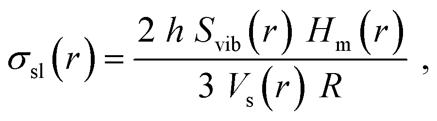
 , for nanofilms, the form is modified to:
 ,51 and its nanosized modification is as in the following:

 .49 Accordingly, the lattice volumes for both bulk and nanosize dependence of cubic zinc blende shape structures including In0.53Ga0.47As are calculated from relations
  and
and 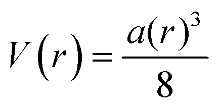 , respectively.52,53 The nanostructure mass density ρ(r) is calculated from the size-dependent lattice volume V(r) of a nanofilm according to
  ,31 where ρ(∞) and V(∞) are the mass density and lattice volume for the bulk value. The bulk density is given by
  , where the average atomic mass M for In0.53Ga0.47As can be calculated as:43
 where ci is the natural abundance of the isotope composition and Mi is the ith isotope atomic mass, with values of 60.107%, 39.89%, 4.33%, 95.67%, and 100% for 69Ga, 71Ga, 113In, 115In, and 75As, respectively.35 Accordingly, their average atomic mass is equal to 139.95 × 10⁻²⁷ kg. The size-dependent melting temperature Tm0(r) is given by:
 . This formula also applies to the pressure dependence of θD for both bulk and nanosize materials:29
 ,28 with v(∞) being 4260 m s−1 for longitudinal and 2981 m s−1 for transverse branches.55 This relationship is modified for pressure dependence (Fig. 5):
 . When pressure derivatives are equal, the first derivative of the bulk modulus is given by the free-volume equation:32
 , for γth = γave. In this work, the first derivatives of the bulk moduli for bulk thickness and its corresponding nanoscales are derived as follows:
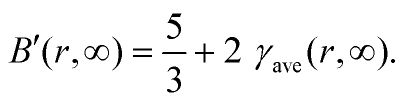
 .51 Rice26 derived an equation for the pressure-dependent Gruneisen parameter (γP(∞)), which is:
  ; this equation accounts for pressure effects on the lattice volume of nanoscale solids.
 . Fig. 7 illustrates how this impacts the Gruneisen parameters for both thick (bulk) and nanofilm materials.

 , where
  lc is the Casimir length, and l is the sample size,40 which at 0 GPa equals to 2.61, 2.62, 2.63, 2.64, and 2.8 μm for 10, 20, 30, 70 nm, and 1.4 μm as the bulk, respectively. Surface roughness (ε) ranges from 0 to 1, with ε = 0 for bulk thickness (complete diffusion) and ε = 1 for nanofilms (total reflection). For nanofilms of 10, 20, 30, and 70 nm, the ε values are 0.089, 0.076, 0.069, and 0.054, respectively. Phonon velocities decrease with pressure, more so in thinner films, affecting the In0.53Ga0.47As nanofilms’ LTC. Fig. 8(a) and (b) illustrate the inverse relationship between sample thickness and boundary scattering rate. Boundary scattering significantly affects thermal resistivity, more so in strained samples (10 nm). Hydrostatic pressure modifies this rate, reducing LTC, especially at low to intermediate temperatures. It also limits the phonon wavelengths, increasing scattering effects. Despite fewer dislocations, pressure impacts LTC reduction, as shown in Fig. 8(c). From the dislocation scattering rate formula, the ND (dislocation concentration) values are 4.97 × 10¹⁷, 4.53 × 10¹⁷, 4.27 × 10¹⁷, 3.75 × 10¹⁷ and 1.84 × 10¹⁷ m−2 for 10, 20, 30, 70 nm, and 1.4 μm (thick) bulk, respectively, and they are used to fit LTC to the reported experimental data. The basic assumption is that at intermediate temperatures, boundary scattering has a minor role, while lower dislocation concentration becomes the main factor in thermal energy transfer under pressure. Strained lattices scatter high-energy phonons, affecting LTC as the atom distances decrease under pressure. Smaller sizes see more impact, likely from bond weakening. The effect of pressure on smaller nanosize elucidates the influence of LTC in thinner films (Fig. 1), which is convenient with ref. 58 and 59. LTC reduction with nanosize decrease is evident in In0.53Ga0.47As nanofilms (Fig. 9). Despite pressure-reducing dislocations, LTCmax declines due to boundary scattering's greater influence compared to dislocations.