
Two-dimensional SPdAZ2 (A = Si, Ge; Z = N, P, As) monolayers with an intrinsic electric field for high-performance photocatalysis†
Zhen
Gao
 a,
Yao
He
*a and
Kai
Xiong
*b
a,
Yao
He
*a and
Kai
Xiong
*b
aDepartment of Physics, Yunnan University, Kunming 650091, People's Republic of China. E-mail: yhe@ynu.edu.cn
bMaterials Genome Institute, School of Materials and Energy, Yunnan University, Kunming 650091, P. R. China. E-mail: xiongkai@ynu.edu.cn
First published on 6th December 2023
Abstract
Two-dimensional materials exhibiting exceptional photocatalytic properties and a low carrier recombination rate have garnered significant attention. However, such attributes are relatively scarce among conventional two-dimensional materials. Two-dimensional Janus materials, owing to their intrinsic electric field, hold substantial promise in the realm of photocatalysis. In this study, we conducted a comprehensive investigation of the electronic, optical and photocatalytic properties, as well as the carrier mobility of SPdAZ2 (A = Si, Ge; Z = N, P, As) monolayers employing first-principles calculations. Employing the HSE06 hybrid density functional, we discovered that all six structures exhibit semiconductor characteristics with indirect band gaps under equilibrium conditions. Notably, SPdSiP2, SPdSiAs2, and SPdGeP2 monolayers displayed advantageous band edge positions, facilitating effective photocatalytic water decomposition. Furthermore, we computed the carrier mobility of SPdAZ2 monolayers, revealing significant variations in the electron and hole mobility along the same direction, which enhances the effective separation of electrons and holes. Finally, we explored the impact of biaxial strain and an applied electric field on the electronic properties, photocatalysis, and light absorption of SPdAZ2 monolayers. These compelling features underscore the broad potential applications of SPdAZ2 (A = Si, Ge; Z = N, P, As) monolayers in the realm of photocatalytic water decomposition.
1. Introduction
Hydrogen, generated through the photocatalytic decomposition of water, serves as a desirable and clean energy source with the potential to address pressing environment pollution and energy shortages. Since 1972, when Fujishima and Honda first uncovered the exceptional photocatalytic water decomposition capabilities of TiO2 semiconductors, semiconductor-based photocatalysts have garnered widespread attention.1 However, to date, only a select few semiconductor materials have managed to meet the necessary conditions for water decomposition. In broad terms, the efficient photocatalytic decomposition of water into hydrogen relies on several key factors: strong optical capture, efficient carrier separation and rapid migration, and favorable hydrogen and oxygen evolution reactions (HER and OER). Furthermore, for a photocatalyst to be widely employed, its band gap must be equal to or greater than 1.23 eV, with the redox potential falling within the band edge position. Meeting these conditions enables the breakdown of water into O2 and H2.2,3 Consequently, much effort has been made in the search for semiconductor materials displaying outstanding photocatalytic performance.4–7 Unfortunately, most three-dimensional (3D) photocatalysts predominantly absorb ultraviolet light, and their low carrier mobility leads to a high carrier recombination rate, hindering the full utilization of absorbed light.8–11 Furthermore, 3D semiconductors typically exhibit a low surface to volume ratio, resulting in an inadequate number of reaction sites. Therefore, the feeble redox reactions stemming from these limitations impede the broader industrial application of 3D photocatalysts.12–14Recent studies have highlighted the outstanding optical absorption properties, high carrier mobility, and ample reaction sites exhibited by two-dimensional (2D) materials, positioning them as promising candidates for photocatalysis. Therefore, 2D monolayers have played a crucial role in the realm of photocatalytic water decomposition.15–20 One such 3D material, g-C3N4, has garnered significant research interest as a representative 2D photocatalyst.21 However, a limitation of the g-C3N4 monolayer lies in its reliance on a sacrificial donor during the photocatalytic process to achieve water decomposition, rendering it inactive.3 Therefore, the quest for 2D photocatalysts capable of water splitting has received considerable importance. Encouragingly, research has revealed that 2D materials with inherent polarization exhibit a reduced carrier recombination rate, thereby enhancing their ability to decompose water.22 In 2014, Yang's research team functionalized the surface of bilayered boron nitride, resulting in a polar 2D structure. This innovation alleviated the band gap limitation and demonstrated that 2D polarized materials possess appropriate redox potentials and favorable light absorption energies.23 Subsequently, in 2017, the successful fabrication of MoSSe monolayers in experiments prompted extensive research into 2D Janus transition metal dihalide (MXY, M = transition metal; X, Y = S, Se, Te; X ≠ Y) monolayers. These investigations unveiled their exceptional photocatalytic performance, positioning them as promising photocatalysts for water splitting.24–27
In recent years, experimental synthesis efforts have successfully produced various phases of In2X3 (X = S, Se, Te) monolayers, revealing their remarkable photosensitivity through research efforts.28–31 Among these phases, α-In2X3, distinguished by its asymmetric structure, has been identified as possessing both in-plane and out-of-plane piezoelectric properties32 and ferroelectric properties.29 This makes it an ideal choice for application in sensors, actuators, energy conversion, and data storage devices. Fu et al. conducted a comprehensive investigation into 2D M2X3 (M = Al, Ga, In; X = S, Se, Te) monolayers, with carrier distribution, transfer, light absorption, and solar to hydrogen (STH) conversion efficiency, showcasing their potential as photocatalysts.33 Due to the remarkable performance of M2X3 (M = Al, Ga, In; X = S, Se, Te) monolayers and the potential of Janus materials in the field of photocatalysis, researchers have delved into the exploration of 2D Janus In2X2Y (X, Y = S, Se, Te; X ≠ Y) monolayers. Their findings have revealed that these Janus structures exhibit exceptional photocatalytic performance, along with significant in-plane and out-of-plane piezoelectric responses.34 Building on this discovery, a series of 2D Janus M2X2Y monolayers (M = Al, Ga, In, Sb, Ge, Sn; X, Y = O, S, Se, Te; X ≠ Y) were investigated, and the results demonstrated that these structures continue to display outstanding photocatalytic and piezoelectric properties.34–36 Recently, there has been successful experimental synthesis of a novel seven-atom-layer structure known as MoSi2N4 using a chemical vapor deposition (CVD) method.37 Upon close examination of its atomic structure, it was observed that the MoSi2N4 monolayer comprises a MoN2 layer situated between two Si-N bilayers.37 Subsequent research has revealed that under environmental conditions, the MoSi2N4 monolayer exhibits semiconductor properties, featuring a band gap of approximately 2.0 eV, and demonstrates robust stability.38 The MoSi2N4 monolayer exhibits numerous outstanding characteristics, including a significant light absorption coefficient39 and a high thermal conductivity coefficient.40 These findings have opened up potential applications in the fields of photocatalysis and optoelectronic devices. Leveraging the exceptional physical and chemical properties of the MoSi2N4 monolayer, researchers have embarked on the prediction and extensive exploration of similar 2D materials belonging to MA2Z4 (M = transition metal; A = Si or Ge; Z = N, P, As) through density functional theory (DFT) simulations.41–44 These findings have shed light on promising materials with various potential applications. Building on the insights gained from theoretical and experimental investigations of the MA2Z4 family materials, as well as the successful synthesis and excellent properties observed in 2D Janus structures, R T. Sibatov et al. introduced a novel asymmetric 2D Janus structure called XMoSiN2. This structure is achieved by removing one side of SiN from the MoSi2N4 monolayer and substituting the remaining N atoms on that side with sulfur group X atoms (sulfur, selenium, or tellurium).45 Consequently, Janus structures based on the MA2Z4 family of innovative penta-atomic layers, such as XMAZ2 (X = O, S, Se, Te; M = Cr, Mo, W, Ti; A = Si, Ge; Z = N, P, As), have been theoretically predicted to exhibit exceptional properties.45–51 These materials showcase outstanding photocatalytic, piezoelectric, Rashba-type spin splitting, and tunable electronic properties. As a result, they hold significant potential for wide-ranging applications in electronic and optoelectronic devices. Similar to Mo and W atoms, the Pd atom is classified as a d-block transition metal and is highly regarded as a precious metal.52 These metals play important roles as catalysts in various industrial processes,53 and their nanoparticles find widespread use in chemical catalytic applications.54 In recent years, researchers have made significant strides in the field of 2D materials, particularly in the synthesis of 2D Pd-based dihalide compounds such as PdSe2.55,56 These compounds have been proposed for a range of applications, including serving as catalysts for the hydrogen evolution reaction, components in field-effect transistors (FETs), and materials for photodetectors.56 Additionally, stable PdN2 monolayers with distinctive properties have been predicted using group optimization-based structural research methods.57 Furthermore, stable layered PdX2 (X = P, As) compounds have been explored theoretically and identified as direct band gap semiconductors, exhibiting good carrier transport performance and high thermoelectric efficiency.58 These advancements highlight the promising future of 2D Pd-based materials across various technological and scientific domains.
Given the underexplored potential of various Janus structures within the MA2Z4 family for efficient photocatalytic water decomposition, we initiated the construction and investigation of these structures, focusing on their physical properties in the context of penta-atomic layer Janus materials. Motivated by the unique penta-atomic Janus structure and the growing demand for efficient photocatalysts, our research systematically delves into the stability and electronic, optical and photocatalytic properties of 2D Janus SPdAZ2 (A = Si, Ge; Z = N, P, As) monolayers using first principles calculations. Our findings confirm the dynamic, thermal and mechanical stability of these SPdAZ2 monolayers. Furthermore, employing the HSE06 hybrid functional, we determined that all six structures exhibit indirect band gap semiconductor properties. Next, we investigated the optical and photocatalytic properties of these six structures under biaxial strain and an external electric field in the equilibrium state. Our research uncovered that under equilibrium conditions, SPdSiP2, SPdSiAs2, and SPdGeP2 monolayers exhibit favorable band edge positions conducive to both water oxidation and reduction reactions, particularly under acidic conditions (pH = 0). Conversely, SPdSiN2, SPdGeN2, and SPdGeAs2 can only facilitate water oxidation reactions under these conditions. Under neutral conditions (pH = 7), the use of all six structures is limited to supporting water oxidation reactions, with the reduction capability diminished. Moreover, our calculation of carrier mobility substantiates that these six semiconductor materials exhibit reduced carrier recombination rates. When subject to strain and an applied electric field, we observed that the photocatalytic and absorption properties of SPdSiN2 and SPdGeN2 monolayers cannot be adjusted. The photocatalytic and absorption capabilities of SPdGeP2 and SPdGeAs2 monolayers can be adjusted simultaneously under biaxial strain and an applied electric field. In contrast, the photocatalytic and absorption properties of SPdSiP2 and SPdSiAs2 monolayers can only be modified under strain conditions, while there is almost no change under the influence of an external electric field. Therefore, our findings successfully predict the promising potential of Janus SPdAZ2 (A = Si, Ge; Z = N, P, As) monolayers in the field of photocatalysis.
2. Computational methods
The Vienna ab initio simulation package (VASP)59 was used for the density functional theory (DFT) calculations and the projector augmented wave method (PAW) approach60 was applied to represent the ion–electron interaction. The electronic exchange–correlation functional was treated using the generalized gradient approximation (GGA) proposed by the Perdew–Burke–Ernzerhof (PBE) functional.61 The energy cutoff of the plane waves was set to 400 eV. The structures were fully relaxed until the maximum force on each atom was less than 0.005 eV Å−1. The energy convergence criterion for the self-consistent calculations was set to 10−6 eV. 12 × 12 × 1 and 24 × 24 × 1 Monkhorst–Pack k-point grids were used for geometry optimization and self-consistent calculation, respectively. The Heyd–Scuseria–Ernzerhof (HSE06) functional is chosen to obtain a more accurate band gap for materials.62 A vacuum slab of at least 20 Å in the z direction was adopted to avoid artificial interactions between the neighboring layers. The phonon dispersion was computed by using the Phonopy code63 within the density functional perturbation theory (DFPT).64Ab initio molecular dynamics (AIMD) simulations were performed at 300 K within 5 ps (each time step of 1 fs) to evaluate the thermodynamically stability of 2D Janus SZrAZ2 (A = Si, Ge; Z = N, P, As). The initial configuration was taken from a 5 × 5 × 1 supercell containing 25 S atoms, 25 Pd atoms, 25 A atoms and 50 Z atoms. The strain is defined as ε = (a − a0)/a0, where a is the lattice constant at strained states and a0 represents that for the strain-free state.3. Results and discussion
3.1. Atomic structures and structural stability
The optimized lattice structures of SPdAZ2 (A = Si, Ge; Z = N, P, As) are shown in Fig. 1. From Fig. 1 (b), it is evident that single layered SPdAZ2 (A = Si, Ge; Z = N, P, As) comprises five atomic layers, each consisting of a single element. The atomic arrangement order of SPdAZ2 monolayers is S–Pd–Z–A–Z. Consequently, we constructed six structures, including SPdSiN2, SPdSiP2, SPdSiAs2, SPdGeN2, SPdGeP2, and SPdGeAs2 monolayers. Detailed structural parameters can be found in Table 1. From Table 1, we can see that as the atomic radius increases gradually, both the lattice constant and bond length progressively increase. This trend is consistent with previous research findings.34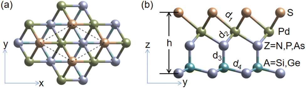 | ||
| Fig. 1 (a) Top and (b) side views of the Janus SPdAZ2(A = Si, Ge; Z = N, P, As) monolayers. | ||
| Phase | a | d 1 | d 2 | d 3 | d 4 | h | E coh |
|---|---|---|---|---|---|---|---|
| SPdSiN2 | 3.082 | 2.336 | 2.090 | 1.733 | 1.835 | 4.792 | −5.984 |
| SPdSiP2 | 3.581 | 2.451 | 2.323 | 2.247 | 2.289 | 5.603 | −4.855 |
| SPdSiAs2 | 3.684 | 2.473 | 2.417 | 2.376 | 2.394 | 5.887 | −4.479 |
| SPdGeN2 | 3.218 | 2.328 | 2.117 | 1.889 | 1.937 | 4.856 | −5.401 |
| SPdGeP2 | 3.630 | 2.461 | 2.331 | 2.342 | 2.355 | 5.726 | −4.589 |
| SPdGeAs2 | 3.817 | 2.499 | 2.446 | 2.476 | 2.484 | 5.862 | −4.280 |
To assess the energy stability of Janus SPdAZ2 (A = Si, Ge; Z = N, P, As) monolayers, we calculated the cohesive energy (Ecoh) of these structures using the formula given below to determine their feasibility:
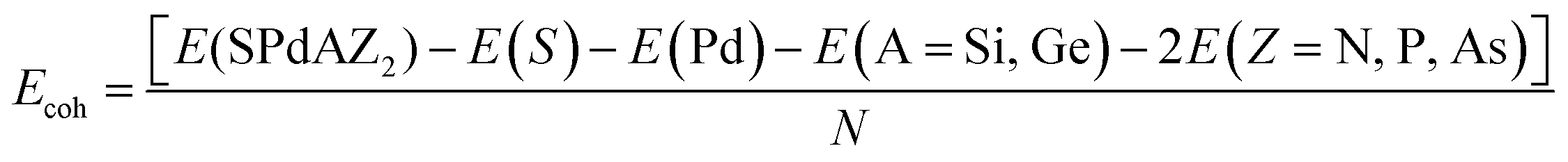
Next, we conducted an analysis of the phonon dispersion for SPdAZ2 monolayers to assess their dynamic stability. In essence, a material is considered dynamically stable when its vibration spectrum exclusively comprises positive frequencies. The calculated phonon dispersion diagrams for SPdAZ2 monolayers are depicted in Fig. 2. Our findings reveal that the vibrational spectra of these six structures, as observed within the first Brillouin zone, solely consist of positive frequencies. This signifies that SPdAZ2 (A = Si, Ge; Z = N, P, As) monolayers exhibit dynamic stability. Furthermore, to assess thermal stability, we employed relatively large 5 × 5 supercells for the SPdAZ2 (A = Si, Ge; Z = N, P, As) monolayers and conducted AIMD simulations at 300 K within 5 ps. The results presented in Fig. S1 (ESI†) demonstrate that there were no instances of chemical bond breakage or structural phase transitions in these six structures. Additionally, the energy exhibited minimal fluctuations within a narrow range of approximately 0.1 eV per atom. These findings collectively affirm the thermal stability of SPdAZ2 (A = Si, Ge; Z = N, P, As) monolayers. To investigate the mechanical stability of these structures, we analyzed the elastic constant (Cij) using the Born Huang's mechanical stability criterion.67 In the case of 2D materials, there are typically four independent Cij, namely C11, C22, C12, and C66. However, due to the central hexagonal symmetry of the 2D Janus SPdAZ2 (A = Si, Ge; Z = N, P, As) monolayers, we have the relations C11 = C22 and C66 = (C11 − C12)/2. Therefore, only two independent parameters, C11 and C12, are required. Our calculations yielded the results of Cij for SPdAZ2 (A = Si, Ge; Z = N, P, As) monolayers, as presented in Table 2. The calculation results demonstrate that all 2D Janus SPdAZ2 (A = Si, Ge; Z = N, P, As) monolayers meet the Born Huang's mechanical stability criterion: C11 > 0 and C112 > C122, indicating their mechanical stability. Considering the close relationship between Young's modulus (Y2D), Poisson's ratio (ν) and Cij, we calculated Y2D and ν using the following formulas:
| Y2D = (C112 − C122)/C11 |
| ν = C12/C11 |
 | ||
| Fig. 2 Phonon dispersions of the (a) SPdSiN2, (b) SPdSiP2, (c) SPdSiAs2 (d) SPdGeN2, (e) SPdGeP2 and (f) SPdGeAs2 monolayers, respectively. | ||
| Phase | C 11 | C 12 | C 66 | Y 2D | ν |
|---|---|---|---|---|---|
| SPdSiN2 | 95.667 | 21.065 | 37.301 | 182.057 | 0.220 |
| SPdSiP2 | 62.310 | 16.768 | 22.771 | 115.595 | 0.269 |
| SPdSiAs2 | 52.114 | 13.684 | 19.215 | 97.042 | 0.263 |
| SPdGeN2 | 88.113 | 25.906 | 31.104 | 160.993 | 0.294 |
| SPdGeP2 | 61.616 | 24.669 | 18.474 | 103.479 | 0.400 |
| SPdGeAs2 | 45.251 | 11.805 | 16.723 | 84.343 | 0.261 |
The specific results can be found in Table 2. Upon examination, we observe that the Y2D values of these structures fall within the range of 84.343 to 180.057 GPa nm. These values are smaller than those of 2D MoS2 (330 GPa nm)68 but greater than the values for phosphorene (23.0 GPa nm).69 In summary, SPdAZ2 (A = Si, Ge; Z = N, P, As) monolayers exhibit favorable mechanical stability.
3.2. Electronic properties
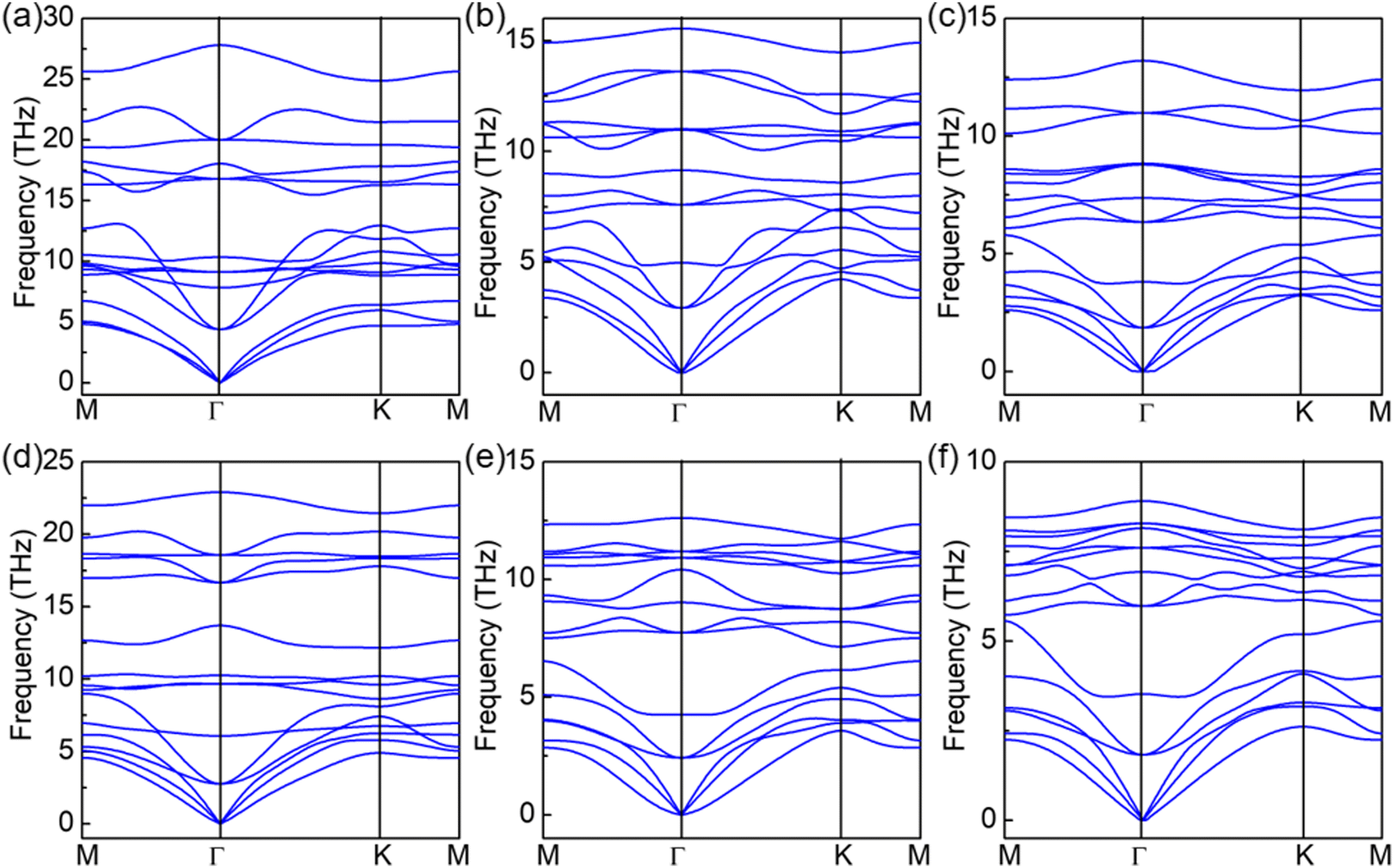
Now, we turn to studying the electronic properties of SPdAZ2 (A = Si, Ge; Z = N, P, As) monolayers. It is well-known that the PBE functional generally underestimates the band gap by about 30%, and the band gap calculated using the HSE06 method has an acceptable accuracy.70 Therefore, we employed the HSE06 hybrid functional to calculate the band structures of SPdAZ2 monolayers. Our calculations revealed that these structures exhibit indirect band gap semiconductor properties, as shown in Fig. 3 and Table 3. In Fig. 3, we can observe that the valence band maximum (VBM) of SPdSiN2 and SPdGeN2 monolayers is situated between the M–Γ paths, while the conduction band minimum (CBM) is located at the K point. For SPdSiP2, SPdSiAs2, SPdGeP2, and SPdGeAs2 monolayers, their VBM is positioned at the Γ point, but the CBM and VBM are found at different locations. Specifically, the CBM of SPdSiP2 and SPdGeP2 is located at the K point, whereas for SPdSiAs2 and SPdGeAs2, it is located at the M point. To gain a deeper insight into the formation of the band structure, we conducted calculations of the projected orbital band of SPdAZ2 monolayers using the HSE06 hybrid functional, as illustrated in Fig. 4. Upon closer examination, we found that the VBM of SPdSiP2, SPdSiAs2, SPdGeP2, and SPdGeAs2 monolayers is primarily contributed by the S-p orbital, while the contribution of the P (As) – p orbital is relatively minor. In contrast, the CBM is mainly associated with Pd-d orbitals, with less contribution from S–P and P (As) – p orbitals. Additionally, Si (Ge) atoms have minimal involvement in these contributions. For SPdSiN2 and SPdGeN2 monolayers, we observed that their VBM is contributed not only by S-p and N-p orbitals but also by Pd-d orbitals. As for the CBM, Pd-d orbitals dominate, with relatively minor contributions from S-p and N-p orbitals. To gain a more intuitive understanding of the contributions of the contributions of the CBM and VBM in these six semiconductor structures, we generated partial charge density plots for the CBM and VBM, as depicted in Fig. S2 (ESI†). From these plots, we can discern that the CBM of SPdSiP2, SPdSiAs2, SPdGeP2, and SPdGeAs2 is primarily contributed by the P (As) atoms at the bottom and the Pd atoms in the interlayer. Conversely, the VBM is mainly attributed to the S atoms at the top and the P (As) atoms in the middle. The contributions of SPdSiN2 and SPdGeN2 monolayers exhibit the result opposite to the other four structures. This observation aligns with our analysis of the projected orbital band. Consequently, the SPdAZ2 (A = Si, Ge; Z = N, P, As) monolayers demonstrate a spatially separated CBM and VBM, a feature that enhances the longevity of their electron–hole pair and augments their performance in optoelectronic and photovoltaic devices. | ||
| Fig. 3 Electronic band structure of 2D Janus (a) SPdSiN2, (b) SPdSiP2, (c) SPdSiAs2 (d) SPdGeN2, (e) SPdGeP2 and (f) SPdGeAs2 monolayers using the HSE06 method. | ||
| Phase | E HSE06g (eV) | ΔΦ (eV) | Φ 1 (eV) | Φ 2 (eV) |
|---|---|---|---|---|
| SPdSiN2 | 1.067 | 0.122 | 5.430 | 5.308 |
| SPdSiP2 | 1.261 | 1.152 | 4.869 | 6.021 |
| SPdSiAs2 | 0.745 | 1.631 | 4.476 | 6.107 |
| SPdGeN2 | 1.291 | 0.317 | 6.102 | 5.785 |
| SPdGeP2 | 1.205 | 1.016 | 5.085 | 6.101 |
| SPdGeAs2 | 0.793 | 1.373 | 4.890 | 6.263 |
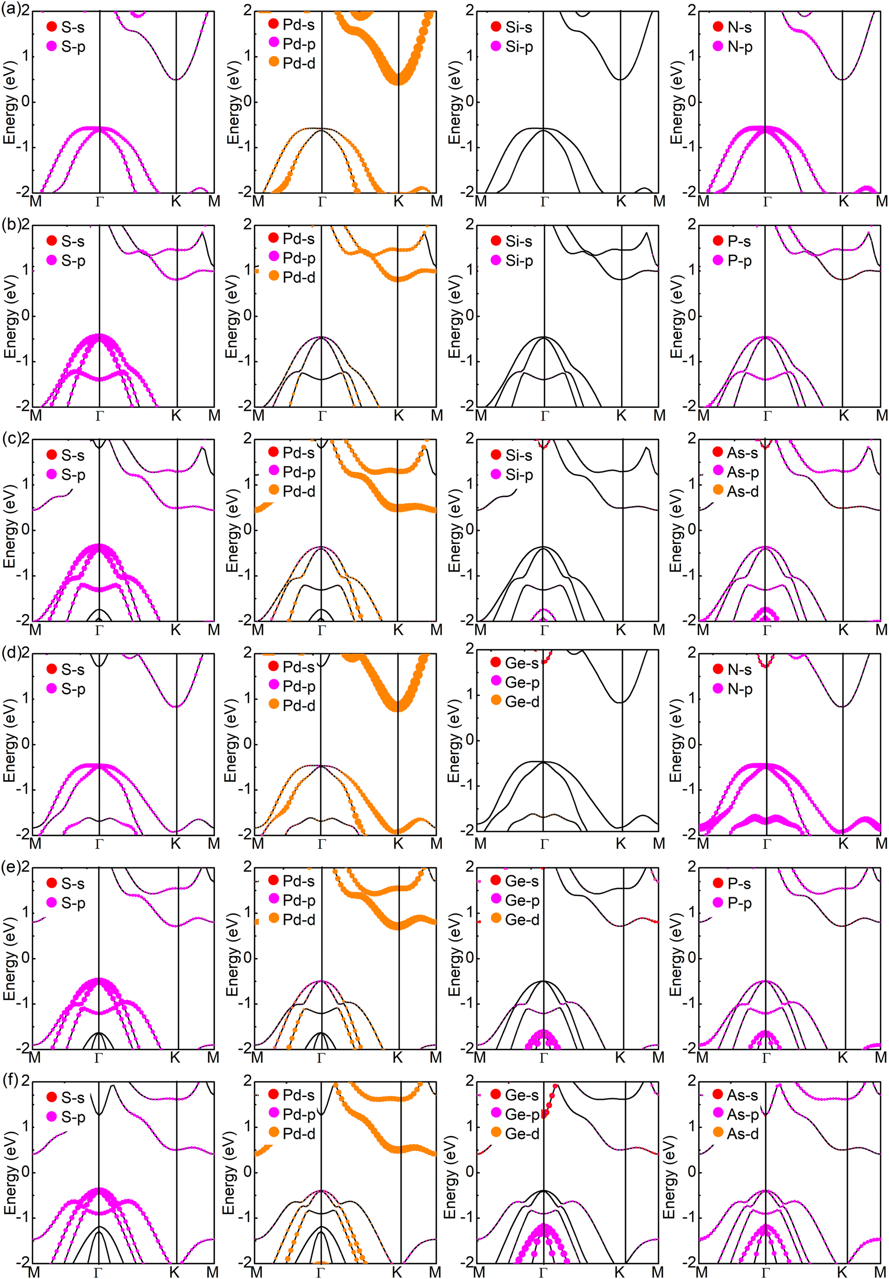 | ||
| Fig. 4 Projected band structure of 2D Janus (a) SPdSiN2, (b) SPdSiP2, (c) SPdSiAs2 (d) SPdGeN2, (e) SPdGeP2 and (f) SPdGeAs2 monolayers at equilibrium. | ||
3.3. Optical and photocatalytic properties of 2D SPdAZ2 (A = Si, Ge; Z = N, P, As) monolayers
To address environmental pollution, developing clean and renewable energy sources is an effective strategy. Solar energy and water are currently considered two of the most abundant resources on the earth. Therefore, photocatalytic water splitting by the sun to obtain hydrogen has attracted widespread attention.71–74 For excellent photocatalytic water decomposition catalysts, several important characteristics need to be met. First, the band gap of the material should fall within the range of 1.23–3 eV. This range ensures effective sunlight absorption, providing the necessary energy for water splitting. Secondly, for a semiconductor photocatalyst to effectively facilitate the photocatalytic decomposition of water, the band edge arrangement must align with the reduction and oxidation potentials involved in water splitting. When photons are absorbed by semiconductor catalysts, they generate electron–hole pairs. Electrons and holes can generate hydrogen and oxygen based on two reactions: 2H+ + 2e− → H2 and 2H2O + 4h+ → 4H+ + O2.75 To achieve the hydrogen evolution reaction (HER) of photocatalytic decomposition of water, the CBM of the photocatalyst relative to the vacuum level is required to be higher than the reduction potential . To complete the oxygen evolution reaction (OER) of photocatalytic decomposition of water, it is required that the VBM of the photocatalyst relative to the vacuum level is lower than the oxidation potential
  .76,77 The redox potential of photocatalytic water splitting depends on the pH value, and its formula is as follows:78,79
Thirdly, strong light absorption is crucial for generating electron–hole pairs when the photocatalyst absorbs sunlight. According to the photocatalytic mechanism for water decomposition, the 2D Janus structure can effectively separate electrons and hole carriers by adjusting the intrinsic dipole. In the case of 2D Janus materials, we clearly found that the Janus structure does not have the same vacuum energy level, leading to a difference in the vacuum energy level ΔΦ. J. L. Yang et al. proposed that the reduction and oxidation potentials of one side of water decomposition decrease as a result of ΔΦ. Consequently, they introduced a novel approach for designing efficient photocatalytic materials responsive to near-infrared light. In the conventional photocatalytic mechanism, it is typically required that the band gap value is equal to or greater than 1.23 eV to facilitate the overall water splitting reaction. However, for Janus materials, the criterion for the band gap value in photocatalytic materials has been redefined as Eg > 1.23 − ΔΦ eV, where ΔΦ > 0 and Eg > 0. This redefinition suggests that materials with band gap values less than 1.23 eV also hold great potential for use in water splitting under near-infrared light. Furthermore, for a larger ΔΦ, i.e., ΔΦ > 1.23 eV, there is no restriction on the band gap value.23 Therefore, we proceeded to calculate the band edge positions of SPdAZ2 monolayers using the HSE06 hybrid functional approach as proposed by Toroker et al.80 The results are presented in Fig. S4 (ESI†). It is evident from Fig. S4 (ESI†) that despite the redefinition of band gap values for photocatalytic materials within the 2D Janus structure, the SPdSiN2, SPdGeN2, and SPdGeAs2 monolayers remain incapable of simultaneously meeting the redox requirements of water. They can only exceed the oxidation necessary for the water oxidation reaction.

Furthermore, it is important to highlight that the pH level of water plays a crucial role in determining the reduction and oxidation potentials. The standard potentials of  and
and  can be determined using the equations mentioned earlier. As illustrated in Fig. 5a, the band edge alignment of the 2D Janus SPdAZ2 (A = Si, Ge; Z = N, P, As) structures was calculated at various pH values using the HSE06 functional. It was observed that by adjusting the pH value from 0 to 7, the CBM of the SPdAZ2 monolayers consistently falls below the reduction potential required for hydrogen production, indicating that the hydrogen-evolving capability of the SPdAZ2 monolayers is eliminated. Consequently, the capacity of SPdAZ2 monolayers to photocatalytically decompose water is advantageous under acidic conditions (pH = 0).
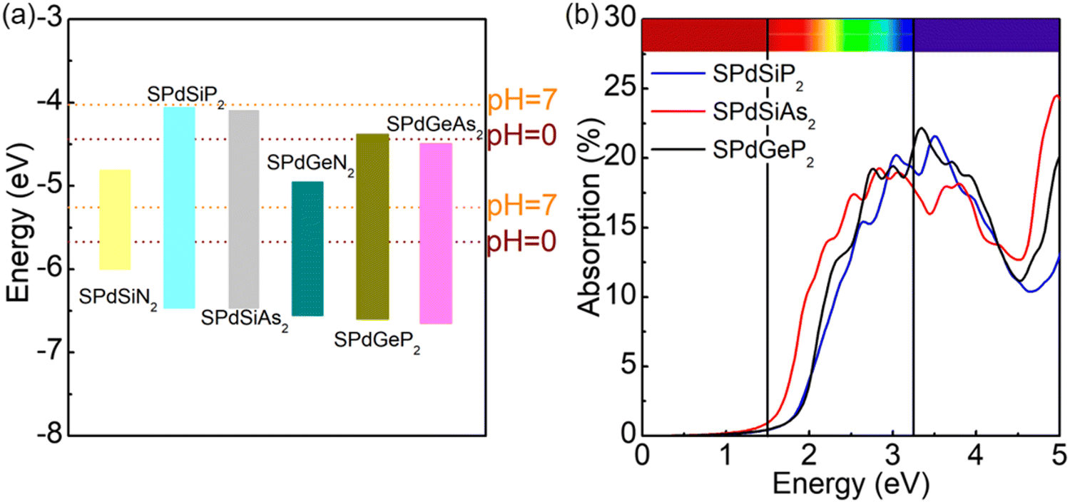 | ||
| Fig. 5 (a) Band alignments at pH = 0 and pH = 7 using the HSE06 functional of Janus SPdAZ2 (A = Si, Ge; Z = N, P, As) monolayers. (b) The optical absorption of SPdAZ2 (A = Si, Ge; Z = N, P, As) monolayers. | ||
Being an outstanding photocatalytic material, it can maximize sunlight absorption, thereby achieving higher utilization efficiency. Consequently, we calculated the optical absorption spectrum of 2D Janus SPdAZ2 (A = Si, Ge; Z = N, P, As) structures using the HSE06 functional, and the absorption coefficient is determined using the following formula:81
The solar-to-hydrogen (STH) efficiency is also a standard for evaluating the performance of photocatalysts. As mentioned above, high light absorption abilities of these monolayers are beneficial for high STH efficiencies, which can be calculated according to previous studies.33,83,84 Before calculating the STH efficiencies, one first needs to obtain the overpotentials χ(H2) and χ(O2) of the HER and OER, respectively, which characterize the redox capabilities of carriers. χ(H2) and χ(O2) could be obtained by calculating the difference between the CBM and H+/H2, and VBM and H2O/O2 potential, respectively, whose values are given in Table 4. All the overpotentials are positive and larger than 0.2 eV except χ(H2) of SPdSiN2, SPdGeN2 and SPdGeAs2, indicating that photogenerated carriers can obtain sufficient energy from these Janus monolayers to proceed with the HER and OER. These four kinds of energy conversion efficiencies of SPdAZ2 can be obtained from Table 3. It is found that ηabs of all Janus monolayers can reach up to 72% and ηcu values are higher than 56% except for SPdSiN2, SPdGeN2 and SPdGeAs2 monolayers. ηSTH values higher than 10% of all SPdAZ2 monolayers are obtained through the combination of high ηabs and ηcu.  values are still above 10% after considering intrinsic dipole, which makes these monolayers economically feasible. Due to the smallest band gap of the SPdSiAs2 monolayer, it has the highest STH efficiency, up to 36.65%. Such a high theoretical STH efficiency of SPdAZ2 monolayers is higher than that of 2D γ-GeSSe (28.78%),83 Pd4S3Se3 (30.1%)84 and In2Te3 (32.1%)33 monolayers. Therefore, the SPdAZ2 monolayers exhibit great potential for achieving economic production of hydrogen from photocatalytic water splitting.
 of SPdAZ2 (A = Si, Ge; Z = N, P, As)
| Phase | χ(H2) | χ(O2) | η abs (%) | η cu (%) | η STH (%) |
|
|---|---|---|---|---|---|---|
| SPdSiN2 | −0.373 | 1.562 | 81.95 | 36.60 | 30.00 | 28.44 |
| SPdSiP2 | 0.380 | 2.033 | 72.71 | 62.66 | 45.56 | 31.93 |
| SPdSiAs2 | 0.347 | 2.028 | 93.78 | 76.04 | 71.31 | 36.65 |
| SPdGeN2 | −0.513 | 2.121 | 71.36 | 25.14 | 17.94 | 16.10 |
| SPdGeP2 | 0.068 | 2.152 | 75.96 | 56.86 | 43.19 | 31.13 |
| SPdGeAs2 | −0.045 | 2.211 | 91.40 | 62.15 | 56.81 | 32.39 |

3.4. Transport of free photoexcited carriers
Once electron–hole pairs are separated, it is crucial for the free, light-excited carriers to efficiently migrate to chemically active sites for water decomposition. The rapid transport of photo-generated carriers to these active sites is of paramount importance. Consequently, we have employed the deformation potential theory (DP) to calculate the carrier mobility of these six 2D Janus structures.85 To investigate the carrier mobility in the x and y directions, we used a rectangular crystal cell, as shown in Fig. S5 (ESI†).The effective masses of carriers, which depend on the band structure of the region around the band-edges, were determined by fitting a parabolic function to the CBM (electrons) and VBM (holes) using the following equation:
The in-plane stiffness (C2D) can be calculated by simulating the total energy (E) change of the applied strain (ε) facilitated by the 2D materials using the equation C2D = [∂2E/∂ε2]/S0, where S0 is the surface area of the optimized supercell. The linear relationship between the band edge for the VBM and CBM and the strain exertion (ε) along the x and y direction, respectively, was fitted to estimate the deformation potential (DP) constant (E1).
According to the DP theory, the following expression can be used to determine the carrier mobility of 2D materials,85
|
|
|
C 2Dx | C 2Dy | |E1x| | |E1y| | μ x | μ y | ||
|---|---|---|---|---|---|---|---|---|---|
| SPdSiN2 | Electron | 0.584 | 0.584 | 178.91 | 178.93 | 0.576 | 0.577 | 22![[thin space (1/6-em)]](https://www.rsc.org/images/entities/char_2009.gif) 565.6 565.6 |
22523.2 |
| Hole | 2.258 | 2.258 | 178.91 | 178.93 | 6.019 | 6.045 | 13.849 | 13.733 | |
| SPdSiP2 | Electron | 1.227 | 1.227 | 113.15 | 113.16 | 0.598 | 0.700 | 3005.26 | 2193.49 |
| Hole | 3.066 | 3.066 | 113.15 | 113.16 | 6.930 | 6.940 | 3.584 | 3.574 | |
| SPdSiAs2 | Electron | 1.592 | 1.592 | 95.03 | 95.02 | 1.388 | 1.372 | 278.303 | 284.813 |
| Hole | 2.146 | 2.146 | 95.03 | 95.02 | 6.460 | 6.430 | 7.071 | 7.136 | |
| SPdGeN2 | Electron | 0.299 | 0.299 | 158.48 | 158.48 | 1.212 | 0.898 | 17256.6 |
31408.1 |
| Hole | 1.251 | 1.251 | 158.48 | 158.48 | 4.561 | 4.409 | 69.60 | 74.50 | |
| SPdGeP2 | Electron | 1.121 | 1.121 | 107.20 | 107.19 | 0.310 | 0.303 | 12694.1 |
13286.5 |
| Hole | 2.078 | 2.078 | 107.20 | 107.19 | 6.470 | 6.462 | 8.481 | 8.501 | |
| SPdGeAs2 | Electron | 0.960 | 0.960 | 86.508 | 86.516 | 1.606 | 1.582 | 520.75 | 536.72 |
| Hole | 1.336 | 1.336 | 86.508 | 86.516 | 6.266 | 6.216 | 17.644 | 17.931 |
Table 5 reveals a notable disparity in carrier mobility between electrons and holes in the same direction. In the case of SPdAZ2 monolayers, the difference in the same direction should be at least an order of magnitude. As a result of these substantial variations in carrier mobility, the separation of photo-generated carriers is further intensified within the Janus SPdAZ2 (A = Si, Ge; Z = N, P, As) monolayers.
3.5. Biaxial strain effect on 2D Janus SPdAZ2 (A = Si, Ge; Z = N, P, As) monolayers
Previous research has extensively demonstrated that the electronic properties of 2D structures can be readily adjusted under external conditions. In particular, applying strain to a structure can induce changes in its electronic properties,86–89 as can the application of an external electric field.89,90 These alterations in the band structure can, in turn, impact the photocatalytic and optical properties of the structure, given the direct correlation between optical characteristics and band gap.86–88 Consequently, we conducted an investigation into how biaxial strain and an external electric field affect the electronic, photocatalytic, and optical properties of 2D Janus SPdAZ2 (A = Si, Ge; Z = N, P, As) monolayers. Our initial focus was on examining the influence of biaxial strain on structural properties. Initially, we determined the maximum elastic threshold that a single-layered SPdAZ2 (A = Si, Ge; Z = N, P, As) could withstand through stress–strain curves, as depicted in Fig. S6a–j (ESI†). The data from Fig. S6a–j (ESI†) reveal that SPdAZ2 (A = Si, Ge; Z = N, P, As) monolayers can endure pressures of at least 6.1 N m−1 under tensile strain, featuring a minimum ideal strain of +8% and a maximum ideal strain of +27%. This mechanical strength surpasses that of the other renowned 2D materials like molybdenum disulfide (20%),91 highlighting the exceptional mechanical resilience of 2D Janus SPdAZ2 (A = Si, Ge; Z = N, P, As) monolayers. This quality makes them suitable for applications in electromechanical devices and strain sensors. Consequently, when investigating the electronic properties, we explored strain ranges of −8% to +8% for the SPdGeAs2 monolayer and −10% to +10% for the other five structures.Subsequently, we initiated the calculation of the phonon spectra for SPdAZ2 (A = Si, Ge; Z = N, P, As) monolayers across the examined biaxial strain range, as depicted in Fig. S7 (ESI†). Our calculations revealed that except for SPdSiN2 and SPdGeN2, which exhibit imaginary frequencies when subjected to compressive strain reaching −10%, the other structures can stably exist within the range of biaxial strain considered. Next, we delved into the alterations in the band gap of SPdAZ2 (A = Si, Ge; Z = N, P, As) structures under the influence of biaxial strain, as illustrated in Fig. 6a. As shown in Fig. 6a, we note that under compressive strain conditions, the single layers of SPdAZ2 (A = Si, Ge; Z = N, P, As) can transition from semiconductor to metallic properties. Conversely, under tensile strain, the semiconductor properties remain unaltered.
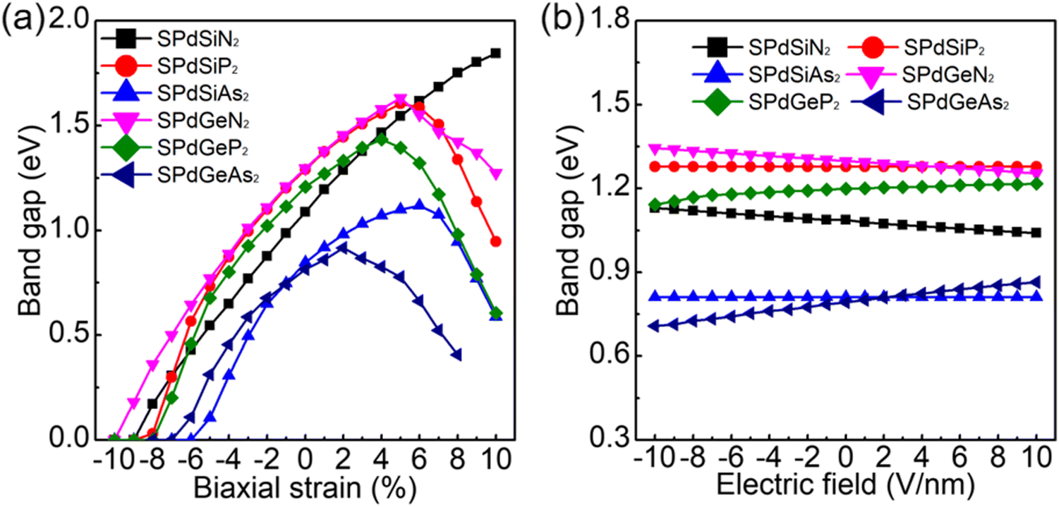 | ||
| Fig. 6 Band gap under (a) biaxial strain and (b) external electric field of 2D Janus SPdAZ2 (A = Si, Ge; Z = N, P, As) monolayers using the HSE method. | ||
The changes in band gaps directly impact the photocatalytic and optical properties of the structure. Consequently, we proceeded to investigate the effect of biaxial strain on the photocatalytic and optical properties of SPdAZ2 (A = Si, Ge; Z = N, P, As) monolayers. In this analysis, we examined the variations in SPdAZ2 (A = Si, Ge; Z = N, P, As) monolayers within the strain range of −5% to +5% at pH = 0. The band edge alignment of SPdAZ2 (A = Si, Ge; Z = N, P, As) monolayers is presented in Fig. 7. Our findings from Fig. 7 indicate that the single layers of SPdSiN2 and SPdGeN2 do not alter their ability to photocatalytically decompose water across the range of strains considered. In contrast, both SPdSiP2 and SPdSiAs2 monolayers can simultaneously facilitate water oxidation and reduction processes within the strain range of −5% to +5%. The SPdGeP2 monolayer demonstrates both water oxidation and reduction capabilities within the compressive strain range of −5% to 0%. However, under tensile strain, specifically when the tensile strain reaches +3%, its CBM falls below the reduction potential of water. As a result, the reduction ability disappears, and only water oxidation can occur. Remarkably, the SPdGeAs2 monolayer exhibits a unique behavior. When subjected to compressive strain at −2%, it gains the ability to simultaneously oxidize and reduce water, enabling complete water hydrolysis reactions. These results emphasize that under acidic conditions (pH = 0), the magnitude and type of biaxial strain can profoundly influence the photocatalytic performance of SPdAZ2 (A = Si, Ge; Z = N, P, As) structures.
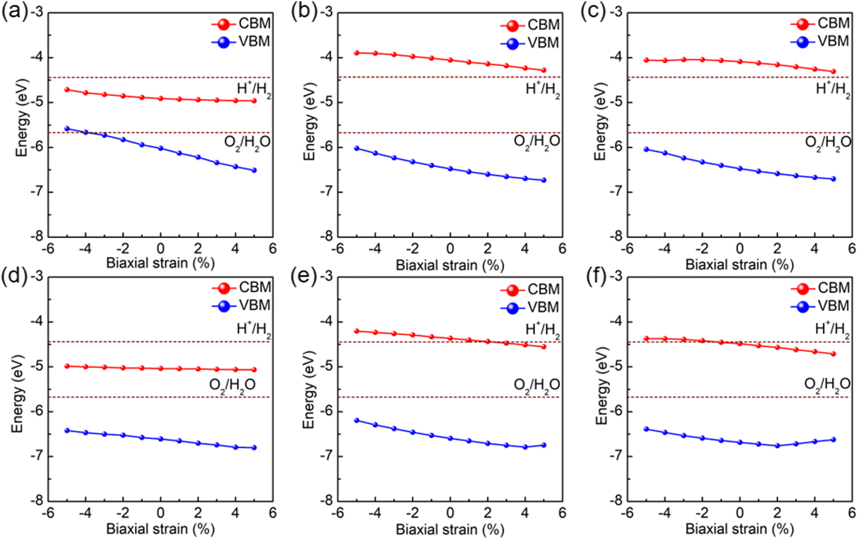 | ||
| Fig. 7 Band alignments of Janus (a) SPdSiN2, (b) SPdSiP2, (c) SPdSiAs2 (d) SPdGeN2, (e) SPdGeP2 and (f) SPdGeAs2 monolayers under biaxial strain. | ||
Finally, we explored the light absorption performance of the photocatalytic structures in the single layers of SPdAZ2 (A = Si, Ge; Z = N, P, As) under biaxial strain, as illustrated in Fig. 8. It is evident from Fig. 8 that as the strain increases gradually, the absorption of visible light also increases progressively. Additionally, a red shift phenomenon is observed with increasing strain, indicating the tunability of the structure's performance through strain manipulation.
 | ||
| Fig. 8 The light absorption of Janus (a) SPdSiP2, (b) SPdSiAs2, (c) SPdGeP2 and (d) SPdGeAs2 monolayers under biaxial strain. | ||
3.6. External electric field on 2D Janus SPdAZ2 (A = Si, Ge; Z = N, P, As) monolayers
In addition to the modulation of electronic properties through strain, it is worth noting that applying an external electric field to the structure can also achieve this effect, both theoretically and experimentally. We applied an external electric field perpendicular to the 2D Janus surface, with electric field strengths ranging from −10 V nm−1 to +10 V nm−1 (Fig. S8, ESI†). The electric field is considered positive when oriented along the positive z-axis and negative when oriented in the opposite direction of the z-axis. In experimental settings, pulsed AC electric field techniques92 have been utilized to generate electric fields, achieving strengths of approximately 7 V nm−1 through methods such as pulsed AC fields93 or surface doping techniques.94 Therefore, selecting an applied electric field ranging from −10 V nm−1 to +10 V nm−1 is a reasonable choice. Using the HSE06 functional, the band gap exhibits variations with the electric field, as depicted in Fig. 6b. The figure illustrates that the energy band structures of SPdAZ2 monolayers are all affected to some extent. In contrast to strain engineering, the influence of an external electric field on the band structure of the Janus SPdAZ2 monolayer is quite weak. This characteristic is also observed in some other Janus structures.87,89,95 Since changes in the band gap directly impact the photocatalytic and optical properties of the structure, our subsequent exploration focused on these aspects, with results presented in Fig. S9 and S10 (ESI†). As shown in Fig. S9 (ESI†), it becomes evident that SPdSiN2 and SPdGeN2 still lack the ability of water reduction, whereas SPdSiP2, SPdSiAs2, and SPdGeP2 monolayers continue to exhibit both water oxidation and reduction capabilities. Notably, the SPdGeAs2 monolayer exhibits both water oxidation and reduction abilities when subjected to a positive electric field of +2 V nm−1, which is an interesting discovery. Given the relatively significant impact of the applied electric field on SPdGeP2 and SPdGeAs2 monolayers, we also conducted calculations to assess the light absorption properties of these two structures, as shown in Fig. S10 (ESI†). As the applied electric field has a relatively minor effect on these two structures, the variations in their light absorption capacity are also relatively small, aligning closely with their photocatalytic performance. In conclusion, the properties of these structures can be more or less modulated by applying both strain and an external electric field.4. Conclusion
In summary, we utilized first principles calculations based on density-functional theory to investigate various aspects of 2D Janus SPdAZ2 (A = Si, Ge; Z = N, P, As) monolayers, including their structure, stability, electronic properties at equilibrium, photocatalytic and optical properties, and carrier mobility. Additionally, we explored how these properties change under the influence of biaxial strain and an externally applied electric field. Our findings indicate that SPdAZ2 (A = Si, Ge; Z = N, P, As) monolayers exhibit robust dynamical, thermal and mechanical stability. Using the HSE06 functional, all SPdAZ2 (A = Si, Ge; Z = N, P, As) monolayers display indirect band gap semiconductor properties. Furthermore, owing to the asymmetry inherent in the SPdAZ2 (A = Si, Ge; Z = N, P, As) structure, there exists an inherent built-in electric field within the material. This intrinsic electric field plays a pivotal role in efficiently separating and transporting photo-generated electrons and holes. In the equilibrium state, we observed that only SPdSiP2, SPdSiAs2 and SPdGeP2 monolayers can simultaneously engage in the photocatalytic decomposition of water. Notably, the photocatalytic decomposition of water is more favorable for SPdAZ2 (A = Si, Ge; Z = N, P, As) monolayers under acidic conditions (pH = 0) in comparison to neutral conditions (pH = 7). Through the calculation of carrier mobility in SPdAZ2 (A = Si, Ge; Z = N, P, As) monolayers, we have identified that structures capable of photocatalytic water decomposition exhibit significantly different electron and hole carrier mobilities, emphasizing the effectiveness of Janus structures in facilitating the efficient separation and transfer of photo-generated electrons and holes. Lastly, we have investigated the impact of biaxial strain and an applied electric field on SPdAZ2 (A = Si, Ge; Z = N, P, As) monolayers. Remarkably, under compressive strain and a positive electric field, the SPdGeAs2 monolayer can aid in both water oxidation and reduction, thereby enhancing the photocatalytic water decomposition process. Our findings present a promising avenue for the development of 2D Janus SPdAZ2 (A = Si, Ge; Z = N, P, As) materials as efficient photocatalysts for water splitting.Conflicts of interest
The authors declare that they have no known competing financial interests or personal relationships that could have appeared to influence the work reported in this paper.Acknowledgements
This work was supported by the National Natural Science Foundation of China (Grant No. 12164050 and 12264022), the Major Science and Technology Project of Precious Metal Materials Genetic Engineering in Yunnan Province (Grant No. 2019ZE001-1, 202002AB080001-6, 2018IC058), the Program for Yunling Scholars in Yunnan Province, the Program for Donglu Scholars in Yunnan University, and the Project of the Science Research foundation of the Department of Education in Yunnan Province.References
- A. Fujishima and K. Honda, Nature, 1972, 238, 37–38 CrossRef CAS PubMed.
- J. Schneider and D. W. Bahnemann, J. Phys. Chem. Lett., 2013, 4, 3479–3483 CrossRef CAS.
- G. Zhang, Z.-A. Lan, L. Lin, S. Lin and X. Wang, Chem. Sci., 2016, 7, 3062–3066 RSC.
- C. Luo, X. Ren, Z. Dai, Y. Zhang, X. Qi and C. Pan, ACS Appl. Mater. Inter., 2017, 9, 23265–23286 CrossRef CAS PubMed.
- X. Shi, Z. Lou, P. Zhang, M. Fujitsuka and T. Majima, ACS Appl. Mater. Inter., 2016, 8, 31738–31745 CrossRef CAS PubMed.
- S. Cho, C. Ahn, J. Park and S. Jeon, Nanoscale, 2018, 10, 9747–9751 RSC.
- S. Lee, Y. Lee, D. H. Kim and J. H. Moon, ACS Appl. Mater. Inter., 2013, 5, 12526–12532 CrossRef CAS PubMed.
- T. Yanagida, Y. Sakata and H. Imamura, Chem. Lett., 2004, 33, 726–727 CrossRef CAS.
- J. Sato, N. Saito, Y. Yamada, K. Maeda, T. Takata, J. N. Kondo, M. Hara, H. Kobayashi, K. Domen and Y. Inoue, J. Am. Chem. Soc., 2005, 127, 4150–4151 CrossRef CAS PubMed.
- A. Ishikawa, T. Takata, J. N. Kondo, M. Hara, H. Kobayashi and K. Domen, J. Am. Chem. Soc., 2002, 124, 13547–13553 CrossRef CAS PubMed.
- A. Kudo and Y. Miseki, Chem. Soc. Rev., 2009, 38, 253–278 RSC.
- J. Schneider, M. Matsuoka, M. Takeuchi, J. Zhang, Y. Horiuchi, M. Anpo and D. W. Bahnemann, Chem. Rev., 2014, 114, 9919–9986 CrossRef CAS PubMed.
- T.-Y. Park, Y.-S. Choi, S.-M. Kim, G.-Y. Jung, S.-J. Park, B.-J. Kwon and Y.-H. Cho, Appl. Phys. Lett., 2011, 98, 251111 CrossRef.
- M. Cardona, Phys. Rev., 1965, 140, A651–A655 CrossRef.
- S. Cao and J. Yu, J. Phys. Chem. Lett., 2014, 5, 2101–2107 CrossRef CAS PubMed.
- B. Hinnemann, P. G. Moses, J. Bonde, K. P. Jørgensen, J. H. Nielsen, S. Horch, I. Chorkendorff and J. K. Nørskov, J. Am. Chem. Soc., 2005, 127, 5308–5309 CrossRef CAS PubMed.
- M. Qiao, J. Liu, Y. Wang, Y. Li and Z. Chen, J. Am. Chem. Soc., 2018, 140, 12256–12262 CrossRef CAS PubMed.
- L. Ju, J. Shang, X. Tang and L. Kou, J. Am. Chem. Soc., 2020, 142, 1492–1500 CrossRef CAS PubMed.
- L. Ju, M. Bie, J. Shang, X. Tang and L. Kou, Journal of Physics: Materials, 2020, 3, 022004 CAS.
- J. Fernández-Catalá, A. A. Kistanov, Y. Bai, H. Singh and W. Cao, npj 2D Mater. Appl., 2023, 7, 48 CrossRef.
- W.-J. Ong, L.-L. Tan, Y. H. Ng, S.-T. Yong and S.-P. Chai, Chem. Rev., 2016, 116, 7159–7329 CrossRef CAS PubMed.
- P. Zhao, Y. Ma, X. Lv, M. Li, B. Huang and Y. Dai, Nano Energy, 2018, 51, 533–538 CrossRef CAS.
- X. Li, Z. Li and J. Yang, Phys. Rev. Lett., 2014, 112, 018301 CrossRef PubMed.
- A.-Y. Lu, H. Zhu, J. Xiao, C.-P. Chuu, Y. Han, M.-H. Chiu, C.-C. Cheng, C.-W. Yang, K.-H. Wei, Y. Yang, Y. Wang, D. Sokaras, D. Nordlund, P. Yang, D. A. Muller, M.-Y. Chou, X. Zhang and L.-J. Li, Nat. Nanotechnol., 2017, 12, 744–749 CrossRef CAS PubMed.
- J. Zhang, S. Jia, I. Kholmanov, L. Dong, D. Er, W. Chen, H. Guo, Z. Jin, V. B. Shenoy, L. Shi and J. Lou, ACS Nano, 2017, 11, 8192–8198 CrossRef CAS PubMed.
- X. Ma, X. Wu, H. Wang and Y. Wang, J. Mater. Chem. A, 2018, 6, 2295–2301 RSC.
- L. Ju, M. Bie, X. Tang, J. Shang and L. Kou, ACS Appl. Mater. Inter., 2020, 12, 29335–29343 CAS.
- G. Almeida, S. Dogan, G. Bertoni, C. Giannini, R. Gaspari, S. Perissinotto, R. Krahne, S. Ghosh and L. Manna, J. Am. Chem. Soc., 2017, 139, 3005–3011 CrossRef CAS PubMed.
- C. Cui, W.-J. Hu, X. Yan, C. Addiego, W. Gao, Y. Wang, Z. Wang, L. Li, Y. Cheng, P. Li, X. Zhang, H. N. Alshareef, T. Wu, W. Zhu, X. Pan and L.-J. Li, Nano Lett., 2018, 18, 1253–1258 CrossRef CAS PubMed.
- R. B. Jacobs-Gedrim, M. Shanmugam, N. Jain, C. A. Durcan, M. T. Murphy, T. M. Murray, R. J. Matyi, R. L. Moore, II and B. Yu, ACS Nano, 2014, 8, 514–521 CrossRef CAS PubMed.
- J. Zhou, Q. Zeng, D. Lv, L. Sun, L. Niu, W. Fu, F. Liu, Z. Shen, C. Jin and Z. Liu, Nano Lett., 2015, 15, 6400–6405 CrossRef CAS PubMed.
- F. Xue, J. Zhang, W. Hu, W.-T. Hsu, A. Han, S.-F. Leung, J.-K. Huang, Y. Wan, S. Liu, J. Zhang, J.-H. He, W.-H. Chang, Z. L. Wang, X. Zhang and L.-J. Li, ACS Nano, 2018, 12, 4976–4983 CrossRef CAS PubMed.
- C.-F. Fu, J. Sun, Q. Luo, X. Li, W. Hu and J. Yang, Nano Lett., 2018, 18, 6312–6317 CrossRef CAS PubMed.
- P. Wang, H. Liu, Y. Zong, H. Wen, J.-B. Xia and H.-B. Wu, ACS Appl. Mater. Inter., 2021, 13, 34178–34187 CrossRef CAS PubMed.
- J. Qiu, H. Li, X. Chen, B. Zhu, H. Guo, F. Zhang, Z. Ding, L. Lang, J. Yu and J. Bao, J. Appl. Phys., 2021, 129, 125109 CrossRef CAS.
- J. Qiu, F. Zhang, H. Li, X. Chen, B. Zhu, H. Guo, Z. Ding, J. Bao and J. Yu, IEEE Electron Device Lett., 2021, 42, 561–564 CAS.
- Y.-L. Hong, Z. Liu, L. Wang, T. Zhou, W. Ma, C. Xu, S. Feng, L. Chen, M.-L. Chen, D.-M. Sun, X.-Q. Chen, H.-M. Cheng and W. Ren, Science, 2020, 369, 670–674 CrossRef CAS PubMed.
- Y. Yu, J. Zhou, Z. Guo and Z. Sun, ACS Appl. Mater. Inter., 2021, 13, 28090–28097 CrossRef CAS PubMed.
- C.-c Jian, X. Ma, J. Zhang and X. Yong, J. Phys. Chem. C, 2021, 125, 15185–15193 CrossRef CAS.
- B. Mortazavi, B. Javvaji, F. Shojaei, T. Rabczuk, A. V. Shapeev and X. Zhuang, Nano Energy, 2021, 82, 105716 CrossRef CAS.
- J. Chen and Q. Tang, Chem. – Eur. J., 2021, 27, 9925–9933 CrossRef CAS PubMed.
- A. Yadav, J. Kangsabanik, N. Singh and A. Alam, J. Phys. Chem. Lett., 2021, 12, 10120–10127 CrossRef CAS PubMed.
- Y. Liu, Y. Ji and Y. Li, J. Phys. Chem. Lett., 2021, 12, 9149–9154 CrossRef CAS PubMed.
- H. Zhao, G. Yang, Y. Liu, X. Yang, Y. Gu, C. Wei, Z. Xie, Q. Zhang, B. Bian, X. Zhang, X. Huo and N. Lu, ACS Appl. Electron. Mater., 2021, 3, 5086–5094 CrossRef CAS.
- R. T. Sibatov, R. M. Meftakhutdinov and A. I. Kochaev, Appl. Surf. Sci., 2022, 585, 152465 CrossRef CAS.
- Z. Gao, X. He, W. Li, Y. He and K. Xiong, Dalton Trans., 2023, 52, 8322–8331 RSC.
- Z. Gao, X. He, W. Li, Y. He and K. Xiong, Appl. Surf. Sci., 2023, 158146 CrossRef CAS.
- S. T. Nguyen, P. V. Cuong, N. Q. Cuong and C. V. Nguyen, Dalton Trans., 2022, 51, 14338–14344 RSC.
- G. Yuan, X. Ma, J. Liao, T. Xie, Q. Xie and Z. Yuan, ACS Appl. Nano Mater., 2023, 6, 1956–1964 CrossRef CAS.
- T. V. Vu, H. V. Phuc, C. V. Nguyen, V. T. T. Vi, A. I. Kartamyshev and N. N. Hieu, Phys. Chem. Chem. Phys., 2022, 24, 16512–16521 RSC.
- A. Rezavand and N. Ghobadi, Mater. Sci. Semicond. Process., 2022, 152, 107061 CrossRef CAS.
- Z.-Q. Tian, B. Ren and D.-Y. Wu, J. Phys. Chem. B, 2002, 106, 9463–9483 CrossRef CAS.
- C. R. Henry, Surf. Sci. Rep., 1998, 31, 231–325 CrossRef CAS.
- S. Cheong, J. D. Watt and R. D. Tilley, Nanoscale, 2010, 2, 2045–2053 RSC.
- A. D. Oyedele, S. Yang, L. Liang, A. A. Puretzky, K. Wang, J. Zhang, P. Yu, P. R. Pudasaini, A. W. Ghosh, Z. Liu, C. M. Rouleau, B. G. Sumpter, M. F. Chisholm, W. Zhou, P. D. Rack, D. B. Geohegan and K. Xiao, J. Am. Chem. Soc., 2017, 139, 14090–14097 CrossRef CAS PubMed.
- L.-H. Zeng, D. Wu, S.-H. Lin, C. Xie, H.-Y. Yuan, W. Lu, S. P. Lau, Y. Chai, L.-B. Luo, Z.-J. Li and Y. H. Tsang, Adv. Funct. Mater., 2019, 29, 1806878 CrossRef.
- K. Zhao, X. Li, S. Wang and Q. Wang, Phys. Chem. Chem. Phys., 2019, 21, 246–251 RSC.
- S. Qian, X. Sheng, X. Xu, Y. Wu, N. Lu, Z. Qin, J. Wang, C. Zhang, E. Feng, W. Huang and Y. Zhou, J. Mater. Chem. C, 2019, 7, 3569–3575 RSC.
- G. Kresse and J. Furthmüller, Phys. Rev. B: Condens. Matter Mater. Phys., 1996, 54, 11169–11186 CrossRef CAS PubMed.
- P. E. Blöchl, Phys. Rev. B: Condens. Matter Mater. Phys., 1994, 50, 17953–17979 CrossRef PubMed.
- J. P. Perdew, K. Burke and M. Ernzerhof, Phys. Rev. Lett., 1996, 77, 3865–3868 CrossRef CAS PubMed.
- J. Heyd and G. E. Scuseria, J. Chem. Phys., 2004, 121, 1187–1192 CrossRef CAS PubMed.
- A. Togo, F. Oba and I. Tanaka, Phys. Rev. B: Condens. Matter Mater. Phys., 2008, 78, 134106 CrossRef.
- S. Baroni, S. D. Gironcoli, A. D. Corso and P. Giannozzi, Rev. Mod. Phys., 2001, 73, 515–562 CrossRef CAS.
- C. Qi, C. Yan, Q. Li, T. Yang, S. Qiu and J. Cai, J. Mater. Chem. C, 2023, 11, 3262–3274 RSC.
- N. N. Hieu, H. V. Phuc, A. I. Kartamyshev and T. V. Vu, Phys. Rev. B, 2022, 105, 075402 CrossRef CAS.
- Z.-j Wu, E.-j Zhao, H.-p Xiang, X.-f Hao, X.-j Liu and J. Meng, Phys. Rev. B: Condens. Matter Mater. Phys., 2007, 76, 054115 CrossRef.
- A. Castellanos-Gomez, M. Poot, G. A. Steele, H. S. J. van der Zant, N. Agraït and G. Rubio-Bollinger, Adv. Mater., 2012, 24, 772–775 CrossRef CAS PubMed.
- L. Wang, A. Kutana, X. Zou and B. I. Yakobson, Nanoscale, 2015, 7, 9746–9751 RSC.
- H. Xiao, J. Tahir-Kheli and W. A. Goddard, J. Phys. Chem. Lett., 2011, 2, 212–217 CrossRef CAS.
- Y. Cui, L. Peng, L. Sun, Q. Qian and Y. Huang, J. Mater. Chem. A, 2018, 6, 22768–22777 RSC.
- R. da Silva, R. Barbosa, R. R. Mançano, N. Durães, R. B. Pontes, R. H. Miwa, A. Fazzio and J. E. Padilha, ACS Appl. Nano Mater., 2019, 2, 890–897 CrossRef CAS.
- Y.-M. Zhao, P. Ren, X. Ma, J. P. Lewis, Q.-B. Yan and G. Su, J. Phys. Chem. C, 2021, 125, 11939–11949 CrossRef CAS.
- A. K. Singh, K. Mathew, H. L. Zhuang and R. G. Hennig, J. Phys. Chem. Lett., 2015, 6, 1087–1098 CrossRef CAS PubMed.
- B. Mortazavi, B. Javvaji, F. Shojaei, T. Rabczuk, A. V. Shapeev and X. Zhuang, arXiv:2012.14706, 2020 DOI:10.48550/arXiv.2012.14706.
- Y. Li, Y.-L. Li, B. Sa and R. Ahuja, Catal. Sci. Technol., 2017, 7, 545–559 RSC.
- H. L. Zhuang and R. G. Hennig, JOM, 2014, 66, 366–374 CrossRef.
- V. Chakrapani, J. C. Angus, A. B. Anderson, S. D. Wolter, B. R. Stoner and G. U. Sumanasekera, Science, 2007, 318, 1424–1430 CrossRef CAS PubMed.
- H. L. Zhuang and R. G. Hennig, Chem. Mater., 2013, 25, 3232–3238 CrossRef CAS.
- M. C. Toroker, D. K. Kanan, N. Alidoust, L. Y. Isseroff, P. Liao and E. A. Carter, Phys. Chem. Chem. Phys., 2011, 13, 16644–16654 RSC.
- X. Huang, T. R. Paudel, S. Dong and E. Y. Tsymbal, Phys. Rev. B: Condens. Matter Mater. Phys., 2015, 92, 125201 CrossRef.
- M. Y. Liu, Y. He, X. Li and K. Xiong, Phys. Chem. Chem. Phys., 2023, 25, 7278–7288 RSC.
- V. V. Thanh, D. V. Truong and N. T. Hung, ACS Appl. Energy Mater., 2023, 6, 910–919 CrossRef CAS.
- Y. Luo, M. Sun, J. Yu and U. Schwingenschlögl, Chem. Mater., 2021, 33, 4128–4134 CrossRef CAS.
- J. Bardeen and W. Shockley, Phys. Rev., 1950, 80, 72–80 CrossRef CAS.
- T. V. Vu, V. T. T. Vi, C. V. Nguyen, H. V. Phuc and N. N. Hieu, J. Phys. D: Appl. Phys., 2020, 53, 455302 CrossRef CAS.
- T. V. Vu, V. T. T. Vi, H. V. Phuc, C. V. Nguyen, N. A. Poklonski, C. A. Duque, D. P. Rai, B. D. Hoi and N. N. Hieu, J. Phys.: Condens. Matter, 2021, 33, 225503 CrossRef CAS PubMed.
- H. Liu, Z. Huang, C. He, Y. Wu, L. Xue, C. Tang, X. Qi and J. Zhong, J. Appl. Phys., 2018, 125, 082516 CrossRef.
- T. V. Vu, C. V. Nguyen, H. V. Phuc, A. A. Lavrentyev, O. Y. Khyzhun, N. V. Hieu, M. M. Obeid, D. P. Rai, H. D. Tong and N. N. Hieu, Phys. Rev. B, 2021, 103, 085422 CrossRef CAS.
- L. Debbichi, O. Eriksson and S. Lebègue, J. Phys. Chem. Lett., 2015, 6, 3098–3103 CrossRef CAS PubMed.
- T. Li, Phys. Rev. B: Condens. Matter Mater. Phys., 2012, 85, 235407 CrossRef.
- C. Vicario, B. Monoszlai and C. P. Hauri, Phys. Rev. Lett., 2018, 121, 259901 CrossRef CAS.
- C. Vicario, B. Monoszlai and C. P. Hauri, Phys. Rev. Lett., 2014, 112, 213901 CrossRef.
- J. Kim, S. S. Baik, S. H. Ryu, Y. Sohn, S. Park, B.-G. Park, J. Denlinger, Y. Yi, H. J. Choi and K. S. Kim, Science, 2015, 349, 723–726 CrossRef CAS PubMed.
- T. V. Vu, H. D. Tong, D. P. Tran, N. T. T. Binh, C. V. Nguyen, H. V. Phuc, H. M. Do and N. N. Hieu, RSC Adv., 2019, 9, 41058–41065 RSC.
Footnote |
| † Electronic supplementary information (ESI) available. See DOI: https://doi.org/10.1039/d3cp04936a |
| This journal is © the Owner Societies 2024 |