Experimental and computational DFT, drift-diffusion studies of cobalt-based hybrid perovskite crystals as absorbers in perovskite solar cells†
Received
26th September 2023
, Accepted 28th December 2023
First published on 2nd January 2024
Abstract
The optimised designs of dimethyl ammonium cobalt formate-based perovskite crystals [(CH3)2NH2]Co(HCOO)3 were experimentally synthesized and computationally utilized as absorbers for perovskite solar cells (PSCs). Crystals were grown using solvothermal synthesis. Additive materials (Fe, Ni) are responsible for the growth and suppression of crystals in the micrometre range. Temperature and pressure were altered to obtain optimum growth conditions. Grown crystals were characterized by spectroscopy (XRD, FT-IR, UV-Vis) and optical microscopy. Combined density functional theory (DFT) and drift-diffusion modelling frameworks were simulated. These simulators were used to examine various perovskite absorbers for solar-cell configurations. Field calculations were used to examine the structural stability, band structure, and electronic contribution of the constituent elements in [(CH3)2NH2]Co1−nMn(HCOO)3 (M = Fe, Ni and n = 0, 0.1) as absorber material. Conventional TiO2 and spiro-OMeTAD were used as the electron-transport layer and hole-transport layer, respectively, and Pt was used as a back contact. Comprehensive analysis of the effects of several parameters (layer thickness, series and shunt resistances, temperature, generation-recombination rates, current–voltage density, quantum efficiency) was carried out using simulation. Our proposed strategy may pave the way for further design of new absorber materials for PSCs.
1 Introduction
Lead-based perovskite solar cells have record efficiencies exceeding 25%. However, lead toxicity has raised concerns about their safety and environmental impact. Lead ions permanently contaminate soil and water supplies, which significantly affects the life of people, animals, and plants.1–6 To ensure that the environment around humans is safe and pollution-free, some non- or low-toxic metal ions must be created to replace lead as perovskite absorbers.7–12 As a result, there is a growing interest in lead-free perovskite solar cells. Perovskites have a general formula of ABX3, where A is an inorganic/organic cation (DMA, ammonium, guanidium, and imidazolium are used), B is a transition ion (e.g., Co, Fe, Ni, Zn), and X is usually a halide or oxide.13 However, researchers focused recently on the family of formate perovskites in which the formate anion HCOO− occupies the linker site. The ABX3 type of MOF has a porous structure formed by CO and HCOO−; the porous cavities are occupied by DMA ions. These hybrid perovskite MOF crystals are used for applications such as photovoltaic systems, drug delivery, LEDs, multiferroic systems, and switchable electronics.4,14–16 Multiferroicity is the property of exhibiting simultaneous magnetic and electric ordering. This offers the probability of magnetoelectric coupling, which is electric control of magnetization (or) magnetic control of dielectric polarization. Scholars have reported on the crystal structure, dielectric characteristics, and heat capacity of [(CH3)2NH2] Zn (HCOO)3. This chemical exhibits crystallisation in the R3C space group during the paraelectric phase. The cobalt ion has an octahedral coordination, surrounded by six oxygen atoms originating from six formate ions.17,18 These formate ions serve as interconnecting units, resulting in the formation of a three-dimensional framework. Dimethyl ammonium cobalt formate (DMACF) is a promising lead-free perovskite material with good optical and electronic properties. The methyl ammonium (MA) group in MAPbI3 is a promising material for photovoltaic applications because the MA cation has a small size and a relatively low polarizability. These features allow it to fit snugly into the perovskite lattice, which stabilizes the structure and reduces defects. In addition, the MA cation has a dipole moment, which contributes to the macroscopic polarization of the perovskite material. This polarization is important for efficient charge transport and light absorption. However, the issue with the material is its stability in normal ambient conditions. Using a methyl group with a metal formate ion in DMACF as an absorber in perovskite increases the stability; it is a perovskite-like metal formate (PLMF) structure that can promote the crystallization of perovskite films. The DMACF {[(CH3)2NH2]Co(HCOO)3} has a bandgap of 2.1 eV. This is a wider bandgap than that of traditional perovskite materials, such as methylammonium lead iodide (MAPbI3), which has a bandgap of 1.55 eV. A wider bandgap allows the material to absorb more sunlight, which can lead to higher power-conversion efficiency in solar cells. DMACF is also more stable than traditional perovskites. Traditional perovskites are prone to degradation under the actions of moisture and heat. DMACF is more stable, which makes it more suitable for use in commercial solar cells. In this work, the effects of Fe and Ni doping on the properties of DMACF crystals were investigated. Fe and Ni are transition metals that form perovskites. They also have a positive effect on the growth and properties of DMACF crystals. The addition of Fe has been shown to increase the crystal size and improve crystallinity because Fe can act as a template for the growth of DMACF crystals. Fe and Ni can also be used to substitute DMACF, which can further improve its properties. Doping can change the electrical conductivity, bandgap, and other properties of the material. In recent years, a significant amount of research has been conducted to enhance the efficiency of lead-free perovskite solar cells (PSCs).7,8,19,20 It is essential to use density functional theory (DFT) and simulation methods for these devices to understand the correlation between the material properties and performance of cells. The present study focused primarily on modelling and optimising device characteristics to understand the elements that impact the efficiency of PSCs. Solar cell capacitance simulator (SCAPS) 1D was used to assess and investigate the impact of several variables on the performance of a device. These properties included absorber thickness, working temperature, density of states, series resistance, and defect density. Drift-diffusion modelling can be utilised for this purpose.21–24 Material properties such as band structure, Eigen states, and the electron-density profile can be analysed by Device Studio software with a “nanodcal” package. Addition of Fe and Ni to DMACF can improve the bandgap of the material (an essential factor for solar-cell efficiency). It has been found that addition of Fe and Ni can increase the carrier concentration of a material,16,25 which can also improve the efficiency of the solar cell. Studies have suggested that: (i) DMACF with Fe and Ni doping is a promising lead-free perovskite material for solar-cell applications; (ii) DMACF with Fe and Ni substitution is a promising lead-free perovskite material for solar-cell applications. Further studies are needed to optimize the substitution levels and to investigate the long-term stability of these lead-free perovskite absorber materials.
2 Materials and methods
2.1 Experimental approach
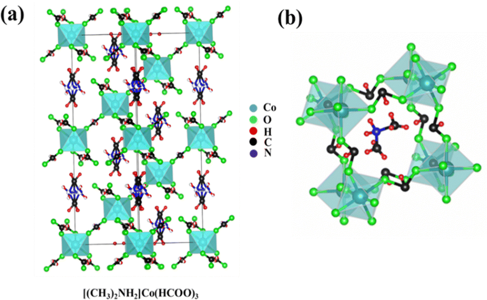
The crystallographic image of DMACF hydrate is shown in Fig. 1a. The unit cell of the three-dimensional (3D) network of crystals is shown in Fig. 1b, where A is an organic cation DMA, B is a transition ion (e.g., Co), and X is usually a halide or oxide. The single crystals of [(CH3)2NH2] Cox·M1−x(HCOO)3 (M = Fe, Ni and x = 0.1) were grown using a solvothermal solution. Briefly, 40 mL of DMF and 40 mL of DI water were added to a beaker. The mixture was stirred with a magnetic stirrer. Then, 5 mM of metal chlorides (Co, Co0.9Fe0.1, Co0.9Ni0.1) were added and stirred for 30 min at 500–550 rpm. Upon completion of stirring, the mixture was transferred to a Teflon™-lined autoclave and kept in a hot air oven at 140 °C. After 72 h, the autoclave was allowed to cool down to room temperature. The supernatant was transferred to a beaker. Crystals were left for 7 days at room temperature. Grown crystals were filtered and washed thrice with ethanol and dried at room temperature.26,27 These steps are shown schematically in Fig. 2.
 |
| | Fig. 1 (a) Crystal of DMACF hydrate perovskite (schematic). (b) Unit cell of a crystal of DMACF hydrate perovskite. | |
 |
| | Fig. 2 Steps for growing hybrid perovskite crystals. | |
The method used for hydrothermal development of crystals has a high degree of similarity to crystal formation from an aqueous solution under ambient conditions.28 The prescribed volume of solution was introduced to an autoclave at a certain pressure (P) and temperature (T), following thermodynamic principles. Solute molecules were transported from the hot zone to the cold zone by convection, facilitated by the difference in temperature (ΔT). The rate of crystal growth at the diaphragm opening and the choice of solvent were determined by thermodynamic factors: P, T, and ΔT.29
2.2 Computational approach
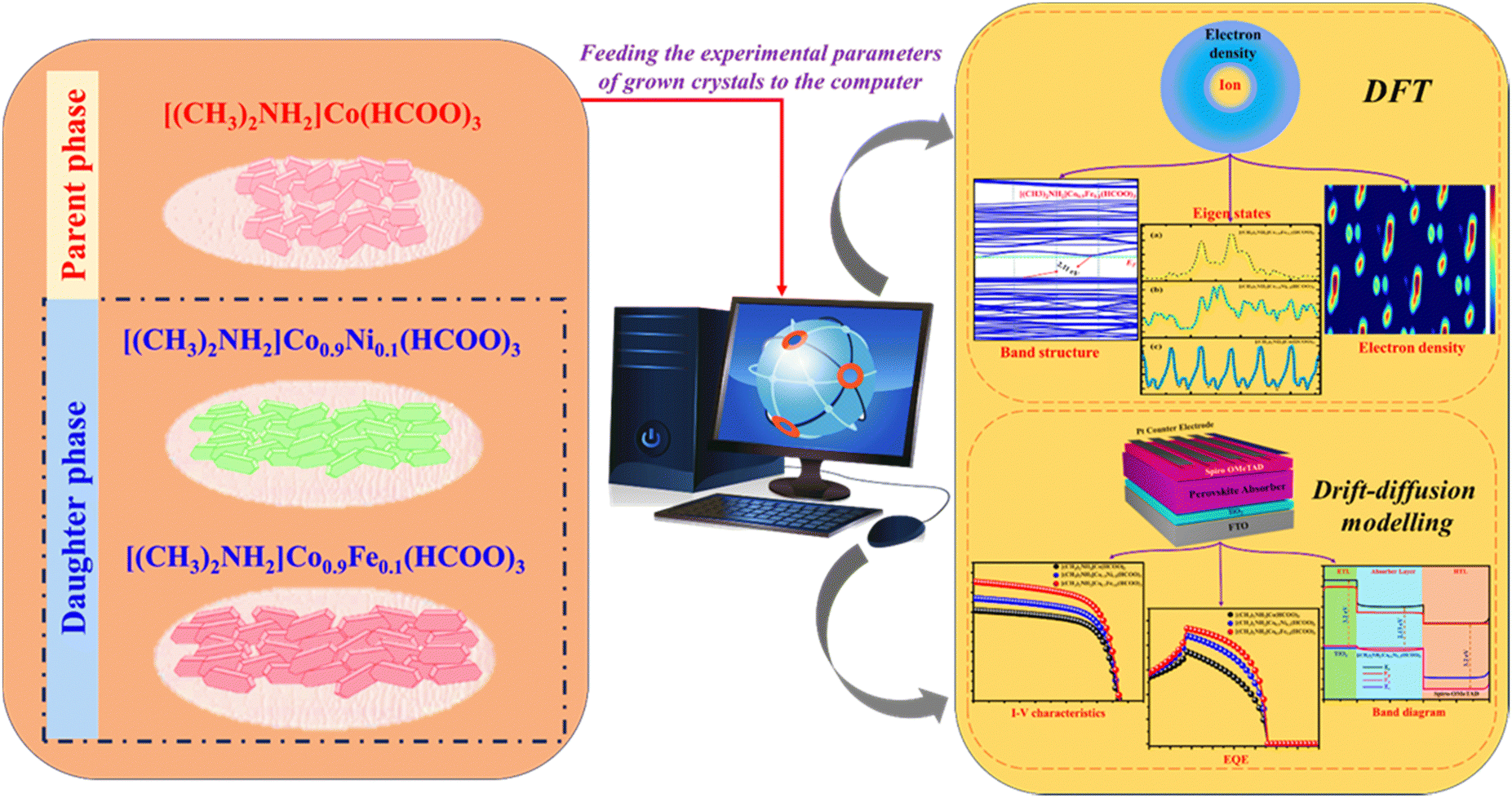
Crystals were grown using solvothermal synthesis (Table 1). Grown crystals were characterized using optical microscopy, X-ray diffraction (XRD), Raman spectroscopy, UV absorption, and differential scanning calorimetry (DSC). Experimentally obtained factors were fed as inputs for computational modelling and simulation. Material properties were analyzed by DFT. Device properties were modelled and analyzed by drift-diffusion studies. The workflow of the computational method is given in Fig. 3.
Table 1 Routes of crystal growth and properties of crystals
| Materials |
Method |
Chemicals used |
Crystal type |
Average length & width (μm) |
| [(CH3)2NH2]Co(HCOO)3 |
Synthesis: solvothermal solution route; crystallization: slow evaporation |
CoCl2·6H2O, DMF, DI water |
Rhombohedral |
600, 300 |
| [(CH3)2NH2]Co0.9Fe0.1(HCOO)3 |
Synthesis: solvothermal solution route; crystallization: slow evaporation |
CoCl2·6H2O, FeCl2·6H2O DMF, DI water |
Rhombohedral |
800, 400 |
| [(CH3)2NH2]Co0.9Ni0.1(HCOO)3 |
Synthesis: solvothermal solution route; crystallization: slow evaporation |
CoCl2·6H2O, NiCl2·6H2O DMF, DI water |
Rhombohedral |
350, 180 |
 |
| | Fig. 3 Computational approach (schematic). | |
2.2.1 DFT studies.
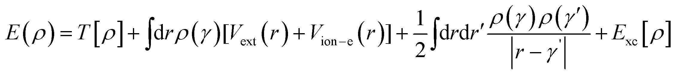
We undertook first-principle calculations exploiting nanodcal software engaged in DFT. In “nanodcal”, a self-consistent field theory calculates Hamiltonian and electronic structures. At equilibrium, this SCF theory is precisely DFT. DFT in “nanodcal” uses a linear combination of atomic orbital (LCAO) basis sets to expand all the physical operators. The foundational principles of DFT were first formulated by Hohenberg and Kohn30 and developed further by Kohn and Sham.31 These theorems assert that the energy of the lowest energy state of a system may be represented exclusively as a functional of the electronic density of the ground state.| |  | (1) |
where T[ρ] is the Kohn–sham kinetic energy, ρ(γ) is the total electron density, Vion–e(r), which is the interaction potential between valence electrons and ion cores (and these are defined by the pseudopotential), Exc is the exchange–correlation energy,  is the Coulomb interaction, and Vext(r) is any external potential (e.g., applied external bias potential). Use of the pseudo-potential plane-wave (PP-PW) total energy computation was employed to determine the ground-state structure of [(CH3)2NH2]Co(HCOO)3, [(CH3)2NH2]Co0.9Fe0.1(HCOO)3 and [(CH3)2NH2]Co0.9Ni0.1(HCOO)3 systems. The generalised gradient approximation (GGA) and Perdew–Burke–Ernzerhof functional were used to implement the exchange–correlation potential. A larger k-point grid size (8 × 8 × 8) was used to observe the pattern of electronic charge density.32–34 Utilisation of the Broyden–Fletcher–Goldfarb–Shanno algorithm was crucial for conducting structural optimisation and accurately determining the lattice constants, as well as the internal atomic coordinates of [(CH3)2NH2]Co(HCOO)3, [(CH3)2NH2]Co0.9Fe0.1(HCOO)3, and [(CH3)2NH2]Co0.9Ni0.1(HCOO)3.
Considering the above-mentioned characteristics, the band structure, eigenstates, and electron-density profile were computed for the optimised design.
2.2.2 Drift-diffusion studies.
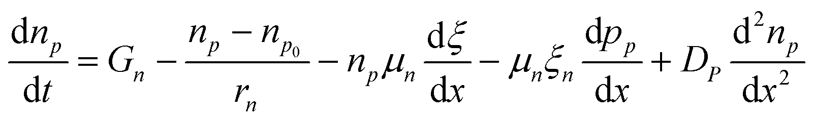
SCAPS 1D was used to simulate the selected structures. This numerical simulation programme was created by the Department of Electronics and Information Systems of University of Ghent (Belgium).35 The simulation in this software is based on Poisson's equation, and hole and electron continuity eqn (2)–(4). All simulations were carried out at a spectrum illumination of AM 1.5 with power density of 1000 W m−2 from the front side.| | 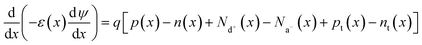 | (2) |
| |  | (3) |
| |  | (4) |
D denotes the diffusion coefficient, E is the electrostatic potential, and G is the generation rate and permittivity. p, n, pt, and ntv denote free holes, free electrons, trapped holes, and trapped electrons, respectively. Na− and Nd+ are abbreviations for ionised acceptor doping and donor concentrations, respectively.35
3 Results and discussion
3.1 Morphological structural analysis
Grown crystals were observed using an optical microscope. The size of the DMACF crystal increased by addition of Fe and decreased by addition of Ni because of the different ionic radii of Fe and Ni. The ionic radius of Fe is larger than the ionic radius of Ni, so Fe can fit readily into the crystal lattice, which results in a larger crystal size. The thermodynamics of different crystal sizes can affect the properties of the crystal. For example, a larger crystal size of the Fe-doped crystal may result in a higher carrier concentration, which can improve the efficiency of the solar cell. The ionic radius of Fe is ∼0.08 Å larger than the ionic radius of Ni. This slight difference in ionic radius can have a significant effect on crystal size. Different crystal sizes can also affect the optical properties of the crystal. For example, the larger crystal size of the Fe-doped crystal may result in a higher absorption coefficient, which can improve the efficiency of the solar cell. In summary, Fe-doped and Ni-doped crystal sizes can significantly affect the properties of a crystal by impacting the carrier concentration, optical properties, and other crystal properties.
Data from powder XRD revealed that the crystals of [(CH3)2NH2]Co(HCOO)3 were rhombohedral. The morphology of crystals are given in Fig. 4. All peaks could be indexed to the space group R![[3 with combining macron]](https://www.rsc.org/images/entities/char_0033_0304.gif) c, indicating the phase purity of the sample. Lattice parameters increased linearly with the substitution of Fe and decreased by substituting Ni and Fe. Significant peaks were observed in the spectrum at 14.77, 20.23, 21.64, 26.30, 29.79 34.31, 39.11, and 44.10, with hkl values of (012), (104), (110), (113), (024), (122), (125), and (220), respectively, according to the ICDD (01-075-7839) database (Fig. 5a). In the parent phase (i.e. [(CH3)2NH2]Co(HCOO)3), the cell parameters have been reported to be a = 8.2062Å, c = 22.296 Å, and the volume of the crystal is ∼1300.29 Å3. The significant peak at 14.77 shifted slightly to the left by substituting Ni. The lattice parameters of a crystal are the distances between the atoms in the crystal. The substitution of Fe and Ni in DMACF can change the lattice parameters of the crystal because Fe and Ni have different ionic radii than Co. Hence, they occupy different positions in the crystal lattice. A shift in the peak positions of the XRD pattern can indicate a change in crystal structure. The substitution of Fe and Ni for Co in DMACF could change the crystal structure of the material, which could cause peak positions to shift.
c, indicating the phase purity of the sample. Lattice parameters increased linearly with the substitution of Fe and decreased by substituting Ni and Fe. Significant peaks were observed in the spectrum at 14.77, 20.23, 21.64, 26.30, 29.79 34.31, 39.11, and 44.10, with hkl values of (012), (104), (110), (113), (024), (122), (125), and (220), respectively, according to the ICDD (01-075-7839) database (Fig. 5a). In the parent phase (i.e. [(CH3)2NH2]Co(HCOO)3), the cell parameters have been reported to be a = 8.2062Å, c = 22.296 Å, and the volume of the crystal is ∼1300.29 Å3. The significant peak at 14.77 shifted slightly to the left by substituting Ni. The lattice parameters of a crystal are the distances between the atoms in the crystal. The substitution of Fe and Ni in DMACF can change the lattice parameters of the crystal because Fe and Ni have different ionic radii than Co. Hence, they occupy different positions in the crystal lattice. A shift in the peak positions of the XRD pattern can indicate a change in crystal structure. The substitution of Fe and Ni for Co in DMACF could change the crystal structure of the material, which could cause peak positions to shift.
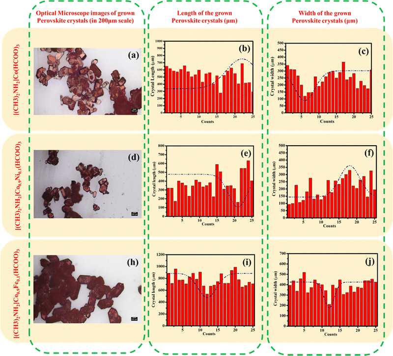 |
| | Fig. 4 Optical-microscope images of [(CH3)2NH2]Co(HCOO)3, [(CH3)2NH2]Co0.9Ni0.1(HCOO)3, and [(CH3)2NH2]Co0.9Fe0.1(HCOO)3. | |
 |
| | Fig. 5 (a) X-ray diffraction spectra. (b) FT-IR spectra. (c) UV-Vis spectra. (d) Tauc plot. (e) Raman spectra. (f) Differential scanning calorimetry of [(CH3)2NH2]Co(HCOO)3, [(CH3)2NH2]Co0.9Ni0.1(HCOO)3, and [(CH3)2NH2]Co0.9Fe0.1(HCOO)3. | |
3.2 Vibrational analysis
The FT-IR spectrum of the DMACF crystal was characterized by six peaks (Fig. 5b), two of which were significant in the range 1350 to 1570 cm−1. The minor peaks at 570 to 770 cm−1 and 2700 to 3300 cm−1 could be assigned. The significant peaks at 1350 to 1570 cm−1 were associated with the symmetric and asymmetric stretching vibrations of the formate ion. The minor peak at 570 to 770 cm−1 was associated with the bending vibrations of the formate ion. The minor rise at 2700 to 3300 cm−1 was associated with the stretching vibrations of the N–H bonds in the dimethyl ammonium cation. The presence of these peaks in the FT-IR spectrum of the DMACF crystal confirmed the presence of the formate ion and dimethyl ammonium cation in the crystal. The relative intensities of the peaks could be used to determine the relative concentrations of these two ions in the crystal. The different masses of Fe and Ni cause the vibrations of the formate ion to occur at slightly different frequencies. This is because the mass of the vibrating molecule affects the frequency. The different electronic structures of Fe and Ni also affect the frequency of the vibrations of the formate ion. The electronic structure of the molecule affects how the electrons absorb and emit energy. The different bonding interactions of Fe and Ni with the formate ion also affect the frequency of the vibrations because the bonding interactions affect the way the molecule vibrates. These new peaks were associated with the vibrations of Fe and Ni ions. The presence of these peaks could be used to study the bonding of Fe and Ni to the formate ion, and determine the structure of the crystal.
The Raman spectrum of DMACF and Fe, Ni DMACF had four active peaks (Fig. 5e). The prominent peak in the range 1360–1370 cm−1 was associated with the symmetric stretching vibration of the formate ion. The minor peaks at 480 to 610 cm−1 and 2950 cm−1 were associated with the bending vibration of the formate ion and stretching vibration of N–H bonds in the dimethyl ammonium cation. The peak at 1580 cm−1 was associated with the bending vibration of the dimethyl ammonium cation. Addition of Fe and Ni to the DMACF crystal did not change the Raman spectrum of the crystal significantly because the Fe and Ni ions did not have significant Raman-active modes. The presence of the four Raman operational modes confirmed the presence of the formate ion, dimethyl ammonium cation, and cobalt ion in the crystal. The relative intensities of the peaks could be used to determine the relative concentrations of these three ions in the crystal. The Raman spectrum of DMACF and Fe and Ni added to DMACF led to a good “fingerprint” of the crystal, and could be used to study the structure and composition of the crystal.
3.3 UV-Vis absorption
The inference from the UV-Vis absorption and Tauc plot for DMACF crystals as well as Fe and Ni added to DMACF crystals was that addition of Fe and Ni increased the bandgap of the crystals slightly (Fig. 5d). The absorbance of crystals at ∼500 nm corresponded to the absorption of photons with an energy of ∼2.1 eV (Fig. 5c). This was the bandgap of the crystals (i.e., the energy difference between valence and conduction bands). Addition of Fe and Ni to crystals increased the bandgap slightly, as evidenced by the slight shift of the absorbance peak to longer wavelengths. This was because Fe and Ni have higher atomic numbers than Co, so they have more electrons. These additional electrons fill-up the valence band, making it more difficult for electrons to be excited into the conduction band. The bandgap increase upon addition of Fe and Ni is a desirable property for solar-cell applications. This is because a wider bandgap means that the solar cell can absorb photons with higher energy, which results in higher efficiency. In addition to the increase in the bandgap, the addition of Fe and Ni may also have other effects on the properties of crystals.
3.4 Investigation of thermal properties
The DSC profile of DMACF as well as Fe and Ni added to DMACF is an excellent way to study the phase transitions of the crystal. The melting point of the crystal is affected by the molecular weight of the ions in the crystal. The decomposition temperature of the crystal is the temperature at which the crystal breaks down into its constituent ions. The decomposition temperature of the crystal is also affected by the molecular weight of the ions in the crystal. The DSC profile of DMACF as well as Fe and Ni added to DMACF showed two endothermic reactions at 186 and 300 °C, which revealed that the crystal underwent two phase transitions (Fig. 5f). The first endothermic reaction at 186 °C corresponded to melting of the crystal. The value of change in enthalpy (ΔH) was calculated to be 653.47 J g−1 for the parent phase, 620.50 J g−1 for Fe-substituted, and 692.04 J g−1 for Ni-substituted Co-based Formate crystals. The second endothermic reaction at 300 °C corresponded to decomposition of the crystal. Addition of Fe and Ni to the crystal shifted the peaks in the DSC profile slightly. The value of ΔH was 976.02 J g−1 for the parent phase, 809.33 J g−1 for Fe-substituted, and 982.02 J g−1 for Ni-substituted Co-based formate crystals. Fe and Ni ions have a different molecular weight than that of Co. The additional molecular weight affects the melting point and decomposition temperature of the crystal. Addition of Fe and Ni can also affect the crystal structure, which can cause the peaks to shift. The endothermic peak at 300 °C in the DSC profile of DMACF as well as Fe and Ni added to DMACF was split into two peaks. The decomposition of the crystal could occur through two mechanisms, decomposition of the (i) formate ion; (ii) dimethyl ammonium cation.
3.5 Eigenstate profile
The Eigenstate profile is used for molecular or periodic bulk systems. It gives eigen energies and corresponding wave functions as a vector of the coefficients of a set of atomic bases and as a real-space function for a group of specified states. Eigenstates are the solutions to the Schrödinger equation for a particular system. They represent the possible states that an electron can occupy in the system. The different profiles for Fe- and Ni-added crystals indicated that addition of Fe and Ni to crystal changed the energy levels of electrons. This is because Fe and Ni have different electronic structures than those of Co, so they interact with the electrons in the crystal differently, which can increase or decrease the bandgap. The Eigenstate profile of [(CH3)2NH2]Co(HCOO)3, [(CH3)2NH2]Co0.9Ni0.1(HCOO)3, and [(CH3)2NH2]Co0.9Fe0.1(HCOO)3 is given in Fig. 6, which revealed that addition of Fe and Ni to crystals changed the energy levels of electrons and bandgap of the system. The different profiles for Fe- and Ni-added crystals indicated that adding Fe and Ni to the crystal could change the optical properties and carrier concentration of the system.
 |
| | Fig. 6 Eigenstates profile of [(CH3)2NH2]Co(HCOO)3, [(CH3)2NH2]Co0.9Fe0.1(HCOO)3, and [(CH3)2NH2]Co0.9Ni0.1(HCOO)3 crystals on XY, YZ, and XZ plane. The value of X, Y, and Z coordinates is given in Å. | |
3.6 Calculation of the band structure
The slight change in the bandgap of DMACF crystals (parent phase) as well as Fe and Ni added to DMACF with k points of mesh (8 × 8 × 8) could be explained by quantum mechanical principles. The energy difference between the valence band and conduction band determines the bandgap of a material. The valence band is the band of energy levels filled with electrons. The conduction band is the band of empty energy levels. Addition of Fe and Ni to the crystal could change the energy levels of the electrons in the valence band and conduction band (Fig. 7a–c). The bandgap for the parent phase was calculated to be 2.15 eV and 2.13 eV for Ni-substituted and 2.11 eV for Fe-substituted Co-based formate crystals. This was because Fe and Ni have different electronic structures than Co, so they interact with the electrons in the crystal differently. The inference of our study was that addition of Fe and Ni to DMACF crystals could change the bandgap of crystals. This change in the bandgap could be used to improve the properties of the crystal for solar-cell applications. The band-structure profile indicated that addition of Fe and Ni to the crystal could change the energy levels of the electrons in the valence band and conduction band. This change in the energy levels of electrons can cause a slight change in the bandgap of crystals and hence could be used to improve the properties of the crystal for photovoltaic applications.
 |
| | Fig. 7 Band structure of [(CH3)2NH2]Co(HCOO)3, [(CH3)2NH2]Co0.9Ni0.1(HCOO)3, and [(CH3)2NH2]Co0.9Fe0.1(HCOO)3 crystals. | |
3.7 Electron-density profile
The electron-density profile is a plot of the electron density in a material as a function of position (Fig. 8). It can be used to understand the distribution of electrons in the material in coordinate space XY (Fig. 8c, f and j), YZ (Fig. 8a, d and h), and XZ (Fig. 8b, e and i) planes. The slight variation in the electron-density profile for Fe- and Ni-added phases than the parent phase indicated that adding Fe and Ni to the crystal changed the distribution of electrons in the crystal. This is because Fe and Ni have different electronic structures to that of Co, meaning they interact with the electrons in the crystal differently. The importance of the study is that it provides insights into the effect of Fe and Ni on the electronic structure of DMACF crystals. This information can be used to design new materials with improved properties for solar-cell applications. Thus, the electron-density profile suggested that the addition of Fe and Ni to the crystal changed the distribution of electrons in the crystal. This change in the distribution of electrons could affect the optical properties of the crystal, which could affect the efficiency of solar cells. In addition, the change in the electron-density profile could affect the carrier concentration of the crystal.
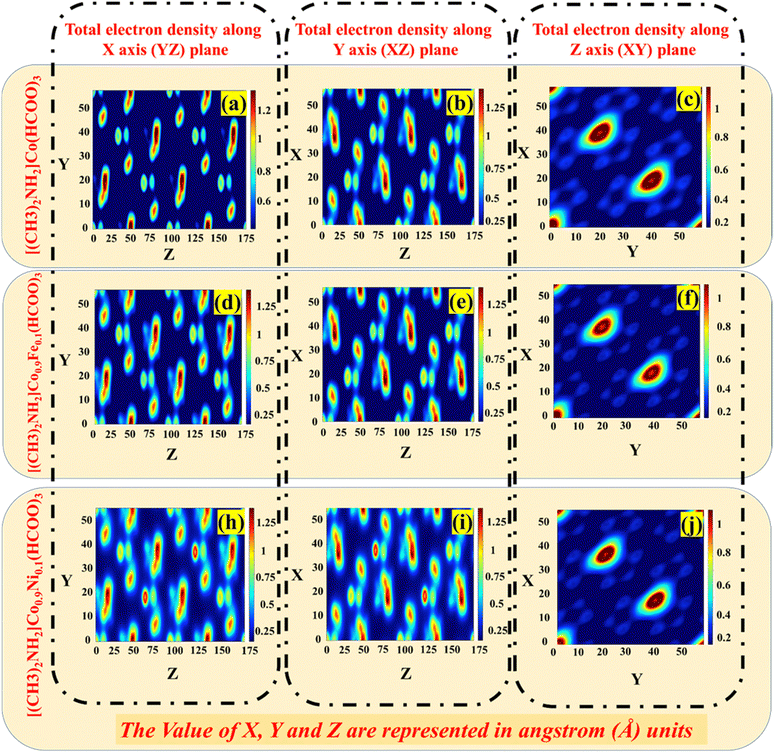 |
| | Fig. 8 Electron-density profile of [(CH3)2NH2]Co(HCOO)3, [(CH3)2NH2]Co0.9Ni0.1(HCOO)3, and [(CH3)2NH2]Co0.9Fe0.1(HCOO)3 crystals. | |
4 Device simulation
Three devices were simulated using drift-diffusion modelling by SCAPS. The parameters used to build the device are shown in Tables 2 and 3. The architecture of the simulated devices is shown in Fig. 9a–c.
Table 2 Parameters used for the simulation of PSCs based on [(CH3)2NH2]Co(HCOO)3, [(CH3)2NH2]Co0.9Ni0.1(HCOO)3, and [(CH3)2NH2]Co0.9Fe0.1(HCOO)3
| Parameters |
TiO2 |
[(CH3)2NH2]Co(HCOO)3 |
[(CH3)2NH2]Co0.9Ni0.1(HCOO)3 |
[(CH3)2NH2]Co0.9Fe0.1(HCOO)3 |
Spiro-OMeTAD |
| Thickness (nm) |
100 |
200-1100 |
200-1100 |
200-1100 |
100 |
| Bandgap (eV) |
3.2 |
2.15 |
2.13 |
2.11 |
3.2 |
| Electron affinity (eV) |
4 |
3.9 |
3.9 |
4 |
2.1 |
| Dielectric permittivity |
10 |
9 |
9 |
9 |
3 |
| CB effective density of states (cm−3) |
2.2 × 10¹⁸ |
1.8 × 10¹⁸ |
1.0 × 10¹⁹ |
1.0 × 10¹⁹ |
2.5 × 10¹⁸ |
| VB effective density of states (cm−3) |
1.9 × 10¹⁸ |
1.0 × 10¹⁹ |
1.0 × 10¹⁹ |
1.0 × 10¹⁹ |
1.8 × 10¹⁹ |
| Electron thermal velocity (cm s−1) |
1.0 × 10⁷ |
1.0 × 10⁷ |
1.0 × 10⁷ |
1.0 × 10⁷ |
1.0 × 10⁷ |
| Hole thermal Velocity (cm s−1) |
1.0 × 10⁷ |
1.0 × 10⁷ |
1.0 × 10⁷ |
1.0 × 10⁷ |
1.0 × 10⁷ |
| Electron mobility (cm2 V−1 s−1) |
2 |
0.5 |
0.5 |
0.5 |
2 × 10⁻⁴ |
| Hole mobility (cm2 V−1 s−1) |
1 |
0.5 |
0.5 |
0.5 |
2 × 10⁻⁴ |
| Donor density ND (cm−3) |
1 × 10¹⁸ |
0 |
0 |
0 |
0 |
| Acceptor density NA (cm−3) |
0 |
1 × 10¹⁶ |
1 × 10¹⁶ |
1 × 10¹⁶ |
1 × 10²⁰ |
Table 3 Parameters for front and back contacts
| Parameters |
Front contact |
Back contact |
| Metalwork function (eV) |
4.3 |
5.7 |
| Surface recombination velocity of electrons (cm s−1) |
1 × 10⁷ |
1 × 10⁵ |
| Surface recombination velocity of holes (cm s−1) |
5 × 10⁵ |
1 × 10⁷ |
 |
| | Fig. 9 A schematic of simulated device configurations by drift-diffusion modelling using (a) [(CH3)2NH2]Co(HCOO)3 as an absorber, (b) [(CH3)2NH2]Co0.9Ni0.1(HCOO)3 as an absorber, and (c) [(CH3)2NH2]Co0.9Fe0.1(HCOO)3 as an absorber in a perovskite solar cell. | |
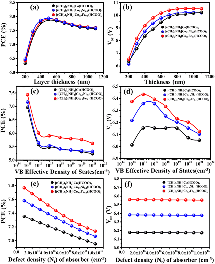
4.1 Effect of thickness of the light-absorber layer
PSC efficiency is strongly affected by the thickness of the light-absorber layer. The mathematical representation of the link between the solar spectrum and response of the device can be established by including the variable of the thickness of the photon-absorber layer. We used TiO2 as the electron-transport layer (ETL) material and Spiro-OMeTAD as the hole-transport layer (HTL) material to investigate the impact of variation of absorber-layer thickness. ([(CH3)2NH2]Co(HCOO)3, [(CH3)2NH2]Co0.9Ni0.1(HCOO)3, and [(CH3)2NH2]Co0.9Fe0.1(HCOO)3) from 200 nm to 1.1 μm were used. Fig. 10a and b depicts the relationship between thickness, efficiency, and open circuit potential (Voc). The expression for the open circuit voltage (Voc) of the device is:| |  | (5) |
where n is the diode ideality factor, kT/q is the thermal voltage, I0 is the dark-saturation current, and IL is the light-saturation current. In the case of [(CH3)2NH2]Co(HCOO)3, [(CH3)2NH2]Co0.9Ni0.1(HCOO)3, and [(CH3)2NH2]Co0.9Fe0.1(HCOO)3 absorbers, the PSC exhibited an upward trend as the thickness of the device rose within a range of 6.25% to 8% until reaching a wavelength of 550 nm. Subsequently, the PSC experienced a decline to 7.5% owing to an observed augmentation in the diffusion length of the device.36 The efficiency increased up to 550 nm because the absorber layer could absorb most of the incident sunlight at that thickness. However, if the absorber layer was thicker than 550 nm, it started to reflect more light back out of the cell, which reduced the efficiency. The open-circuit voltage (Voc) of [(CH3)2NH2]Co(HCOO)3, [(CH3)2NH2]Co0.9Ni0.1(HCOO)3, and [(CH3)2NH2]Co0.9Fe0.1(HCOO)3 absorbers exhibited a linearly rising trend if the thickness was varied. In this context, the photons traverse the depleted region by significant absorption within the absorber layer. Consequently, the generated electron–hole pair migrates towards the depleted zone instead of experiencing surface recombination throughout its lifespan.37 Simulation results indicated that selection of the absorber-layer thickness should be based on the diffusion length of charge carriers. An absorber layer of increased thickness within a wavelength range 200–550 nm could absorb more photons, resulting in enhanced efficiency at AM 1.5 G.38
 |
| | Fig. 10 Effect of absorber thickness on (a) PCE and (b) Voc while keeping the working temperature, series resistance, density of states, and defect density constant. Effect of valence-band density of states on (c) PCE and (d) Voc while keeping the working temperature, series resistance, thickness, and defect density constant. Effect of defect density on (e) PCE and (f) Voc while keeping the working temperature, series resistance, thickness, and density of states constant. | |
4.2 Effect of density of states (DOS) on device performance
An investigation was conducted to ascertain the impact of the DOS of DMACF compound. The chemical compounds [(CH3)2NH2]Co(HCOO)3, [(CH3)2NH2]Co0.9Ni0.1(HCOO)3, and [(CH3)2NH2]Co0.9Fe0.1(HCOO)3 are of interest in academic research. The DOS of absorber layers varied from 1015 to 1021 cm−3.39Fig. 10c and d illustrate the relationship between the efficiency of the device and Voc with respect to the DOS. A negative correlation between the efficiency and effective DOS in the perovskite absorber layer was observed.
4.3 Effect of defect density on device performance
An increased defect density at the interface of the absorber layer leads to hysteresis in the perovskite layer.40,41 In this simulation, the defect density was varied from 1.0 × 10¹⁵ to 1.0 × 10¹⁶![[thin space (1/6-em)]](https://www.rsc.org/images/entities/char_2009.gif) 42 while keeping the other parameters constant. Simulation results indicated a progressive decline in cell efficiency with increasing defect density (Fig. 10e and f). Likewise, Voc exhibited a comparable trend when the flaw density was augmented. The increase in trap states has a detrimental impact on the band structure of a material, leading to significant recombination inside the layer.38 The incorporation of Ni and Fe into the [(CH3)2NH2]Co(HCOO)3 perovskite material can lead to significant enhancement in the overall performance of cells.43 Moreover, the same outcome was observed with the rise in flaw density. The decline in PCE did not impact the Voc of the device.
42 while keeping the other parameters constant. Simulation results indicated a progressive decline in cell efficiency with increasing defect density (Fig. 10e and f). Likewise, Voc exhibited a comparable trend when the flaw density was augmented. The increase in trap states has a detrimental impact on the band structure of a material, leading to significant recombination inside the layer.38 The incorporation of Ni and Fe into the [(CH3)2NH2]Co(HCOO)3 perovskite material can lead to significant enhancement in the overall performance of cells.43 Moreover, the same outcome was observed with the rise in flaw density. The decline in PCE did not impact the Voc of the device.
4.4. Effect of temperature on device performance
With regard to PSCs, the operating temperature is a crucial parameter. Jsc and Voc are closely connected to their operating temperature. For most device simulations, an operating temperature of 300 K was used. The working temperature of the device was altered from 300 to 400 K under continuous irradiation of 1000 W m−2 to understand the influence of temperature on [(CH3)2NH2]Co(HCOO)3, [(CH3)2NH2]Co0.9Ni0.1(HCOO)3, and [(CH3)2NH2]Co0.9Fe0.1(HCOO)3. Fig. 11a and b depict the efficiency and Voc as a function of temperature. As the temperature increased, the device overall efficiency decreased dramatically. The reverse saturation current grows exponentially as the device temperature rises, thereby lowering Voc.44 Simulation findings suggested that the working temperature had a direct connection with the efficiency of MAPbI3 PSC. In [(CH3)2NH2]Co(HCOO)3, [(CH3)2NH2]Co0.9Ni0.1(HCOO)3, and [(CH3)2NH2]Co0.9Fe0.1(HCOO)3, the efficiency increased slightly (300 to 350 K) and then decreased (350 to 400 K). Voc had a consistent value across all three absorbers. The increase in temperature led to a reduction in the concentration of the electron mobility carrier of the device, resulting in a decrease in efficiency.45,46 The operational temperature influenced the efficiency and power production of the PSC significantly.
 |
| | Fig. 11 Effect of temperature on (a) PCE and (b) Voc while keeping the defect density, series resistance, thickness, and density of states constant. Effect of series resistance on (c) PCE and (d) Voc of the device while keeping the thickness, working temperature, density of states, and defect density constant. Optimized device performance: (e) JV and (f) EQE of [(CH3)2NH2]Co(HCOO)3, [(CH3)2NH2]Co0.9Fe0.1(HCOO)3, and [(CH3)2NH2]Co0.9Ni0.1(HCOO)3 perovskite solar cells. | |
4.5 Effect of series resistance on device performance
The series resistance has significant importance in the performance of the device. The fill factor and Jsc are directly affected by it.| | | Isc = I0(eVocq/nKT − 1) | (6) |
| |  | (7) |
The presence of series resistance mainly arises from the inherent resistance of metallic contacts in the device's upper and rear sections. In this study, the materials FTO and Pt were used as the contact materials for the device. The open circuit voltage (Voc) of the devices with absorbers remained constant while the series resistance was altered since no current was being pulled from the device cell.47 The impact of series resistance on the power conversion efficiency (PCE) is seen in Fig. 11c and d. It is noted that when the series resistance was incrementally raised from 1 to 10 Ω cm−2, there is a drop in the PCE. The simulation results have verified that the inclusion of nickel (Ni) and iron (Fe) into the original compound, namely [(CH3)2NH2]Co(HCOO)3, has resulted in a 0.1 enhancement in efficiency.
4.6 Optimized device performance
The final device was simulated using optimized parameters: active layer thickness, operating temperature, valence-band DOS, defect density, and series resistance. Fig. 11e depicts the performance of [(CH3)2NH2]Co(HCOO)3, [(CH3)2NH2]Co0.9Fe0.1(HCOO)3, and [(CH3)2NH2]Co0.9Ni0.1(HCOO)3 PSCs, and the efficiencies of the devices were calculated to be 6.44%, 7.20%, and 7.98%, respectively. The Ni- and Fe-substituted device generated Jsc values of 11.40 mA cm−2 and 13.07 mA cm−2, which were 1.22- and 2.89-times greater than the Jsc of the parent phase. Voc of the devices was 0.938 V for the parent phase, 0.943 V for the Ni-substituted cell, and 0.949 V for the Fe-substituted cell. Fig. 11f depicts the external quantum efficiency (EQE) for [(CH3)2NH2]Co(HCOO)3, [(CH3)2NH2]Co0.9Fe0.1(HCOO)3, and [(CH3)2NH2]Co0.9Ni0.1(HCOO)3. Ni- and Fe-substituted cells produced slightly more desired output in visible and near-infrared regions than the original device upon EQE simulation.
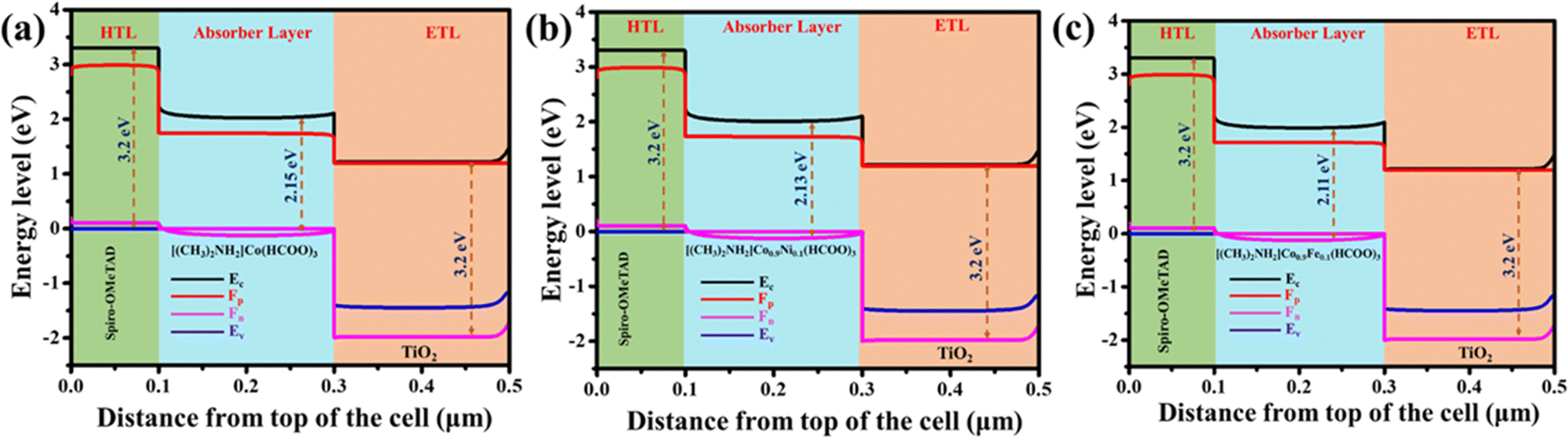
4.7 Energy-band engineering of [(CH3)2NH2]Co(HCOO)3, [(CH3)2NH2]Co0.9Fe0.1(HCOO)3, and [(CH3)2NH2]Co0.9Ni0.1(HCOO)3 solar cells
The function of the layers in a solar cell determines the alignment of energy bands. Hence, the absorbent substance (e.g., perovskite) must possess an energy bandgap that aligns with the optimal conversion efficiency of around 1.5–2.2 eV (Fig. 12a–c). One approach involves incorporating an ETL with a conduction band edge (Ec) that is marginally lower than the Ec of the absorber material. Simultaneously, the ETL possesses a valence-band edge further down than the absorber, which facilitates hole reflection and impedes their migration towards the ETL.48 The absorber is situated on one side of the HTL, whereas the ETL is positioned on the other side of the absorber. The valence-band edge of the HTL exhibits slight elevation compared with the absorber, which facilitates more facile movement of holes towards the HTL. Ec exhibits a greater energy level compared with the absorber, thereby resulting in the repulsion of electrons and impeding their movement inside the HTL. There are two distinct methodologies for aligning the bands accurately. Analyses of these entities can be conducted using a reference level called the “vacuum level”. Before engaging with the contents, the state of alignment must be considered.
 |
| | Fig. 12 Energy-band diagram of different absorbers. (a) [(CH3)2NH2]Co(HCOO)3. (b) [(CH3)2NH2]Co0.9Ni0.1(HCOO)3. (c) [(CH3)2NH2]Co0.9Fe0.1(HCOO)3 in simulated perovskite solar cells. | |
5 Conclusions
We combined experimental, DFT, and drift diffusion-based studies to design, investigate, and optimize [(CH3)2NH2]Co(HCOO)3, [(CH3)2NH2]Co0.9Fe0.1(HCOO)3, and [(CH3)2NH2]Co0.9Ni0.1(HCOO)3 PSCs. Crystals were grown using a solvothermal synthetic route. Crystallographic, morphological, vibrational, and thermal studies of grown crystals were analysed using optical microscopy, spectroscopy (XRD, FT-IR, Raman, UV-Vis), and DSC. Computational studies (band structure, Eigenstates, electron-density profile) confirmed the semiconducting nature of DMACF material. In the next step, PSCs based on [(CH3)2NH2]Co(HCOO)3, [(CH3)2NH2]Co0.9Fe0.1(HCOO)3, and [(CH3)2NH2]Co0.9Ni0.1(HCOO)3 were created. SCAPS modelled the PSCs with drift-diffusion modelling. [(CH3)2NH2]Co(HCOO)3, [(CH3)2NH2]Co0.9Fe0.1(HCOO)3, and [(CH3)2NH2]Co0.9Ni0.1(HCOO)3 absorber layer-based devices with Spiro-OMeTAD as the HTL, TiO2 as the ETL, and platinum as a counter electrode gave efficiencies of 6.44%, 7.20%, and 7.98%, respectively. Extensive experimental research is needed to investigate if Fe- and Ni-substituted perovskite formate crystals can be employed as lead-free absorbers.
Conflicts of interest
The authors declare no conflict of interest.
Acknowledgements
We thank Dr Marc Burgelman of the University of Ghent in Belgium for giving free access to SCAPS 1D. Sathish Marimuthu thanks the DST – PURSE project (India) for funding this research (SR/PURSE/2020/34). The authors extend their appreciation to DST – SERB (India) for funding this research (CRG/2020/005273). The authors extend their appreciation to the Deputyship for Research and Innovation, Ministry of Education in Saudi Arabia for funding this research (IFKSUOR3-122-2).
References
- F. Giustino and H. J. Snaith, Toward lead-free perovskite solar cells, ACS Energy Lett., 2016, 6, 1233–1240 CrossRef.
- B. Hailegnaw, S. Kirmayer, E. Edri, G. Hodes and D. Cahen, Rain on methylammonium lead iodide based perovskites: possible environmental effects of perovskite solar cells, J. Phys. Chem. Lett., 2015, 6, 1543–1547 CrossRef CAS PubMed.
- Z. Shi, J. Guo, Y. Chen, Q. Li, Y. Pan, H. Zhang, Y. Xia and W. Huang, Lead-free organic–inorganic hybrid perovskites for photovoltaic applications: recent advances and perspectives, Adv. Mater., 2017, 29, 1605005 CrossRef PubMed.
- R. Wang, J. Wang, S. Tan, Y. Duan, Z.-K. Wang and Y. Yang, Opportunities and challenges of lead-free perovskite optoelectronic devices, Trends Chem., 2019, 1, 368–379 CrossRef CAS.
- P. Xu, S. Chen, H.-J. Xiang, X.-G. Gong and S.-H. Wei, Influence of defects and synthesis conditions on the photovoltaic performance of perovskite semiconductor CsSnI3, Chem. Mater., 2014, 26, 6068–6072 CrossRef CAS.
- S. Yang, W. Fu, Z. Zhang, H. Chen and C.-Z. Li, Recent advances in perovskite solar cells: efficiency, stability and lead-free perovskite, J. Mater. Chem. A, 2017, 5, 11462–11482 RSC.
- S. F. Hoefler, G. Trimmel and T. Rath, Progress on lead-free metal halide perovskites for photovoltaic applications: a review, Monatsh. Chem., 2017, 148, 795–826 CrossRef CAS PubMed.
- F. Hong, B. Saparov, W. Meng, Z. Xiao, D. B. Mitzi and Y. Yan, Viability of lead-free perovskites with mixed chalcogen and halogen anions for photovoltaic applications, J. Phys. Chem. C, 2016, 120, 6435–6441 CrossRef CAS.
- M. Lyu, J.-H. Yun, P. Chen, M. Hao and L. Wang, Addressing toxicity of lead: progress and applications of low-toxic metal halide perovskites and their derivatives, Adv. Energy Mater., 2017, 7, 1602512 CrossRef.
- M. Lazemi, S. Asgharizadeh and S. Bellucci, A computational approach to interface engineering of lead-free CH3NH3SnI3 highly-efficient perovskite solar cells, Phys. Chem. Chem. Phys., 2018, 20, 25683–25692 RSC.
- M. Chen, Z. Shan, X. Dong, S. F. Liu and Z. Xu, Discovering layered lead-free perovskite solar absorbers via cation transmutation, Nanoscale Horiz., 2023, 8, 483–488 RSC.
- G. K. Grandhi, L. K. Jagadamma, V. Sugathan, B. Al-Anesi, D. Manna and P. Vivo, Lead-free perovskite-inspired semiconductors for indoor light-harvesting–the present and the future, Chem. Commun., 2023, 59, 8616–8625 RSC.
-
S. Marimuthu, S. Sathyanarayanan and A. N. Grace, Reference Module in Earth Systems and Environmental Sciences, Elsevier, 2023 Search PubMed.
- J. Chen, H. Xiang, J. Wang, R. Wang, Y. Li, Q. Shan, X. Xu, Y. Dong, C. Wei and H. Zeng, Perovskite white light emitting diodes: progress, challenges, and opportunities, ACS Nano, 2021, 15, 17150–17174 CrossRef CAS PubMed.
- C.-H. Lin, L. Hu, X. Guan, J. Kim, C.-Y. Huang, J.-K. Huang, S. Singh and T. Wu, Electrode engineering in halide perovskite electronics: plenty of room at the interfaces, Adv. Mater., 2022, 34, 2108616 CrossRef CAS PubMed.
- M. Mączka, A. Sieradzki, B. Bondzior, P. Dereń, J. Hanuza and K. Hermanowicz, Effect of aliovalent doping on the properties of perovskite-like multiferroic formates, J. Mater. Chem. C, 2015, 3, 9337–9345 RSC.
- T. Asaji and K. Ashitomi, Phase Transition and Cationic Motion in a Metal–Organic Perovskite,
Dimethylammonium Zinc Formate [(CH3)2NH2][Zn(HCOO)3], J. Phys. Chem. C, 2013, 117, 10185–10190 CrossRef CAS.
- T. Besara, P. Jain, N. S. Dalal, P. L. Kuhns, A. P. Reyes, H. W. Kroto and A. K. Cheetham, Mechanism of the order–disorder phase transition, and glassy behavior in the metal–organic framework [(CH3)2NH2]Zn (HCOO)3, Proc. Natl. Acad. Sci. U. S. A., 2011, 108, 6828–6832 CrossRef.
- M. K. Hossain, G. I. Toki, A. Kuddus, M. H. K. Rubel, M. M. Hossain, H. Bencherif, M. F. Rahman, M. R. Islam and M. Mushtaq, An extensive study on multiple ETL and HTL layers to design and simulation of high-performance lead-free CsSnCl3-based perovskite solar cells, Sci. Rep., 2023, 13, 2521 CrossRef CAS PubMed.
- S. K. Podapangi, F. Jafarzadeh, S. Mattiello, T. B. Korukonda, A. Singh, L. Beverina and T. M. Brown, Green solvents, materials, and lead-free semiconductors for sustainable fabrication of perovskite solar cells, RSC Adv., 2023, 13, 18165–18206 RSC.
- S. Marimuthu, S. Shriswaroop, M. Muthumareeswaran, S. Pandiaraj, A. N. Alodhayb, T. A. Alrebdi and A. N. Grace, Drift diffusion modelling of cell parameters effect on the performance of perovskite solar cells with MXene as additives, Sol. Energy, 2023, 262, 111804 CrossRef CAS.
- A. P. Shyma and R. Sellappan, Computational Probing of Tin-based Lead-free Perovskite Solar Cells: Effects of Absorber Parameters and Various ETL Materials on Device Performance, Materials, 2022, 15, 7859 CrossRef CAS PubMed.
- K. Liang, L. Huang, T. Wang, C. Wang, Y. Guo, Y. Yue, X. Liu, J. Zhang, Z. Hu and Y. Zhu, Rational design of formamidine tin-based perovskite solar cell with 30% potential efficiency via 1-D device simulation, Phys. Chem. Chem. Phys., 2023, 25, 9413–9427 RSC.
- A. K. Al-Mousoi, M. K. Mohammed, A. Kumar, R. Pandey, J. Madan, D. Dastan, M. K. Hossain, P. Sakthivel and Z. M. Yaseen, Understanding Auger recombination in perovskite solar cells, Phys. Chem. Chem. Phys., 2023, 25, 16459–16468 RSC.
- R. Scatena, R. D. Johnson, P. Manuel and P. Macchi, Formate-mediated magnetic superexchange in the model hybrid perovskite [(CH3)2NH2]Cu(HCOO)3, J. Mater. Chem. C, 2020, 8, 12840–12847 RSC.
- S. A. LoCicero, C. M. Averback, U. Shumnyk, E. S. Choi and D. R. Talham, Particle size effects on the order–disorder phase transition in [(CH3) 2NH2] Mg (HCOO) 3, J. Phys. Chem. C, 2020, 124, 21113–21122 CrossRef CAS.
-
D. Sornadurai, R. M. Sarguna, K. Vinod and V. Sridharan, AIP Conference Proceedings, AIP Publishing, 2019, vol. 2115 Search PubMed.
-
R. A. Laudise and J. W. Nielsen, Solid state physics, Elsevier, 1961, vol. 12, pp. 149–222 Search PubMed.
- T. Nishinaga, Thermodynamics-for understanding crystal growth, Prog. Cryst. Growth Charact. Mater., 2016, 62, 43–57 CrossRef CAS.
- A. Görling, Density-functional theory beyond the Hohenberg-Kohn theorem, Phys. Rev. A: At., Mol., Opt. Phys., 1999, 59, 3359 CrossRef.
- A. Seidl, A. Görling, P. Vogl, J. A. Majewski and M. Levy, Generalized Kohn-Sham schemes and the band-gap problem, Phys. Rev. B: Condens. Matter Mater. Phys., 1996, 53, 3764 CrossRef CAS PubMed.
- M. K. Hossain, M. H. K. Rubel, G. I. Toki, I. Alam, M. F. Rahman and H. Bencherif, Effect of various electron and hole transport layers on the performance of CsPbI3-based perovskite solar cells: A numerical investigation in DFT, SCAPS-1D, and wxAMPS frameworks, ACS Omega, 2022, 7, 43210–43230 CrossRef CAS PubMed.
- Z. M. Baiyee, C. Chen and F. Ciucci, A DFT+U study of A-site and B-site substitution in BaFeO3−δ, Phys. Chem. Chem. Phys., 2015, 17, 23511–23520 RSC.
- Y.-L. Lee, M. J. Gadre, Y. Shao-Horn and D. Morgan, Ab initio GGA+ U study of oxygen evolution and oxygen reduction electrocatalysis on the (001) surfaces of lanthanum transition metal perovskites LaBO 3 (B = Cr, Mn, Fe, Co and Ni), Phys. Chem. Chem. Phys., 2015, 17, 21643–21663 RSC.
-
M. Burgelman, K. Decock, A. Niemegeers, J. Verschraegen and S. Degrave, SCAPS manual, February.
- G. A. Nowsherwan, S. S. Hussain, M. Khan, S. Haider, I. Akbar, N. Nowsherwan, S. Ikram, S. Ishtiaq, S. Riaz and S. Naseem, Role of graphene-oxide and reduced-graphene-oxide on the performance of lead-free double perovskite solar cell, Z. Naturforsch., A: Phys. Sci., 2022, 77(11), 1083–1098 CrossRef CAS.
- A. Bag, R. Radhakrishnan, R. Nekovei and R. Jeyakumar, Effect of absorber layer, hole transport layer thicknesses, and its doping density on the performance of perovskite solar cells by device simulation, Sol. Energy, 2020, 196, 177–182 CrossRef CAS.
- S. Mahjabin, Md. M. Haque, K. Sobayel, M. S. Jamal, M. A. Islam, V. Selvanathan, A. K. Assaifan, H. F. Alharbi, K. Sopian, N. Amin and Md Akhtaruzzaman, Perceiving of Defect Tolerance in Perovskite Absorber Layer for Efficient Perovskite Solar Cell, IEEE Access, 2020, 8, 106346 Search PubMed.
- R. Lindblad, D. Bi, B. Park, J. Oscarsson, M. Gorgoi, H. Siegbahn, M. Odelius, E. M. J. Johansson and H. Rensmo, Electronic Structure of TiO2/CH3NH3PbI3 Perovskite Solar Cell Interfaces, J. Phys. Chem. Lett., 2014, 5, 648–653 CrossRef CAS PubMed.
- A. Kumar, A. Rana, N. Vashistha, K. K. Garg and R. K. Singh, Defect states influencing hysteresis and performance of perovskite solar cells, Sol. Energy, 2020, 211, 345–353 CrossRef CAS.
- J. Shi, J. Dong, S. Lv, Y. Xu, L. Zhu, J. Xiao, X. Xu, H. Wu, D. Li, Y. Luo and Q. Meng, Hole-conductor-free perovskite organic lead iodide heterojunction thin-film solar cells: High efficiency and junction property, Appl. Phys. Lett., 2014, 104, 063901 CrossRef.
- I. Montoya De Los Santos, H. J. Cortina-Marrero, M. A. Ruíz-Sánchez, L. Hechavarría-Difur, F. J. Sánchez-Rodríguez, M. Courel and H. Hu, Optimization of CH3NH3PbI3 perovskite solar cells: A theoretical and experimental study, Sol. Energy, 2020, 199, 198–205 CrossRef CAS.
- S. Asgharizadeh and S. K. Azadi, Additive MXene and dominant recombination channel in perovskite solar cells, Sol. Energy, 2022, 241, 720–727 CrossRef CAS.
-
A. L. Fahrenbruch and R. H. Bube, Survey of basic concepts, in Fundamentals of Solar Cell, ed. A. L. Fahrenbruch and R. H. Bube, 1983, pp. 1–25 Search PubMed.
- P. Chelvanathan, M. I. Hossain and N. Amin, Performance analysis of copper–indium–gallium–diselenide (CIGS) solar cells with various buffer layers by SCAPS, Curr. Appl. Phys., 2010, 10, S387–S391 CrossRef.
- T. Nakada and M. Mizutani, 18% efficiency Cd-free Cu (In, Ga) Se2 thin-film solar cells fabricated using chemical bath deposition (CBD)-ZnS buffer layers, Jpn. J. Appl. Phys., 2002, 41, L165 CrossRef CAS.
- P. Liu, V. P. Singh, C. A. Jarro and S. Rajaputra, Cadmium sulfide nanowires for the window semiconductor layer in thin film CdS-CdTe solar cells, Nanotechnology, 2011, 22, 145304 CrossRef PubMed.
- S. Ijaz, E. Raza, Z. Ahmad, M. Zubair, M. Q. Mehmood, H. Mehmood, Y. Massoud and M. M. Rehman, Numerical simulation to optimize the efficiency of HTM-free perovskite solar cells by ETM engineering, Sol. Energy, 2023, 250, 108–118 CrossRef CAS.
|
| This journal is © the Owner Societies 2024 |
Click here to see how this site uses Cookies. View our privacy policy here. 
 a,
Saravanan
Pandiaraj
b,
Muthumareeswaran
Muthuramamoorthy
a,
Saravanan
Pandiaraj
b,
Muthumareeswaran
Muthuramamoorthy

 is the Coulomb interaction, and Vext(r) is any external potential (e.g., applied external bias potential). Use of the pseudo-potential plane-wave (PP-PW) total energy computation was employed to determine the ground-state structure of [(CH3)2NH2]Co(HCOO)3, [(CH3)2NH2]Co0.9Fe0.1(HCOO)3 and [(CH3)2NH2]Co0.9Ni0.1(HCOO)3 systems. The generalised gradient approximation (GGA) and Perdew–Burke–Ernzerhof functional were used to implement the exchange–correlation potential. A larger k-point grid size (8 × 8 × 8) was used to observe the pattern of electronic charge density.32–34 Utilisation of the Broyden–Fletcher–Goldfarb–Shanno algorithm was crucial for conducting structural optimisation and accurately determining the lattice constants, as well as the internal atomic coordinates of [(CH3)2NH2]Co(HCOO)3, [(CH3)2NH2]Co0.9Fe0.1(HCOO)3, and [(CH3)2NH2]Co0.9Ni0.1(HCOO)3.