Charge doping and electric field tunable ferromagnetism and Curie temperature of the MnS2 monolayer†
Received
10th September 2023
, Accepted 13th November 2023
First published on 14th November 2023
Abstract
Two-dimensional ferromagnets with a long-range ferromagnetic ordering at finite temperature present a bright prospect for their potential applications in nanoscale spintronic devices. The tuning of their intrinsic ferromagnetism and Curie temperature is essential for the development of next-generation data storage and spintronic devices. In this work, the electronic structures, ferromagnetism and Curie temperature of two-dimensional MnS2 monolayer are controlled by charge doping and electric field using first principles calculations. The results show that the dynamic and thermal stability of monolayer MnS2 for all of the cases can be still maintained. Moreover, there is no existence of phase transition and all MnS2 monolayers at any charge doping concentrations and electric field intensities favor ferromagnetic coupling. For the manipulation of electron doping, the calculated total magnetic moment Mtot of the MnS2 monolayer exhibits an increase from 3.112 to 3.491μB per unit cell. Further analysis indicates that a transition from half-metal to metal occurs by introducing the charge doping and vertical electric field, and the Mn 3d electronic states are the major determinants of ferromagnetism. Additionally, the charge doping enables the magnetic anisotropy energy to transform from an in-plane easy axis to the magnetization direction out of the plane. The Curie temperature Tc of the MnS2 monolayer can be moderately enhanced above room temperature by hole doping and application of a vertical electric field. Remarkably, Tc reaches its peak at 767 K at a hole doping concentration of −0.8e. This work enriches the microscopic understanding of the tuning mechanism of ferromagnetism and supplies a sound theoretical basis for subsequent experimental studies.
1. Introduction
Ever since two-dimensional (2D) ferromagnetic (FM) Cr2Ge2Te6 and CrI3 monolayers have been exfoliated successfully in 2017,1,2 there has been growing interest in 2D ferromagnets on account of their exceptional physical characteristics. The 2D ferromagnets display robust magnetic anisotropy, which suppresses the effect of thermal fluctuations on long-range ferromagnetic ordering and breaks the limitation of the Mermin–Wagner theorem,3,4 allowing them to exist at finite temperature. Hence, the 2D FM materials present a bright prospect for their potential applications in nanoscale spintronic devices.5–9
2D transition-metal dichalcogenides (TMDs) have drawn widespread attention ascribable to their fascinating properties and possible applications in integrated circuits, electrocatalysis, photocatalysis, batteries, supercapacitors, sensors and valleytronics.10–19 Among many 2D TMD materials, those with intrinsic ferromagnetism have been highly favored by researchers. Their intrinsic ferromagnetism makes them promising candidates for applications in ultra-compact spintronic devices. A great number of theoretical studies have been done to predict the 2D FM TMDs, such as VX2 (X = S, Se) monolayers,20,21 CrX2 (X = S, Se and Te) monolayers,22,23 Janus TMXX′ (TM = V, Cr and Mn; X, X′ = S, Se and Te, X ≠ X′) monolayers,24–26etc. Experimentally, M. Bonilla et al. reported that monolayer VSe2 with strong ferromagnetic ordering was grown on graphite or MoS2 by molecular beam epitaxy (MBE), and the ferromagnetism with a large magnetic moment persisted to above room temperature.27 D. J. O’Hara et al. described that room temperature ferromagnetism in manganese selenide films grown by MBE was observed, and in the monolayer limit, the ferromagnetism originated from a vdW manganese diselenide (MnSe2) monolayer, while for thicker films it could originate from a combination of vdW MnSe2 and/or interfacial magnetism of α-MnSe(111).28 X. Q. Zhang et al. reported the successful growth of single- and few-layer CrTe2 on bilayer graphene by MBE, and the FM order was preserved with the film thickness down to a monolayer (Curie temperature ∼200 K).29 On the basis of the aforementioned research studies, it is found that the MnS2 monolayer, a typical member of 2D TMDs with intrinsic ferromagnetism, is an appealing material for practical spintronic applications. As far as we know, there are only three reports30–32 regarding the rhombohedral MnS2 monolayer, which highlights the need for further exploration into the tuning of its intrinsic ferromagnetism and Curie temperature, thereby offering a novel orientation for the development of spintronic devices.
The variation of 2D ferromagnetism in few atomic layers is determined by what scheme to tune. These schemes, such as defects, strain, chemical modification, charge doping, electric field, etc., have been affirmed as available approaches. Among them, two widely employed methods (charge doping and electric field) are chosen. The rationale behind this selection is that they can be easily implemented in experiment by applying the gate voltage.33–36 Moreover, the concentration of electron or hole doping has a much great impact on the bond strength of the system, while the positions of the Fermi level and electronic states are altered via the application of an electric field. These two methods are particularly desirable owing to the unique ability to further change their physical properties of FM materials, making them extremely attractive for the realization of prospective low-dimensional spintronic applications. In addition, the effect of charge doping and electric field on the electronic and magnetic properties of the MnS2 monolayer has not been reported previously. Consequently, the electronic structures, ferromagnetism and Curie temperature of single layer MnS2 are controlled by tuning charge doping and external electric field using first principles calculations. This work intends to comprehensively shed light on the tuning mechanism of ferromagnetism from a microscopic perspective, which supplies a sound theoretical basis for subsequent experimental studies.
2. Computational procedures
Our calculations were accomplished by first principles methods based upon density functional theory (DFT), as implemented in the Vienna ab initio simulation package (VASP) code.37,38 The projector augmented wave (PAW) approach39 was applied with a plane wave cutoff energy of 500 eV. The exchange correlation energies were calculated utilizing the generalized gradient approximation (GGA) of the Perdew–Burke–Ernzerhof (PBE) scheme.40 Taking into account the strong interactions of 3d electrons, the spin polarized GGA+U calculations were used with an on-site Coulomb term U value for Mn of 3.9 eV.41–43 A supercell of 2 × 2 × 1 was constructed, and one FM configuration and two antiferromagnetic (AFM) configurations for the MnS2 monolayer were considered. A vacuum space of 20 Å was adopted to eliminate the interactions between two neighboring images. The Monkhorst–Pack44k-point grids of 9 × 9 × 1 and 18 × 18 × 1 were employed in the Brillouin zone for structural relaxation and electronic structure calculations. The convergence criteria for total energies and maximum residual force on each atom were set to 10−6 eV and 10−2 eV Å−1, respectively. The spin orbit coupling (SOC) correction was included in magnetic anisotropy energy (MAE) calculations. The dynamical stability was assessed by analyzing the phonon dispersion spectrum based on the density functional perturbation theory performed in the PHONOPY code.45 The ab initio molecular dynamics (AIMD) simulations in the NVT ensemble using a Nosé–Hoover thermostat were done at a room temperature of 300 K for 10000 steps with a time step of 1 fs to evaluate the thermal stability. The Monte Carlo (MC) method46 was utilized to calculate the Curie temperature of monolayer MnS2 at various charge doping concentrations and electric field intensities on the basis of the Ising model.
3. Results and discussion
3.1 Structural and electronic properties of a pristine MnS2 monolayer
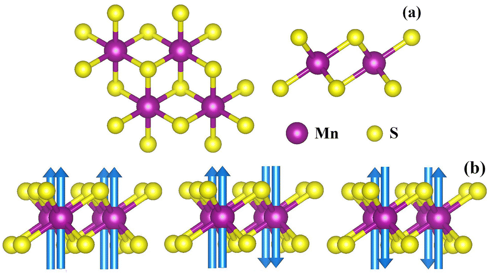
The MnS2 monolayer exhibits a centered honeycomb (T) structure with a space group of R![[3 with combining macron]](https://www.rsc.org/images/entities/char_0033_0304.gif) m (no. 166). Each Mn atom has an octahedral coordination structure with respect to six S atoms surrounding it and each S atom is bonded to three neighbouring Mn atoms. The top view and side view of monolayer MnS2 are shown in Fig. 1(a). There are three magnetic configurations considered in our work, including a FM configuration and two different AFM configurations (AFM1 and AFM2), as illustrated in Fig. 1(b). We perform standard relaxation on the MnS2 monolayer, and the optimized lattice parameter, the bond lengths of Mn–S and S–S, and the bond angle of S–Mn–S are 3.342 Å, 2.371 Å and 3.363 Å, and 89.636°, respectively. These values are consistent with previous calculations.30,31
m (no. 166). Each Mn atom has an octahedral coordination structure with respect to six S atoms surrounding it and each S atom is bonded to three neighbouring Mn atoms. The top view and side view of monolayer MnS2 are shown in Fig. 1(a). There are three magnetic configurations considered in our work, including a FM configuration and two different AFM configurations (AFM1 and AFM2), as illustrated in Fig. 1(b). We perform standard relaxation on the MnS2 monolayer, and the optimized lattice parameter, the bond lengths of Mn–S and S–S, and the bond angle of S–Mn–S are 3.342 Å, 2.371 Å and 3.363 Å, and 89.636°, respectively. These values are consistent with previous calculations.30,31
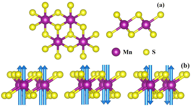 |
| | Fig. 1 Top view and side view of the MnS2 monolayer (a) and FM, AFM1 and AFM2 configurations (b). The arrows on Mn atoms stand for spin orientations. | |
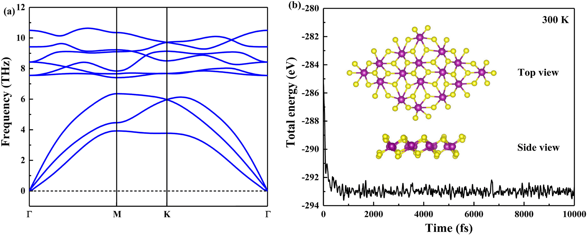
To examine the stability of a primitive MnS2 single layer, the phonon dispersion is calculated first for all k points in the Brillouin zone. The calculated result is displayed in Fig. 2(a). The imaginary phonon modes are not observed, confirming that the MnS2 monolayer is dynamically stable. Furthermore, AIMD simulation is carried out using a 4 × 4 × 1 supercell at 300 K. The relationship curve between the total energies and simulation steps of the MnS2 monolayer is depicted in Fig. 2(b). The fluctuation of total energies is small and the original configuration is well maintained with time evolution. These findings indicate that the pristine MnS2 monolayer has good thermal stability at room temperature.
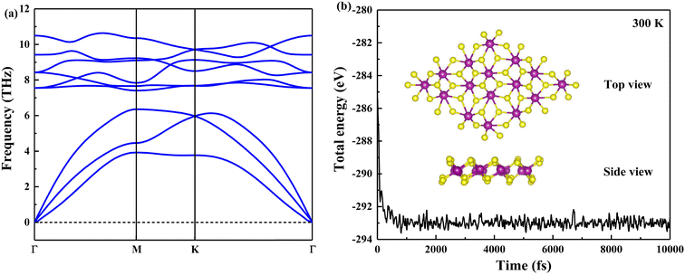 |
| | Fig. 2 The phonon dispersion spectrum (a) and the relationship curve between the total energies and simulation steps (b) of the MnS2 monolayer. The inset is the configuration after AIMD simulation. | |
The spin-polarized band structures and density of states (DOS) of the pristine MnS2 monolayer are diagrammed in Fig. 3. It is worth mentioning that the MnS2 monolayer presents FM half-metallic behavior, where it is metallic in the spin-up sub-band and semiconducting in the spin-down channel with a direct band gap of 1.34 eV. The half-metallicity characterized by a perfect spin polarization of 100% at the Fermi level for the MnS2 monolayer greatly expands its applications in the field of spintronic devices. As can be seen from the DOS of the MnS2 monolayer, the dominant contribution in a lower energy range from −6.6 eV to −4 eV comes from the Mn 3d states and secondarily from the S 3p states. The valence band between −4 eV and −2 eV is primarily originated from the hybridization between the Mn 3d and S 3p orbitals, while the S 3p states dominate the top of the valence band from −2 eV to the Fermi level. On the other hand, the bottom of the conduction band is mainly derived from the Mn 3d orbitals with a little hybridization of S 3p orbitals. The Mn 3d electronic states are the major determinants of ferromagnetism. These results are in accordance with a preceding study.31
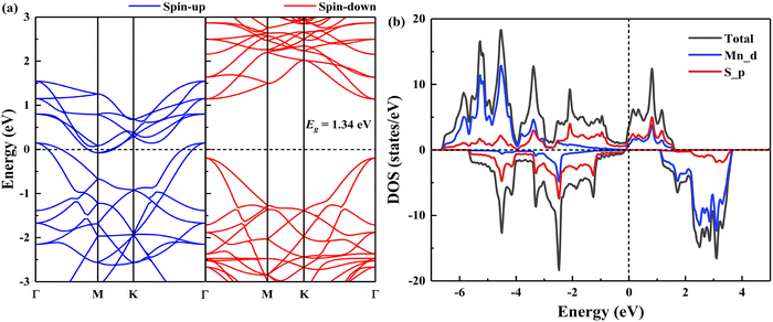 |
| | Fig. 3 The spin-polarized band structures (a) and density of states (b) of the pristine MnS2 monolayer. The short-dashed lines point to the Fermi level. | |
3.2 The effect of charge doping
Charge doping is an effective way of tuning the physical properties of 2D Janus materials.47–49 Motivated by this, the magnetic behavior dependence on charge doping in the MnS2 monolayer is simulated. The electron (hole) doping is carried out via adding (removing) electrons into (from) the system with a compensating uniform charge background of opposite sign.50,51 The stability of monolayer MnS2 at various charge doping concentrations (ranging from −1.0e to 1.0e per unit cell) is evaluated by the phonon dispersion spectra and AIMD simulations, and these results are displayed in Fig. S1 and S2 in ESI.† For all of the cases, they are dynamically and thermally stable.
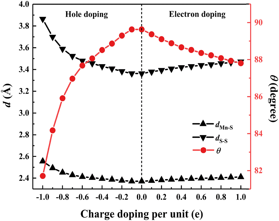
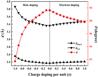
Fig. 4 depicts the optimized bond lengths and bond angles as a function of charge doping concentrations. As can be observed, the bond lengths dMn–S and dS–S all increase, while the bond angle θS–Mn–S decreases as the electron or hole doping concentration enhances. Although the structural parameters show a greater variation with the change in hole doping concentration compared to electron doping, monolayer MnS2 is less likely to undergo the fracture failure of its structure.
 |
| | Fig. 4 The bond lengths and bond angles of monolayer MnS2 at various charge doping concentrations. | |
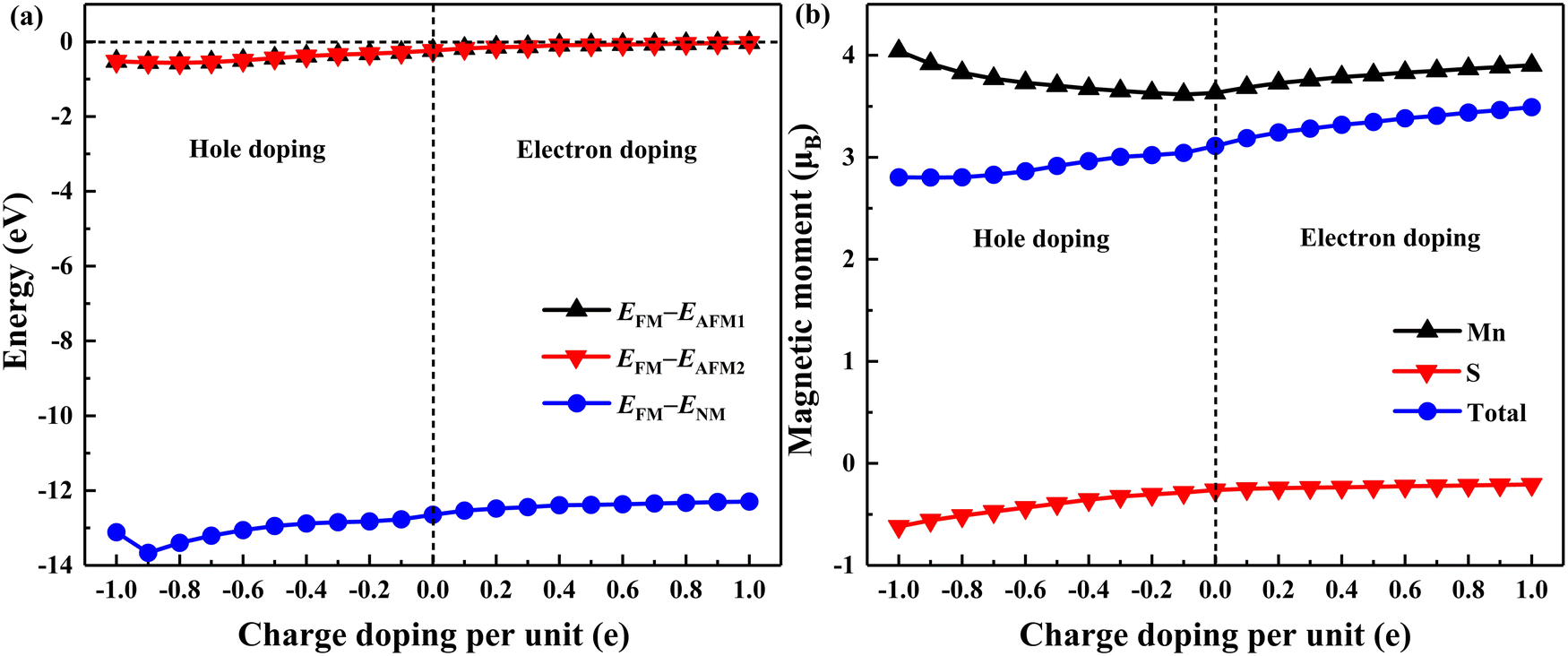
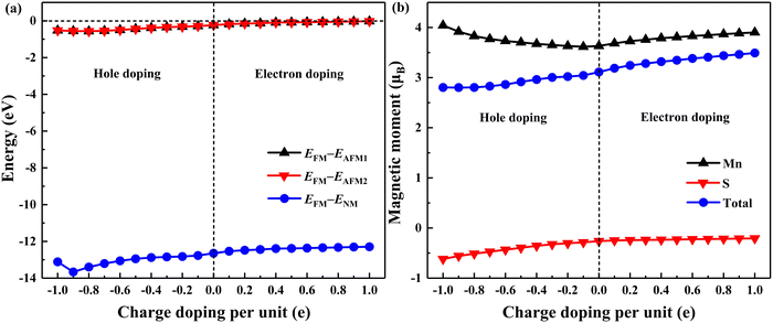
For the purpose of exploring the effect of charge doping on the ground state of the MnS2 monolayer, the charge doping dependence of the total energy differences between FM and AFM1, AFM2, and nonmagnetic (NM) configurations is shown in Fig. 5(a). It is obvious that all total energy differences within the whole range from −1.0e to 1.0e are less than zero, demonstrating that the FM state is still the ground state of monolayer MnS2 at various charge doping concentrations, and there is no existence of phase transition at any concentrations. Furthermore, the FM ordering in monolayer MnS2 is more robust and stable in the presence of electron doping than that in the presence of hole doping. Meanwhile, the magnetic moments of the MnS2 unit cell and Mn and S atoms (Mtot, MMn and MS) at different charge doping concentrations are calculated, as described in Fig. 5(b). The total magnetic moment Mtot of the pristine MnS2 monolayer is 3.112μB per unit cell, close to the earlier results of 3.0μB per unit cell.30,31Mtot is primarily localized at the Mn site with an MMn of 3.632μB and the nearby S atoms are polarized antiferromagnetically with an MS of −0.26μB. Moreover, it is interesting to note that both Mtot and MS increase when the charge doping concentration varies from −1.0e to 1.0e, whereas MMn enhances with the increment of electron or hole doping concentration. These changes in magnetic moments can be attributed to the charge doping manipulation of the bonding strength of covalent bonds in the MnS2 monolayer, which can cause a growth or decline in the amount of unpaired electrons and subsequently affect the variation of magnetic moments.
 |
| | Fig. 5 The energy differences between FM and AFM1, AFM2, and NM configurations (a) and the magnetic moments of the MnS2 unit cell and Mn and S atoms (b) for monolayer MnS2 at various charge doping concentrations. | |
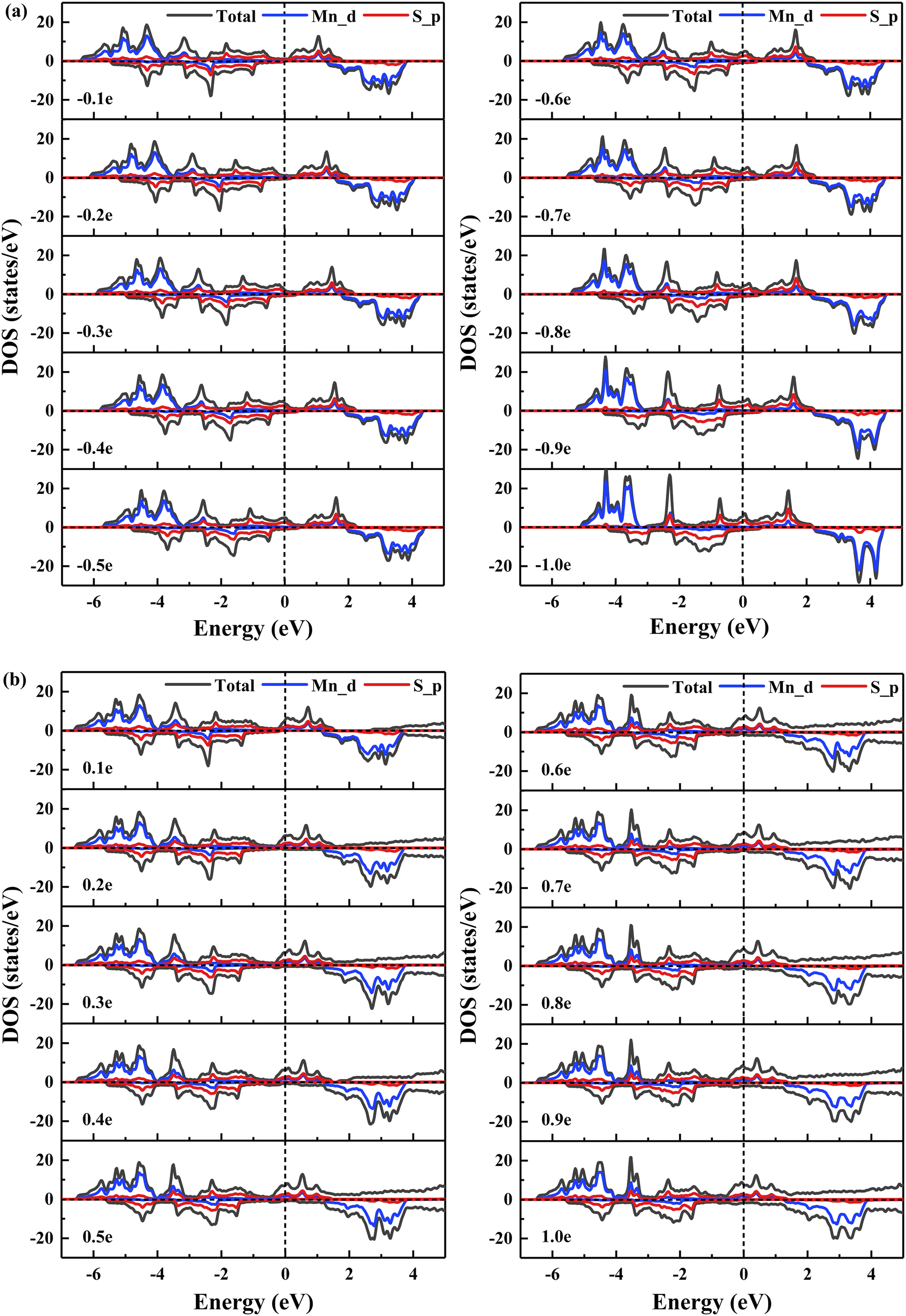
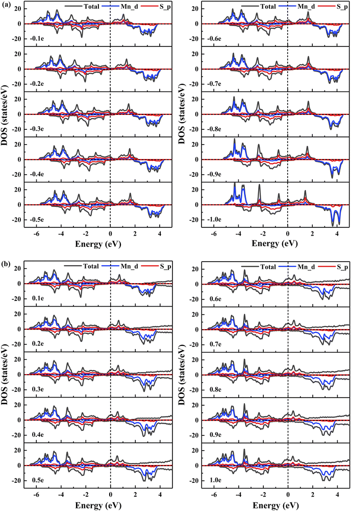
To further probe the influence of charge doping on the electronic structures, the spin-polarized band structures and DOS of monolayer MnS2 at charge doping concentrations ranging from −1.0e to 1.0e are calculated, as plotted in Fig. S3 in ESI† and Fig. 6. One can see that the band gap in the spin-down channel slightly enhances to 1.37 eV and 1.35 eV at the concentrations of −0.1e and 0.1e, respectively. All MnS2 monolayers show metallic nature by continuing to increase the hole or electron doping concentration. Besides, the DOS move towards higher energy zones with the increment of hole doping concentration, indicating a drop in the amount of electrons below the Fermi level, which leads to the structural stability of the system getting bad. The decline in the number of valence electrons as the hole doping concentration rises results in the amount of bonding electrons decreasing. A lower number of bonding electrons causes weaker electrostatic interactions.52 On the contrary, when the electron doping concentration gradually increases from 0.1e to 1.0e, the DOS deviate towards lower energy regions, connoting an increment in the number of electrons below the Fermi level. This induces a more stable structure. The growth in the amount of bonding electrons implies that the interaction of valence electrons is intensified. Additionally, the hybridized states are a main effect for the exchange splitting of these systems,53 and thus, the changes in the ferromagnetism of monolayer MnS2 at various charge doping concentrations can be analyzed by the orbital hybridization. When the concentration of hole doping grows, the hybridization states notably increase, which translates into a perturbation and in turn decreases the exchange splitting in the d orbitals. In contrast, the reduction of the orbital hybridization between the Mn 3d and S 3p electronic states brings about the increase of exchange splitting with the gain of electron doping concentration. This finding is in agreement with the analysis of magnetic moments discussed earlier.
 |
| | Fig. 6 The total and projected DOS of monolayer MnS2 with charge doping concentrations of (a) −0.1 to −1.0e per unit cell and (b) 0.1 to 1.0e per unit cell. The Fermi level is denoted by the short-dashed lines. | |
The restriction of the Mermin–Wagner theorem can be broken by magnetic anisotropy and a long-range ferromagnetic ordering is obtained at finite temperature in 2D ferromagnets.54–56 As a result, the MAE manipulation makes the MnS2 monolayer possess different easy axes, which is significant for its applications in the field of spintronic devices. The MAE can be defined by the following equation:
where
E‖ (
E⊥) stands for the total energy with the magnetization direction parallel (perpendicular) to the surface and the SOC interactions are considered. By tuning the charge doping concentration of the MnS
2 monolayer,
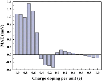
Fig. 7 shows the calculated MAE. A positive MAE value of 0.05616 meV for the primitive MnS
2 monolayer connotes the magnetization direction out of the plane. This MAE value is close to the former result of 0.056 meV.
31 With the electron doping concentration varying from 0.1
e to 0.6
e, the MAE value decreases monotonically and continues to remain positive. Nevertheless, when the concentration of electron doping further increases to 1.0
e, the negative value of MAE suggests that the magnetization direction changes to the in-plane direction. Likewise, the MAE maintains the negative value with the growth of hole doping concentration from −0.1
e to −0.4
e, whereas the easy axis turns perpendicular to the plane with the enhancement of hole doping concentration from −0.5
e to −1.0
e. The charge doping enables the MAE to transform between an in-plane and out-of-plane easy axis, and hole doping is more effective in improving the MAE value compared to electron doping. These results prove that the valid MAE manipulation of the MnS
2 monolayer by charge doping makes it possible to become an ideal magnetic storage spin-electronic material.
 |
| | Fig. 7 The MAE of monolayer MnS2 at various charge doping concentrations. | |
For all MnS2 monolayers with FM coupling at various charge doping concentrations, it is necessary to further discuss their Curie temperature Tc. A Tc above room temperature is a crucial parameter for practical applications in spintronic devices. To this end, the Tc values of monolayer MnS2 with charge doping concentrations ranging from −1.0e to 1.0e per unit cell are evaluated by MC simulations with a 50 × 50 × 1 superlattice using the Ising model. The magnetic coupling Hamiltonian57 can be written as follows:
| |  | (2) |
where
Ji,j represents the nearest-neighboring magnetic exchange parameter,
Si/
Sj is the magnetic moment at the
i/
j site, and 〈
i,
j〉 denotes the nearest-neighbor site pair. In the MnS
2 monolayer, there are six nearest-neighbor spin-parallel Mn atoms per unit cell for FM ordering, while each Mn atom has two nearest-neighbor spin-parallel and four nearest-neighbor spin-antiparallel Mn atoms per unit cell for AFM1/AFM2 coupling. As a consequence, the total energies of FM, AFM1 and AFM2 states obtained from DFT calculations are mapped to the magnetic coupling Hamiltonian [
eqn (2)] to acquire the following expressions:
| | | EAFM1/AFM2 = E0 − 2J|S|2 + 4J|S|2 = E0 + 2J|S|2 | (4) |
where
E0 stands for the total energy independent of the magnetic coupling and the magnetic moment
S is equal to 3.0
μB. The nearest-neighboring magnetic exchange parameter
J can be gained from the total energy differences between FM and AFM ordering. In the MC simulations, the spins on all magnetic sites turn randomly and the calculations last for 10
5 steps for each temperature. The results of MC simulations are displayed in
Fig. 8.
Tc can be estimated by observing a noticeable drop in the magnetic moment
M or locating the peak position of specific heat
Cv. The calculated
Tc of the pristine MnS
2 monolayer is as high as 317 K after our correction of coupling interaction, higher than the previous result of 225 K.
30 By introducing the charge doping,
Tc monotonically decreases and falls below room temperature with the increment of electron doping concentration, whereas it ascends quickly to the highest value of 767 K and then slightly declines as the hole doping concentration grows. According to a prior study on tuning the
Tc of the MnS
2 monolayer
via applying in-plane biaxial strain, it is found that strain engineering is an efficient approach to enhance the magnetic coupling of 2D MnS
2 by using substrate lattice mismatching, and
Tc can be increased to 330 K under 5% strain.
30 In comparison with the strain manipulation, the hole doping is also more readily achieved in experiment and exhibits a stronger control effect on the
Tc of the MnS
2 monolayer (a significant increase in the
Tc). This implies that the tuning of hole doping is desirable for improving the spin coupling of the MnS
2 monolayer, thereby making it an appealing candidate for spintronic applications.
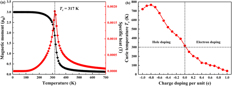 |
| | Fig. 8 The temperature dependence of the magnetic moment and specific heat of the MnS2 monolayer (a) and the Curie temperature of monolayer MnS2 at various charge doping concentrations (b). | |
3.3 The effect of external electric field
As is well known, the physical properties of 2D van der Waals materials are highly sensitive to external impacts.58–60 Therefore, the influence of external electric field on the magnetic properties of the MnS2 monolayer is also investigated in the follow-up work. A series of electric fields along the positive z-axis within the range from 0.1 to 1.5 eV Å−1 are applied in the MnS2 monolayer. It is worth noting that the vertical electric field does not induce any geometric distortion. In the meantime, the FM coupling of monolayer MnS2 remains unchanged after imposing the electric field ranging from 0.1 to 1.5 eV Å−1, which is ascribed to the negative total energy differences between FM and AFM1/AFM2/NM configurations (see Table 1). Furthermore, the total and local magnetic moments of monolayer MnS2 at different electric field intensities are also listed in Table 1. As can be seen, the Mtot and MMn are almost constant with the intensity of electric field varying from 0.1 to 0.9 eV Å−1, whereas a small decline in these values is observed as the electric field strength keeps growing. This manifests that a large enough electric field intensity is required to induce changes in the magnetic moments of the MnS2 monolayer.
Table 1 The energy differences between FM and AFM1, AFM2, and NM configurations, the magnetic moments of the MnS2 unit cell, Mn and S atoms, the MAE, nearest-neighbor magnetic exchange parameters, and the Curie temperature of monolayer MnS2 at different electric field intensities
| Electric field (eV Å−1) |
E
FM − EAFM1 (eV) |
E
FM − EAFM2 (eV) |
E
FM − ENM (eV) |
M
tot (μB) |
M
Mn (μB) |
M
S (μB) |
MAE (meV) |
J (meV) |
T
c (K) |
| 0.1 |
−0.23458 |
−0.23460 |
−12.64501 |
3.112 |
3.632 |
−0.260 |
0.14607 |
0.83248 |
321 |
| 0.2 |
−0.23464 |
−0.23465 |
−12.64564 |
3.112 |
3.632 |
−0.256/−0.264 |
0.23958 |
0.83300 |
321 |
| 0.3 |
−0.23473 |
−0.23475 |
−12.64636 |
3.112 |
3.632 |
−0.254/−0.266 |
0.33311 |
0.83365 |
321 |
| 0.4 |
−0.23487 |
−0.23488 |
−12.64758 |
3.112 |
3.632 |
−0.252/−0.268 |
0.42681 |
0.83444 |
321 |
| 0.5 |
−0.23504 |
−0.23506 |
−12.64922 |
3.112 |
3.632 |
−0.250/−0.270 |
0.52055 |
0.83538 |
321 |
| 0.6 |
−0.23526 |
−0.23528 |
−12.65108 |
3.112 |
3.632 |
−0.248/−0.272 |
0.61453 |
0.83645 |
321 |
| 0.7 |
−0.23552 |
−0.23553 |
−12.65332 |
3.112 |
3.632 |
−0.246/−0.274 |
0.70882 |
0.83766 |
321 |
| 0.8 |
−0.23581 |
−0.23582 |
−12.65569 |
3.112 |
3.632 |
−0.244/−0.276 |
0.80372 |
0.83902 |
321 |
| 0.9 |
−0.23641 |
−0.23642 |
−12.65877 |
3.110 |
3.631 |
−0.243/−0.278 |
0.86417 |
0.84152 |
321 |
| 1.0 |
−0.24601 |
−0.24596 |
−12.67332 |
3.102 |
3.627 |
−0.245/−0.280 |
0.83919 |
0.87477 |
337 |
| 1.1 |
−0.25417 |
−0.25409 |
−12.68585 |
3.097 |
3.625 |
−0.246/−0.282 |
0.85366 |
0.90328 |
345 |
| 1.2 |
−0.26159 |
−0.26148 |
−12.69764 |
3.093 |
3.623 |
−0.246/−0.284 |
0.87215 |
0.92931 |
353 |
| 1.3 |
−0.26852 |
−0.26844 |
−12.70920 |
3.088 |
3.621 |
−0.247/−0.286 |
0.89220 |
0.95353 |
361 |
| 1.4 |
−0.27508 |
−0.27511 |
−12.72049 |
3.084 |
3.619 |
−0.247/−0.288 |
0.91108 |
0.97676 |
377 |
| 1.5 |
−0.28146 |
−0.28150 |
−12.73169 |
3.079 |
3.618 |
−0.248/−0.291 |
0.92738 |
0.99902 |
385 |
The application of an external electric field is a valid method to modulate the Fermi level and electronic states of the structure. The spin-polarized band structures of monolayer MnS2 under the influence of different electric fields are illustrated in Fig. S4 in ESI.† From the results, it is clear that the MnS2 monolayer is still a half-metal with a spin-down band gap of 1.34 eV as the vertical electric field varies from 0.1 to 0.8 eV Å−1, which is in conformity with the band gap of single layer MnS2 without an electric field. The band gap of the spin-down channel descends from 1.34 to 0.19 eV at an electric field intensity of 0.9 eV Å−1. A transition from half-metal to metal occurs at an electric field strength of 1.0 eV Å−1, and the MnS2 monolayer retains the metallic feature under the vertical electric field ranging from 1.0 to 1.5 eV Å−1. These results demonstrate that the position of the Fermi level moving up with the growth of electric field intensity leads to an increase in the occupation of valence bands by electrons, thereby inducing charge redistribution in these systems.61–63
To gain insight into the electric field dependence of MAE for the MnS2 monolayer, the calculated MAE values are shown in Table 1. The positive values of MAE within the whole range of electric field mean that the magnetization is oriented out of plane, which accounts for the electric field direction along the z-axis. The MAE value of the MnS2 monolayer is improved via the application of a vertical electric field. Additionally, the magnetic exchange interaction J and Curie temperature Tc are also analyzed for all MnS2 monolayers under different electric field strengths, as shown in Table 1. When the vertical electric field varies from 0.1 to 0.9 eV Å−1, a slight variation in the magnetic coupling makes the Tc remain at 321 K. J and Tc can reach 0.999 meV and 385 K with an increasing intensity of the electric field from 1.0 to 1.5 eV Å−1. Compared to the control of hole doping, a sufficiently high electric field intensity is needed to attain a small growth in the Tc. Importantly, for all of these MnS2 monolayers imposed by the electric field, the Tc values are higher than room temperature, which connotes that the MnS2 monolayer via tuning of electric field can be considered in practical applications in the field of spintronics.
4. Conclusions
This work aims at performing a thorough analysis of tuning the electronic structures, ferromagnetism and Curie temperature of the MnS2 monolayer by electron–hole doping and applying an external electric field using first principles methods based on DFT. Firstly, all MnS2 monolayers at various charge doping concentrations and electric field strengths are dynamically and thermally stable. Moreover, there is no existence of phase transition and all MnS2 monolayers at any charge doping concentrations and electric field intensities favor the FM coupling. For the control of electron doping, the calculated total magnetic moment Mtot of the MnS2 monolayer exhibits an enhancement from 3.112 to 3.491μB per unit cell. Meanwhile, a large enough electric field intensity of 1.0 eV Å−1 is required to induce change in the magnetic moment of the MnS2 monolayer. Furthermore, a transition from half-metal to metal occurs by introducing the charge doping and vertical electric field, and the Mn 3d electronic states are the major determinants of ferromagnetism. In addition, the MAE manipulation enables the MnS2 monolayer to possess different easy axes. The positive MAE values at the concentrations of −0.5 to −1.0e and 0–0.6e connote the magnetization direction out of the plane, whereas the MAE retaining the negative values at the concentrations of −0.1 to −0.4e and 0.7–1.0e suggests an in-plane easy axis. By applying a vertical electric field, the MAE value is improved and remains positive. Finally, the Tc of the MnS2 monolayer can be moderately increased above room temperature by hole doping and application of a vertical electric field. The highest Tc of 767 K is obtained at a hole doping concentration of −0.8e. These results demonstrate that the MnS2 monolayer via tuning of charge doping and electric field has great potential for applications in nanoscale spintronic devices. This research is beneficial for supplying a sound theoretical reference for the following experimental studies.
Author contributions
Jing Xie: conceptualization, methodology, validation, investigation, data curation, writing – original draft, writing – reviewing and editing, funding acquisition; Dongni Wu: formal analysis, writing – reviewing and editing, supervision; Yangfang Liao: methodology, formal analysis, investigation, writing – reviewing and editing; Xiaolong Cao: validation, software; and Shiyou Zhou: resources, data curation.
Conflicts of interest
There are no conflicts to declare.
Acknowledgements
This work was supported by the Guizhou Provincial Science and Technology Foundation [Grant No. ZK[2023]247] and Academic New Seedling Program of Guizhou Normal University, China [Grant No. [2021]B13].
References
- C. Gong, L. Li, Z. L. Li, H. W. Ji, A. Stern, Y. Xia, T. Cao, W. Bao, C. Z. Wang, Y. Wang, Z. Q. Qiu, R. J. Cava, A. G. Louie, J. Xia and X. Zhang, Discovery of intrinsic ferromagnetism in two-dimensional van der Waals crystals, Nature, 2017, 546(7657), 265–269, DOI:10.1038/nature22060.
- B. Huang, G. Clark, E. Navarromoratalla, D. R. Klein, R. Cheng, K. L. Seyler, D. Zhong, E. Schmidgall, M. A. Mcguire, D. H. Cobden, W. Yao, D. Xiao, P. Jarilloherrero and X. D. Xu, Layer-dependent ferromagnetism in a van der Waals crystal down to the monolayer limit, Nature, 2017, 546(7657), 270–273, DOI:10.1038/nature22391.
- N. D. Mermin and H. Wagner, Absence of ferromagnetism or antiferromagnetism in one- or two-dimensional isotropic Heisenberg models, Phys. Rev. Lett., 1966, 17, 1133–1136, DOI:10.1103/PhysRevLett.17.1133.
- P. C. Hohenberg, Existence of long-range order in one and two dimensions, Phys. Rev., 1967, 158, 383–386, DOI:10.1103/PhysRev.158.383.
- P. Huang, P. Zhang, S. G. Xu, H. D. Wang, X. W. Zhang and H. Zhang, Recent advances in two-dimensional ferromagnetism: materials synthesis, physical properties and device application, Nanoscale, 2020, 12, 2309–2327, 10.1039/C9NR08890C.
- H. Wang, X. Y. Li, Y. Wen, R. Q. Cheng, L. Yin, C. S. Liu, Z. W. Li and J. He, Two-dimensional ferromagnetic materials: from materials to devices, Appl. Phys. Lett., 2022, 121, 220501, DOI:10.1063/5.0130037.
- S. S. Liu, K. Yang, W. Q. Liu, E. Zhang, Z. H. Li, X. Q. Zhang, Z. M. Liao, W. Zhang, J. B. Sun, Y. K. Yang, H. Gao, C. Huang, L. F. Ai, P. K. J. Wong, A. T. S. Wee, A. T. N. Diaye, S. A. Morton, X. F. Kou, J. Zou, Y. B. Xu, H. Wu and F. X. Xiu, Two-dimensional ferromagnetic superlattices, Natl. Sci. Rev., 2020, 7(4), 745–754, DOI:10.1093/nsr/nwz205.
- B. Shabbir, M. Nadeem, Z. G. Dai, M. S. Fuhrer, Q. K. Xue, X. L. Wang and Q. L. Bao, Long range intrinsic ferromagnetism in two dimensional materials and dissipationless future technologies, Appl. Phys. Rev., 2018, 5, 041105, DOI:10.1063/1.5040694.
- S. Yu, J. Y. Tang, Y. Wang, F. X. Xu, X. G. Li and X. Z. Wang, Recent advances in two-dimensional ferromagnetism: strain-, doping-, structural- and electric field-engineering toward spintronic applications, Sci. Technol. Adv. Mater., 2022, 23(1), 140–160, DOI:10.1080/14686996.2022.2030652.
- S. Das, A. Sebastian, E. Pop, C. J. McClellan, A. D. Franklin, T. Grasser, T. Knobloch, Y. Illarionov, A. V. Penumatcha, J. Appenzeller, Z. Chen, W. J. Zhu, I. Asselberghs, L. J. Li, U. E. Avci, N. Bhat, T. D. Anthopoulos and R. Singh, Transistors based on two-dimensional materials for future integrated circuits, Nat. Electron., 2021, 4, 786–799, DOI:10.1038/s41928-021-00670-1.
- D. Akinwande, C. Huyghebaert, C. H. Wang, M. I. Serna, S. Goossens, L. J. Li, H. S. P. Wong and F. H. L. Koppens, Graphene and
two-dimensional materials for silicon technology, Nature, 2019, 573, 507–518, DOI:10.1038/s41586-019-1573-9.
- C. R. Zhu, D. Q. Gao, J. Ding, D. L. Chao and J. Wang, TMD-based highly efficient electrocatalysts developed by combined computational and experimental approaches, Chem. Soc. Rev., 2018, 47, 4332–4356, 10.1039/C7CS00705A.
- R. J. Yang, Y. Y. Fan, Y. F. Zhang, L. Mei, R. S. Zhu, J. Q. Qin, J. G. Hu, Z. X. Chen, Y. H. Ng, D. Voiry, S. Li, Q. Y. Lu, Q. Wang and J. C. Yu, 2D transition metal dichalcogenides for photocatalysis, Angew. Chem., Int. Ed., 2023, 62(13), e202218016, DOI:10.1002/anie.202218016.
- S. P. Wu, Y. Du and S. J. Sun, Transition metal dichalcogenide based nanomaterials for rechargeable batteries, Chem. Eng. J., 2017, 307, 189–207, DOI:10.1016/j.cej.2016.08.044.
- L. X. Lin, W. Lei, S. W. Zhang, Y. Q. Liu, G. G. Wallace and J. Chen, Two-dimensional transition metal dichalcogenides in supercapacitors and secondary batteries, Energy Storage Mater., 2019, 19, 408–423, DOI:10.1016/j.ensm.2019.02.023.
- N. Rohaizad, C. C. Mayorga-Martinez, M. Fojtů, N. M. Latiff and M. Pumera, Two-dimensional materials in biomedical, biosensing and sensing applications, Chem. Soc. Rev., 2021, 50, 619–657, 10.1039/D0CS00150C.
- J. F. Ping, Z. X. Fan, M. Sindoro, Y. B. Ying and H. Zhang, Recent advances in sensing applications of two-dimensional transition meral dichalcogenide nanosheets and their composites, Adv. Funct. Mater., 2017, 27(19), 1605817, DOI:10.1002/adfm.201605817.
- C. Tan, X. Cao, X. J. Wu, Q. He, J. Yang, X. Zhang, J. Chen, W. Zhao, S. Han and G. H. Nam, Recent advances in ultrathin two-dimensional nanomaterials, Chem. Rev., 2017, 117, 6225–6331, DOI:10.1021/acs.chemrev.6b00558.
- K. F. Mak, K. He, J. Shan and T. F. Heinz, Control of valley polarization in monolayer MoS2 by optical helicity, Nat. Nano., 2012, 7, 494–498, DOI:10.1038/nnano.2012.96.
- Y. D. Ma, Y. Dai, M. Guo, C. W. Niu, Y. T. Zhu and B. B. Huang, Evidence of the existence of magnetism in pristine VX2 monolayers (X = S, Se) and their strain-induced tunable magnetic properties, ACS Nano, 2012, 6(2), 1695–1701, DOI:10.1021/nn204667z.
- N. Luo, C. Si and W. H. Duan, Structural and electronic phase transitions in ferromagnetic monolayer VS2 induced by charge doping, Phys. Rev. B, 2017, 95, 205432, DOI:10.1103/PhysRevB.95.205432.
- C. Wang, X. Zhou, Y. Pan, J. Qiao, X. Kong, C. C. Kaun and W. Ji, Layer and doping tunable ferromagnetic order in two-dimensional CrS2 layers, Phys. Rev. B, 2018, 97(24), 245409, DOI:10.1103/PhysRevB.97.245409.
- H. Y. Lv, W. J. Lu, D. F. Shao, Y. Liu and Y. P. Sun, Strain-controlled switch between ferromagnetism and antiferromagnetism in 1T-CrX2 (X = Se, Te) monolayers, Phys. Rev. B: Condens. Matter Mater. Phys., 2015, 92, 214419, DOI:10.1103/PhysRevB.92.214419.
- J. J. He and S. Li, Two-dimensional Janus transition-metal dichalcogenides with intrinsic ferromagnetism and half-metallicity, Comput. Mater. Sci., 2018, 152, 151–157, DOI:10.1016/j.commatsci.2018.05.049.
- S. M. Qi, J. W. Jiang and W. B. Mi, Tunable valley polarization, magnetic anisotropy and Dzyaloshinskii–Moriya interaction in two-dimensional intrinsic ferromagnetic Janus 2H-VSeX (X = S, Te) monolayers, Phys. Chem. Chem. Phys., 2020, 22, 23597–23608, 10.1039/D0CP03292A.
- M. Abdollahi and M. B. Tagani, Tuning intrinsic ferromagnetic and anisotropic properties of the Janus VSeS monolayer, J. Mater. Chem. C, 2020, 8, 13286–13296, 10.1039/D0TC03147J.
- M. Bonilla, S. Lolekar, Y. J. Ma, H. C. Diaz, V. Kalappattil, R. Das, T. Eggers, H. R. Gutierrez, M. H. Phan and M. Batzill, Strong room-temperature ferromagnetism in VSe2 monolayers in van der Waals substrates, Nat. Nanotechnol., 2018, 13, 289–293, DOI:10.1038/s41565-018-0063-9.
- D. J. O'Hara, T. Zhu, A. H. Trout, A. S. Ahmed, Y. K. Luo, C. H. Lee, M. R. Brenner, S. Rajan, J. A. Gupta, D. W. McComb and R. K. Kawakami, Room temperature intrinsic ferromagnetism in epitaxial manganese selenide films in the monolayer limit, Nano Lett., 2018, 18(5), 3125–3131, DOI:10.1021/acs.nanolett.8b00683.
- X. Q. Zhang, Q. S. Lu, W. Q. Liu, W. Niu, J. B. Sun, J. Cook, M. Vaninger, P. F. Miceli, D. J. Singh, S. W. Lian, T. R. Chang, X. Q. He, J. Du, L. He, R. Zhang, G. Bian and Y. B. Xu, Room-temperature intrinsic ferromagnetism in epitaxial CrTe2 ultrathin films, Nat. Commun., 2021, 12, 2492, DOI:10.1038/s41467-021-22777-x.
- M. Kan, S. Adhikari and Q. Sun, Ferromagnetism in MnX2 (X = S, Se) monolayers, Phys. Chem. Chem. Phys., 2013, 4(20), 3382–3386, 10.1039/C3CP55146F.
- Y. L. Yue, Electronic and magnetic properties of monolayer MnS2, Mod. Phys. Lett. B, 2016, 30(36), 1650419, DOI:10.1142/s021798491650419.
- C. H. Shen, G. T. Wang, T. X. Wang, X. Zhao, Y. Yan, X. H. Song, X. Y. Liu, Y. Wang and C. X. Xia, Tuning the magnetic anisotropy of ferromagnetic MnS2 monolayers via electron occupation of Mn d orbitals, Phys. Rev. B, 2021, 104, 224406, DOI:10.1103/PhysRevB.104.224406.
- Y. J. Deng, Y. J. Yu, Y. C. Song, J. Z. Zhang, N. Z. Wang, Z. Y. Sun, Y. F. Yi, Y. Z. Wu, S. W. Wu, J. Y. Zhu, J. Wang, X. H. Chen and Y. B. Zhang, Gate-tunable room-temperature ferromagnetism in two-dimensional Fe3GeTe2, Nature, 2018, 563, 94–99, DOI:10.1038/s41586-018-0626-9.
- S. W. Jiang, L. Z. Li, Z. F. Wang, K. F. Mak and J. Shan, Controlling magnetism in 2D CrI3 by electrostatic doping, Nat. Nanotechnol., 2018, 13, 549–553, DOI:10.1038/s41565-018-0135-x.
- B. Huang, G. Clark, D. R. Klein, D. MacNeill, E. Navarro-Moratalla, K. L. Seyler, N. Wilson, M. A. McGuire, D. H. Cobden, D. Xiao, W. Yao, P. Jarillo-Herrero and X. Xu, Electrical control of 2D magnetism in bilayer CrI3, Nat. Nanotechnol., 2018, 13, 544–548, DOI:10.1038/s41565-018-0121-3.
- S. Jiang, J. Shan and K. F. Mak, Electric-field switching of two-dimensional van der Waals magnets, Nat. Mater., 2018, 17, 406–410, DOI:10.1038/s41563-018-0040-6.
- G. Kresse and J. Hafner, Ab initio molecular dynamics for liquid metals, Phys. Rev. B: Condens. Matter Mater. Phys., 1993, 47(1), 558–561, DOI:10.1103/PhysRevB.47.558.
- G. Kresse and J. Furthmüller, Efficient iterative schemes for ab initio total-energy calculations using a plane-wave basis set, Phys. Rev. B: Condens. Matter Mater. Phys., 1996, 54(16), 11169–11186, DOI:10.1103/PhysRevB.54.11169.
- P. E. Blöchl, Projector augmented-wave method, Phys. Rev. B: Condens.
Matter Mater. Phys., 1994, 50, 17953–17979, DOI:10.1103/PhysRevB.50.17953.
- J. P. Perdew, K. Burke and M. Ernzerhof, Generalized gradient approximation made simple, Phys. Rev. Lett., 1996, 77, 3865–3868, DOI:10.1103/PhysRevLett.77.3865.
- L. Wang, T. Maxisch and G. Ceder, Oxidation energies of transition metal oxides within the GGA+U framework, Phys. Rev. B: Condens. Matter Mater. Phys., 2006, 73, 195107, DOI:10.1103/PhysRevB.73.195107.
- C. Ling and F. Mizuno, Capture lithium in αMnO2: insights from first principles, Chem. Mater., 2012, 24, 3943–3951, DOI:10.1021/cm302347j.
- M. Kan, J. Zhou, Q. Sun, Y. Kawazoe and P. Jena, The intrinsic ferromagnetism in a MnO2 monolayer, J. Phys. Chem. Lett., 2013, 4, 3382–3386, DOI:10.1021/jz4017848.
- H. J. Monkhorst and J. D. Pack, Special points for Brillouin-zone integrations, Phys. Rev. B: Condens. Matter Mater. Phys., 1976, 13, 5188–5192, DOI:10.1103/PhysRevB.13.5188.
- A. Togo and I. Tanaka, First principles phonon calculations in materials science, Sci. Mater., 2015, 108, 1–5, DOI:10.1016/j.scriptamat.2015.07.021.
- L. Liu, S. Chen, Z. Lin and X. Zhang, A symmetry-breaking phase in two-dimensional FeTe2 with ferromagnetism above room temperature, J. Phys. Chem. Lett., 2020, 11, 7893–7900, DOI:10.1021/acs.jpclett.0c01911.
- T. Cao, Z. L. Li and S. G. Louie, Tunable magnetism and half-metallicity in hole-doped monolayer GaSe, Phys. Rev. Lett., 2015, 114, 236602, DOI:10.1103/PhysRevLett.114.236602.
- J. J. Chen, K. Wu, H. H. Ma, W. Hu and J. L. Yang, Tunable Rashba spin splitting in Janus transition-metal dichalcogenide monolayers via charge doping, RSC Adv., 2020, 10, 6388–6394, 10.1039/d0ra00674b.
- L. Y. Zhu, Y. Lu and L. Wang, Tuning ferroelectricity by charge doping in two-dimensional SnSe, J. Appl. Phys., 2020, 127, 014101, DOI:10.1063/1.5123296.
- C. Si, W. H. Duan, Z. Liu and F. Liu, Electronic strengthening of graphene by charge doping, Phys. Rev. Lett., 2012, 109, 226802, DOI:10.1103/PhysRevLett.109.226802.
- P. H. Sun, J. F. Zhang, K. Liu, Q. Han and Z. Y. Lu, First-principles study of the superconductivity in LaO, Phys. Rev. B, 2021, 104, 045121, DOI:10.1103/PhysRevB.104.045121.
- R. Ma, Q. Xie and J. Huang, Electronic structure and ferromagnetism of Fe11NiSi4, Fe11CoSi4, Fe11CrSi4 and Fe3Si from first principles, Intermetallics, 2014, 46, 12–17, DOI:10.1016/j.intermet.2013.10.021.
- Y. Zhou, Z. Wang, P. Yang, X. Zu, L. Yang, X. Sun and F. Gao, Tensile strain switched ferromagnetism in layered NbS2 and NbSe2, ACS Nano, 2012, 6, 9727–9736, DOI:10.1021/nn303198w.
- J. L. Lado and J. Fernández-Rossier, On the origin of magnetic anisotropy in two dimensional CrI3, 2D Mater., 2017, 4(3), 035002, DOI:10.1088/2053-1583/aa75ed.
- J. Liu, M. Shi, J. Lu and M. P. Anantram, Analysis of electrical-field-dependent dzyaloshinskii-moriya interaction and magnetocrystalline anisotropy in a two-dimensional ferromagnetic monolayer, Phys. Rev. B, 2018, 97, 054416, DOI:10.1103/PhysRevB.97.054416.
- N. Richter, D. Weber, F. Martin, N. Singh, U. Schwingenschlögl, B. V. Lotsch and M. Kläui, Temperature dependent magnetic anisotropy in the layered magnetic semiconductors CrI3 and CrBr3, Phys. Rev. Mater., 2018, 2, 024004, DOI:10.1103/PhysRevMaterials.2.024004.
- J. Zhou and Q. Sun, Magnetism of phthalocyanine-based organometallic single porous sheet, J. Am. Chem. Soc., 2011, 133(38), 15113–15119, DOI:10.1021/ja204990j.
- J. Li, W. Q. Liu, W. H. Zhou, J. L. Yang, H. Z. Qu, Y. Hu and S. L. Zhang, Dipole-engineering strategy for regulating the electronic contact of a two-dimensional SbX/Graphene (X = P, As, Bi) van der Waals interface, Phys. Rev. Appl., 2022, 17, 054009, DOI:10.1103/PhysRevApplied.17.054009.
- J. Li, W. H. Zhou, L. L. Xu, J. L. Yang, H. Z. Qu, T. T. Guo, B. Xu, S. L. Zhang and H. B. Zeng, Revealing the weak Fermi level pinning effect of 2D semiconductor/2D metal contact: a case of monolayer In2Ge2Te6 and its Janus structure In2Ge2Te3Se3, Mater. Today Phys., 2022, 26, 100749, DOI:10.1016/j.mtphys.2022.100749.
- J. Li, X. Y. Guo, X. M. Hu, W. Wang, Y. Y. Tai, M. Xie, Z. Li, S. L. Zhang and H. B. Zeng, Realization of multifunction in perovskite-based van der Waals heterostructure by interface engineering strategy: the case of CsPbBr3/Janus MoSSe, Appl. Surf. Sci., 2023, 618, 156626, DOI:10.1016/j.apsusc.2023.156626.
- L. Xie and J. Zhu, The electronic structures, born effective charges, and interatomic force constants in BaMO3 (M = Ti, Zr, Hf, Sn): a comparative first-principles study, J. Am. Ceram. Soc., 2012, 95, 3597–3604, DOI:10.1111/j.1551-2916.2012.05371.x.
- D. D. Vo, T. V. Vu, S. A. Qaisi, H. D. Tong, T. S. Le, C. V. Nguyen, H. V. Phuc, H. L. Luong, H. R. Jappor, M. M. Obeid and N. N. Hieu, Janus monolayer PtSSe under external electric field and strain: a first principles study on electronic structure and optical properties, Superlattices Microstruct., 2020, 147, 106683, DOI:10.1016/j.spmi.2020.106683.
- M. Luo and Y. E. Xu, Tunable band-gap of the GeC monolayer by strain and electric field: a first-principles study, Optik, 2019, 195, 163147, DOI:10.1016/j.ijleo.2019.163147.
|
| This journal is © the Owner Societies 2024 |
Click here to see how this site uses Cookies. View our privacy policy here. 
 *,
Dongni
Wu
,
Yangfang
Liao
,
Xiaolong
Cao
and
Shiyou
Zhou
*,
Dongni
Wu
,
Yangfang
Liao
,
Xiaolong
Cao
and
Shiyou
Zhou