
 Open Access Article
 This Open Access Article is licensed under a Creative Commons Attribution-Non Commercial 3.0 Unported Licence
Enhancing electrocatalytic activity in metallic thin films through surface segregation of carbon†
Ayesha
Kousar
 a,
Ulviyya
Quliyeva
a,
Ishan
Pande
a,
Jani
Sainio
b,
Jaakko
Julin
c,
Timo
Sajavaara
c,
Antti J.
Karttunen
d and
Tomi
Laurila
*ad
a,
Ulviyya
Quliyeva
a,
Ishan
Pande
a,
Jani
Sainio
b,
Jaakko
Julin
c,
Timo
Sajavaara
c,
Antti J.
Karttunen
d and
Tomi
Laurila
*ad
aDepartment of Electrical Engineering and Automation, School of Electrical Engineering, Aalto University, PO Box 13500, 00076 Aalto, Finland. E-mail: tomi.laurila@aalto.fi
bDepartment of Applied Physics, School of Science, Aalto University, PO Box 15100, 00076 Aalto, Finland
cDepartment of Physics, University of Jyväskylä, PO Box 35, FI-40014, Finland
dDepartment of Chemistry and Materials Science, School of Chemical Engineering, Aalto University, PO Box 16100, 00076 Aalto, Finland
First published on 12th December 2023
Abstract
Thin layers of commonly used adhesion metals i.e., Cr and Ti were annealed to investigate and estimate their impact on the electrochemical properties of the carbon nanomaterials grown on top of them. The microstructure, surface chemistry, and electrochemical activities of these materials were evaluated and compared with those of as-deposited thin films. The results from X-ray photoelectron spectroscopy (XPS), Raman spectroscopy, grazing incidence X-ray diffraction (GIXRD), time-of-flight elastic recoil detection analysis (TOF-ERDA), and conductive atomic force microscopy (C-AFM) indicated the formation of a catalytic graphite layer on Cr following annealing, while no such layer was formed on Ti. This is attributed to the formation of the Cr2O3 layer on annealed Cr, which acts as a barrier to carbon diffusion into the underlying Cr. Conversely, Ti exhibits a high solubility for both carbon and oxygen, preventing the formation of the graphite layer. Cyclic voltammetry results showed that annealed Cr electrodes are electrochemically active towards both dopamine (DA) and ascorbic acid (AA) while no electrochemical activity is exhibited by annealed Ti. Quantum chemical calculations suggested that the presence of carbon as graphene or an amorphous form is critical for the oxidation reaction of probes. These results are significant for comprehending how the distinct solubilities of typical interstitial solutes influence the microstructure of adhesion metal layers and consequently yield diverse electrochemical properties.
Introduction
Metal-coated semiconductor substrates are being employed in the field of semiconductor manufacturing, microelectronics, MEMS, solar cell fabrication, thin film deposition, and fabrication of carbon nanostructures.1–6 Seed metal layers (e.g., Ni and Pd) acting as catalysts are utilized for the nucleation and growth of carbon atoms to form carbon nanofibers (CNFs), which have various applications in biosensing, energy storage, electrocatalysis, and electrosorption.7–9 To mitigate issues of delamination, peeling, and device performance degradation caused by poor adhesion of seed layers to the substrate, the use of an adhesion layer between the seed layer and the substrate becomes necessary.10,11 Cr and Ti are among the most commonly used adhesion layers due to their ability to chemically bind with the substrate and provide electrical contact.12 Upon exposure to high temperatures, thin layers undergo significant microstructural changes as they dissolve common atmospheric elements, such as oxygen, carbon, and nitrogen. Furthermore, they exhibit the tendency to diffuse in the substrate materials forming different phases that can lead to changes in resistance, mechanical strength, surface properties, etc.12–16 However, limited research exists on the specific microstructural changes in metallic layers and their influence on the electrochemical activity of carbon nanofibers and electrochemical systems utilizing these layers. Furthermore, the advantages of utilizing specific materials as adhesion layers in the electrochemical setups remain ambiguous.In our previous reports, we evaluated the effect of Cr and Ti adhesion layers in addition to the catalyst layer on the surface chemistry and microstructure of CNFs.7,16 The CNFs grown at the Cr and Ni interface showed a higher population density and a different CNF structure resembling herringbone patterns, whereas CNFs grown at the Ti and Ni interface had a bamboo-like structure and exhibited distinct electrochemical properties.16,17 This pointed out that the role of the interfacial layer is critical and must be understood in detail. However, the comparison of the systems with different adhesion layers is difficult to realize when CNFs are present on the interface presenting the lack of susceptibility to the measurement of underlying layer activity. The systematic study of the metallic layers used as adhesion layers is important to answer several unanswered questions such as (I) how does the microstructural evolution of underlying adhesion layers differ when subjected to similar conditions as used for growing CNFs? (II) Is the electrochemical activity of electrodes is coming from the varying surface properties of underlying adhesion layers? (III) How do both systems interact with the oxygen and carbon contaminants? Obtaining answers to these critical questions is essential for gaining a comprehensive understanding of the complex interface associated with CVD-grown CNFs. It also plays a decisive role in our efforts to optimize material designs that promote the enhanced growth of CNFs and improve their electrochemical activity.
Herein, we have annealed commonly used Ti (20 nm) and Cr (80 nm) adhesion layers at a similar temperature (600 °C) as well as under similar conditions (except the presence of reactive gases and plasma) that we use for growing CNFs for 20 min. The effect of changes in their microstructure and surface chemistry on their electrochemical properties was correlated and compared. According to the best of our knowledge, there has not been any reported systematic analysis of the electrochemical properties of commonly used adhesion layers and their microstructure when catalyst layers are not present, and the varying impacts of contaminants on these metallic layers. The results presented in this manuscript would provide a stepping-stone in understanding the Ti and Cr systems and guide the selection of adhesion layers tailored to specific applications, further enhancing the overall performance of the systems.
Experimental procedures
Metal deposition and annealing
Metal layers (80 nm Cr, 20 nm Ti) were deposited on the Si substrate by the e-beam evaporation technique using a physical vapor deposition (PVD) system (Angstrom Engineering). The samples were annealed using a chemical vapor deposition (CVD) reactor (Aixtron Black Magic). The CVD functionality was disabled and only the heating function was used to prepare the annealed samples. The chamber was pumped after loading the samples. Next, the temperatures were increased to 395 °C at a ramp rate of 250 °C per minute and then to 600 °C at a ramp rate of 300 °C per minute. The samples were annealed at 600 °C for 20 min. A pressure of 0.05–0.07 mbar was maintained during annealing. After the annealing step, Ar was injected into the chamber, and it was allowed to cool down to 150 °C. The samples were then removed from the chamber.XPS
X-Ray photoelectron spectroscopy (XPS) was carried out with a Kratos Axis Ultra spectrometer with monochromated Al Kα-radiation, a pass energy of 40 eV, an X-ray power of 75 W and an analysis area of approximately 700 μm × 300 μm. The binding energy scale was based on instrument calibration and no additional binding energy correction was applied to the data. The elemental composition was determined from peak areas of high-resolution core-level spectra after Shirley background subtraction using equipment specific sensitivity factors. Peak fitting was done using Gaussian–Lorentzian peaks (GL (30) line shape in CasaXPS) with the positions of the peaks fixed within ±0.1 eV of given binding energies. For sp2 carbon, an asymmetric line shape was used in CasaXPS.18 The full widths at half-maximum (FWHMs) of the peaks were restricted to be equal within a fit with the exception of the sp2 carbon peak and the metal oxide peak in the O 1s spectra.TOF-ERDA
The samples were measured using a ToF-ERDA system with beams of 11.9 MeV 63Cu6+ (Ti samples) and 13.6 MeV 63Cu7+ (Cr samples). The scattering angle of the used telescope was 40.6° and the angle between the incident beam and the sample surface was either 20° (Cr samples) or 12° (Ti samples). No significant changes, e.g. loss of hydrogen due to ion bombardment, were detected during the measurements. Analysis was performed using Potku.19Raman spectroscopy
Raman spectroscopy was performed with micro-Raman spectroscopy (WITec Alpha RA+) equipped with an optical microscope. An objective lens of 50× and a laser with an excitation wavelength of 532 nm were used. A single spectrum with 10 accumulations was captured using an integration time of 0.5 s.GIXRD
Thin films were analyzed with a Rigaku Smartlab Diffractometer at OtaNano center, Aalto University. SmartLab RIGAKU has a rotating anode X-ray goniometer with a Cu X-ray source (45 kV and 200 mA). The wavelength employed was the copper K-α1 wavelength (λ = 1.541 Å). The instrument was operated in the grazing incidence mode at room temperature where the incidence slit (IS) was calculated based on the critical angle found from the X-ray reflection measurement. The following equation was used: IS = FP × sin![[thin space (1/6-em)]](https://www.rsc.org/images/entities/char_2009.gif) ω, where FP is the sample's footprint and ω is the critical angle. The optics configuration utilized was PB (parallel beam), length limiting slit was 5 or 10 mm, incident slit box, receiving slit was 1:12 mm, receiving slit was 2:20.1 mm, and a 2D hybrid pixel detector in 1D mode. X-ray fluorescence reduction mode was used. The 2θ range data were collected from 20° to 100° with a scan step of 0.1. To avoid forbidden Si peaks, a phi of 8–10° was used. No background correction was done to the data.
ω, where FP is the sample's footprint and ω is the critical angle. The optics configuration utilized was PB (parallel beam), length limiting slit was 5 or 10 mm, incident slit box, receiving slit was 1:12 mm, receiving slit was 2:20.1 mm, and a 2D hybrid pixel detector in 1D mode. X-ray fluorescence reduction mode was used. The 2θ range data were collected from 20° to 100° with a scan step of 0.1. To avoid forbidden Si peaks, a phi of 8–10° was used. No background correction was done to the data.
Electrochemistry
The cyclic voltammetry technique was used for the electrochemical measurements. 1 mM Ascorbic acid and 100 μM dopamine hydrochloride (Sigma Aldrich) were used as analytes and phosphate buffer solution (PBS) was used as an electrolyte. The recipe for PBS preparation was given elsewhere.8 The measurements were carried out in an electrochemical glass cell using an Ag/AgCl as a reference electrode and platinum wire as a counter electrode. Uncompensated resistance for each sample was measured. The electrochemical cell was purged with N2 for 10 min before the measurements.Electrodes were positioned onto conductive copper sheets (0.3 mm thick double-sided FR4 glass fiber substrates). An inert PTFE tape (Saint-Gobain Performance Plastics CHR 2255-2) enclosed the sample, featuring a 3 mm hole (radius = 1.5 mm). This hole defined the electrode's active area and isolated copper from the electrolyte. Back-side scratching of the carbon sample using copper plate enhanced the substrate–carbon contact.
Quantum chemical calculations
Quantum chemical calculations were carried out with the CRYSTAL23 program package,20 using the hybrid PBE0 density functional method (DFT-PBE0)21 and localized Gaussian-type triple-ζ-valence polarization (TZVP) basis sets.22 The crystal structures of Cr2O3 and TiO2 were taken from a previous DFT-PBE0 study on d-metal oxides (the antiferromagnetic spin-polarized ground state was used for Cr2O3).22 For amorphous carbon, we used a model of graphitic amorphous carbon created by Deringer et al. (200 atoms in the unit cell, model 2.00/10 in the original paper).23 The model structure was fully optimized with the DFT-PBE0 method with D3 dispersion correction (zero-damping).24 Tight tolerance factors (TOLINTEG) of 8, 8, 8, 8, and 16 were used for the evaluation of the Coulomb and exchange integrals. Default CRYSTAL23 structural optimization convergence criteria and DFT integration grids were used. The following Monkhorst–Pack type k-meshes were used in the DFT calculations: 6 × 6 × 6 for Cr2O3, 6 × 6 × 10 for TiO2, 12 × 12 for graphene, and 2 × 2 × 2 for amorphous carbon. A Fermi smearing of 0.001 a.u. (315 K) was applied for graphene and amorphous carbon. For density of states (DOS) calculations, four times denser k-meshes were applied and the DOS were expanded with 12 Legendre polynomials as implemented in crystals.Results and discussion
Microstructure analysis and surface chemistry
XPS was used to study the surface chemistry changes in Cr/Si and Ti/Si thin layers after annealing compared to those in as-deposited films (Fig. 1A–D and Fig. S1, Table S1, ESI†). Peak fitting was utilized for carbon and oxygen spectra to highlight these changes. C 1s spectra have been fitted with six components: sp2 carbon (284.6 eV); sp3 carbon (285.1 eV), which could include contributions from sp2 C–N bonds; C–O–C and/or C–OH (286.6 eV), which could include contributions from sp3 C–N bonds; C![[double bond, length as m-dash]](https://www.rsc.org/images/entities/char_e001.gif) O (288.1 eV), O–CO (289.1 eV) and a π–π* shake up transition (291.0 eV).25,26 The rather broad O 1s peak (Fig. 1B) has been fitted with three components corresponding to metal–oxygen (O–M) bonds (530.5 eV), OC bonds (531.9 eV) and O–C and/or OH–C bonds (533.2 eV).25,27
O (288.1 eV), O–CO (289.1 eV) and a π–π* shake up transition (291.0 eV).25,26 The rather broad O 1s peak (Fig. 1B) has been fitted with three components corresponding to metal–oxygen (O–M) bonds (530.5 eV), OC bonds (531.9 eV) and O–C and/or OH–C bonds (533.2 eV).25,27
 | ||
| Fig. 1 X-Ray photoelectron spectra of Cr/Si and Ti/Si before and after annealing: (A) C 1s region; (B) O 1s region, (C) Cr 2p region and (D) Ti 2p region. Raman spectra of (E) Cr/Si and (F) Ti/Si before and after annealing. | ||
As shown in Fig. 1A, annealing affects both types of metal layers differently; carbon on the Ti layer before and after annealing remains mainly in the sp3 hybridized form. However, in the case of Cr, the sp2 hybridized component increases significantly as a result of annealing in comparison to as-deposited Cr indicating the presence of a surface region rich in graphitic carbon.28 Fitted results show that there is a high concentration of metal–oxygen (O–M) bonds in both Cr and Ti samples regardless of annealing, indicating that the surface is rich in oxygen. The chromium 2p spectrum in Fig. 2C before annealing shows two 2p3/2 peaks which represent the presence of metallic Cr (574.2 eV) and Cr2O3 (577.0 eV).18,29 In the case of Ti, a small peak at 454.0 eV is also found in Ti/Si, which represents the presence of metallic Ti18 (Fig. 2D). After annealing, both types of samples show peaks related to oxides of Cr and Ti without the presence of the metallic form.
 | ||
| Fig. 2 GIXRD patterns (A and B) and TOF-ERDA depth profiles (C–F) of Cr/Si and Ti/Si before and after annealing. | ||
These results indicate that both metal layers show different affinities for carbon and oxygen as a result of annealing, and the Cr surface is richer with sp2 hybridized carbon. However, on the Ti/Si annealed surface, less carbon is present, and the bonding configuration of carbon does not change as a result of annealing in contrast to the Cr sample. The Ti/Si annealed sample contains an overall higher amount of oxygen in comparison to the Cr surface.
Raman spectroscopy was carried out to further evaluate the chemistry of these metal layers near the surface using a visible excitation wavelength of 532 nm (Fig. 1E and F). Non-annealed Cr/Si shows a low intensity peak at 650 cm−1, indicative of Cr2O3 while no other notable Raman active region can be seen (Fig. 1E). We did not see any other band corresponding to the metallic form of chromium perhaps due to the Raman inactive nature of Cr. After 20 minutes of annealing, Cr shows a prominent G band at 1576 cm−1, which corresponds to the symmetric E2g mode commonly found in graphite-like materials. In addition, a D band at 1363 cm−1 is observed, indicating the presence of grain boundaries or imperfections, such as substitutional nitrogen (N) atoms, sp3 carbon, and impurities30 (Fig. 1E). A broad 2D peak at around 2800 cm−1 and ID/IG > 1 indicate the presence of graphitic carbon with structural disorder and defects.31 The broad peaks indicate that graphite is in the form of microcrystallites.32,33 A sharp peak at around 664 cm−1 and a small shoulder at 553 cm−1 in the Cr/Si annealed sample indicate the presence of Cr2O3 in annealed Cr.34,35 The shift in the Cr2O3 peak could be indicating the phase transitions in the annealed samples in comparison to Cr/Si due to the exposure to high temperatures.36
No graphene layer/amorphous carbon is found in Ti before or after annealing (Fig. 1F). The peaks in the region 200–900 cm−1 are the characteristic of the silicon substrate. It is possible that the titanium oxide phase on the silicon substrate is not Raman active or the Si signal is masking the signals from Ti oxides, leading to the absence of distinct peaks. An increase in the Si band could also be due to the higher transparency of the film owing to the metal film becoming thinner as a result of annealing.30 Furthermore, R. J. Nemanich et al., reported that the enhancement of the Si signal occurs as a result of the diffusion of Si to the surface forming crystalline domains as a preceding step to the formation of silicides.37 According to the Ti–Si phase diagram (Fig. S2, ESI†), the formation of silicides is possible around 600 °C; however, the presence of oxygen impurities may delay the formation of Ti silicides to 750 °C.37 Overall, the Raman results indicate that surface carbon is higher in annealed Cr in comparison to annealed Ti samples.
GIXRD was carried out to study the changes in the microstructure in the surface region (Fig. 2A and B). According to GIXRD patterns, Cr/Si before annealing possesses chromium in the metallic form, which oxidizes on annealing.38,39 Formation of CrN is also taking place on the annealed Cr layer as apparent from the XRD spectra.40 The small peaks at around 50–55° are due to reflections of 311 planes of the Si(100) substrate. In the case of HCP-Ti, metallic Ti could be changing into Ti oxides and suboxides on annealing.41,42 The small and broad peaks indicate the presence of a mixture of the solid solution of elements and (sub)-oxides. As can be seen in the Ti–O phase diagram (Figure S3), Ti forms various suboxides at 600 °C. The graphitic carbon detected in XPS and Raman spectra was not evident in GIXRD data. Nonetheless, it is important to bear in mind that XPS and Raman spectroscopy are more sensitive to surface carbon compared to GIXRD. The penetration depths of X-rays in GIXRD of the Cr and Ti films are calculated to be about 7 nm and 12 nm, respectively.43 It is reported that the X-rays penetrate deeper into the sample and that there can be a contribution from the surface beneath the penetration depth towards the XRD signal.44 Moreover, XPS and TOF-ERDA (Fig. 2) results suggest the presence of a thin oxide layer already formed atop these metallic layers, which becomes thicker during annealing. TOF-ERDA results also indicate the presence of nitrogen which is in the form of CrN suggested by XPS (Fig. S1, ESI†) and GIXRD analyses.
TOF-ERDA was carried out to further analyze the different solubility profiles of carbon and oxygen in Ti and Cr as a result of annealing. The ToF-ERDA results also pointed towards the thickness of deposited layers of Cr and Ti to be similar to what we aimed for. The Ti and Cr coverage values are found to be 19.2 and 78 nm respectively calculated from depth profiles at an atomic concentration (1015 atoms per cm2) with the uncertainty of a few nm involved. Both Cr/Si and Ti/Si showed the presence of carbon on the magnitude of typical surface contamination. However, the Cr/Si annealed sample contains a carbon layer near the surface. Furthermore, the solubility of oxygen is also lower than that in the case of annealed Cr/Si. Thus, in the case of Cr, it seems that the low solubility of oxygen leads to the formation of Cr2O3 on the surface region. This Cr2O3 layer acts as a partial diffusion barrier for carbon, which tends to favor the gettering of carbon on the surface. This is supported by the uneven distribution of O in the case of Cr. It is well-established that the solubility of carbon in Cr2O3 is extremely low or negligible.45 The formation of Cr2O3 at the Cr surface causes a drastic reduction in carbon solubility causing the carbon to segregate to the surface. The reduced bulk solubility of carbon also prevents it from diffusing into the Cr layer. Hence, the diffusion barrier properties of Cr2O3 could play an important role in the segregation of carbon on the surface.
On the other hand, Ti dissolves much larger amounts of oxygen and carbon than Cr. In the case of annealed Ti/Si, the whole Ti layer is saturated with oxygen resulting in the formation of TixO2−x in addition to the solid solutions of Ti, O, C, and N. There is also no strong carbon surface peak like in the Cr case. The solubility of interstitial solute elements in α-Ti is reported to be very high for O, C, and N.46 These results point towards the enhanced carbon solubility in titanium, in comparison to its solubility in chromium, holding significant implications. This distinction becomes evident immediately in the as-deposited films, where the Ti/Si demonstrates thorough saturation with carbon. This saturation appears to yield a more uniform carbon profile than observed in Cr/Si. Furthermore, in the case where Ti/Si attains a state of near-saturation with carbon following deposition, there exists no driving force for carbon diffusion into the film. This absence of a driving force is due to the equalized chemical potential of carbon at the surface and within the film. In the case of annealed Ti/Si, additional oxides form during annealing, and the tendency for carbon segregation to the surface is relatively small. This reduction occurs due to the capacity of the bulk material to dissolve the carbon content present within the volume where the new phase precipitates.47–49 This behavior stands in contrast to the situation with Cr2O3 where a pronounced segregation tendency prevails, owing to the very small solubility of carbon. Hence, these arguments collectively suggest that a more obvious change in the carbon distribution upon annealing can be expected in the case of chromium as opposed to titanium.
C-AFM of the metal layers before and after annealing was conducted to study the changes in the conductance of the materials (Fig. S4, ESI†). Before annealing, both Ti/Si and Cr/Si possess similar topography and the conductance of the samples is also in a similar range. In the case of the Cr annealed surface, the conductance of the sample increased with some conductive patches becoming apparent. The apparent highly conductive regions are likely to segregate carbon on the surface (Fig. S4, ESI†). In TOF-ERDA results, the carbon peak at the surface in the annealed Cr/Si sample is wider for C to be uniformly distributed on the sample surface. This could be explained by lateral inhomogeneity, e.g. patches of thicker carbon. The Ti/Si annealed surface is also showing some conductive regions. Titanium suboxides are considered higher in conductivity than TiO2,50 and the presence of high conductive regions could be due to the higher conductance of TixO2−x.
Electrochemistry
In order to analyze and study the potential contribution of the adhesion layer, we studied the electrochemical activity of these layers before and after annealing (Fig. 3 and Table 1). We used DA and AA as analytes as we have studied the electrochemical activity of these biomolecules on carbon nanofibers grown on similar systems containing these adhesion layers in previous reports.8,16 Both Cr/Si and Ti/Si before annealing could not detect either ascorbic acid or dopamine on their surface. After annealing, Ti/Si does not show any electrochemical activity (Fig. 3A and C). The literature shows that TiO2 in the anatase form shows better electrochemical activity than the rutile phase.51 However, we did not see any crystalline form of TiO2 in any of the particular forms that may have imparted the electrochemical activity to the electrode surface. The Cr/Si annealed electrode shows a broad oxidation peak at 319 ± 135 mV, the characteristic of AA oxidation (Fig. 3B). The annealed Cr/Si surface also exhibits electrochemical activity towards the DA redox reaction showing an oxidation peak potential (Epa) of 220 ± 18 mV with a peak separation (ΔEp = Epa − Epc) of 101 ± 25 mV (Fig. 3D). These results indicate that the presence of a carbon layer is crucial in the electrochemical activity of metal layers. The presence of the high oxygen content on the surface region makes the graphite layer rich in oxygen. Oxygen functional groups are reported to reduce the activation energy for the DA redox reaction by making the proton tunneling strongly adiabatic.52 The DA reaction kinetics on the annealed Cr/Si electrode are similar to the pyrolytic carbon (PyC). On a PyC electrode surface, the DA reaction is reported to be highly dependent on the amount of oxygen and the nature of oxygen functional groups.53 The cyclic voltammetry response of the Cr/Si annealed sample is provided for 10 cycles at 100 mV s−1 in 100 μM DA (Fig. S5A, ESI†), indicating that the response remains similar after several cycles. A slight decrease in the current is expected as the DA on the surface gets depleted and the scan rate outruns the DA diffusion rate to the surface. The slope of logIpavs. logv < 0.5 (Fig. S5B, ESI†) indicates that the graphite layer may not be covering the entire surface and the surface is acting as a partly blocked electrode. The presence of random highly conductive spots seen in C-AFM is consistent with this behavior (Fig. S4, ESI†). The observed electroactive nature of the Cr/Si annealed electrode is likely due to the adsorption of DA on the conductive patches of graphite formed on the electrode surface. The pure electron transfer activity of annealed Cr/Si and Ti/Si electrodes was analyzed by conducting cyclic voltammetry using an outer sphere probe [Ru(NH3)6Cl] in the absence of the surface functionalities involved in the redox reaction (Fig. S6, ESI†). Cyclic voltammograms for the Ti/Si annealed electrode show an irreversible reaction in the absence of a well-defined oxidation peak. The Cr/Si annealed electrode, on the other hand, shows a reversible redox reaction with well-defined oxidation and reduction peaks. These results again indicated the crucial role of precipitated graphite in electron transfer also in the absence of adsorption (with the OSR probe).
 | ||
| Fig. 3 Cyclic voltammetry responses of Ti/Si and Cr/Si before and after annealing in 1 mM ascorbic acid (A) and (C) and 100 μM dopamine (B) and (D) in the PBS electrolyte at a scan rate of 100 mV s−1. | ||
| Samples | I pa (μA) | I pc (μA) | E pa (mV) | E pc (mV) | ΔEp (mV) | logIpavs. logv |
|
|---|---|---|---|---|---|---|---|
| Cr/Si annealed | 100 μM DA | 1.7 ± 0 | 1.4 ± 0.3 | 220 ± 18 | 120 ± 7 | 101 ± 25 | 0.34 ± 0.03 |
| 1 mM AA | 3.85 ± 0.83 | — | 319 ± 135 | — | — | — | |
| Cr/Si | 100 μM DA | No peak | |||||
| 1 mM AA | |||||||
| Ti/Si annealed | 100 μM DA | No peak | |||||
| 1 mM AA | |||||||
| Ti/Si | 100 μM DA | No peak | |||||
| 1 mM AA | |||||||
Quantum chemical calculations
To gain a deeper comprehension of how carbon segregation influences the electrochemical oxidation of ascorbic acid, we carried out quantum chemical calculations for the electronic density of states (DOS) on various materials—Cr2O3, TiO2, graphene, and amorphous carbon. The latter possesses a mass density of 2.3 g cm−3 and is juxtaposed with the highest occupied molecular orbital (HOMO) and lowest unoccupied molecular orbital (LUMO) levels of the initial reduced form of ascorbic acid in the solution. The outcomes are illustrated in Fig. 4.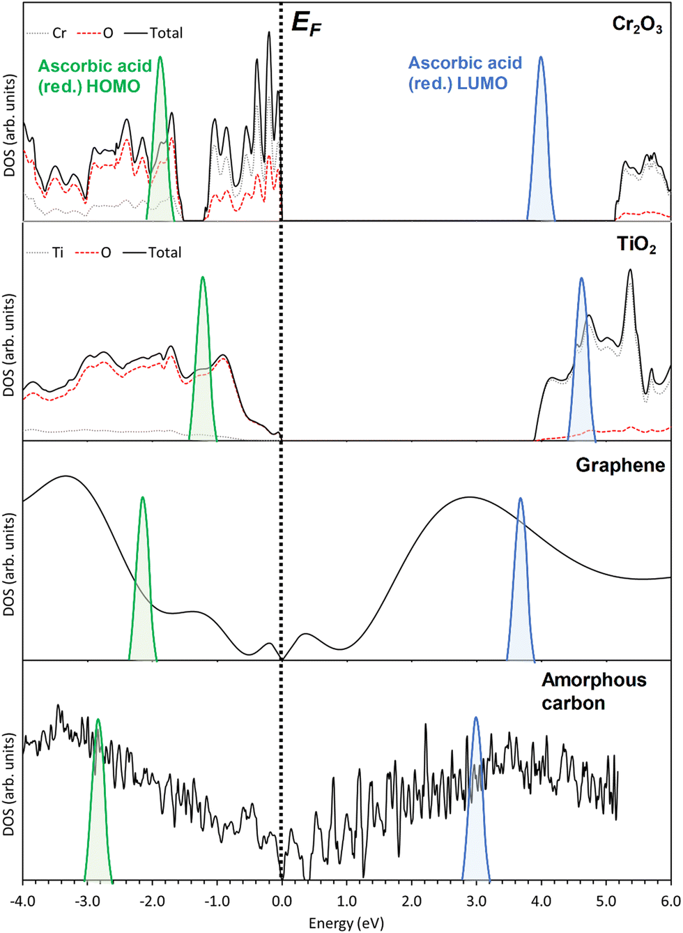 | ||
| Fig. 4 Electronic density of states for Cr2O3, TiO2, graphene, and amorphous carbon. The Fermi level (EF) of all materials has been aligned to the zero level. The HOMO and LUMO levels of ascorbic acid (AA) in its reduced form are illustrated with green and blue Gaussians, respectively. Their positions are drawn with respect to the Fermi level of each individual material. | ||
As the electrode is progressively polarized in an anodic direction, the Fermi level of the respective electrode material shifts towards the left side of the diagram in Fig. 4. As soon as the HOMO level of ascorbic acid aligns with this shifted level, the oxidation process becomes feasible. The figure elucidates that although amorphous carbon necessitates the highest overpotential for ascorbic acid oxidation, it exhibits the most substantial DOS in the vicinity of the Fermi level, thus serving as an optimal recipient of electrons produced during the oxidation reaction of ascorbic acid. Graphene also facilitates the oxidation of ascorbic acid, unlike Cr2O3 or TiO2. The unavailability of empty states just below the Fermi level and the presence of an energy gap explain this distinction. This line of reasoning equally holds true for DA, as the DOS remains consistent across the materials, irrespective of the variation in the probe molecule.
Conclusions
This study demonstrates that Ti and Cr adhesion layers exhibit entirely distinct microstructures due to variations in carbon and oxygen solubilities, resulting in different electrochemical activities. The correlation of the structural and electrochemical properties of the annealed adhesion layers at 600 °C was performed. Raman spectroscopy, XPS, TOF-ERDA, and C-AFM studies showed that as a result of annealing for 20 min, both Cr and Ti form oxides on the surface; however, the presence of disordered graphitic carbon is indicated only on the annealed Cr surface. Ti/Si contained TixO2−x before and after annealing in the absence of graphitic/amorphous carbon. GIXRD also indicated the presence of TixO2−x and Cr2O3 on annealed Ti/Si and Cr/Si, respectively. The cyclic voltammetry results indicated that the Cr/Si annealed samples can detect both AA and DA, whereas Ti exhibits no electrochemical activity suggesting that the presence of a carbon layer is crucial in determining the electrochemical activity. Chemical quantum calculations indicated that oxidation reactions of DA and AA become feasible on graphene and amorphous carbon electrodes, unlike TiO2 or Cr2O3. The Ti adhesion layer shows a higher solubility of oxygen and carbon, indicating that its saturation occurs earlier compared to Cr. In the case of annealed Cr, the formation of a Cr2O3 layer results in (i) surface segregation of carbon owing to its extremely low solubility to Cr2O3 and (ii) it acts as a diffusion barrier, impeding the diffusion of carbon into the underlying Cr layer. This segregated carbon then results in the formation of a disordered graphitic layer with electrocatalytic properties consistent with the quantum chemical calculations.Conflicts of interest
There are no conflicts to declare.Acknowledgements
The authors acknowledge the provision of facilities and technical support by the Aalto University at OtaNano – Nanomicroscopy Center (Aalto-NMC) and at Micronova Nanofabrication Centre. A. J. K. thanks CSC – The Finnish IT Center for Science for computational resources. AK acknowledges Laura Ferrer Pascual for support with CV measurements.References
- H. Zhao, C. Wang, R. Vellacheri, M. Zhou, Y. Xu, Q. Fu, M. Wu, F. Grote and Y. Lei, Adv. Mater., 2014, 26, 7654–7659 CrossRef CAS PubMed.
- Y. Wang, C. Yan, S.-Y. Cheng, Z.-Q. Xu, X. Sun, Y.-H. Xu, J.-J. Chen, Z. Jiang, K. Liang and Z.-S. Feng, Adv. Funct. Mater., 2019, 29, 1902579 CrossRef.
- V. K. Bajpai, D. K. Mishra and P. Dixit, Appl. Surf. Sci., 2022, 584, 152494 CrossRef.
- S. K. Karuturi, H. Shen, A. Sharma, F. J. Beck, P. Varadhan, T. Duong, P. R. Narangari, D. Zhang, Y. Wan and J.-H. He, et al. , Adv. Energy Mater., 2020, 10, 2000772 CrossRef CAS.
- D. Zhou, L. Zhao and B. Li, J. Energy Chem., 2021, 62, 27–42 CrossRef CAS.
- S. Sainio, T. Palomäki, N. Tujunen, V. Protopopova, J. Koehne, K. Kordas, J. Koskinen, M. Meyyappan and T. Laurila, Mol. Neurobiol., 2015, 52, 859–866 CrossRef CAS PubMed.
- I. Pande, L. F. Pascual, A. Kousar, E. Peltola, H. Jiang and T. Laurila, Diamond Relat. Mater., 2023, 131, 109566 CrossRef CAS.
- A. Kousar, I. Pande, L. F. Pascual, E. Peltola, J. Sainio and T. Laurila, Anal. Chem., 2023, 95, 2983–2991 CrossRef CAS PubMed.
- Z. Wu, Y. Wang, X. Liu, C. Lv, Y. Li, D. Wei and Z. Liu, Adv. Mater., 2019, 31, 1800716 CrossRef PubMed.
- Q. Jiang, B. Rogez, J.-B. Claude, A. Moreau, J. Lumeau, G. Baffou and J. Wenger, Nanoscale, 2020, 12, 2524–2531 RSC.
- H. Aouani, J. Wenger, D. Gérard, H. Rigneault, E. Devaux, T. W. Ebbesen, F. Mahdavi, T. Xu and S. Blair, ACS Nano, 2009, 3, 2043–2048 CrossRef CAS PubMed.
- W. M. Abbott, C. P. Murray, S. Ní Lochlainn, F. Bello, C. Zhong, C. Smith, E. K. McCarthy, C. Downing, D. Daly and A. K. Petford-Long, et al. , ACS Appl. Mater. Interfaces, 2020, 12, 13503–13509 CrossRef CAS PubMed.
- A. Garraud, P. Combette and A. Giani, Thin Solid Films, 2013, 540, 256–260 CrossRef CAS.
- W. L. Finlay and J. A. Snyder, JOM, 1950, 2, 277–286 CrossRef.
- I. V. Uvarov, Microelectron. Reliab., 2021, 125, 114372 CrossRef CAS.
- I. Pande, S. Sainio, J. Sainio, V. Liljeström, H. Jiang and T. Laurila, Diamond Relat. Mater., 2023, 133, 109713 CrossRef CAS.
- L. F. Pascual, I. Pande, A. Kousar, S. Rantataro and T. Laurila, Electrochem. Commun., 2022, 140, 107328 CrossRef CAS.
- M. C. Biesinger, Surface Science Western, University of Western Ontario, Ontario, 2015 Search PubMed.
- K. Arstila, J. Julin, M. I. Laitinen, J. Aalto, T. Konu, S. Kärkkäinen, S. Rahkonen, M. Raunio, J. Itkonen and J.-P. Santanen, et al. , Nucl. Instrum. Methods Phys. Res., Sect. B, 2014, 331, 34–41 CrossRef CAS.
- A. Erba, J. K. Desmarais, S. Casassa, B. Civalleri, L. Donà, I. J. Bush, B. Searle, L. Maschio, L. Edith-Daga and A. Cossard, et al. , J. Chem. Theory Comput., 2023, 19, 6891–6932 CrossRef CAS PubMed.
- J. P. Perdew, K. Burke and M. Ernzerhof, Phys. Rev. Lett., 1996, 77, 3865 CrossRef CAS PubMed.
- M. S. Kuklin, K. Eklund, J. Linnera, A. Ropponen, N. Tolvanen and A. J. Karttunen, Molecules, 2022, 27, 874 CrossRef CAS PubMed.
- V. L. Deringer, C. Merlet, Y. Hu, T. H. Lee, J. A. Kattirtzi, O. Pecher, G. Csányi, S. R. Elliott and C. P. Grey, Chem. Commun., 2018, 54, 5988–5991 RSC.
- S. Grimme, S. Ehrlich and L. Goerigk, J. Comput. Chem., 2011, 32, 1456–1465 CrossRef CAS PubMed.
- T. I. T. Okpalugo, P. Papakonstantinou, H. Murphy, J. McLaughlin and N. M. D. Brown, Carbon, 2005, 43, 153–161 CrossRef CAS.
- T. Susi, T. Pichler and P. Ayala, Beilstein J. Nanotechnol., 2015, 6, 177–192 CrossRef PubMed.
- N. X. P. S. Database.
- A. C. Ferrari, Solid State Commun., 2007, 143, 47–57 CrossRef CAS.
- M. Aronniemi, J. Sainio and J. Lahtinen, Surf. Sci., 2005, 578, 108–123 CrossRef CAS.
- M. Marton, M. Vojs, E. Zdravecká, M. Himmerlich, T. Haensel, S. Krischok, M. Kotlár, P. Michniak, M. Veselý and R. Redhammer, J. Spectrosc., 2013, 2013, 467079 Search PubMed.
- A. C. Ferrari and J. Robertson, Phys. Rev. B: Condens. Matter Mater. Phys., 2000, 61, 14095 CrossRef CAS.
- X. Chen and J. Narayan, J. Appl. Phys., 1993, 74, 4168–4173 CrossRef CAS.
- D. L. C. Silva, L. R. P. Kassab, A. D. dos Santos and M. F. Pillis, Mater. Res., 2018, 21, e20170787 Search PubMed.
- M. Mohammadtaheri, Q. Yang, Y. Li and J. Corona-Gomez, Coatings, 2018, 8, 111 CrossRef.
- D. A. Brown, D. Cunningham and W. K. Glass, Spectrochim. Acta, Part A, 1968, 24, 965–968 CrossRef CAS.
- S.-H. Shim, T. S. Duffy, R. Jeanloz, C.-S. Yoo and V. Iota, Phys. Rev. B: Condens. Matter Mater. Phys., 2004, 69, 144107 CrossRef.
- R. J. Nemanich, R. W. Fiordalice and H. Jeon, IEEE J. Quantum Electron., 1989, 25, 997–1002 CrossRef CAS.
- P. Gibot, Ceramics, 2020, 3, 92–100 CrossRef CAS.
- Z. Cao and C. Zuo, RSC Adv., 2017, 7, 40243–40248 RSC.
- S. Cen, X. Lv, B. Xu and Y. Xu, Materials, 2018, 11, 1753 CrossRef PubMed.
- X. Yu, Y. Li, X. Hu, D. Zhang, Y. Tao, Z. Liu, Y. He, M. A. Haque, Z. Liu and T. Wu, et al. , Nat. Commun., 2018, 9, 4299 CrossRef PubMed.
- A. S. Zhao, S. Zhou, Y. Wang, J. Chen, C. R. Ye and N. Huang, RSC Adv., 2014, 4, 40428–40434 RSC.
- G. Vourlias, Coatings, 2020, 10, 1005 CrossRef CAS.
- W. Wisniewski, C. Genevois, E. Veron and M. Allix, Powder Diffr., 2023, 1–6 Search PubMed.
- I. Wolf and H. J. Grabke, Solid State Commun., 1985, 54, 5–10 CrossRef CAS.
- L. Scotti and A. Mottura, J. Chem. Phys., 2016, 144, 084701 CrossRef PubMed.
- T. A. Egerton, M. Janus and A. W. Morawski, Chemosphere, 2006, 63, 1203–1208 CrossRef CAS PubMed.
- B. Tryba, Int. J. Photoenergy, 2008, 2008, 721824 CrossRef.
- J. H. Park, S. Kim and A. J. Bard, Nano Lett., 2006, 6, 24–28 CrossRef CAS PubMed.
- B. Xu, H. Y. Sohn, Y. Mohassab and Y. Lan, RSC Adv., 2016, 6, 79706–79722 RSC.
- L. Bertel, D. A. Miranda and J. M. García-Martín, Sensors, 2021, 21, 6167 CrossRef CAS PubMed.
- S. Hammes-Schiffer, Acc. Chem. Res., 2001, 34, 273–281 CrossRef CAS PubMed.
- E. Leppänen, M. Akhoundian, S. Sainio, J. Etula, O. Pitkänen and T. Laurila, Carbon, 2022, 200, 375–389 CrossRef.
Footnote |
| † Electronic supplementary information (ESI) available. See DOI: https://doi.org/10.1039/d3cp04316a |
| This journal is © the Owner Societies 2024 |