Influence of ab initio derived site-dependent hopping parameters on electronic transport in graphene nanoribbons†
Received
24th August 2023
, Accepted 21st November 2023
First published on 21st November 2023
Abstract
Graphene Nano Ribbons (GNRs) have been studied extensively due to their potential applications in electrical transport, optical devices, etc. The Tight Binding (TB) model is a common method used to theoretically study the properties of GNRs. However, the hopping parameters of two-dimensional graphene (2DG) are often used as the hopping parameters of the TB model of GNRs, which may lead to inaccuracies in the prediction of GNRs. In this work, we calculated the site-dependent hopping parameters from density functional theory and construction of Wannier orbitals for use in a realistic TB model. It has been found that due to the edge effect, the hopping parameters of edge C atoms are markedly different from the bulk part, which is prominently observed in narrow GNRs. Compared to graphene, the change of hopping parameter of edge C atoms of zigzag GNRs (ZGNRs) and armchair GNRs (AGNRs) is as high as 0.11 and 0.08 eV, respectively. Moreover, we investigated the impact of the calculated site-dependent (SD) hopping parameters on the electronic transport properties of GNRs in the absence and presence of the perpendicular electric field and dilute charged impurities using the Green function approach, Landauer–Büttiker formalism and self-consistent Born approximation. We find an electron–hole asymmetry in the electronic structure and transport properties of ZGNRs with SD hopping parameters. Furthermore, AGNRs with SD hopping energies show a band gap regardless of their width, while AGNRs with 2DG hopping parameters exhibit metallic or semiconductor phases depending on their width. In addition, electric field-induced 4-ZGNR with SD hopping parameters undergoes a metallic to n-doped semiconducting phase transition whereas for 4-ZGNR with 2DG hopping parameters and 8-AGNRs with 2DG or SD hopping parameters, the application of an electric field opens the band gap in both conduction and valence bands simultaneously. Our findings provide evidence for the electron–hole symmetry breaking in ZGNR with SD hopping parameters and make ZGNRs a suitable candidate in valleytronic devices.
1 Introduction
Graphene has always attracted researchers’ attention due to its excellent properties, such as massless Dirac fermions, electrical transport properties, high mechanical strength, optical properties over a wide wavelength, and high surface-to-volume ratio, etc.1–3 Besides graphene in two dimensions, many carbon allotropes have shown fascinating properties, for example, zero-dimension (0D) fullerenes, one-dimension (1D) nanotubes, nanoribbon, and three-dimensional (3D) graphite.4–9 As one of the significant nanostructures of graphene, GNRs have been manufactured by cutting mechanically exfoliated graphene,3,10,11 or grown from SiC.12 GNRs have been studied extensively, such as their edge state, quantum Hall effect,3,10 and transport properties.13 They have broad application prospects in sensors, memory devices, and processing devices.14,15 The TB model has been extensively used to study the electronic, magnetic, and transport properties of GNRs.16–18 However, researchers usually use the 2DG hopping parameter to obtain the TB results and have ignored the difference between the edge carbon atoms and the bulk carbon atoms.19–21 In one of the previous reports, a simple TB model was used with the same hopping parameters both for the edge and bulk carbon atoms to study the variation of the energy gap of GNRs. By using the above method, the energy gap of GNRs obtained by the TB model is quite different from those of the first principles theory.21 Therefore, it is important to study the GNRs using the TB model with SD hopping parameters. In this paper, we aim to provide accurate site-dependent hopping parameters of GNRs for TB models. It is known that the edge shape can determine the properties of GNRs, for example, the zig–zag edge leads to the magnetic response.21–24 In addition, the width of GNRs also affects their properties. tTherefore, we used GNRs with different edges and different widths as research objects in this work, to study the effect of edge and width on hopping parameters. We used Wannier90 based on the maximally-localized Wannier functions (MLWFs) to calculate the hopping parameters of GNRs. Firstly, we calculated the electronic band structure with DFT and MLWFs, respectively. The band structures of DFT and MLWFs match each other very well. From our MLWFs calculations, we found that the hopping parameters of narrower GNRs have significant deviations from those of graphene. The variation in the hopping parameter between C atoms at the boundary is as high as 0.11. For the wider GNRs, the hopping parameters of bulk atoms are very close to that of graphene.
Here, we also wanted to determine how the electronic transport properties of GNRs change with SD hopping parameters. Some studies in the literature focused on the physical and transport properties of GNRs by considering 2DG hopping parameters.25–27 In other studies, the ballistic transport properties of GNRs were studied only using two different values of hopping parameters, one for the nearest-neighbor within each leg and the other between the legs.28 However, this is the first time that the ballistic transport properties of AGNR and ZGNR were investigated using all site-dependent hopping parameters.
Besides, there are different ways to engineer the ballistic transport properties of 2D materials such as applying an electric and magnetic field, and by charged impurities.29–31 Here, we address the electronic transport properties of GNRs with SD hopping parameters along zigzag and armchair directions. With the aid of the Green's function approach and the Landauer–Büttiker formalism, we study the impact of geometrical parameters, a perpendicular electric field, and dilute charged impurities. As a comparative study, we also calculate the transmission spectra and current of the system when a single value of the hopping parameter is used as two-dimensional graphene (t = −2.85 eV).
2 Computational details
Our calculations were carried out using density functional theory (DFT) as implemented in the Vienna ab initio simulation package (VASP).32–34 The electron–ion interaction was described by projector-augmented-wave (PAW) potentials.35 The generalized gradient approximation (GGA) in the form of the Perdew–Burke–Ernzerhof (PBE) functional was adopted for the exchange–correlation functional.36 The Brillouin zone (BZ) integration was sampled on a grid of 17 × 1 × 1 k-points according to the Monkhorst–Pack method.37 The energy cutoff employed for the plane-wave expansion of the electronic wave function was 600 eV. Structural optimizations were carried out using a conjugate gradient (CG) method until the force on each atom was less than 0.001 eV Å−1. The energy convergence criterion was set to 1 × 10⁻⁶ eV. A vacuum space up to 20 Å was applied along the y- and z-direction to exclude the interaction between neighboring images. We use the Wannier90 code interfaced with VASP to calculate the maximally localized Wannier functions (MLWF) and hence the parameters of the Wannier Hamiltonian.38,39
Moreover, to enable a comparison between the tight-binding model and full DFT transport calculations, we conducted electronic transport simulations specifically for the 4-ZGNR with an antiferromagnetic (AFM) configuration. This particular structure is one of the structures that are extensively discussed in the paper. The calculations involved the use of density functional theory (DFT) and the nonequilibrium Green's function (NEGF) formalism. We employed the quantumATK software package,40 utilizing a linear combination of atomic orbitals (LCAO) basis set and incorporating the generalized gradient approximation (GGA) to describe the exchange–correlation functional. Given the flake-like structure of the material, we used a Monkhorst–Pack grid of 1× 1 × 1 for calculating the transmission coefficient and selected a cutoff density of 80 Hartree to ensure convergence.
After calculating the site-dependent hopping parameters, we studied the electronic transport properties of GNRs using the TB model, Green's function approach, and Landauer–Büttiker formalism by considering the influence of applying a perpendicular electric field and dilute charged impurities. A two-probe device is used in the calculations along with the left and right electrodes being semi-infinite GNRs. We use TB Hamiltonian, the Landauer–Büttiker formalism, and the self-consistent Born approximation. All of the results will be compared with the case where the values of the hopping parameters are the same.
The TB Hamiltonian of graphene can be written in terms of the pz orbital in real space as the following
| |  | (1) |
where
![[f with combining circumflex]](https://www.rsc.org/images/entities/i_char_0066_0302.gif)
and
εi stand for the carbon atom in the unit cell and the on-site energy for electrons at the
i-th site of the lattice, respectively.
tij is the hopping parameter between nearest-neighbor atomic sites
i and
j. H.C. in the third term implies the Hermitian conjugate.Next, we need to obtain the Hamiltonian form of GNRs. To do so, we employed the time-independent Schrödinger equation and Bloch's theorem in periodic structures. Therefore, the Hamiltonian for GNR in momentum space reads
| |  | (2) |
in which
α can be defined as a super unit cell, which is a single column of each unit cell along the width of the ribbon. The connections between two super unit cells are determined using a
β interaction matrix.
α and
β have the same size and can be written similar to
eqn (1) with an on-site potential
ε = 0 and nearest-neighbor hopping parameters of
NA-AGNRs and
Nz-ZGNRs which are shown in Tables S1 and S2 (ESI
†), respectively.
To study the electronic transport through the GNRs, we consider systems of AGNRs and ZGNR as the central channel which is connected to two leads with the same structure. Moreover, we use a generalized Green's function approach, which describes the central channel by the Hamiltonian α and the connections to the two electrodes, as
| |  | (3) |
where
ΣL(
ΣR) is the left (right) self-energy function, which turns the infinite open system into a finite system. The left and right self-energy functions can be described as
| | | ΣL = β†gLβ, ΣR = βgRβ†. | (4) |
We calculated the
gL,R using the Hamiltonian of the super unit cell
α and interaction matrix
β using a recursive method described in ref.
41 and
42.
Furthermore, by having the Green's function of the scattering channel, one can define the density of state (DOS) as the imaginary part of the trace of the Green's function as
| |  | (5) |
Moreover, the transmission coefficient can be expressed in terms of the Green's function of the central channel and its coupling with the electrodes using the following formula43
| |  | (6) |
where

is the line width function, which describes the energy level broadening inside the central channel due to its interaction with the left or right leads. Furthermore, the current in the system can be calculated using the Landauer–Büttiker formula as:
43| |  | (7) |
where
e is the electronic charge,
is the Fermi–Dirac distribution function and
μL(R) refers to the electrochemical potential of the left (right) electrode.
3 Results
Following the conventional definition, we use the number of dimer lines and zig–zag chains along the nanoribbon width to label the width of AGRNs and ZGRNs, respectively. The width is used to name the nanoribbons, for example, NA-AGNR and NZ-ZGNR, and the dangling bonds at the edges are passivated by hydrogen atoms.
 |
| | Fig. 1 (a)–(c) Electronic band structure from DFT calculations compared with tight-binding bands from MLWFs of 8-AGNR, 16-AGNR and 24-AGNR, respectively. The Fermi level was set to zero. | |
3.1 AGNRs
We considered three different widths of AGNR, 8-AGNR, 16-AGNR and 24-AGNR. After structural relaxation, the lattice constant of AGNRs is 4.29 Å, which is close to that reported in previous literature (4.26 Å).44 The C–C bond length in the internal part (1.42/1.43 Å) of AGNRs is similar to that of graphene. But, the C–C bond length located at the boundary (1.37/1.44 Å) of AGNRs is quite different from that of graphene,45 for details see Table S1(a)–(c) (ESI†).
Band structures calculated from DFT are shown in Fig. 2 where one can see that the AGNRs are semiconducting, in agreement with previously reported results.20,46 According to the trend of the band gap, AGNRs are divided into three categories, namely 3p, 3p + 1, and 3p + 2, p being an integer. 8-AGNR, 16-AGNR and 24-AGNR belong to 3p + 2, 3p + 1 and 3p, respectively. The band gaps of 8-, 16- and 24-AGNRs are 0.287 eV, 0.708 eV, and 0.343 eV, respectively, which correspond well to the results reported in ref. 21. Thereafter, MLWFs were used to calculate the electronic band structure. To obtain the band structure that better matches the DFT results, we calculated the fat-band of 8-AGNR, as shown in Fig. S1 (ESI†). From Fig. S1 (ESI†), we find that the bands in the energy range with E∈[−2 eV, 2 eV] arise from the pz orbital of C atoms. Based on the above results, we set the atom-centered projections of the pz orbital of C atoms in the MLWF calculation process. To further verify the accuracy of the above settings, we calculated the electron density profiles of the Wannier functions shown in Fig. S2 (ESI†). It can be observed that the Wannier functions are localized on one C atom. Our calculations show that an excellent result can be obtained when using accurate SD hopping parameters based on the single orbital TB model of AGNR.
 |
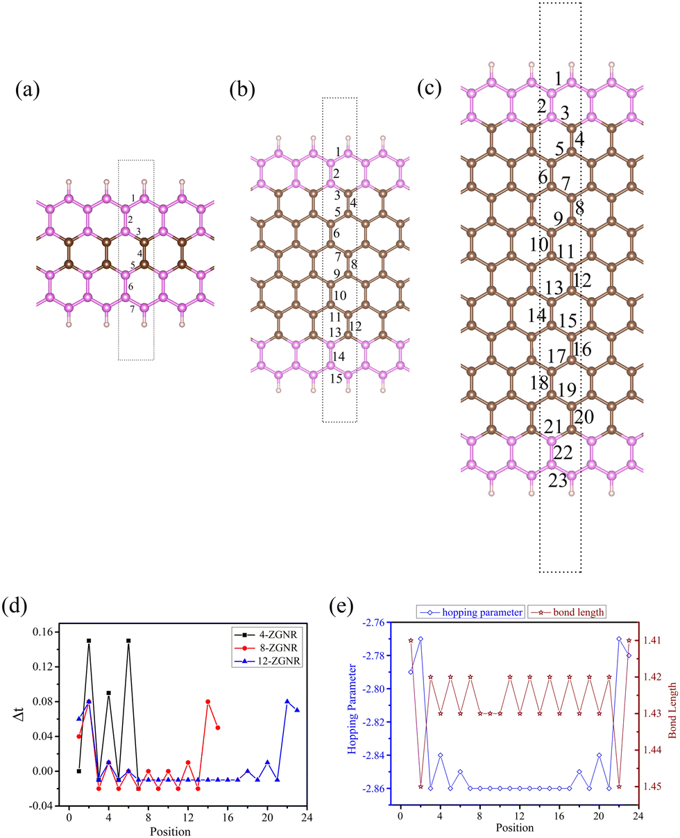
| | Fig. 2 (a)–(c) Relaxed geometries of 8-AGNR, 16-AGNR, and 24-AGNR. Dotted line rectangles refer to the super unit cell of AGNR in the transport channel. (d) and (e) The trend of Δt with the C–C bond index of zig–zag bonds and parallel bonds, respectively. (f) and (g) The value of hopping parameters and bond length with the C–C bond index of zig–zag bonds and parallel bonds of 24-AGNR, respectively. | |
To study the effect of the width of nanoribbons on hopping parameters, we chose AGNRs with widths 8, 16, and 24, as shown in Fig. 3(a)–(c). We defined Δt to evaluate the change of hopping parameters, defined as the following: Δt = tGNR − tgraphene, where, the tGNR is the hopping parameters of the nearest neighbor C atoms of AGNRs, tgraphene is the hopping parameters of the nearest neighbor C atoms of graphene. Firstly, we obtained the hopping parameters of the nearest neighbor C atoms of graphene, tgraphene = −2.85 eV. Each AGNR is divided into two parts, including zig–zag bonds and parallel bonds. From Fig. 3(d), the change of hopping parameters of zig–zag bonds of 8/16/24-AGNR varies from 0 to 0.03 compared with graphene. However, the maximum change of hopping parameters of the parallel bonds of AGNR can reach 0.11, which is larger than that of the zig–zag bonds. The hopping parameters of the internal part are very close to that of graphene. The difference between the hopping parameter of AGNRs at the boundary and the hopping parameter of graphene is 0.11 and 0.08. As the width of AGNR increases, the hopping parameters of the AGNRs are closer to that of graphene, except for the hopping parameters of the C atom at the boundary. Next, we studied the relationship between bond length and hopping parameters. From formula (2), the hopping parameter is related to the distance between two atoms. The relationship between the bond length and hopping parameter of 24-AGNR was plotted in Fig. 3(f) and (g). Due to the boundary effect, the hopping parameters at the edge are significantly different from the internal ones. The internal hopping parameters vary little with bond length, as shown in Fig. 3(f) and (g). The value of hopping parameters and bond length are presented in the ESI.†
 |
| | Fig. 3 (a)–(c) Structures of 4-ZGNR, 8-ZGNR, and 12-ZGNR. Dotted line rectangles refer to the supercell of ZGNR. (d) The trend of Δt with the C–C bond of ZGNRs. (e) The value of hopping parameters and bond length with a C–C bond index of 12-ZGNR. | |
3.2 ZGNRs
Here, for the zigzag edge of graphene nanoribbon, we also constructed three different width structures to study the effect of ZGNR width on hopping parameters, such as 4-ZGNR, 8-ZGNR, and 12-ZGNR. Our calculated results show that the lattice constants of ZGNR are 2.47 Å, which is very close to that reported in the previous literature (2.46 Å).44 The bond length of ZGNRs is similar to that of graphene (1.42 Å). In particular, as the width of ZGNR is wider, the bond length of ZGNR is closer to the bond length of graphene, see Table S2(a)–(c) (ESI†). According to the previous reports, the ground state of ZGNR presents antiferromagnetic (AFM) ordering.47 In Fig. 4, we determined the electronic band structures for (a) 4-ZGNR, (b) 8-ZGNR, and (c) 12-ZGNR, considering the AFM state. This calculation was conducted using the TB method, incorporating precise hopping parameters and employing pz atomic orbitals as projectors. To validate our TB results against density functional theory (DFT) calculations, we included the band structure of 12-ZGNR from DFT in Fig. 4d. Remarkably, the comparison between DFT and TB findings demonstrates a significant agreement, affirming the accuracy of our TB calculations. The formation of gaps in the structure can be attributed to a staggered sublattice potential present in the hexagonal lattice. This potential originates from the edge magnetization within the material. When the atoms along the lattice's edges exhibit distinct magnetic characteristics or orientations compared to those within the interior, it results in an energy disparity or potential between the two sublattices. This energy distinction is responsible for generating band gaps within the material's electronic structure.
 |
| | Fig. 4 The electronic band structures for (a) 4-ZGNR, (b) 8-ZGNR, and (c) 12-ZGNR were computed using the tight-binding method. In panel (d), the band structure of 12-ZGNR was obtained via DFT. | |
Next, we study the hopping parameters between the two nearest neighbor C atoms of ZGNRs and we chose spin-up as a representative to discuss the results of ZGNR. The widths of ZGNRs are 4, 8, and 12, as shown in Fig. 5(a)–(c). The difference between the hopping parameters of ZGNR and those of graphene is plotted in Fig. 5(d). Compared to graphene, the hopping parameter of edge C atoms changes significantly. The variation of hopping parameters of 4-ZGNR can reach up to 0.15 compared to graphene. The change of the hopping parameters of 8/12-ZGNR is smaller than that of 4-ZGNR and the variation of hopping parameters of 8/12-ZGNR is 0.08. However, the hopping parameters of bulk C atoms of 8/12-ZGNR are close to the hopping parameters of graphene. From our calculation results, the edge effect will have a large impact on the hopping parameters of narrow ZGNRs. From Fig. 5(e), we can see that the edge effect has a great impact on the hopping parameters of edge C atoms. Additionally, the value of hopping parameters and bond length of ZGNRs are presented in Table S2 (ESI†). In the following, we use the calculated SD hopping parameters to study the transport properties of GNRs with zig–zag and armchair edges.
 |
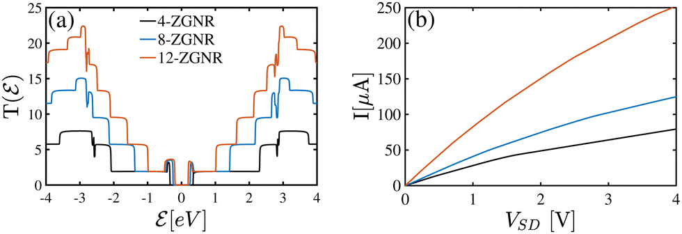
| | Fig. 5 (a) Transmission coefficient and (b) I–V curve of ZGNR with AFM configuration for different ribbon widths. The channel length is constant and equal to 16 carbon atoms. | |
4 Electronic transport
In this section, we will initially examine the electronic transport in ZGNR with an AFM ground state configuration. Following this, we will study the ballistic transport properties of GNR with calculated SD hopping parameters along both armchair and zigzag directions in the absence and presence of an electric field and dilute charged impurities.
4.1 Transport in spin-polarized ZGNR
To investigate the transport properties of the ground state of ZGNR, we conducted quantum transport calculations specifically for the spin-polarized ZGNR, considering its AFM ground state configuration. In Fig. 5, we present the (a) transmission coefficient and the corresponding (b) I–V curve for ZGNRs with AFM configurations across various ribbon widths, while maintaining a constant channel length of 16 carbon atoms. As evident in the transmission spectra, a distinct feature emerges around the Fermi level due to the band gap observed in Fig. 4. This results in a zero transmission probability near the Fermi level for all the ribbon widths under consideration. Notably, a breakdown of mirror electron–hole conduction symmetry is observed in the transmission spectra around the Fermi level for all the considered ribbon widths. With an increase in ribbon width, the transmission probability of ZGNRs remains relatively constant around the Fermi energy but exhibits an upward trend for energy levels far from  . In Fig. 5b, we observe that there is no zero current, which can be attributed to the electron–hole conduction symmetry breaking within the ZGNR structures. Interestingly, wider ZGNRs exhibit higher currents in response to the applied source–drain voltage ([VSD]) when compared to their narrower counterparts. This behavior is a direct result of the improved electron transmission that accompanies the increased ribbon width. Moreover, variations in the width of the ZGNRs can lead to changes in the relative positions of their left and right orbitals, thereby influencing the conductivity of the scattering channel.
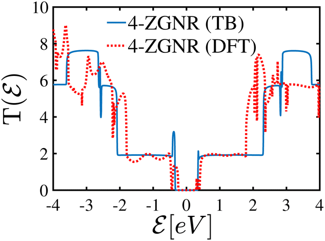
To facilitate a direct comparison between the predictions of the TB model and full DFT transport calculations, we performed electronic transmission coefficient calculations, with a specific focus on the 4-ZGNR configuration characterized by its antiferromagnetic (AFM) order, as illustrated in Fig. 6. Notably, around the Fermi energy, both methods exhibited similar transmission probabilities, indicating good agreement in this crucial region. Also, electron–hole symmetry breaking is observed in both methods. However, as we ventured further from the Fermi levels, deviations between the two approaches became discernible. These disparities can be attributed to a fundamental difference in the way we treated electron interactions in our TB model compared to the comprehensive treatment in DFT. Specifically, our TB model considered only first nearest-neighbor interactions, leading to variations in the transmission spectrum at energy levels further from the Fermi energy.
 |
| | Fig. 6 Comparing the electronic transport of the 4-ZGNR with an AFM configuration, as obtained from both the tight-binding model and full DFT transport calculations. | |
4.2 Comparing transport properties of GNRs with uniform and SD hopping parameters
In this subsection, we conduct a comparative analysis of the transport properties of AGNRs and ZGNRs, considering uniform and SD hopping parameters obtained through the TB and NEGF formalism. To examine the impact of these parameters, we focus on ZGNRs with a ferromagnetic (FM) configuration, given that uniform hopping parameters result in a metallic phase for ZGNRs. We will explore the influence of geometric factors and external perturbations, including the application of a perpendicular electric field and the introduction of dilute charged impurities, on the transport properties of both AGNRs and ZGNRs with uniform and SD hopping parameters.
4.2.1 Geometrical effect.
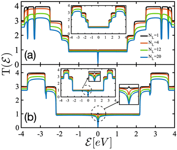
First, we deal with the effects of geometry parameters on the transmission coefficient and current of the system with 2DG and SD hopping parameters. The number of the super unit cells along the length of A(Z)GNR is defined as NL. To compare the effects of SD and 2DG hopping parameters on the electronic properties of GNRs, the DOS of (a) NA-AGNR and (b) NZ-ZGNR for different ribbon widths are illustrated in Fig. 7. In these plots, there are 16 carbon atoms in the channel length and the ribbon width is variable. The solid lines represent the DOS of GNRs with SD hopping parameters and the dotted lines show the DOS of GNRs when the hopping parameters are equal. In the TB model, the electronic phase of NA-AGNR with 2DG hopping parameters depends on the width of the ribbon NA, whereas NZ-ZGNRs is metal for the whole range of the ribbon width. As explained, NA-AGNRs have been classified into three separate categories. They behave as metal when the ribbon width is NA = 3p + 2 (p is a positive integer number,  ) and they show semiconductor behavior when NA = 3p and NA = 3p + 1.19,48–51 However, as shown in Fig. 1, there is a gap in the band structure of AGNRs obtained from DFT calculations for all three considered widths. Consequently, in first-principles calculations, AGNRs are semiconductors independent of their width. These band gaps for AGNRs are due to quantum confinement and deformation due to edge dangling bonds.21,52 By this, NA = 8 = 3 × p + 2 with p = 2 which corresponds to the metallic AGNR with the 2DG hopping value which is also observed in Fig. 7(a). On the contrary, the DOS of 8-AGNR with SD hopping parameters shows a dip at the Fermi level. Comparison between the DOS of A(Z)GNR with SD and 2DG hopping parameters reveals some extra dips at energies far from
  for GNR with SD hopping energies. The number of these extra degenerate states goes up by increasing the ribbon width. Moreover, the metallic phase of NZ-ZGNR is found for all considered widths in panel (b). Sharp peaks at the Fermi energy level in the DOS of NZ-ZGNRs are observed due to the flat bands coming from the edge states. These states are related to the wavenumber k. An increase in the ribbon width leads to a shift in degenerate states to lower (higher) energy levels for the bands in the conduction (valence) region. For 4-ZGNR with SD hopping parameters, the distance of degenerate states at the valence and conduction band from the Fermi level is less than 4-ZGNR with the 2DG hopping parameter, while for the case of 8/12-ZGNR, no significant change is found in the location of the degenerate state by changing the values of the hopping parameter. Furthermore, for NZ-ZGNRs with SD hopping parameters, an electron–hole symmetry breaking is observed in the distribution of the states at energy levels around ±2.8 eV corresponding to the mid-region between two edges. However, there is a mirror symmetry between the conduction and valence bands for ZGNR with the uniform ts. Now, we deal with the electronic transmission probability of NA(Z)-A(Z)GNRs as a function of energy when the ribbon length is constant and equal to 16 C atoms, and the width of the ribbon changes. Fig. 8 compares the transmission coefficient of (a) NA-AGNR and (b) NZ-ZGNR for different widths. The inset panels show the results of GNRs with equivalent hopping parameters. The findings indicate that by increasing the ribbon width the transmission probability of A(Z)GNRs also rises. Transmission probability is the number of available subbands at a given energy level. The transmission spectrum shows step-like behavior that is related to existing conduction channels. A dip appears in the transmission probability of 8-AGNR with SD t at the Fermi level in panel (a). However, for 8-AGNR with 2DG hopping parameters,
  is non-zero and remains constant around the Fermi energy. Thus, the dip at
  is associated with the semiconductor nature of NA-AGNR in the first-principles calculations. Some extra dips are observed in the electronic transmission of A(Z)GNR for all considered widths when hopping parameters are realistic which is related to the reduction of the DOS at the corresponding energy levels in Fig. 7. The appearance of sharp dips means that the number of conducting channels alters at related energy levels. For AGNRs in panel (a), mirror symmetry is observed in transmission spectra between the valence and conduction bands in all considered widths while for 4-ZGNRs with SD t, the mirror electron–hole conduction symmetry breaks down at energy levels equal to ±2.7 eV, because unbalanced carriers are injected from metal electrodes. The different behavior of the transmission spectrum of AGNRs and ZGNRs comes from the absence of valley mixing at the edge of the zig–zag nanoribbons. In ZGNRs, the forward propagating mode belongs to the K valley whereas the backward propagating mode comes from the K′ valley. As a result, valley mixing stops due to the presence of edge states. Electron back-scattering requires mixing of K and K′ valleys which happens in AGNRs. Panel (b) shows the non-zero value of
  in the zig–zag direction, which confirms the metallic phase of the system. As the ribbon width increases, the transmission probability of A(Z)GNRs remains constant around the Fermi energy and it goes up for energy levels far from
  . The number of steps for all considered systems is also enhanced by increasing the ribbon width. This is due to the presence of more atoms in the super unit cell of wider A(Z)GNRs and hence, more electrons tunneling across the energy barrier giving rise to constructive interference and more transmission channels. The fluctuations in electronic transport observed in graphene ribbon structures align with the conclusions of ref. 53 and 54. The experimental research underscores the importance of considering ribbon dimensions and orientations as influential factors in shaping the electrical properties of graphene structures.53 This understanding marks an essential early step in the development of graphene-based electronic devices.
 |
| | Fig. 7 DOS of (a) AGNR and (b) ZGNR with 2DG and SD hopping parameters for different ribbon widths. The channel length is constant and equal to 16 carbon atoms. | |
 |
| | Fig. 8 Transmission spectrum of (a) NA-AGNR and (b) NZ-ZGNR with 2DG and SD hopping parameters for different ribbon widths. The channel length is constant and equal to 16 carbon atoms. | |
To study the transport properties of A(Z)GNRs under source–drain potential (VSD), we have plotted the current–voltage (I–V) curves of NA-AGNRs and (b) NZ-ZGNRs with different width sizes in Fig. 9. The results indicate that the current of A(Z)GNRs with 2DG and SD hopping parameters behave similarly for each specified width. In panel (a), the current of the AGNRs is zero at the low source–drain voltage range corresponding to the band gap of the system. This zero-current region for 8-AGNRs is less than two other ones. By increasing the source–drain potential, the current of the system goes up and shows non-zero values indicating that new channels are opened. From panel (b), no zero-current is observed which confirmed the metallic phase of NZ-ZGNRs with the 2DG and SD hopping parameters. Moreover, the I–V curves of ZGNRs show similar behavior for a lower source–drain potential. However, there is a significant augmentation of current at a higher source–drain voltage for wider ZGNRs [VSD ≳ 2.8 eV for 8-ZGNR and VSD ≳ 2 eV for 12-ZGNR]. Therefore, for 8- and 12-ZGNRs linear-to-nonlinear ohmic transitions occur at the higher strength of source–drain potential. Whereas 16- and 24-AGNRs behave as a non-Ohmic device in the whole range of VSD. Wider ribbons of A(Z)GNRs show more current at higher values of VSD compared to narrow ones due to the improved electron transmission by increasing the ribbon width. Furthermore, changes in the width of A(Z)GNRs can move the relative position of their left and right orbitals which leads to adjusting the conductivity of the scattering channel (Fig. 9).
 |
| | Fig. 9
I–V characteristics of (a) NA-AGNRs and (b) NZ-ZGNRs with 2DG and SD hopping parameters. The channel length is constant and equal to 16 carbon atoms while the number of atoms in the width of the ribbon is variable. | |
To understand the effects of increasing central channel length, we have calculated the energy-dependent transmission coefficient of (a) 8-AGNR and (b) 4-ZGNR for different channel lengths NL = 1, 4, 12, and 20 super unit cells of NA(Z)-A(Z)GNRs, as illustrated in Fig. 10. Results show that transmission probabilities of both considered systems with the 2DG and SD hopping parameters decrease by increasing the ribbon length along both zig–zag and armchair directions. Besides, there is no significant change in the step-like behavior and degeneracy of energy levels in  for different scattering channel lengths. These results are in good agreement with ref. 55. Furthermore, from panel (b) we can see an increase in the conductance of 4-ZGNR when there is only one super unit cell in the central channel. This could be due to the overlap between electrodes. However, for longer scattering channels, the transmission probability declines around the zero-energy which shows that for narrow 4-ZGNRs, the two valleys in the band structure are not well separated in momentum space and the flat bands have a limited curvature. Thus, if one considers a sufficient wider ribbon, the transmission probability will completely recover at the Fermi level.26
 |
| | Fig. 10 Transmission coefficient of (a) 8-AGNR and (b) 4-ZGNR with SD hopping parameters for different ribbon lengths. NL is the number of 8(4)-A(Z)GNR super unit cells in the scattering channel. The inset panel presents the  of GNRs with 2DG hopping parameters. of GNRs with 2DG hopping parameters. | |
The I–V curves for NL = 1, 4, 12, and 20 super unit cells of (a) 8-AGNRs and (b) 4-ZGNR are presented in Fig. 11, respectively. In the insets, the I–V characteristics of (a) 8-AGNR and (b) 4-ZGNR with 2DG hopping parameters are presented. In panel (a), both the 8-AGNR systems, one with equivalent hopping parameters (inset panel) and the other with realistic hopping parameters, exhibit a non-zero current when a bias voltage is applied. Furthermore, the current of all considered systems is reduced by increasing the length of the central channel. The reason for this current drop is the scattering of electrons among those states belonging to continuous bands due to the smooth variation of the VSD along the ribbon. Therefore, the blockage caused by electronic transmission between the disconnected bands intensifies with increasing the scattering channel length. Changing the current and transmission coefficient of GNRs depending on their geometrical parameters allows us to tune their transport characteristics to obtain high-performance switches. From now on, we only focus on the transport properties of 8-AGNR and 4-ZGNR with 16 C atoms in the scattering channel length.
 |
| | Fig. 11
I–V characteristics of (a) 8-AGNR and (b) 4-ZGNR with SD hopping parameters for different ribbon lengths. The inset panel presents the  of GNRs with 2DG hopping parameters. of GNRs with 2DG hopping parameters. | |
4.2.2 Perpendicular electric field effect.
Application of a perpendicular electric field (PEF) is a common route in engineering the electronic transport properties of the systems at the nanoscale and makes them suitable for applications in semiconductor devices. A simple way to apply PEF to a nanoribbon is installing the gate voltage on the top and bottom of its ribbons. In the present section, we investigate the transport property of GNRs in the presence of PEF using a rather simple but explicit tight-binding model| |  | (8) |
where Vi is the gate voltage.
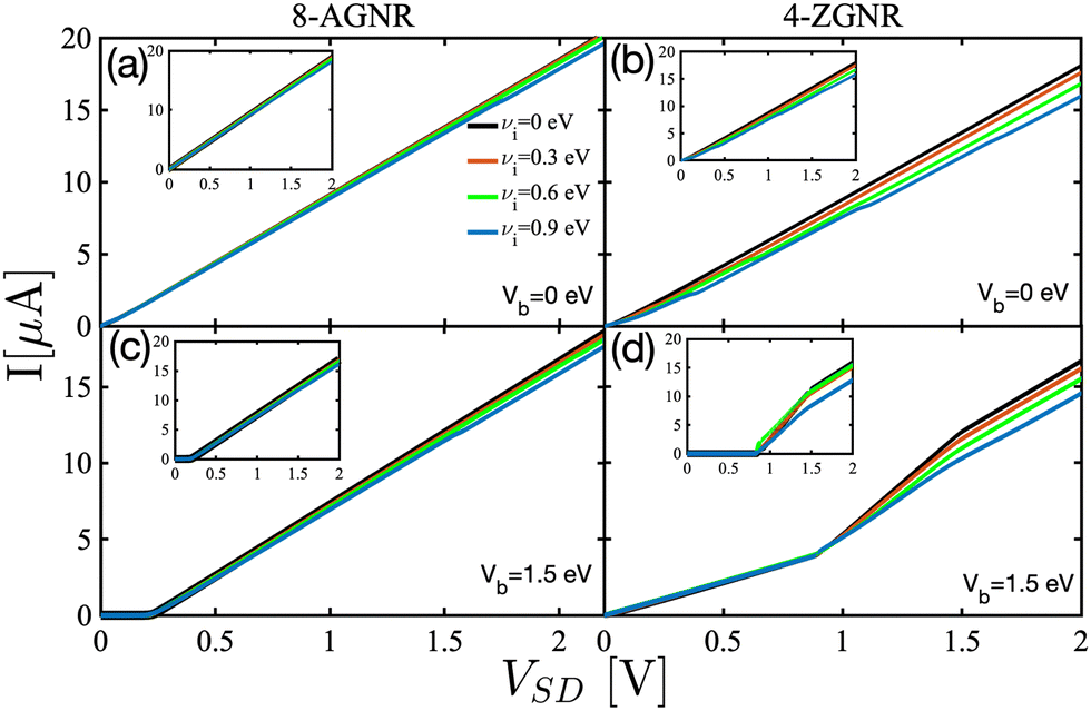
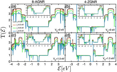
Using the above perturbed Hamiltonian (eqn (8)), we have calculated the effects of voltage biasing on the electronic transmission and I–V characteristic of A(Z)GNR which are illustrated in Fig. 12 and 14, respectively. Applying an external PEF on the nanoribbons can create a shift in the energy dispersion and Fermi energy leading to inducing a band gap and metal-to-semiconductor phase transition. Such phase transitions in EF-induced ZGNRs are also reported in ref. 56–59. As shown in Fig. 12(a), a zero-transmission probability emerges around the Fermi level in the transmission spectra of 8-AGNR with and without 2DG hopping parameters under the application of PEF. This zero-transmission region increases by increasing the strength of the PEF. For all considered systems, some shifts in the transmission channels are observed in the presence of PEF because applying PEF results in moving in the bands at the valence and conduction region. In the insets, the transmission probability of (a) 8-AGNR and (b) 4-ZGNR with the same hopping parameters are illustrated and symmetry behavior can be seen. In panel (b), for electric field-induced 4-ZGNR with SD hopping energy, electron–hole asymmetry leads to the appearance of zero transmission probability only at the energy levels higher than  . Similar to 8-AGNR, an increase in the strength of the applied PEF boosts the zero-transmission region of 4-ZGNR. Electric field-induced 4-ZGNR with an SD hopping parameter shows a strong electron–hole symmetry breaking in the inter-valley scattering of holes and electrons and therefore the transport properties. Interestingly, we found that electric field-induced 4-ZGNR with SD hopping parameters suffers from a metal-to-n-doped semiconductor phase transition because of the electron–hole asymmetry in this material. Thus, it is expected that if one changes the sign of the applied PEF, i.e. through application of a negative bias voltage, a metal-to-p-doped semiconductor phase transition will emerge in 4-ZGNR with realistic hopping parameters. To support this statement we have plotted the electronic band structure and DOS of 4-ZGNR with SD hopping parameters under the application of (a) Vb = +2.5 eV and (b) Vb = −2.5 eV shown in Fig. 13. As illustrated in the figure, the application of PEF makes a shift in the degeneracy of the flat bands at the Fermi level, and consequently, band gap opening is observed. From panel (a) it is clear that for the case of applying a positive electric field, there is a band gap from 0 to 0.62 eV in the conduction band, while the energy gap appears at −0.62 to 0 eV in the presence of negative PEF [panel (b)].
 |
| | Fig. 12 Effects of the PEF on the energy-dependent transmission coefficient of (a) 8-AGNR and (b) 4-ZGNR with SD hopping parameters for the case that there are 16 carbon atoms in the scattering channel. The inset panel presents the transmission probability of GNRs with 2DG hopping parameters. | |
 |
| | Fig. 13 Electronic band structure and DOS of 4-ZGNR with realistic hopping parameters in the presence of PEF (a) Vb = +2.5 eV and (b) Vb = −2.5 eV. Dashed lines refer to the Fermi level. | |
The effect of applying PEF on the current of the (a) 8-AGNR and (b) 4-ZGNR is presented in Fig. 14. As shown in panel (a), no current passes through the system at a low source–drain voltage due to the opening of a band gap in PEF induced-AGNRs. The zero-current range goes up for stronger PEF. Panel (b) compares the influences of the presence of PEF on 4-ZGNRs with 2DG (inset panel) and SD hopping energies. It is seen that the biased 4-ZGNR with the 2DG hopping parameters behaves as a non-ohmic device and no current is found at low source–drain potential. The zero-current range boosts by increasing the strength of the external field so that no current is observed up to VSD = 1.2 eV when Vb = 2.5 eV. However, for the biased 4-ZGNR with SD hopping parameters, the current starts flowing once the source–drain potential is applied and a linear-to-nonlinear ohmic transition is observed for 4-ZGNR with SD t in the presence of PEF. This difference in the I–V characteristic curves of 4-ZGNR with 2DG and SD hopping parameters originates from the (a) symmetry of the systems which directly affects the coupling between the wave functions of the π and π* sub-bands around the Fermi energy. In ref. 60, in biased NZ-ZGNRs, an electron–hole asymmetry and ohmic current–voltage are observed only if the width of the ribbon (NZ) is odd. Moreover, for the case of even NZ, a mirror-symmetry in the electronic transport properties of electric field-induced NZ-ZGNR is reported and the current of the biased system behaves similarly to the one with 2DG hopping parameters due to the existence of a conductance gap around the Fermi energy. Interestingly, here we found that mirror asymmetry of the ZGNRs under bias voltage is independent of the ribbon width when hopping parameters are realistic. Thus, biased ZGNR with SD hopping parameters behaves like an ohmic conductor, although the width of the ribbon is even. Furthermore, the current of all considered devices is reduced by increasing the strength of the applied PEF. Thus, applying the PEF can modulate the electronic transport properties of GNRs. The experimental literature has provided compelling evidence that the transport characteristics of GNRs can be modulated in the presence of an electric field.61 In situations where transport is primarily governed by hopping through localized states, the applied electric field effectively assumes the role of temperature. Consequently, the electric field can be treated as an effective temperature, denoted as kBTeff = eELc, where Lc represents the characteristic hopping length between localized states.61,62
 |
| | Fig. 14 Current–voltage characteristic of biased (a) 8-AGNR and (b) 4-ZGNR with SD hopping parameters for the case that there are 16 carbon atoms in the scattering channel. The inset panel presents the transmission probability of GNRs with 2DG hopping parameters. | |
4.2.3 Electron-impurity interaction effects.
In this subsection, we are looking to elucidate the electronic transport of GNRs with armchair and zig–zag edges in the presence of dilute charged impurity. We used the Born approximation in the calculations of short-range impurity.63 In our calculations, the impurities are stochastically doped into the system. Thus, we only focus on the concentration of impurities ni and the scattering potential νi induced to the transport channel. Impurity concentration is defined as the ratio of the number of impurity atoms Ni to the number of unit cells. Using the tight-binding model the contact interaction between the electrons of the GNR lattice and external impurities can be written as| |  | (9) |
in which stands for unit cell atoms and  implies induced momenta by impurities belonging to the FBZ.
With the aid of the interaction picture and the Matsubara Green's function,63,64 it is possible to write the interacting Green's function of the system as
| |  | (10) |
in which
τ refers to the imaginary time and
U(
β,0) is the time evolution operator (
β = 1/
kBT), given by
| |  | (11) |
In the Born approximation framework, the electronic self-energy image

of the disordered system is a state-independent constant for electron-impurity interaction
| |  | (12) |
where
Nuc is the number of unit cells. Using the Dyson equation the perturbative configuration for the Green's function of the disordered system can be obtained as:
63| |  | (13) |
Now, the Green's function of the dilute charged impurity-induced scattering channel can be calculated by substituting the Green's function of the scattering channel in
eqn (3) into
eqn (13). Moreover, the

of the system in the presence of charged dilute impurity can be computed by substituting the perturbed Green's function in
eqn (13) into
eqn (6). Eventually, substituting the calculated

of the perturbed system into the Landauer–Büttiker formula,
eqn (7), gives the currents of the impurity-imbrued system as a function of the voltage.
Here, we study the electronic transport properties of GNRs in the presence of dilute impurities in two cases. First, we consider different impurity concentrations while νi is constant. A different ni means that we address the same impurities characterized using a fixed scattering potential. Next, we focus on the impurity-induced system with different νi at fixed ni, which means that we deal with different impurities characterized by a fixed impurity concentration.
First, for a better understanding of charged impurity effects on the transmission coefficient, we calculated the perturbed DOS of impurity-induced (a) 8-AGNRs and (b) 4-ZGNRs in Fig. 15 under the condition that the scattering potential and impurity concentration are fixed at 0.5 eV and ni = 10%, respectively. As illustrated, the height of van Hove singularities reduces in the presence of the charged impurity. Moreover, some extra degenerate states appear at perturbed DOS curves. As a result, the electron–hole symmetry breaks down which can improve the application of GNR devices. A comparison between the results of 8-AGNR with SD hopping parameters and the other one with uniform t in the inset panel (a) shows that the DOS of AGNR with SD hopping has a non-zero value at the Fermi level in the presence of charged impurity.
 |
| | Fig. 15 DOS of pristine and impurity-induced (a) 8-AGNR and (b) 4-ZGNR with SD hopping parameters. The scattering potential and impurity concentration are fixed at 0.5 eV and ni = 10%, respectively. There are 16 carbon atoms in the scattering channel. The inset panel presents the current of GNRs with equivalent hopping parameters. | |
Now, let's address the effects of charged impurities on the electronic transmission spectrum of 8-AGNR (left panels) and 4-ZGNR (right panels) which are presented in Fig. 16. The impurity scattering potential is fixed at νi = 0.5 eV. We found that for both (a) 8-AGNRs and (b) 4-ZGNRs with 2DG and SD hopping energies, the step-like behavior of the transmission coefficient of pristine and doped GNRs are similar, but for the energy level far from the Fermi energy, a sharp spike appears. Also, charged impurities lead to a reduction in their transmission probability especially at the energy levels farther from  . Moreover, it is found that no extra zero transmission channels are observed in the transmission spectra of GNRs subjected to dilute charged impurities. Besides, extra dips are found in the zero-bias transmission spectra of 4-ZGNRs around the Fermi level in panel (b) which results from the strong localization of electronic states in these systems. For further study, we carried out the above calculations for the case in which the dilute charged impurity and bias potential are applied to the system simultaneously which are shown in panels (c) and (d). Again, the interaction between impurity atoms and the charge carriers in GNR makes a depopulation of the sub-bands, and consequently
  decreases by increasing the impurity concentration. Moreover, electron–hole symmetry breaking is found in the transmission spectra of all considered systems in the presence of electron-impurity interaction effects which is directly related to the appearance of the electron–hole asymmetry in their band structure. As demonstrated in the lower panels (c) and (d), the application of PEF enhances the electron–hole asymmetry of impurity-induced GNRs, thus more extra dips are observed. Our findings are in good agreement with ref. 65 in which such decrements in transmission coefficient of impurity-doped GNRs with zig–zag edges have been observed.
 |
| | Fig. 16 Energy dependent transmission of impurity-induced (a) and (c) 8-AGNR and (b) and (d) 4-ZGNR with SD hopping parameters in the absence (panels a and b) and presence of PEF (panels c and d). There are 16 carbon atoms in the scattering channel. The inset panel presents the transmission probability of GNRs with 2DG hopping parameters. The scattering potential is fixed at 0.5 eV. | |
In Fig. 17, the results for the current as a function of the applied source–drain voltage for (a, c) 8-AGNR and (b) and (d) 4-ZGNR in the presence of charged dilute impurity are illustrated. Inset panels present the I–V plots for impurity-induced (a, c) 8-AGNR and (b) and (d) 4-ZGNR with equivalent t. The upper and lower panels show the plots for zero-biased and biased A(Z)GNRs, respectively. Again, the impurity scattering potential is set to 0.5 eV. No additional zero current region is observed for the charged impurity-induced (a) 8-AGNRs and (b) 4-ZGNRs in the absence of PEF. Also, for (a) zero-bias and (c) biased 8-AGNRs with and without realistic hopping parameters no significant change is found by adding charged dilute impurities, while for 4-ZGNRs (panels b and d) charged impurities make a decrease in the current at a higher source–drain potential.
 |
| | Fig. 17
I–V characteristic of the impurity-induced (a) and (c) 8-AGNR and (b) and (d) 4-ZGNR with SD hopping parameters in the absence (panels a and b) and presence of PEF (panels c and d). There are 16 carbon atoms in the scattering channel. The inset panel presents the current of GNRs with the same hopping parameters. The scattering potential is fixed at 0.5 eV. | |
Now, we deal with the transport properties of charged impurity-induced A(Z)GNRs in the case that the impurity scattering potential increases at a fixed impurity concentration. Fig. 18 exhibits the same as Fig. 16, but for different values of scattering potential. The impurity concentration is set to ni = 10%. Similar to previous figures, insets compare the same results for 8-GNRs with equivalent t. As illustrated in panels (a) and (b), it is clear that by increasing the scattering potential the electronic transmission probability of zero-biased GNRs with and without equivalent hopping parameters reduces. Also, additional spike sharps appear in the transmission spectra in the presence of impurities. For biased (c) 8-AGNR and (d) 4-ZGNR more oscillations are found in the transmission spectrum. Besides, the step-like behavior of  disappears especially at energy levels far from
  for stronger scattering potentials. A comparison between Fig. 16 and 18 reveals that the strength of scattering potential plays a more effective role than the impurity concentration in controlling the transport properties of GNRs.
 |
| | Fig. 18 Transmission coefficients as a function of energy for impurity-induced (a) and (c) 8-AGNR and (b) and (d) 4-ZGNR with SD hopping parameters. Results for unbiased and biased GNRs are presented in panels (a) and (b) and (c) and (d), respectively. There are 16 carbon atoms in the scattering channel. The inset panel presents the transmission probability of GNRs with the same hopping parameters. The impurity concentration ni = 10% was fixed for the plots. | |
Fig. 19 presents the same as in the upper and lower panels of Fig. 17, but in this case, the impurity scattering potential increases when the impurity concentration is fixed at 10%. I–V plots have almost similar behavior in the absence and presence of dilute charged impurity. However, for higher values of source–drain potential, the currents of impurity-imbrued GNRs decrease with respect to the pristine ones. The plots indicate that the effects of adding dilute charged impurities on the I–V characteristic of 4-ZGNRs is more than armchair ones which are true for both biased and unbiased systems.
 |
| | Fig. 19
I–V characteristics for impurity-induced (a) and (c) 8-AGNR and (b) and (d) 4-ZGNR with SD hopping parameters. Results for unbiased and biased GNRs are presented in panels (a) and (b) and (c) and (d), respectively. There are 16 carbon atoms in the scattering channel. The inset panel presents the transmission probability of GNRs with the same hopping parameters. The impurity concentration ni = 10% was fixed for the plots. | |
5 Conclusions
Based on DFT calculations and the construction of maximally localized Wannier functions, we provide values of hopping parameters of AGNRs and ZGNRs with different widths. The edge effect has a significant influence on the hopping parameters of narrow A(Z)GNRs. Our results show that the hopping parameters of the edge atoms and bulk atoms of narrow A(Z)GNRs vary, compared with that of graphene. However, only the hopping parameter of edge atoms changes for the wide A(Z)GNRs. Compared to graphene, the change of hopping parameter of edge C atoms of ZGNRs and AGNRs is as high as 0.11 and 0.08, respectively, and the hopping parameter of bulk atoms is similar to that of graphene. Therefore, it is unreasonable to use 2DG hopping parameters in the TB model of A(Z)GNRs.
Furthermore, electronic transport properties of GNRs with the obtained realistic hopping parameters have been studied using the Green's function approach and the Landauer–Büttiker formalism. Effects of application of a perpendicular electric field and dilute charged impurities are also studied based on self-consistent Born approximation. It is found that the electron–hole symmetry breaks down in ZGNRs with SD hopping parameters. Besides, the electronic phase of AGNRs with 2DG hopping energies depends on their width, whereas there is a band gap in the electronic structure of AGNRs with 2DG hopping parameters for all widths. Moreover, the results indicated that the effect of increasing ribbon width on modulating the transport properties of GNRs is more than increasing the channel length. In addition, we show that the transport properties of A(Z)GNRs can be controlled in the presence of an electric field and charged impurities. Interestingly, a metal-to-n(p)-doped semiconductor phase transition is observed in the electronic structure of 4-ZGNR with realistic hopping parameters in the presence of positive (negative) external bias voltage. Applying an electric field on 4-ZGNR with 2DG hopping parameters leads to opening a band gap in both the conduction and valence bands. We also found an electron–hole asymmetry in the dilute charged impurity-induced GNRs. Furthermore, the transmission probability and current of the system decreased in the presence of charged impurities and external perpendicular electric fields.
Author contributions
M. Davoudiniya: methodology, data curation, visualization, analysis, writing of paper. B. Yang: methodology, data curation, visualization, analysis, writing of paper. B. Sanyal: conceptualization, funding acquisition, supervision, analysis of results, writing of paper.
Conflicts of interest
The authors declare no competing financial interest.
Acknowledgements
B. S. acknowledges financial support from Swedish Research Council (grant no. 2022-04309). B. Y. acknowledges funding from National Natural Science Foundation of China (grant no. 12104258). The computations were enabled by resources provided by the National Academic Infrastructure for Supercomputing in Sweden (NAISS) at UPPMAX (NAISS 2023/5-238) and the Swedish National Infrastructure for Computing (SNIC) (SNIC 2022/3-30) at NSC and PDC partially funded by the Swedish Research Council through grant agreements no. 2022-06725 and no. 2018-05973. B. S. also acknowledges the allocation of supercomputing hours in EuroHPC resources in Karolina supercomputer in the Czech Republic.
References
- K. S. Novoselov, A. K. Geim, S. V. Morozov, D. Jiang, Y. Zhang, S. V. Dubonos, I. V. Grigorieva and A. A. Firsov, Science, 2004, 306, 666–669 CrossRef CAS PubMed.
- P. Avouris and C. Dimitrakopoulos, Mater. today, 2012, 15, 86–97 CrossRef CAS.
- K. S. Novoselov, A. K. Geim, S. Morozov, D. Jiang, M. Katsnelson, I. Grigorieva, S. Dubonos and A. A. Firsov, Nature, 2005, 438, 197 CrossRef CAS PubMed.
-
M. S. Dresselhaus, G. Dresselhaus and P. C. Eklund, Science of fullerenes and carbon nanotubes: their properties and applications, Elsevier, 1996 Search PubMed.
- A. Celis, M. Nair, A. Taleb-Ibrahimi, E. Conrad, C. Berger, W. De Heer and A. Tejeda, J. Phys. D: Appl. Phys., 2016, 49, 143001 CrossRef.
- K. Wakabayashi, K.-I. Sasaki, T. Nakanishi and T. Enoki, Sci. Technol. Adv. Mater., 2010, 11, 054504 CrossRef PubMed.
- M. Terrones, A. R. Botello-Méndez, J. Campos-Delgado, F. López-Uras, Y. I. Vega-Cantú, F. J. Rodrguez-Macas, A. L. Elas, E. Munoz-Sandoval, A. G. Cano-Márquez and J.-C. Charlier,
et al.
, Nano Today, 2010, 5, 351–372 CrossRef.
- M. F. De Volder, S. H. Tawfick, R. H. Baughman and A. J. Hart, Science, 2013, 339, 535–539 CrossRef CAS PubMed.
- A. Eatemadi, H. Daraee, H. Karimkhanloo, M. Kouhi, N. Zarghami, A. Akbarzadeh, M. Abasi, Y. Hanifehpour and S. W. Joo, Nanoscale Res. Lett., 2014, 9, 393 CrossRef PubMed.
- Y. Zhang, Y.-W. Tan, H. L. Stormer and P. Kim, Nature, 2005, 438, 201 CrossRef CAS PubMed.
- H. Hiura, Appl. Surf. Sci., 2004, 222, 374–381 CrossRef CAS.
- L. Cançado, M. Pimenta, B. Neves, G. Medeiros-Ribeiro, T. Enoki, Y. Kobayashi, K. Takai, K.-I. Fukui, M. Dresselhaus and R. Saito,
et al.
, Phys. Rev. Lett., 2004, 93, 047403 CrossRef PubMed.
- K. Wakabayashi, Phys. Rev. B: Condens. Matter Mater. Phys., 2001, 64, 125428 CrossRef.
- B. Huang, Z. Li, Z. Liu, G. Zhou, S. Hao, J. Wu, B.-L. Gu and W. Duan, J. Phys. Chem. C, 2008, 112, 13442–13446 CrossRef CAS.
- E.-j Kan, Z. Li, J. Yang and J. Hou, J. Am. Chem. Soc., 2008, 130, 4224–4225 CrossRef CAS PubMed.
- C. Xu, C. Wang, C. T. Chan and K. Ho, J. Phys.: Condens. Matter, 1992, 4, 6047 CrossRef CAS.
- D. Bahamon, A. Pereira and P. Schulz, Phys. Rev. B: Condens. Matter Mater. Phys., 2011, 83, 155436 CrossRef.
- R. Grassi, S. Poli, E. Gnani, A. Gnudi, S. Reggiani and G. Baccarani, Solid-State Electron., 2009, 53, 462–467 CrossRef CAS.
- L. Brey and H. Fertig, Phys. Rev. B: Condens. Matter Mater. Phys., 2006, 73, 235411 CrossRef.
- K. Nakada, M. Fujita, G. Dresselhaus and M. S. Dresselhaus, Phys. Rev. B: Condens. Matter Mater. Phys., 1996, 54, 17954 CrossRef CAS PubMed.
- Y.-W. Son, M. L. Cohen and S. G. Louie, Phys. Rev. Lett., 2006, 97, 216803 CrossRef PubMed.
- K. Wakabayashi, M. Fujita, H. Ajiki and M. Sigrist, Phys. Rev. B: Condens. Matter Mater. Phys., 1999, 59, 8271 CrossRef CAS.
- K. Wakabayashi, M. Sigrist and M. Fujita, J. Phys. Soc. Jpn., 1998, 67, 2089–2093 CrossRef CAS.
- Y.-W. Son, M. L. Cohen and S. G. Louie, Nature, 2006, 444, 347 CrossRef CAS PubMed.
- K. Wakabayashi, Y. Takane, M. Yamamoto and M. Sigrist, New J. Phys., 2009, 11, 095016 CrossRef.
- K. Wakabayashi, Y. Takane, M. Yamamoto and M. Sigrist, Carbon, 2009, 47, 124–137 CrossRef CAS.
- V.-T. Tran, J. Saint-Martin and P. Dollfus, Phys. Rev. B, 2020, 102, 075425 CrossRef CAS.
- A. Ahmadi Fouladi and S. Ketabi, Phys. E, 2015, 74, 475–480 CrossRef CAS.
- B. Ghosh, S. Nahas, S. Bhowmick and A. Agarwal, Phys. Rev. B: Condens. Matter Mater. Phys., 2015, 91, 115433 CrossRef.
- P. Lazić, K. D. Belashchenko and I. Z. Žutić, Phys. Rev. B, 2016, 93, 241401 CrossRef.
- C.-H. Wu, Results Phys., 2018, 11, 1182–1191 CrossRef.
- G. Kresse and J. Hafner, Phys. Rev. B: Condens. Matter Mater. Phys., 1993, 48, 13115 CrossRef CAS PubMed.
- G. Kresse and J. Furthmüller, Phys. Rev. B: Condens. Matter Mater. Phys., 1996, 54, 11169 CrossRef CAS PubMed.
- G. Kresse and D. Joubert, Phys. Rev. B: Condens. Matter Mater. Phys., 1999, 59, 1758 CrossRef CAS.
- P. E. Blöchl, Phys. Rev. B: Condens. Matter Mater. Phys., 1994, 50, 17953 CrossRef PubMed.
- J. P. Perdew, K. Burke and M. Ernzerhof, Phys. Rev. Lett., 1996, 77, 3865 CrossRef CAS PubMed.
- H. J. Monkhorst and J. D. Pack, Phys. Rev. B: Condens. Matter Mater. Phys., 1976, 13, 5188 CrossRef.
- N. Marzari and D. Vanderbilt, Phys. Rev. B: Condens. Matter Mater. Phys., 1997, 56, 12847 CrossRef CAS.
- A. A. Mostofi, J. R. Yates, Y.-S. Lee, I. Souza, D. Vanderbilt and N. Marzari, Comput. Phys. Commun., 2008, 178, 685–699 CrossRef CAS.
- S. Smidstrup, T. Markussen, P. Vancraeyveld, J. Wellendorff, J. Schneider, T. Gunst, B. Verstichel, D. Stradi, P. A. Khomyakov, U. G. Vej-Hansen, M.-E. Lee, S. T. Chill, F. Rasmussen, G. Penazzi, F. Corsetti, A. Ojanperä, K. Jensen, M. L. N. Palsgaard, U. Martinez, A. Blom, M. Brandbyge and K. Stokbro, J. Phys.: Condens. Matter, 2019, 32, 015901 CrossRef PubMed.
- M. P. L. Sancho, J. M. L. Sancho, J. M. L. Sancho and J. Rubio, J. Phys. F: Met. Phys., 1985, 15, 851–858 CrossRef.
- D. H. Lee and J. D. Joannopoulos, Phys. Rev. B: Condens. Matter Mater. Phys., 1981, 23, 4997–5004 CrossRef.
-
S. Datta, Quantum Transport: Atom to Transistor, Cambridge University Press, 2005 Search PubMed.
- R. Rasuli and H. Rafii-Tabar,
et al.
, Phys. Rev. B: Condens. Matter Mater. Phys., 2010, 81, 125409 CrossRef.
- X. Gao and X. Shen, Carbon, 2017, 125, 536–543 CrossRef CAS.
- K. Wakabayashi, M. Fujita, H. Ajiki and M. Sigrist, Phys. Rev. B: Condens. Matter Mater. Phys., 1999, 59, 8271 CrossRef CAS.
- G. Cantele, Y.-S. Lee, D. Ninno and N. Marzari, Nano Lett., 2009, 9, 3425–3429 CrossRef CAS PubMed.
- B. Sahu, H. Min, A. H. MacDonald and S. K. Banerjee, Phys. Rev. B: Condens. Matter Mater. Phys., 2008, 78, 045404 CrossRef.
- M. Ezawa, Phys. Rev. B: Condens. Matter Mater. Phys., 2006, 73, 045432 CrossRef.
- Y. Hancock, A. Uppstu, K. Saloriutta, A. Harju and M. J. Puska, Phys. Rev. B: Condens. Matter Mater. Phys., 2010, 81, 245402 CrossRef.
- K. Wakabayashi, M. Fujita, H. Ajiki and M. Sigrist, Phys. Rev. B: Condens. Matter Mater. Phys., 1999, 59, 8271–8282 CrossRef CAS.
- A. V. Rozhkov, S. Savel'ev and F. Nori, Phys. Rev. B: Condens. Matter Mater. Phys., 2009, 79, 125420 CrossRef.
- M. Y. Han, B. Özyilmaz, Y. Zhang and P. Kim, Phys. Rev. Lett., 2007, 98, 206805 CrossRef PubMed.
- T. Stegmann, J. A. Franco-Villafañe, U. Kuhl, F. Mortessagne and T. H. Seligman, Phys. Rev. B, 2017, 95, 035413 CrossRef.
- A. Yazdanpanah, M. Pourfath, M. Fathipour, H. Kosina and S. Selberherr, IEEE Trans. Electron Devices, 2012, 59, 433–440 CAS.
- N. S. Bandeira, D. R. da Costa, A. Chaves, G. A. Farias and R. N. C. Filho, J. Phys.: Condens. Matter, 2020, 33, 065503 CrossRef PubMed.
- S. D. Dalosto and Z. H. Levine, J. Phys. Chem. C, 2008, 112, 8196–8199 CrossRef CAS.
- H. Raza, J. Phys.: Condens. Matter, 2011, 23, 382203 CrossRef PubMed.
- T. Nomura, D. Yamamoto and S. Kurihara, J. Phys.: Conf. Ser., 2010, 200, 062015 CrossRef.
- Z. Li, H. Qian, J. Wu, B.-L. Gu and W. Duan, Phys. Rev. Lett., 2008, 100, 206802 CrossRef PubMed.
- M. Y. Han, J. C. Brant and P. Kim, Phys. Rev. Lett., 2010, 104, 056801 CrossRef PubMed.
- S. Marianer and B. I. Shklovskii, Phys. Rev. B: Condens. Matter Mater. Phys., 1992, 46, 13100–13103 CrossRef PubMed.
-
G. D. Mahan, Many Particle Physics, Plenum, New York, 3rd Edition, 2000 Search PubMed.
-
G. Grosso and G. Parravicini, Solid State Physics, Elsevier Science, 2013 Search PubMed.
- G. Berdiyorov, H. Bahlouli and F. Peeters, Phys. E, 2016, 84, 22–26 CrossRef CAS.
Footnotes |
| † Electronic supplementary information (ESI) available. See DOI: https://doi.org/10.1039/d3cp04080a |
| ‡ Present address: School of Science, Shandong Jianzhu University, Jinan 250101, China. |
|
| This journal is © the Owner Societies 2024 |
Click here to see how this site uses Cookies. View our privacy policy here. 
 Open Access Article
 This Open Access Article is licensed under a
  and
Biplab
Sanyal
and
Biplab
Sanyal


 is the line width function, which describes the energy level broadening inside the central channel due to its interaction with the left or right leads. Furthermore, the current in the system can be calculated using the Landauer–Büttiker formula as:43
 is the Fermi–Dirac distribution function and μL(R) refers to the electrochemical potential of the left (right) electrode.


 . In Fig. 5b, we observe that there is no zero current, which can be attributed to the electron–hole conduction symmetry breaking within the ZGNR structures. Interestingly, wider ZGNRs exhibit higher currents in response to the applied source–drain voltage ([VSD]) when compared to their narrower counterparts. This behavior is a direct result of the improved electron transmission that accompanies the increased ribbon width. Moreover, variations in the width of the ZGNRs can lead to changes in the relative positions of their left and right orbitals, thereby influencing the conductivity of the scattering channel.
 ) and they show semiconductor behavior when NA = 3p and NA = 3p + 1.19,48–51 However, as shown in Fig. 1, there is a gap in the band structure of AGNRs obtained from DFT calculations for all three considered widths. Consequently, in first-principles calculations, AGNRs are semiconductors independent of their width. These band gaps for AGNRs are due to quantum confinement and deformation due to edge dangling bonds.21,52 By this, NA = 8 = 3 × p + 2 with p = 2 which corresponds to the metallic AGNR with the 2DG hopping value which is also observed in Fig. 7(a). On the contrary, the DOS of 8-AGNR with SD hopping parameters shows a dip at the Fermi level. Comparison between the DOS of A(Z)GNR with SD and 2DG hopping parameters reveals some extra dips at energies far from
  for GNR with SD hopping energies. The number of these extra degenerate states goes up by increasing the ribbon width. Moreover, the metallic phase of NZ-ZGNR is found for all considered widths in panel (b). Sharp peaks at the Fermi energy level in the DOS of NZ-ZGNRs are observed due to the flat bands coming from the edge states. These states are related to the wavenumber k. An increase in the ribbon width leads to a shift in degenerate states to lower (higher) energy levels for the bands in the conduction (valence) region. For 4-ZGNR with SD hopping parameters, the distance of degenerate states at the valence and conduction band from the Fermi level is less than 4-ZGNR with the 2DG hopping parameter, while for the case of 8/12-ZGNR, no significant change is found in the location of the degenerate state by changing the values of the hopping parameter. Furthermore, for NZ-ZGNRs with SD hopping parameters, an electron–hole symmetry breaking is observed in the distribution of the states at energy levels around ±2.8 eV corresponding to the mid-region between two edges. However, there is a mirror symmetry between the conduction and valence bands for ZGNR with the uniform ts. Now, we deal with the electronic transmission probability of NA(Z)-A(Z)GNRs as a function of energy when the ribbon length is constant and equal to 16 C atoms, and the width of the ribbon changes. Fig. 8 compares the transmission coefficient of (a) NA-AGNR and (b) NZ-ZGNR for different widths. The inset panels show the results of GNRs with equivalent hopping parameters. The findings indicate that by increasing the ribbon width the transmission probability of A(Z)GNRs also rises. Transmission probability is the number of available subbands at a given energy level. The transmission spectrum shows step-like behavior that is related to existing conduction channels. A dip appears in the transmission probability of 8-AGNR with SD t at the Fermi level in panel (a). However, for 8-AGNR with 2DG hopping parameters,
  is non-zero and remains constant around the Fermi energy. Thus, the dip at
  is associated with the semiconductor nature of NA-AGNR in the first-principles calculations. Some extra dips are observed in the electronic transmission of A(Z)GNR for all considered widths when hopping parameters are realistic which is related to the reduction of the DOS at the corresponding energy levels in Fig. 7. The appearance of sharp dips means that the number of conducting channels alters at related energy levels. For AGNRs in panel (a), mirror symmetry is observed in transmission spectra between the valence and conduction bands in all considered widths while for 4-ZGNRs with SD t, the mirror electron–hole conduction symmetry breaks down at energy levels equal to ±2.7 eV, because unbalanced carriers are injected from metal electrodes. The different behavior of the transmission spectrum of AGNRs and ZGNRs comes from the absence of valley mixing at the edge of the zig–zag nanoribbons. In ZGNRs, the forward propagating mode belongs to the K valley whereas the backward propagating mode comes from the K′ valley. As a result, valley mixing stops due to the presence of edge states. Electron back-scattering requires mixing of K and K′ valleys which happens in AGNRs. Panel (b) shows the non-zero value of
  in the zig–zag direction, which confirms the metallic phase of the system. As the ribbon width increases, the transmission probability of A(Z)GNRs remains constant around the Fermi energy and it goes up for energy levels far from
  . The number of steps for all considered systems is also enhanced by increasing the ribbon width. This is due to the presence of more atoms in the super unit cell of wider A(Z)GNRs and hence, more electrons tunneling across the energy barrier giving rise to constructive interference and more transmission channels. The fluctuations in electronic transport observed in graphene ribbon structures align with the conclusions of ref. 53 and 54. The experimental research underscores the importance of considering ribbon dimensions and orientations as influential factors in shaping the electrical properties of graphene structures.53 This understanding marks an essential early step in the development of graphene-based electronic devices.
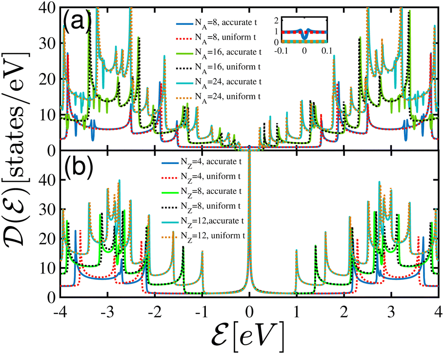


 for different scattering channel lengths. These results are in good agreement with ref. 55. Furthermore, from panel (b) we can see an increase in the conductance of 4-ZGNR when there is only one super unit cell in the central channel. This could be due to the overlap between electrodes. However, for longer scattering channels, the transmission probability declines around the zero-energy which shows that for narrow 4-ZGNRs, the two valleys in the band structure are not well separated in momentum space and the flat bands have a limited curvature. Thus, if one considers a sufficient wider ribbon, the transmission probability will completely recover at the Fermi level.26
 of GNRs with 2DG hopping parameters.
 of GNRs with 2DG hopping parameters.
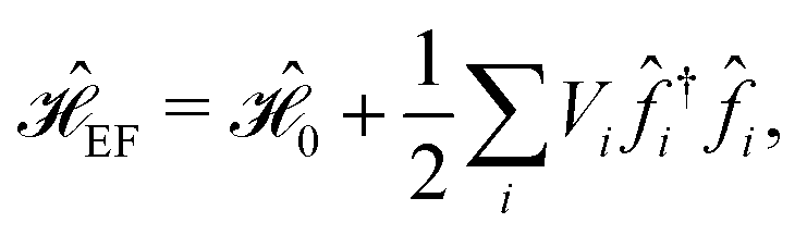
 . Similar to 8-AGNR, an increase in the strength of the applied PEF boosts the zero-transmission region of 4-ZGNR. Electric field-induced 4-ZGNR with an SD hopping parameter shows a strong electron–hole symmetry breaking in the inter-valley scattering of holes and electrons and therefore the transport properties. Interestingly, we found that electric field-induced 4-ZGNR with SD hopping parameters suffers from a metal-to-n-doped semiconductor phase transition because of the electron–hole asymmetry in this material. Thus, it is expected that if one changes the sign of the applied PEF, i.e. through application of a negative bias voltage, a metal-to-p-doped semiconductor phase transition will emerge in 4-ZGNR with realistic hopping parameters. To support this statement we have plotted the electronic band structure and DOS of 4-ZGNR with SD hopping parameters under the application of (a) Vb = +2.5 eV and (b) Vb = −2.5 eV shown in Fig. 13. As illustrated in the figure, the application of PEF makes a shift in the degeneracy of the flat bands at the Fermi level, and consequently, band gap opening is observed. From panel (a) it is clear that for the case of applying a positive electric field, there is a band gap from 0 to 0.62 eV in the conduction band, while the energy gap appears at −0.62 to 0 eV in the presence of negative PEF [panel (b)].
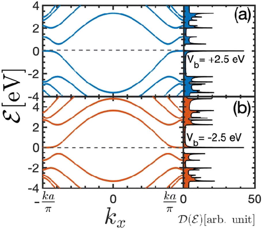
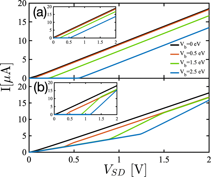
 implies induced momenta by impurities belonging to the FBZ.


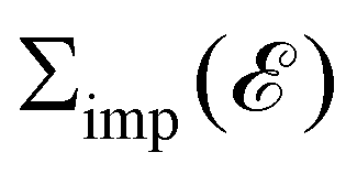 of the disordered system is a state-independent constant for electron-impurity interaction

 of the system in the presence of charged dilute impurity can be computed by substituting the perturbed Green's function in eqn (13) into eqn (6). Eventually, substituting the calculated
  of the perturbed system into the Landauer–Büttiker formula, eqn (7), gives the currents of the impurity-imbrued system as a function of the voltage.
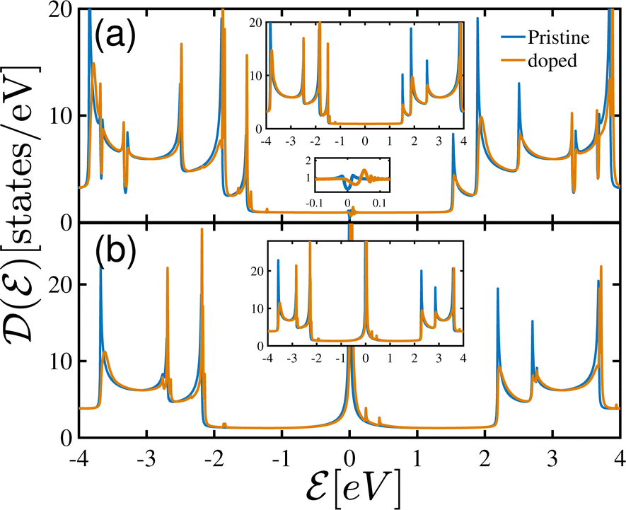
 . Moreover, it is found that no extra zero transmission channels are observed in the transmission spectra of GNRs subjected to dilute charged impurities. Besides, extra dips are found in the zero-bias transmission spectra of 4-ZGNRs around the Fermi level in panel (b) which results from the strong localization of electronic states in these systems. For further study, we carried out the above calculations for the case in which the dilute charged impurity and bias potential are applied to the system simultaneously which are shown in panels (c) and (d). Again, the interaction between impurity atoms and the charge carriers in GNR makes a depopulation of the sub-bands, and consequently
  decreases by increasing the impurity concentration. Moreover, electron–hole symmetry breaking is found in the transmission spectra of all considered systems in the presence of electron-impurity interaction effects which is directly related to the appearance of the electron–hole asymmetry in their band structure. As demonstrated in the lower panels (c) and (d), the application of PEF enhances the electron–hole asymmetry of impurity-induced GNRs, thus more extra dips are observed. Our findings are in good agreement with ref. 65 in which such decrements in transmission coefficient of impurity-doped GNRs with zig–zag edges have been observed.
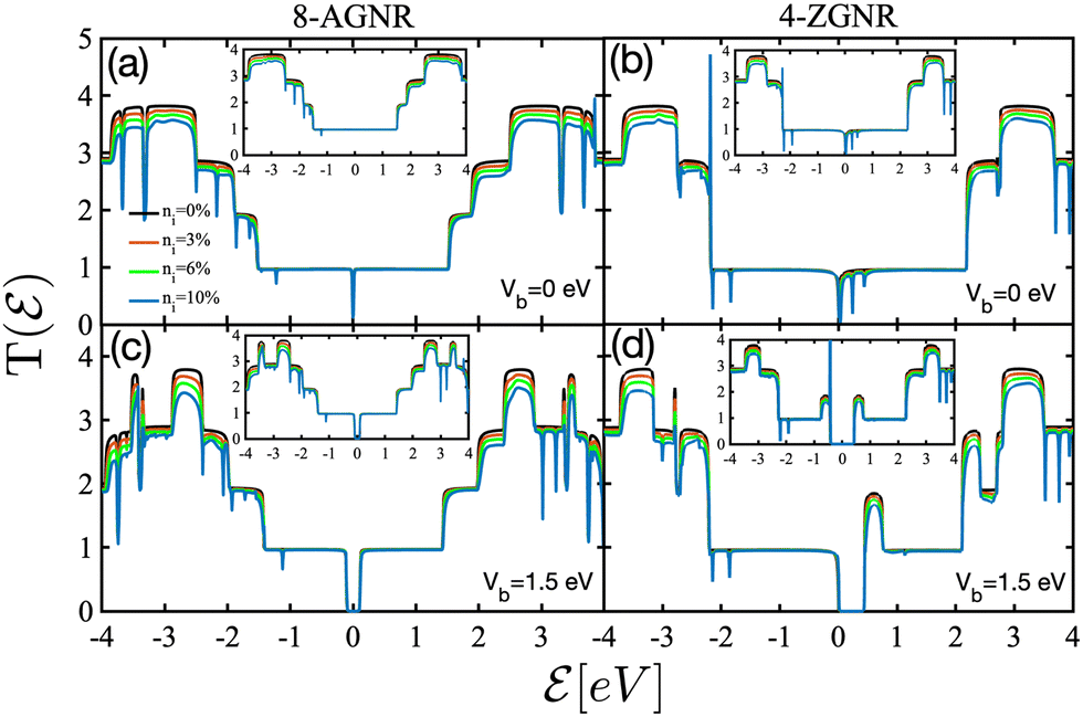

 disappears especially at energy levels far from
  for stronger scattering potentials. A comparison between Fig. 16 and 18 reveals that the strength of scattering potential plays a more effective role than the impurity concentration in controlling the transport properties of GNRs.