
 Open Access Article
 This Open Access Article is licensed under a
 Creative Commons Attribution 3.0 Unported Licence
Enabling cryogenic gravitational wave detectors: growth of sapphire crystals with record low absorption in the near infrared
T.
Aventin
a,
A.
Nehari
a,
D.
Forest
b,
J.
Degallaix
b,
C.
Dujardin
 a,
G.
Cagnoli
a and
K.
Lebbou
a
a,
G.
Cagnoli
a and
K.
Lebbou
a
aInstitut Lumière Matière (ILM), UMR 5306 Université Lyon1-CNRS, Université de Lyon, Lyon 69622, Villeurbanne Cedex, France. E-mail: kheirreddine.lebbou@univ-lyon1.fr
bLMA – CNRS/IN2P3 Laboratoire des Matériaux Avancés, 69100 Villeurbanne, France
First published on 2nd August 2024
Abstract
15 ultra-pure sapphire single crystals of 32 mm diameter and 100 mm long were grown under a stationary stable regime using the Czochralski (Cz) technique. Despite varying several growth parameters, the obtained crystals were transparent without visible macroscopic defects such as cracks, inclusions and grain boundaries. The optical absorption coefficients (α) at the 1064 nm wavelength of the grown sapphire crystals were mapped by Photothermal Deflection Spectroscopy (PDS). The crystals grown along c-axis using low pulling rates lower than 1.5 mm h−1, at 1064 nm present an very low optical absorption coefficients (α = 11 ppm cm−1). At such low levels, the origin of the optical absorption has never been explained. However, in this paper we point toward the role of Fe2+–Fe3+ and Ti3+–Ti3+ pairs. These results open the route to upscaling the growth process to achieve ultra-large sapphire crystals with outstanding optical performances, which are a key for the next generation of gravitational wave detectors.
1. Introduction
With the first direct gravitational wave (GW) detection in 2015,1 the universe has started to be explored by a completely new messenger. After exploiting all bands of the electromagnetic spectrum, GW detection opened a new window on the universe, enabling the regular study of extragalactic objects.Space–time deformations produced by the gravitational waves are measured by monitoring the position of mirrors suspended in a Michelson interferometer configuration, whose sensitivity to mirror displacements is enhanced by the use of km long Fabry–Perot cavities in each arm.2 All the signals detected so far came from the merger of compact objects such as black holes (BHs) or neutron stars (NSs). Signals from supernovae (SN), pulsars and more exotic phenomena such as the cosmic string or the cosmic microwave background3 have yet to be detected. Such phenomena need a controlled technology and high quality materials.
Among those materials, sapphire is a unique material combining excellent mechanical properties with exceptional optical performance.4–6 It is the second hardest material after diamond and it has a very wide optical transmission band ranging from UV (λ ≈ 200 nm) to midinfrared (λ ≈ 5 μm).7–9 It also has excellent thermal properties with a very high congruent melting point of 2050 °C and a very high thermal conductivity.10,11 It is therefore naturally used in a wide range of cutting-edge applications ranging from military applications to extreme physics experiments such as gravitational wave detection.12–14
Reaching the true cosmological distances of future cryogenic GW detectors is only possible if a crystalline material with sufficiently low absorption is available in large dimensions. For cryogenic operation, the material must be monocrystalline, as all amorphous materials, such as fused silica used in all room-temperature detectors, have far too high thermal noise levels.15 There are two promising crystalline materials. Silicon, which can be produced by directional solidification in large dimensions required by the GW detector (50 cm diameter),16 has an absorption of several hundred ppm cm−1. Sapphire, currently used for the Japanese gravitational wave detector KAGRA 22 cm diameter mirrors, has an average absorption of 50 ppm cm−1.17 Neither of these materials is compatible with the European Einstein Telescope (ET) requirements.
While promising on paper, some problems with the use of sapphire substrates have been highlighted, most notably its optical absorption at 1064 nm. A higher optical absorption means reducing the laser power to avoid introducing excess heat than can't be extracted from the mirrors while maintaining the mirror nominal temperature. In addition, a lower laser power increases the quantum noise, leading to an overall reduction in the detector sensitivity. Unexpected birefringence despite using c-axis sapphires has also been measured.
Low absorption sapphire removes the main obstacle for any GW cryogenic detector. For the ET, it means being able to have 5 times more laser power and, consequently,  times less quantum noise at 30 Hz. Birefringence effects degrade the sensitivity of gravitational wave detectors, not only because they introduce optical losses, but also because spatial fluctuations create extra phase noise in the arm cavity reflected beam.18 As sapphire is a birefringent material with its optical axis along the c-axis, substrates for the GW detector mirrors must be aligned along the c-axis.
In this work, we report the Czochralski growth of 3.5 cm-diameter sapphire single crystals that exhibit a record absorption of 10 ppm cm−1 in a controlled and repeated manner to investigate the origin of this absorption.
2. Experimental section
2.1 Crystal growth
Under a stationary stable growth regime, 15 sapphire bulk single crystals were grown by the Czochralski technique, using the same oven in an argon atmosphere.19–21 To ensure that the melting temperature crystal growth is maintained, the control program freely controls the generator heating power output. Two oriented seeds were used for pulling crystals from the melt, one for the c-axis and another one for the a-axis.The raw materials used were high purity sapphire crackles grown by RSA Le Rubis Company22 using the Verneuil growth method. Glow discharge mass spectroscopy (GDMS) analysis of the feed material used in the experiments is shown in Table 1. It can be seen that most elements are close to their detection limit for the analysis, confirming the high purity of the used starting raw material.
| Fe | Cr | Ti | Co | Ni | Mn | V | Ir | Na | Si | P | Cl | K | Ga |
|---|---|---|---|---|---|---|---|---|---|---|---|---|---|
| 1.7 | 0.28 | 0.75 | 0.08 | <0.05 | <0.05 | <0.05 | <0.1 | 12.5 | 2.4 | 1.2 | 1.5 | 2.3 | 2.7 |
2.2 Optical absorption measurement
The 1064 nm absorption coefficient mappings of the sapphire samples were measured using the Photothermal Deflection Spectroscopy (PDS) technique23 (Fig. 1a). This method uses the mirage effect to obtain a precise measurement of the absorption coefficient α inside the volume of a transparent material. A high power laser at 1064 nm is focused inside the substrate, where a very small amount of light is absorbed (Fig. 1b). The absorbed light is converted to heat creating a gradient of temperature inside the sample. A second laser at a different wavelength is deflected by this gradient. The absorption coefficient is directly proportional to the deflection of this probe laser recorded using a quadrant detector. | ||
| Fig. 1 Picture of the PDS bench (a) and schematic diagram of a collinear 1064 nm PDS bench (b). | ||
Since the tested samples are mounted on transverse displacement stages, it is possible to do a 2D mapping of the absorption. For this paper, a mapping on a diameter of 30 mm on each sample was performed with a lateral step size of 2 mm. To study the absorption along the crystal growth direction, each crystal was cut in 3 or 4 pieces along the growth axis. As can be seen in Fig. 1b, the signal detected by the quadrant detector is then read using a lock-in amplifier. This is because the pointing instability of the probe beam (or beam jitter) is a major noise source of this technique at low frequency. In order to mitigate the impact of this noise, the pump beam intensity is modulated at a high frequency. The lock-in amplifier then extracts the signal from the quadrant detector at the given modulation frequency.
3. Results and discussion
3.1 Czochralski sapphire crystals grown from the melt
The cylindrical shaped crystals were grown with a total length of 100 mm and a diameter of 35 mm. The experimental apparatus allowed for a control of the different growth parameters, and in particular the pulling and rotation rates, the rod rotation speed (the speed at which the rod that holds the crystal turns) and the crucible counter rotation speed (the speed at which the whole structure turns, in the opposite direction to the seed).The rotation speed is an important parameter for two reasons. The first one is that it allows obtaining the desired circular cross section. Without any rotation, the crystal will grow faster along a specific direction corresponding to minimum heat transport from the melt to the crystal. If the machine does not have perfect thermal symmetry along the vertical axis coincident with the growth directions, the crystal would wander off the pulling axis producing an object with a spiral shape and without any symmetry and strong variations in diameter (Fig. 2). The second one concerns the distribution of the unwanted impurities coming from the initial raw materials. Without any rotation, the impurities in the melt would be subjected to the effect of the natural convective flow in the melt. This flow is driven principally by the buoyancy created by the temperature field. Finally, the crucible rotation also affects the geometry of the crystal–melt interface, an important factor in controlling crystal perfection.
 | ||
| Fig. 2 Sapphire ingot grown without an automatic program showing diameter instability. | ||
All the crystals grown were then cut into 15 mm thick cylinders (30 mm in diameter) and polished on both sides to obtain a transparent sample. Photos of the as-grown sapphire crystals, as well as the samples cut and polished from the crystals, are presented in Fig. 3. The grown crystals present a high macroscopic surface quality and controlled shape. They are free of macroscopic defects. The crystals grown along the a-axis presented two facets and along the c-axis, they present a hexagonal shape with six facets. The most observed defects in the Czochralski crystal growth technology are gaseous and solid inclusions and grain boundaries.24 The reason for such a defect origin is crystal super-cooling and hence the loss of the crystallization stability front. In order to overcome these problems and to control the growth conditions at the crystallization interface and prevent the formation of related defects, an automatic control system using a crystal weight sensor was applied to the process. The growth parameters used for each crystal are summarized in Table 2 and the average absorption (discussed later) has been added. We did GDMS analysis on three samples (Table 3). When looking at the first seven elements, we can see that the concentrations for cobalt, nickel, manganese and vanadium are very low, below 0.1 ppm for these 4 elements (with the exception of nickel in sample 193). There is however between a few and a few tenths of ppm of iron, chromium and titanium in all three of these samples. The phosphorus concentration goes from 3.6 ppm in 191 to less than 0.005 ppm in 196 or chlorine with 191 displaying 16 ppm and 193 and 196 having 0.52 and 0.07 ppm, respectively.
 | ||
| Fig. 3 Top: Picture of the sapphire crystals grown under a stationary stable regime. Bottom: Different samples of 15 mm thick cylinder prepared from sapphire ingot. | ||
| Crystal reference | Crystal orientation | Pulling rate (mm h−1) | Rod rotation speed (rpm) | Crucible rotation speed (rpm) | Mean α at 1064 nm (ppm cm−1) |
|---|---|---|---|---|---|
| 191 | A | 2 | 4 | 0 | 56 |
| 192 | C | 2 | 4 | 0 | 44 |
| 193 | C | 2 | 8 | 0 | 38 |
| 194 | C | 2 | 16 | 0 | 33 |
| 196 | C | 1.5 | 4 | 0 | 17 |
| 197 | C | 2 | 4 | 1 | 18 |
| 198 | C | 2 | 12 | 1 | 24 |
| 199 | C | 2 | 12 | 0 | 22 |
| 204 | A | 2 | 8 | 0 | 44 |
| 205 | C | 2 | 4 | 0 | 15 |
| 206 | C | 1.5 | 12 | 0 | 11 |
| 207 | C | 1 | 4 | 0 | 11 |
| 212 | C | 1 | 6 | 0 | 10 |
| 213 | C | 1 | 4 | 1 | 20 |
| 214 | A | 1 | 4 | 1 | 44 |
| Chemical elements | 191 (ppm) | 193 (ppm) | 196 (ppm) |
|---|---|---|---|
| Fe | 2.8 | 3.7 | 1.5 |
| Cr | 0.37 | 1.3 | 0.42 |
| Ti | 0.85 | 0.66 | 0.91 |
| Co | 0.07 | <0.05 | <0.05 |
| Ni | <0.05 | 0.26 | 0.06 |
| Mn | <0.05 | 0.08 | <0.05 |
| V | <0.05 | <0.05 | <0.05 |
| Ir | <0.1 | <0.1 | 5.2 |
| Na | 15 | 6.9 | 11 |
| Si | 5.8 | 1.3 | 2.3 |
| P | 3.6 | 0.26 | <0.005 |
| Cl | 16 | 0.52 | 0.07 |
| K | <0.5 | 5.3 | 0.07 |
| Ga | 3.6 | 0.35 | 3.2 |
3.2 Mean absorption
Table 2 presents the growth parameters and the crystal mean absorption coefficients of 15 samples cut from the sapphire crystal samples. The numbers attributed to each crystal are related to the order in which they were produced, 191 being the first and 214 being the last. The mean absorption coefficients of the crystals were calculated by averaging the mean absorption coefficient (α) of each sample from the same crystal.We obtain very low absorption coefficients for all our crystals, ranging from 56 ppm cm−1 (191) for the highest to 10 ppm cm−1 for the lowest (212). Although these results are achieved on much smaller crystals than the ones used as test masses in KAGRA (220 mm in diameter and 150 mm thick), this is to our knowledge the first time that reproducible absorption coefficients of less than 50 ppm cm−1 have been obtained in a repeated manner.
Growth along the c axis tends to demonstrate a lower absorption coefficient than growth along the a-axis. For example, when comparing crystals 191 and 192 in particular, we can see that the average absorption coefficient goes from 56 ppm cm−1 to 44 ppm cm−1 when changing the crystalline direction from the a-axis to the c-axis, while keeping the other growth parameters identical. The growth along the c-axis leading to lower 1064 nm absorption levels is very beneficial to cryogenic GW detectors, as in any case the c-axis is necessary to limit detrimental birefringence effects.18
It can also be noticed that the first series of the four crystals pulled shows a much higher α coefficient than the other ones (the 204 and 214 a-axis crystals), ranging from 56 to 33 ppm cm−1 with the absorption coefficient being lower after each crystal growth. From this first series, it seems like the higher the rotation speed, the lower the absorption coefficient. It can also be noted that in this first series of crystals, the absorption lowered after each growth.
In order to correlate the growth parameters to the absorption coefficients, Fig. 4 presents the absorption coefficients α as a function of the rod rotation rate for samples 196 to 199 and 205 to 213. These samples were chosen as they were all grown along the c-axis. When we compare the samples grown with the same rod rotation speed, whatever the pulling rate and the rotation rate we can see that the sample grown with the counter rotation (crucible rotation) have a higher α absorption coefficient than the ones grown without crucible rotation.
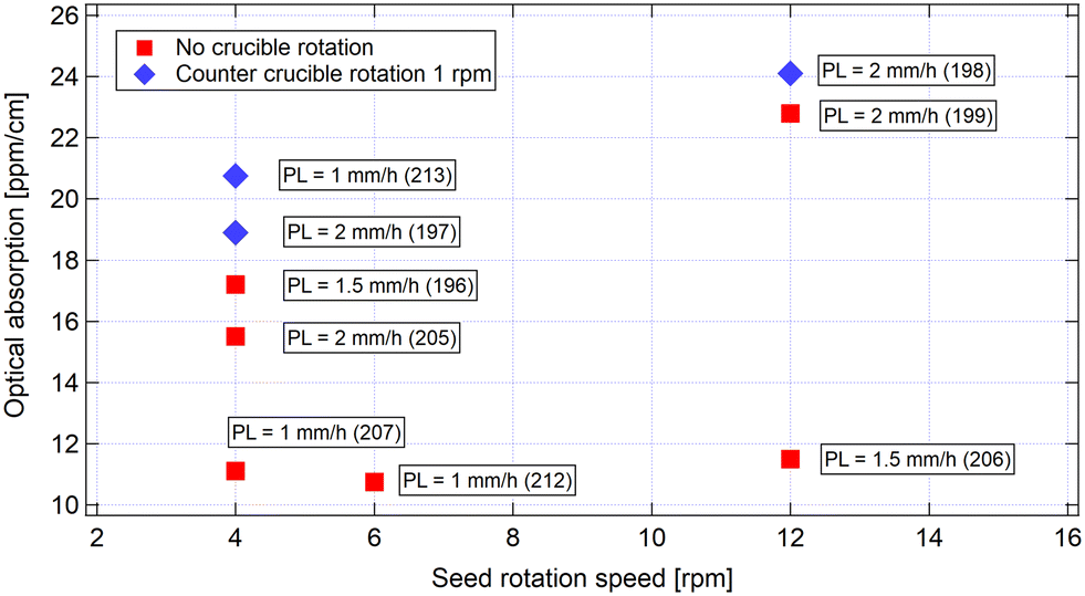 | ||
| Fig. 4 Evolution of the optical absorption coefficient (α) as a function of rotation rate (rpm) and pulling rate (mm per hour). | ||
When looking at the pulling rate variations, there does seem to be a reduction of the absorption coefficient with the lowering of the pulling rate, independent of the lowering of the absorption over time in our experiment. In particular, the latest crystals 206, 207 and 212 showed average absorption coefficients of 11 ppm cm−1, 11 ppm cm−1 and 10 ppm cm−1 respectively. Pulling the crystal at a low pulling rate (1 mm per hour) does seem to help the obtainment of high quality crystal in regard to the 1064 nm absorption.
This result was expected as lowering the pulling rate gives more time for the crystallization kinetics and limits stress propagation and dislocation density25 and allows for a better structure regarding lattice relaxation, which could be beneficial to obtain the lowest absorption.
Finally, the three samples (197, 198 and 213) grown with the crucible counter rotation turned on (crucible rotation) show moderately higher optical absorption values (18 ppm cm−1, 24 ppm cm−1 and 20 ppm cm−1) compared to similar samples without counter rotation. This indicates that the counter rotation has no beneficial effect regarding the optical absorption. Increasing the pulling rate to 2 mm per hour and rotation rate >4 rpm degrades the absorption coefficient (α > 20 ppm cm−1). In Fig. 5, the pulling rate and seed rotation rate affect the absorption coefficient. There is a critical balance between these two parameters and they can compensate each other.
 | ||
| Fig. 5 2D optical absorption maps of the sapphire crystals as a function of position and growth parameters. | ||
3.3 Optical absorption uniformity
The absorption mappings of each individual sample give information about the spatial distribution of the optical absorption. Fig. 5 shows the absorption maps of the sapphire single crystals grown under a stationary stable regime using the Czochralski process with the horizontal and vertical axes representing the position in mm and the α absorption coefficient in ppm cm−1 being displayed by the colour scale. On nearly all the samples, the closer you are to the edge, the higher the absorption coefficient, with its value doubling between the centre and the edge. This effect is clearly visible in most of the maps in Fig. 5.As each crystal was cut in 3 or 4 samples along the growth axis (Fig. 6), it is also possible to study the evolution of the absorption from head to tail, as presented in Fig. 7. On the majority of crystals, we found that the overall trend is an increase of the absorption as we get closer to the tail. We suppose that this is caused by the lowering of the melt level inside the crucible during growth. This changes the thermal gradients of the melt, leading to higher defects and therefore higher absorptions. The most homogenous samples regarding the absorption are the ones with the lowest pulling rate.
 | ||
| Fig. 6 Example of the two different cuts done on our crystals. The top shows how the first eight crystals were cut, with 5 samples cut and polished but only the three in the middle being exploitable. H and T stand for head and tail, respectively. On the bottom, the second cut yielded 4 usable samples. | ||
 | ||
| Fig. 7 Evolution of the absorption maps along the thickness for two different representative crystals. The colour scale is identical for all samples from the same crystal. From left to right, samples from the head to the tail. | ||
On some samples, a high local absorption point was measured, as we can see in the maps of samples 204-3 and 205-2 in Fig. 8. These absorbing points can vary greatly in intensity as we can see that on sample 204-3 we have an absorption of 400 ppm cm−1 when the rest of the sample shows values for α under 50 ppm cm−1 where on sample 205-2 there is a local increase of about 60 ppm cm−1, going from 20 ppm cm−1 in the surrounding points to 80 ppm cm−1 on the absorption point. The increase is lower on sample 193-4 (close to the tail), going from around 30 ppm cm−1 to 42 ppm cm−1 on the “absorption point”. The cause of these local high absorption defects is not yet understood and their interpretation has to be done carefully.
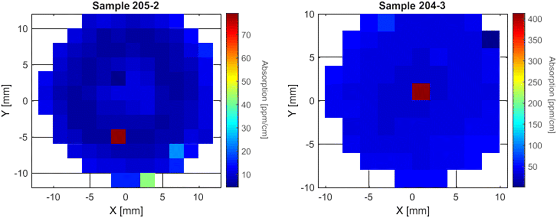 | ||
| Fig. 8 Example of two crystal samples with well-localised points with much higher absorption than the surroundings. | ||
These local absorption points can also be caused by local closest neighbour defect clusters composed of iron or titanium ions in aluminum sites.26
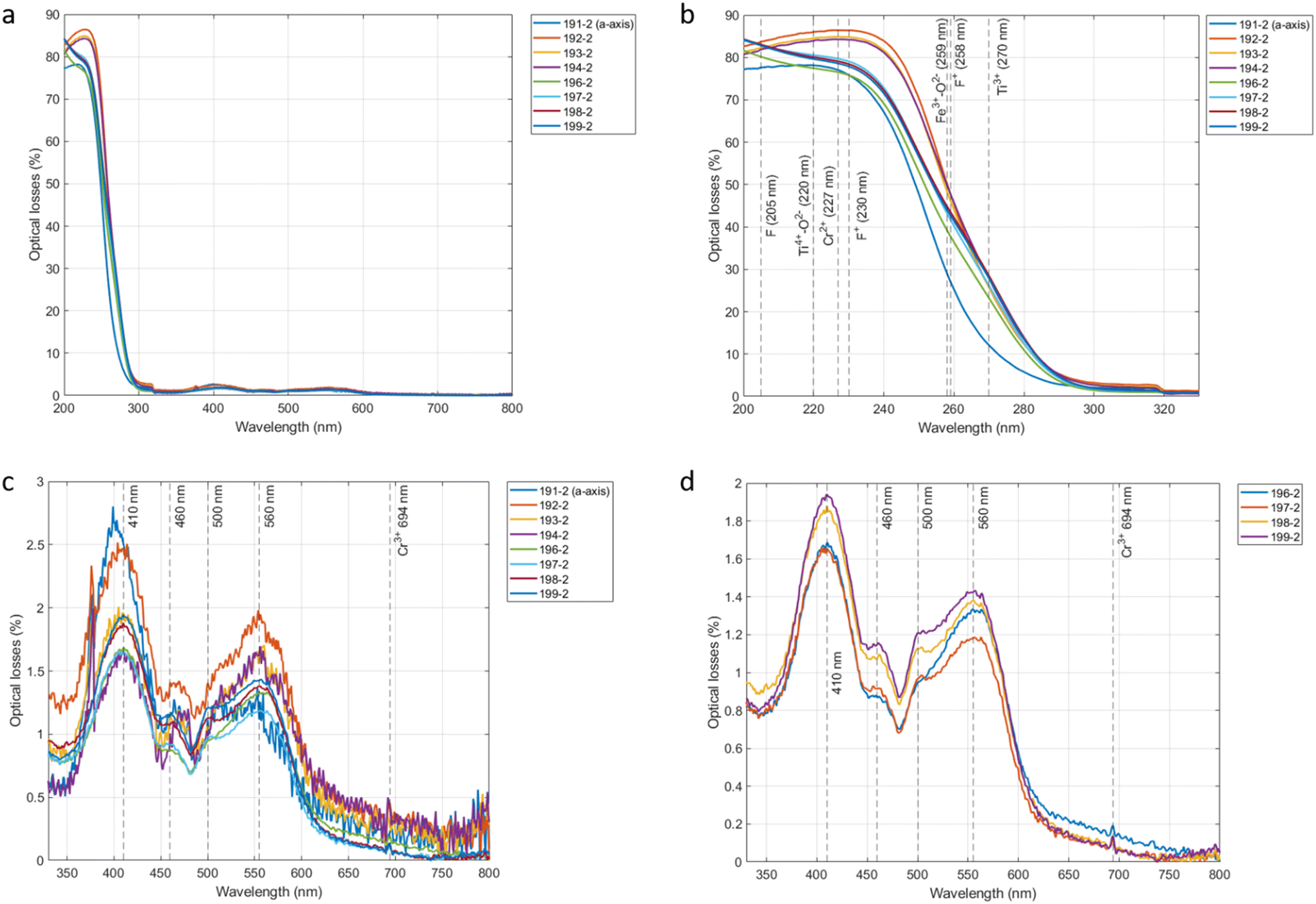
The optical losses of eight different crystals from 200 to 800 nm are plotted in Fig. 9a. We are not aware of any direct correlation in the absorption between the visible and the near-infrared (1064 nm) spectra. However, the absorption bands in the visible wavelength give information about the presence of optically active elements and could hint at the culprits behind the 1064 nm absorption. The baseline of the losses was offset, as it is not dependent on the samples themselves but rather on several external factors, including the temperature, humidity level, as well as on the polishing and calibration of our apparatus. All our crystals display very similar loss spectra.
 | ||
| Fig. 9 (a) Optical losses of 8 samples taken from the middle of 8 different crystals measured from 200 to 800 nm. (b) Optical losses of the 8 samples measured from 200 to 330 nm. (c) Optical losses of the 8 samples measured from 330 to 800 nm. (d) Optical losses of 4 samples measured from 330 to 800 nm. | ||
In Fig. 9, two different sharp regions can be seen: the first between 200 and 330 nm where we measure a very fast increase in the optical losses from the base level of 5 to 10% at 300 nm to over 80% at 200 nm. The second region, from 330 to 800 nm, shows much lower variations that are difficult to see as the spectra are dominated by the first region. For this reason, the spectra were plotted between 200 and 330 nm in Fig. 9b and between 330 and 800 nm in Fig. 9c.
In the 330 to 800 nm range, the spectra of samples 191-2 to 194-3 have a much lower signal to noise ratio. To allow for an easier identification of the peaks, we have also plotted the spectra of only the samples from crystals 4 to 8 in Fig. 9d. At these wavelengths, the majority of absorbing defects are caused by the presence of isovalent (Cr3+, Ti3+, Co3+, Ni3+, Fe3+, Mn3+, V3+) transition metal impurities in aluminium lattice sites.27,28 In other words, optical absorption in the visible wavelengths is mostly caused by the substitution of an Al3+ ion by another 3+ ion. Transition metals in a 3+ ionic state lose their 4s electrons and have incomplete 3d shells. These electrons interact with the surrounding crystal field which results in them having several low energy levels in which optical transitions can occur. These optical transitions lead to absorptions in the visible wavelength and give colour to the crystal.
This is seen in natural sapphires, where the natural blue colour of sapphires is caused by Fe3+ and Ti3+ ions and the red colour of ruby by Cr3+.29–34 When aluminium sites are occupied by divalent ions such as Mg2+ or Be2+, their charge is compensated by O1− ions instead of the normal O2− valence state. These O1− ions are called trap holes and these holes then pair with Cr3+ or Fe3+ producing a strongly absorbing colour centre giving sapphires a characteristic orange (called padparadscha) and yellow colour, respectively.33,34 These colour centres only appear in sapphires grown or heat-treated in an oxidising environment and are therefore not expected on our sapphires grown in an argon gas atmosphere.
In our undoped sapphires, there is no dominant effect of a particular dopant over all other impurities. This leads to a fit of the absorption spectra containing many Gaussian contributions which will mathematically always produce a satisfying fit regardless if it has physical meaning or not. It becomes impossible to give any physical sense to the choice of a particular Gaussian fit over another. Instead, we have identified 5 bands in particular on our spectra and will try to present the possible multiple contributions of these bands: two large bands centred at 410 and 560 nm, two smaller shoulders at 460 and 500 nm and 530 nm and one thin peak at 694 nm.
The first broad band from 380 to 450 nm and centred at 410 nm seems to correspond to the “residual absorption” peak found in Ti-doped sapphires and is attributed to Ti3+ by Moulton et al.35 The exact process that creates this absorption is not known but the intensity of this peak is dependent on the square of the Ti3+ concentration in Ti-doped sapphires, indicating the role of Ti3+ pairs. Another likely contribution is the transition of a Cr3+ 3d electron from 4A2 to 4T1 absorbed at 409 nm.28,33,36,37 Other contributions could come from the second excitation of a 3d electron of V3+ absorbed at 401 nm (ref. 28 and 33) or an aluminium vacancy closest neighbour with an OH− defect absorbed at 413 nm.38,39
As the first band decreases, a small shoulder around 460 nm is visible before a sharp decrease at 480 nm. This peak could be caused by two main contributions: the 450 nm absorption peak of Fe3+–Fe3+ pairs caused by the excitation of one 3d electron from the ground state to the 4A1 energy level,29,33,40–42 and the absorption caused by an F2+2 centre (two F+ centre closest neighbours) at 455 nm.43–45
The third band is similar to the previous one in the sense that it appears as a small shoulder on top of a larger Gaussian peak and is centred around 500 nm. This could correspond to the main absorption of Ti3+ doped sapphires used in lasers called the pump band which is a broad absorption peak from 400 to 700 nm composed of a high band centred at 490 nm and a second low band around 560 nm.28,35,46 This two-peaked absorption corresponds to the excitation of a 3d electron of Ti3+ from its ground level 2T2 to its first excited state 2E which is split in two by the Jahn–Teller effect.
It should be noted that in Ti doped sapphire, the first 490 nm peak has a higher intensity than the second 560 nm peak while we observe the opposite on our samples. This supports our hypothesis that in our undoped sapphire, this peak has multiple sources. Such sources can be the 558 nm 4A2 to 4T1 transition of Cr3+,28,37,47 the first excitation of a 3d electron of V3+ at 570 nm (ref. 28, 47 and 48) and the Fe2+–Ti4+ closest neighbour pair inter-valence charge transfer at 570 nm.27,31,40,47 While this pair has been attributed to the characteristic blue colour of natural sapphire, recent work with X-ray absorption near-edge spectroscopy (XANES) has suggested that this absorption peak is due to an Fe3+–Ti4+ mixed acceptor state with two energy levels above the valence band of sapphire.49 Lastly, the thin band at 694 nm is the Raman activated R1 and R2 peak of Cr3+ that was previously measured.28,37,48
Despite having two possible vanadium peaks in our analysis, the very low concentrations of vanadium found through GDMS reduce the likeliness of these optical centres having a visible contribution to our spectra. As no other coloured centre with an OH− defect was found in the spectra, we have also ruled out the aluminium vacancy closest neighbour with an OH− defect absorbed at 413 nm from our possible explanations. The 455 nm peak of the F2+2 centre is usually associated with the presence of the 357 nm peak of the F+2 centre (one F+ and one F centre closest neighbours) which is not measured in our spectra, reducing the plausibility of this peak.
This leaves only peaks attributed to chromium, titanium and iron, which are also correlated to the stronger measured presence of these three elements when compared to other 3+ transition metals. As mentioned earlier, the measured spectra on our sapphires do not show clear single Gaussian peaks, but instead complex absorption bands. These bands are created by the interaction of multiple absorption sources of varying intensities all contributing to the larger overall band. Taking this into consideration, we attribute the first 410 nm peak to a combination of the 409 nm Cr3+ absorption and the 410 nm Ti3+ pair absorption. The small shoulder around 460 nm is attributed to the 450 nm Fe3+ absorption peak, and the 10 nm wavelength difference is likely due to the difficulty in identifying the peak centre due to the much more intense 410 nm peak. The wavelengths of these peaks can also change by up to 10 nm depending on the authors, further confirming the choice of attributing Fe3+ to this peak. For the same reasons, we attribute the 500 nm peak to the first Ti3+ split 3d electron transition that produces a broad peak centred at 490 nm. The large peak around 560 nm is attributed to both the second Ti3+ split 3d electron transition and Cr3+ at 560 and 566 nm, respectively. Lastly, the small peak at 694 nm is easily attributed to Cr3+.
All the absorption peaks of both Cr3+ and Ti3+ ions have been attributed to absorption features in our measured spectra,34,35 further corroborating the peak assignments. The Fe3+ peak attribution is less clear, while the 450 nm absorption of Fe3+–Fe3+ pairs does seem to be present; the presence of the two other major Fe3+ peaks is less evident. This is the 3d electron excitation of one of the two Fe3+ ions in a Fe3+–Fe3+ pair from the ground 6A1 state to 4E absorbed around 377 nm and the excitation of a single Fe3+ 3d electron from 6A1 to 4T2 at 388 nm.28,29,33,40–42 Fe3+ ions have an absorption cross section in the 400 to 700 nm range, one order of magnitude lower than that of Cr3+ or V3+.33,34 This means that at the same concentration, the absorption intensity of Fe3+ is much lower than that of Cr3+. The concentrations of these elements in our samples were shown to be between tenths to a couple of ppm by the GDMS analysis (see Table 3). It is therefore expected that the absorption peaks caused by Fe3+ have a lower intensity than the ones caused by Cr3+. This means that the two 377 and 388 nm peaks are likely present in our spectra but are hidden by the much more intense combined absorptions of Cr3+ and Ti3+ pairs at 409 nm and 410 nm respectively.
The last absorbing defect that could be present in our samples is the Fe2+–Ti4+ intervalence charge transfer (or the Fe3+–Ti4+ mixed acceptor state) which displays two absorption peaks at 580 and 700 nm. While the first peak could be present but hidden in the much more intense peaks of Ti3+ and Cr3+ around 560 nm, the second peak at 700 nm was not detected on our samples, meaning that this absorbing defect is not present in quantities that would create detectable absorptions using our spectrometer. Although this pair has a very high absorption cross section in the 400 to 700 nm range one order of magnitude greater than Cr3+, in the Czochralski grown sapphires, the Fe2+–Ti4+ pairs are largely dissociated due the high growth temperature (2050 °C) and very few pairs exist33 and thus don't contribute visibly to the absorption of our samples.
The identified colour centres behind each of the peaks of our measured optical loss spectra between 330 and 800 nm are summarised and presented in Table 4.
| Absorption peak | Defects | Comment |
|---|---|---|
| 410 nm | Fe3+–Fe3+6:A1 → 4E (377 nm) | Likely hidden by more intense peaks |
| Fe3+6:A1 → 4T2 (388 nm) | ||
| Cr3+4:A2 → 4T1 (409 nm) | Likely hidden by more intense peaks | |
| Ti3+–Ti3+ (410 nm) | ||
| 460 nm | Fe3+–Fe3+6:A1 → 4A1 (450 nm) | 10 nm offset |
| 500 nm | Ti3+:2T2 → 2Ea (490 nm) | 10 nm offset |
| 560 nm | Cr3+4:A2 → 4T2 (558 nm) | |
| Ti3+:2T2 → 2Eb (560 nm) | ||
| 694 nm | Cr3+4:A2 → 2E (694 nm) | Two peaks at 693 and 694.4 nm |
Fig. 9b presents the optical loss spectra between 200 and 330 nm. As mentioned earlier, the spectra present a very steep increase in optical losses from 5 to 10% at 300 nm to over 80% at 220 nm in a linear-like fashion, making peak identification complicated.
The sudden decrease in optical losses at 320 nm is a measurement artefact due to the change in the lamp used with the spectrometer. In the 200 to 330 nm wavelengths, several types of defects can be responsible for optical absorption in sapphires. In particular, F centre type defects, which are one or two electrons trapped in an oxygen vacancy, have several absorption peaks. F+ centres (one electron trapped in an oxygen vacancy) have three transitions from its base energy level which absorb at 197, 230 and 258 nm.
F centres (two electrons trapped in an oxygen vacancy) have an intense absorption at 205 nm.27,37,38,43,50
Impurity type defects also have electron transition levels or charge-transfers that cause absorption in this range. As it is difficult to extract specific peaks from the spectra, only the ones caused by our known optically active elements will be presented: titanium, chromium and iron. Studies on titanium-doped sapphires have shown that a charge-transfer process where O2− exchanges an electron to a Ti4+ ion absorbs strongly at 220 nm.35,51,52 The charge transfer between O2− and Ti3+ is located at 180 nm (ref. 51) and Ti3+ ions also have an absorption at 270 nm but the exact origin of this absorption does not make a consensus.35 The two chromium peaks can affect the absorption in this region: Cr2+ absorbed at 227 nm and the inter-valence charge transfer of Cr3+–O2− absorbed at 180 nm.39,51 In the case of Fe3+, no 3d transition was observed in this wavelength range, but three different Fe4+–O2− charge transfers have been measured at 172, 194 and 259, respectively.33,51
These identified possible absorption peaks are added in Fig. 9b and are referenced in Table 5. A few peaks below our detection limit of 200 nm have also been included as the higher wavelength end of their peak could play a role.
| Wavelength (nm) | 180 | 180 | 194 | 197 | 205 | 220 | 227 | 230 | 258 | 259 | 270 |
|---|---|---|---|---|---|---|---|---|---|---|---|
| Defects | Cr3+–O2− | Ti3+–O2− | Fe3+–O2− | F+ | F | Ti4+–O2− | Cr2+ | F+ | F+ | Fe3+–O2− | Ti3+ pairs |
The samples can be separated into three groups when looking at their optical loss spectra in Fig. 9b: group 1 with 191-3 (which is also the only a-axis sample in this group), then group 2 composed of samples 192-3, 193-3 and 194-4 and finally group 3 with samples 196-2, 197-2, 198-2 and 199-2. In the 260 to 300 nm wavelengths, all the crystals display a very similar increase in optical losses with the exception of 191-3 which shows a slower increase than the other crystals. The sharp optical losses increase with smaller wavelengths in this sample which are also seem to be different to the other groups.
In particular, in this sample the very high absorption feature in the lower wavelength is centred closer the Ti4+ and Cr2+ absorption at 220 and 227 nm than that around the F+ 230 nm absorption. This can also be correlated with a lower overall increase in the optical losses on this sample in the 200 to 230 nm region, which could indicate lower F and F+ concentrations in this sample compared to the others.
While the samples in groups 2 and 3 show a very similar behaviour in the 265 to 330 nm range, the samples in group 3 display a steeper increase in their optical losses. It is not clear whether this steeper increase is a combined effect of the peaks both below (Ti4+, Cr2+, F+) and above (F+) or if there is a contribution by a non-identified absorption feature.
Lastly, unlike the other samples which have a small decrease in the optical losses from 220 to 200 nm, the optical loss of the samples in group 3 continues to increase up to 200 nm. This indicates a stronger influence of absorption features under our detection limit of 200 nm on these samples compared to the others, such as the 197 nm absorption of F+ centres or the 194 nm and 180 nm absorptions of the charge transfers of Fe3+–O2−, Ti3+–O2− and Cr3+–O2−.
Overall, the absorption of our samples in the 200 to 800 nm range is caused by both intrinsic defects, in particular F centres caused by oxygen vacancies, and some impurity species, namely chromium, titanium and iron. It is however difficult to extract quantitative data from these measurements as the intensity of each peak not only depends on the concentration of the impurity elements and their respective absorption cross sections, but also on their valence state and on the proximity of other impurity or vacancy defects that could allow for charge transfers.
Comparing the Cr3+ emissions of our crystals to other sapphires with absorptions in the thousands of ppm cm−1 at 1064 nm has shown that our samples contained much more Cr3+ than the higher absorbing crystals. This work is still in progress and will be published later, but this has led us to eliminate chromium as a potential source of absorption at 1064 nm. We have identified two hypotheses on the origin of the optical absorption in sapphire: first, an intervalence charge transfer in face-sharing Fe2+–Fe3+ defect clusters which are absorbed in the 1000–1111 nm range.29,42,53 The second origin pointed toward to the role of Ti3+–Ti4+ pairs in this absorption;54 however, the more recent work by Moulton et al.35 seems to show that this absorption is caused independently by both Ti3+ pairs and the interaction of Ti4+ ions with their associated Al vacancies in complex defect structures.
According to the GDMS (Glow Discharge Mass Spectrometry) results for the 3 crystals, the concentrations of both of these elements (Ti and Fe) are very low with only a few ppm of the total weight. If these defects were distributed uniformly in the bulk, the probability that 2 titanium or iron atoms forming complex defect clusters would be very low.
4. Conclusions
We have successfully grown different undoped sapphire crystals using different growth parameters. The single crystals were crystallized under a stationary stable regime using the a and c-axis orientations. Whatever the selected growth parameters, the crystals are free of macroscopic defects such as cracks and inclusions. Through photothermal deflection spectroscopy, we have successfully mapped the 1064 nm optical absorption of sapphire crystals. In all samples except one sample, we have obtained sub 50 ppm cm−1 absorption, and even an absorption around 10 ppm has been registered. This is the first time such low absorption has been reported on sapphire in a controlled and repeated manner. The comparison of the growth parameters with the absorption has given insight on the influence of these parameters, and we have shown that the c-axis Czochralski grown sapphires display a lower absorption than the a-axis ones. We have also found that both a low pulling rate and a slow rod rotation speed help reduce the absorption, with the pulling rate being the more important parameter. No beneficial effect of the crucible counter-rotation was found. The optical losses of the sapphire samples from 200 to 800 nm have shown that in particular both Cr3+ and Ti3+ play a major role in the visible absorption of our samples, with Fe3+ being less visible but still present. In the shorter wavelengths, these species, as well as F type centers, play a role in the high absorption of the sapphires, although the steep increase in optical losses made peak identification harder. This gives us a first insight on the possible culprits behind the 1064 nm absorption of sapphire.Data availability
All the data supporting this work have been included within the article and are available on request.Conflicts of interest
There are no conflicts to declare.Acknowledgements
The work was supported by the DOSFAP and SEPO450 Projects “AAP Auvergne Rhone Alpe Region”. In the frame of the SaphirLab joint project (Thanks to Labcom ANR program), we are grateful for the great help of RSA Le Rubis Company. The authors are thankful to Dr O. Benamara for the experimental help.References
- LIGO Scientific Collaboration and Virgo Collaboration, Phys. Rev. Lett., 2016, 116, 061102 CrossRef PubMed.
- P. R. Saulson, Fundamentals of Interferometric Gravitational Wave Detectors, World Scientific Books, 2nd edn, 2017 Search PubMed.
- P. Binetruy, A. Bohe, C. Caprini and J. F. Dufaux, J. Cosmol. Astropart. Phys., 2012, 2012, 027 CrossRef.
- V. N. Kurlov, Sapphire: Properties, Growth, and Applications, Encycl. Mater. Sci. Technol, 2001, p. 8259 Search PubMed.
- V. Pishchik, L. A. Lytvynov and E. R. Dobrovinskaya, Sapphire, Springer US, Boston, MA, 2009 Search PubMed.
- F. A. Ponce and D. P. Bour, Nature, 1997, 386, 351 CrossRef CAS.
- P. F. Moulton, J. Opt. Soc. Am. B, 1986, 3, 125 CrossRef CAS.
- N. V. Belov, Structure of Ionic Crystals and Metatallic Phases [Struktura Ionnykh Kristallov I Metallicheskikh Faz into Russian], Academy of the Sciences of the USSR, Moscow, Russia, 1947 Search PubMed.
- F. Schmid and C. P. Khattak, Proc. SPIE, 1989, 1112, 25 CrossRef CAS.
- C. H. Chen, J. C. Chen, C. W. Lu and C. M. Liu, J. Cryst. Growth, 2011, 318, 162–167 CrossRef CAS.
- G. G. Wang, J. C. Han, H. Y. Zhang, M. F. Zhang, H. B. Zuo, Z. H. Hu and X. D. He, Cryst. Res. Technol., 2009, 44(9), 995–1000 CrossRef CAS.
- V. Chandrasekharan and H. Damany, Birefringence of sapphire, magnesium fluoride, and quartz in the vacuum ultraviolet, and retardation plates, Appl. Opt., 1968, 7(5), 939–941 CrossRef CAS PubMed.
- J. Degallaix, C. Zhao, L. Juf and D. Blair, Superiority of sapphire over silicon test masses regarding thermal noise and thermal lensing for laser interferometers with transmissive optics, J. Phys.: Conf. Ser., 2006, 32, 404–412 CrossRef CAS.
- Q. Wen, W. Xinyu, F. Jiang, X. Lu and X. Xu, Focused ion beam milling of single crystal sapphire with a-, c-, and m-orientations, Materials, 2020, 13, 2871 CrossRef CAS PubMed.
- K. Topp and D. Cahill, Z. Phys. B: Condens. Matter, 1996, 101, 235–245 CrossRef CAS.
- F. M. Kiessling, P. G. Murray, M. Kinley-Hanlon, I. Buchovska, T. K. Ervik, V. Graham, J. Hough, R. Johnston, M. Pietsch and S. Rowan, et al. , Phys. Rev. Res., 2022, 4, 043043 CrossRef CAS.
- E. Hirose, D. Bajuk, G. Billingsley, T. Kajita, B. Kestner, N. Mio, M. Ohashi, B. Reichman, H. Yamamoto and L. Zhang, Phys. Rev. D: Part., Fields, Gravitation, Cosmol., 2014, 89, 062003 CrossRef.
- Y. Michimura, H. Wang, F. Salces-Carcoba, C. Wipf, A. Brooks, K. Arai and R. X. Adhikari, Phys. Rev. D, 2024, 109, 022009 CrossRef CAS.
- H. Li, E. A. Ghezal, A. Nehari, G. Alombert-Goget, A. Brenier and K. Lebbou, Opt. Mater., 2013, 35, 1071–1076 CrossRef CAS.
- H. Li, E. A. Ghezal, G. Alombert-Goget, G. Breton, J. M. Ingargiola, A. Brenier and K. Lebbou, Opt. Mater., 2014, 37, 132–138 CrossRef CAS.
- G. Alombert-Goget, H. Li, J. Faria, S. Labor, D. Guignier and K. Lebbou, Opt. Mater., 2016, 51, 1–4 CrossRef CAS.
- RSA Le Ruby Company, https://alumine-rsa.com/ Search PubMed.
- W. B. Jackson, N. M. Amer, A. C. Boccara and D. Fournier, Appl. Opt., 1981, 20, 1333–1344 CrossRef CAS PubMed.
- T. Duffar, Floating zone; Shaping and crucibles techniques, Crystal growth processes bases on capillarity, Wiley, Czochralski, 2010 Search PubMed.
- I. Lasloudji, F. Mokhtari, A. Nehari, G. Alombert-Goget and K. Lebbou, CrystEngComm, 2018, 20, 1110–1115 RSC.
- A. R. Moon and M. R. Phillips, J. Am. Ceram. Soc., 1994, 77, 356–367 CrossRef CAS.
- V. Pishchik, L. A. Lytvynov and E. R. Dobrovinskaya, Sapphire: Material, Manufacturing, Applications, Springer US, Boston, MA, 2009 Search PubMed.
- D. S. McClure, J. Chem. Phys., 2004, 36, 2757–2779 CrossRef.
- J. Ferguson and P. Fielding, Aust. J. Chem., 1972, 25, 1371–1385 CAS.
- L. V. Nikolskaya, V. M. Terekhova and M. I. Samoilovich, Phys. Chem. Miner., 1978, 3, 213–224 CrossRef CAS.
- E. Fritsch and G. R. Rossman, Gems Gemol., 1988, 24, 3–15 CAS.
- C. W. Stillwell, J. Phys. Chem., 2002, 30, 1441–1466 CrossRef.
- E. V. Dubinsky, J. Stone-Sundberg and J. L. Emmett, Gems Gemol., 2020, 56, 1–27 Search PubMed.
- M. Jeršek, G. Jovanovski, B. Boev and P. Makreski, ChemTexts, 2021, 7, 19 CrossRef.
- P. F. Moulton, J. G. Cederberg, K. T. Stevens, G. Foundos, M. Koselja and J. Preclikova, Opt. Mater. Express, 2019, 9, 2216–2251 CrossRef CAS.
- M. E. Innocenzi, R. T. Swimm, M. Bass, R. H. French, A. B. Villaverde and M. R. Kokta, J. Appl. Phys., 1990, 67, 7543–7546 CrossRef.
- F. Benabid, et al. , J. Phys. D: Appl. Phys., 2000, 33, 589 CrossRef CAS.
- K. H. Lee and J. H. Crawford, Phys. Rev. B: Solid State, 1977, 15, 4065–4070 CrossRef CAS.
- T. J. Turner and J. H. Crawford, Solid State Commun., 1975, 17, 167–169 CrossRef CAS.
- J. J. Krebs and W. G. Maisch, Phys. Rev. B: Solid State, 1971, 4, 757–769 CrossRef.
- K. Eigenmann, K. Kurtz and H. H. Günthard, Chem. Phys. Lett., 1972, 13, 54–57 CrossRef CAS.
- A. R. Moon and M. R. Phillips, J. Am. Ceram. Soc., 1994, 77, 356–367 CrossRef CAS.
- B. D. Evans, J. Nucl. Mater., 1995, 219, 202–223 CrossRef CAS.
- G. J. Pogatshnik, Y. Chen and B. D. Evans, IEEE Trans. Nucl. Sci., 1987, 34, 1709–1712 Search PubMed.
- Y. Chen, M. M. Abraham and D. F. Pedraza, Nucl. Instrum. Methods Phys. Res., Sect. B, 1991, 59–60, 1163–1166 CrossRef.
- P. F. Moulton, J. Opt. Soc. Am. B, 1986, 3, 125–133 CrossRef CAS.
- R. M. Macfarlane, J. Chem. Phys., 2004, 39, 3118–3126 CrossRef.
- H. Wang, X. Y. Yu, F. Liu, M. Alam and G. C. Wu, Crystals, 2022, 12, 4 CAS.
- P. Wongrawang, N. Monarumit, N. Thammajak, P. Wathanakul and W. Wongkokua, Mater. Res. Express, 2016, 3, 026201 CrossRef.
- B. G. Draeger and G. P. Summers, Phys. Rev. B: Condens. Matter Mater. Phys., 1979, 19, 1172–1177 CrossRef CAS.
- H. H. Tippins, Phys. Rev. B: Solid State, 1970, 1, 126–135 CrossRef CAS.
- W. C. Wong, D. S. McClure, S. A. Basun and M. R. Kokta, Phys. Rev. B: Condens. Matter Mater. Phys., 1995, 51, 5682–5692 CrossRef CAS PubMed.
- S. Sugano, Multiplets of transition-metal ions in crystals, Elsevier, 2012 Search PubMed.
- R. L. Aggarwal, A. Sanchez, M. M. Stuppi, R. E. Fahey, A. J. Strauss, W. R. Rapoport and C. P. Khattak, IEEE J. Quantum Electron., 1988, 24, 1003–1008 CrossRef CAS.
| This journal is © The Royal Society of Chemistry 2024 |