
 Open Access Article
 This Open Access Article is licensed under a Creative Commons Attribution-Non Commercial 3.0 Unported Licence
Liquid-phase intermediated chemical vapor deposition for ternary compositional 1D van der Waals material Nb2Pd3Se8†
Sang Hoon
Lee‡
a,
Byung Joo
Jeong‡
a,
Kyung Hwan
Choi
b,
Jiho
Jeon
b,
Bom
Lee
a,
Sooheon
Cho
a,
Dahoon
Kim
a,
Gutema Teshome
Gudena
c,
Daba Deme
Megersa
c,
Sang Hyuk
Kim
*a,
Hak Ki
Yu
 *c and
Jae-Young
Choi
*abd
*c and
Jae-Young
Choi
*abd
aSchool of Advanced Materials Science & Engineering, Sungkyunkwan University, Suwon 16419, Republic of Korea. E-mail: shkim407@gmail.com; jy.choi@skku.edu
bSKKU Advanced Institute of Nanotechnology (SAINT), Sungkyunkwan University, Suwon 16419, Republic of Korea
cDepartment of Materials Science and Engineering & Department of Energy Systems Research, Ajou University, Suwon 16499, Republic of Korea. E-mail: hakkiyu@ajou.ac.kr
dKIST-SKKU Carbon-Neutral Research Center, Sungkyunkwan University, Suwon 16419, Republic of Korea
First published on 27th July 2024
Abstract
In the case of low-dimensional semiconductor devices, the basic physical properties of materials can be measured through device manufacturing using single crystal synthesis and exfoliation, but for expansion into various application fields, technology that can synthesize the material itself directly on the substrate is needed. For multi-composition low-dimensional semiconductor materials like Nb2Pd3Se8, the physical characteristics of constituent elements differ, making direct growth control on a substrate extremely challenging. This study successfully synthesized Nb2Pd3Se8 wires using different metal precursors (niobium and palladium) through liquid precursor–intermediated chemical vapor deposition (LPI-CVD). By adjusting the concentration of the liquid precursor and the synthesis temperature, the reproducible growth of Nb2Pd3Se8 wires was achieved, ranging in lengths from 2.29 to 15.04 μm. It was confirmed that PdSe2 is initially synthesized at lower temperatures (below 620 °C), and at temperatures above 620 °C, this PdSe2 transforms into Pd17Se15. Nb2Pd3Se8 is synthesized from the Pd17Se15 at these higher temperatures. X-ray diffraction (XRD) analysis revealed that the wires exhibit a preferred orientation along the (210) plane. Electronic device fabrication using these wires demonstrated their application potential as n-type semiconductors. Field-effect transistor (FET) measurements revealed remarkable performance, with an Ion/Ioff ratio of 575 and an electron mobility of 2.03 cm2 V−1 s−1. LPI-CVD provides a promising strategy for synthesizing ternary chalcogenide materials, opening possibilities for exploring diverse ternary phases. This study highlights the importance of controllability, reproducibility, and FET performance in growing Nb2Pd3Se8 wires via the CVD system, thereby paving the way for integrated applications and facilitating mixed-dimensional studies with other nanomaterials.
1. Introduction
Graphene, black phosphorus (BP), carbon nanotubes (CNTs), and other atomically thin elemental nanomaterials with 1D/2D van der Waals (vdW) bonding possess attractive physical and chemical properties.1–3 However, challenges such as stability, chirality, and band gap limitations have been encountered. In recent decades, researchers have focused on studying binary systems, which are known as transition metal dichalcogenides (TMDCs), to address these material limitations.4–6 Furthermore, ternary phase materials, which provide a great range of elemental combinations, have been investigated. Ternary chalcogenides exhibit diverse crystal structures because of different atomic arrangements and bonding configurations within the compounds. These variations in crystal structure result in distinct electronic structures and unique electronic properties compared with their binary counterparts. One notable example is Bi2O2Se, a bismuth oxychalcogenide with planar covalently bonded oxide layers (Bi2O2) sandwiched between Se square arrays. Bi2O2Se demonstrates a low in-plane electron effective mass (m* = 0.14) and a Hall mobility of 450 cm2 V−1 s−1 at room temperature.7 Another family of ternary chalcogenides is metal thiophosphides (MPX3), which exhibit a (P2S6)4− bipyramidal structure with a honeycomb arrangement of transition metal ions (Mn, Fe, Co, Ni, Zn, and Cd). These materials vary in absorption edge energies, ranging from 1.5 to 3.5 eV, depending on the specific transition metal ion.8 In addition, various ternary transition metal chalcogenides, such as Cu2MoS4,9 Ta2NiSe5,10 Fe3Ge2Te6,11 and Nb2PdS6,12 have shown potential application in photocatalysis, optoelectronics, spintronics, interconnects, and energy conversion.One of the ternary transition metal chalcogenides, Nb2Pd3Se8, was first synthesized by Keszler et al. in 1984.13 It is a 1D structure composed of combinations of metals such as Ta or Nb, as well as Ni, Pt, Pd, S, or Se, forming an M2N3X8 structure (M = Ta or Nb, N = Ni or Pt or Pd, X = S or Se).13–20 As shown in Fig. 1a, the transition metal is surrounded by Se atoms, and chemically stable Pd and Nb atoms form a superlattice structure in the order of Pd–Nb–Pd–Nb–Pd. This structure forms long wires in the [001] direction. The distance between the Pd atom on the outer side of the ribbon and the adjacent Se is 2.6 Å, with a binding energy of 0.39 eV per atom, like hydrogen bonding. Consequently, Nb2Pd3Se8 is evaluated as a highly stable material that maintains its electrical properties even in ambient air for 60 days. It has an indirect band gap of 0.73 eV in bulk and a narrow band gap of 0.44 eV in a single ribbon, making it useful in the fields of optics and electronics.15,17
 | ||
| Fig. 1 Nb2Pd3Se8 nanowire synthesized using LPI-CVD. (a) Crystal structure of the 1D Nb2Pd3Se8. (b) Schematic illustration of the LPI-CVD process for Nb2Pd3Se8. (c) SEM image showcasing the morphology of the synthesized nanowires. (d) XRD (e) Raman spectra of Nb2Pd3Se8 grown on SiO2 substrate. | ||
Electrical control of traditional and collective currents in 1D material systems such as Nb2Pd3Se8 is anticipated to be highly effective due to their small cross-sectional dimensions and reduced boundary scattering resulting from self-passivated surfaces.21 Accordingly, Nb2Pd3Se8 grown by the chemical vapor transport (CVT) method, which is a deterministic synthesis method, was mechanically exfoliated to obtain atomic layers at the sub-nanometer level or separated to the 12 nm level using liquid precursor exfoliation to evaluate the intrinsic properties of the material.20 In particular, 1D vdW materials exhibit various properties depending on the number of bonded wires and layers, and their anisotropic structure results in directional variation in properties.17,18 Through optical studies of a recently discovered highly anisotropic structure, Nb2Pd3Se8, in-plane optical anisotropy and anisotropic phonon vibrations have been investigated. The research demonstrated ultra-broadband detectivity and a high linear anisotropic ratio.22 However, top-down methods have limitations such as the generation of unwanted residues, difficulty in mass transfer to substrates, and precise control of size. Therefore, precisely controlling the reaction on the substrate is necessary to manipulate such properties.
Bottom-up chemical vapor deposition (CVD) methods enable the synthesis of target materials on a large scale and allow control over the shape and performance of materials by adjusting gases and pressures. Precursor modulation enables the controlled synthesis of materials by stacking blocks atomically, utilizing the orientation and lattice mismatch between the material and substrate to control the dimension of various vdW materials.23–25 As a counterpart to the research on two-dimensional materials, various one-dimensional materials are being investigated through diverse vapor-phase synthesis methods.26–29 In the case of Nb2Pd3Se8, a carrier gas containing metals is necessary to create two or more metallic precursors in a gaseous state. However, achieving uniform synthesis throughout the substrate requires precise methods.30–32 Therefore, the CVD synthesis of the ternary phase of nanomaterials is challenging.
Thus, we focused on a method of synthesizing metal precursors at low temperatures using conventional CVD synthesis of nanomaterials.33–37 For example, Han et al. successfully synthesized MoS2 by spin casting a salt of molybdenum ammonium heptamolybdate dissolved in deionized (DI) water on a target substrate.33 This liquid precursor-intermediated CVD (LPI-CVD) method has been further investigated with a focus on synthesizing binary TMDCs, similar to initial studies on 2D materials.
In this study, we performed CVD synthesis of Nb2Pd3Se8 for the first time, a ternary chalcogenide 1D vdW material, using different precursors. We controlled the coating of Nb and Pd salts as precursors and successfully synthesized Nb2Pd3Se8 wires with a thickness of 20 nm and a length of 10 μm using CVD. Reproducibility confirmed that the material Nb2Pd3Se8 can be stably synthesized in a 1D shape, and the evaluation of electrical properties confirmed its performance as a 1D n-type semiconductor.
Therefore, synthesizing ternary systems beyond the current binary system demonstrates the potential for further research on various ternary phases. Furthermore, the CVD synthesis of 1D vdW material with semiconductor properties can serve as a basis for integrated applications using nanomaterials and provide solutions applicable to mixed-dimensional studies with various dimensions in the future.38–40
2. Experimental sections
2.1 Growth of Nb2Pd3Se8
An aqueous precursor solution was prepared for the growth of Nb2Pd3Se8, which consists of a mixed solution of aqueous ammonium niobium oxalate (C4H4NNbO9·xH2O, Sigma-Aldrich), aqueous ammonium tetrachloropalladate ((NH4)2PdCl4, Sigma-Aldrich), and OptiPrep density gradient medium (Iodixanol, Sigma-Aldrich) with volume ratio 4![[thin space (1/6-em)]](https://www.rsc.org/images/entities/char_2009.gif) :4:1. The liquid precursor was mixed in a 2:3 molar ratio of Nb (40 mM):Pd (60 mM) using a micropipette. Substrates were sonicated in acetone, ethanol and DI water and they were cleaned with O2 plasma (30 W, 3 min) to improve wettability. And then 400 μl of liquid precursor was dropped onto the SiO2 substrate (2 × 2 cm) and then spin coated at 3000 rpm for 30 s and then pre-bake at 120 °C for 30 min on the hot plates.
:4:1. The liquid precursor was mixed in a 2:3 molar ratio of Nb (40 mM):Pd (60 mM) using a micropipette. Substrates were sonicated in acetone, ethanol and DI water and they were cleaned with O2 plasma (30 W, 3 min) to improve wettability. And then 400 μl of liquid precursor was dropped onto the SiO2 substrate (2 × 2 cm) and then spin coated at 3000 rpm for 30 s and then pre-bake at 120 °C for 30 min on the hot plates.
The carbon residues on samples were removed by calcinating at 600 °C with a ramp rate of 20 °C min−1 for 3 h in a box furnace under ambient conditions. Subsequently, the precursor coated substrate was placed in the center of the reaction zone, and 1 g of selenium powder was loaded in 5 ml alumina boat in the evaporation zone. (Fig. 2b) The furnace was heated to the desired temperatures (620–730 °C) for 5 min with 450 sccm of argon gas and 20 sccm of hydrogen gas and maintained for 40 min. After the reaction finished, the furnace was naturally cooled. Schematic diagram of the Nb2Pd3Se8 nanowire is demonstrated in Fig. S1.†
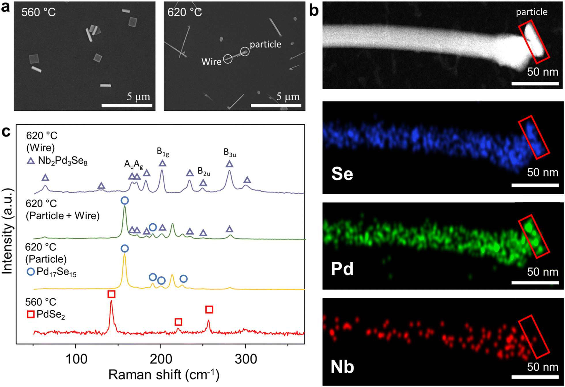 | ||
| Fig. 2 Growth of Nb2Pd3Se8 on SiO2. (a) SEM images of Nb2Pd3Se8 as grown at 560 and 620 °C (b) STEM-EDS mapping of Nb2Pd3Se8 grown at 620 °C, with the inset red rectangle highlighting the particle of Nb2Pd3Se8 (c) Raman spectra of grown at 560 and 620 °C. | ||
2.2 Characterization and device fabrication
Morphological analysis was conducted using field-emission scanning electron microscopy (FE-SEM; Hitachi, S-4300SE) at an accelerating voltage of 15 kV and a beam current of 10 μA.
All topographic analyses were performed in tapping mode using a Park system with Si cantilevers (≈300 kHz resonant frequency) coated with Al (Tap300 Al, Budget Sensors Inc.) at a scanning rate of ≈0.4 Hz. Aberration-corrected scanning transmission electron microscopy (STEM; JEOL, JEM-ARM200F) was performed at an acceleration voltage of 200 kV. Raman spectroscopy (LabRAM HR Evolution, HORIBA) was used to define the vibration modes of materials using a 785 nm laser.
3. Results and discussion
An aqueous precursor solution was prepared for the growth of Nb2Pd3Se8, which consists of a mixed solution of aqueous ammonium niobium oxalate (niobium precursor), aqueous ammonium tetrachloropalladate(II) (palladium precursor), and iodixanol. The precursor was mixed in a 2:3 molar ratio of Nb:Pd using a micropipette. The prepared precursor solution was coated on SiO2 using a spin coater, and calcination was performed. Fig. S2† illustrates the morphology of the precursors deposited on the substrate after calcination, showing uniformly deposited particles of approximately 10 nm in size. The number of particles increased with precursor concentration, indicating the controllability of the precursor. Subsequently, the substrate with the coated precursor was placed in an atmosphere-pressure CVD system, and Se was supplied during the experiment (Fig. 1b). As shown in Fig. 1c, Nb2Pd3Se8 wires were grown randomly on the substrate. Ribbon-shaped particles, as observed in the lattice structure, were arranged in a zigzag pattern, and each ribbon was formed in a tilted structure close to the (210) plane of the lattice.16,17 The Nb2Pd3Se8 grown on the substrate exhibited a strong preference peak at 14.43°, corresponding to the (210) plane of Nb2Pd3Se8 as observed through X-ray diffraction (Fig. 1d). According to the Wulff theorem, the shape of nanocrystals is determined by the surface energy of their crystallographic facets.41 This preferred peak can be attributed to the structural characteristics of the material. This preference is also seen in Nb2Pd3Se8 growth on the substrate. During the thermodynamic growth of nuclei, nanocrystals tend to grow faster on high-energy facets. For Nb2Pd3Se8, the (210) facet, like Ta2Pd3Se8, has high surface energy, resulting in faster growth rates along this facet, which manifests as the preferential appearance in PXRD.25 Therefore, the wires grow perpendicular to the substrate along the (210) facet, as shown in Fig. S3.† The SEM image illustrates nanowires growing attached to the substrate. (Fig. S3†) Raman spectroscopy revealed peaks at 166.7 (Au), 171.6 (Ag), 202.2 (B1g), 250.4 (B2u), and 301.2 (B3u) cm−1, which are similar to the calculated values for Nb2Pd3Se8 (Fig. 1e).19
In the CVD system, NbSe2 was synthesized at 800–850 °C.42,43 On the contrary, PdSe2 was synthesized between 300 and 550 °C.44,45 Nb2Pd3Se8 was synthesized at intermediate temperatures ranging from 600 to 800 °C in solid-state synthesis.13,17 In this experiment, synthesis was conducted in the CVD system at a temperature range of 570 to 730 °C, which is between the synthesis temperatures of PdSe2 and NbSe2. As shown in Fig. 2a and S4,† plate-shaped PdSe2 was synthesized at 570 °C, and wire formation was observed at 620 °C in some of the particles. Electron dispersion spectroscopy (EDS) mapping of the wires was performed to investigate the particle portion of the wires synthesized at 620 °C (Fig. 2b). The scanning transmission electron microscopy (STEM) EDS mapping data confirmed the presence of Nb, Pd, and Se compositions in the wires, whereas only Pd and Se compositions were observed in the particle portion. As shown in Fig. 2c, the nanoplates synthesized at 570 °C exhibited peaks at 145, 208, and 260 cm−1, corresponding to PdSe2.45–48 In the particle portion synthesized at 620 °C, Raman peaks at 157.7, 190, 213.5, and 226.3 cm−1, corresponding to Pd17Se15,48 were formed, whereas the wire portion showed peaks at 166.70, 171.5, 202.48, 250.35, and 301.2 cm−1, corresponding to Nb2Pd3Se8.19 Based on these Raman peaks observed, spectra simultaneously present in both the wire (Nb2Pd3Se8) and particle (Pd17Se15) portions suggest that these particles act as seeding promoters for Nb2Pd3Se8.
Experiments were conducted at 560, 580, 600, and 620 °C to determine the synthesis temperature of Nb2Pd3Se8 wires. Fig. 3a shows the temperature profile, where the temperature of the evaporation zone for the supply of Se was kept constant while the process temperature varied (experimental temperature was designed based on the phase diagram of Pd–Se shown in Fig. 3b). Fig. 3c displays SEM images corresponding to different synthesis temperatures. At 600 °C, only PdSe2 was formed, and Nb2Pd3Se8 did not synthesize. At 560, 580, and 600 °C, square-shaped PdSe2 was observed. At 620 °C, PdSe2 was not observed, and the growth of Nb2Pd3Se8 wires from Pd17Se15 was observed. As shown in phase diagram (Fig. 3b), the cause of this behaviour can be explained as follows: as the process temperature increases, the phase transition from PdSe2 to Pd17Se15 is induced during heating.47,48 Excessive Se, released during phase transition, contributes to the synthesis of Nb2Pd3Se8 wires.
 | ||
| Fig. 3 Effect of LPI-CVD process temperatures on synthesis. (a) Temperature profile of CVD synthesis. (b) Phase diagram illustrating the Pd–Se binary alloy system. (c) SEM images after the LPI-CVD process at temperatures 560, 580, 600 and 620 °C. | ||
Fig. 4a and b displays SEM images showing the synthesis of Nb2Pd3Se8 wires at different temperatures. The average lengths of the synthesized Nb2Pd3Se8 wires at 630, 650, and 670 °C are 2.29, 3.91, and 4.91 μm, respectively. In confirming reproducibility, four additional experiments were conducted at 670 °C, yielding wire lengths of 5.18, 4.89, 5.28, 4.91, and 4.53 μm. Length variations with temperature and the reproducibility results are presented in the histogram shown in Fig. 4c. At 690, 710, and 730 °C, Nb2Pd3Se8 wires were synthesized with average lengths of 11.55, 15.04, and 13.88 μm, respectively, and as a result, the aspect ratio was calculated with the increasing of process temperature. (See the ESI† Fig. S5). As shown in Pd–Se phase diagram (Fig. 3b), at temperatures above 680 °C, the Pd17Se15 phase cannot exist, and the observed growth was attributed to the partial growth in the liquid Se phase resulting from the rapid decomposition of PdSe2.47 However, at high process temperatures, a red shift was observed in the Raman spectra. Doped Nb2Pd3Se8 exhibited a red shift of 0.8 cm−1 compared with doped AuCl3 in previous research,19 whereas the B1g peak observed at 670, 690, and 710 °C showed significant shifts of 199.3, 197.7, and 195.29 cm−1, respectively (see the ESI† Fig. S6). This phenomenon is due to the loss of outermost Se atoms as shown in the thermogravimetric analysis (TGA) data above 480 °C.17 After processing at 650 °C, the loss of Se atoms from the outer region contributes to this phenomenon.
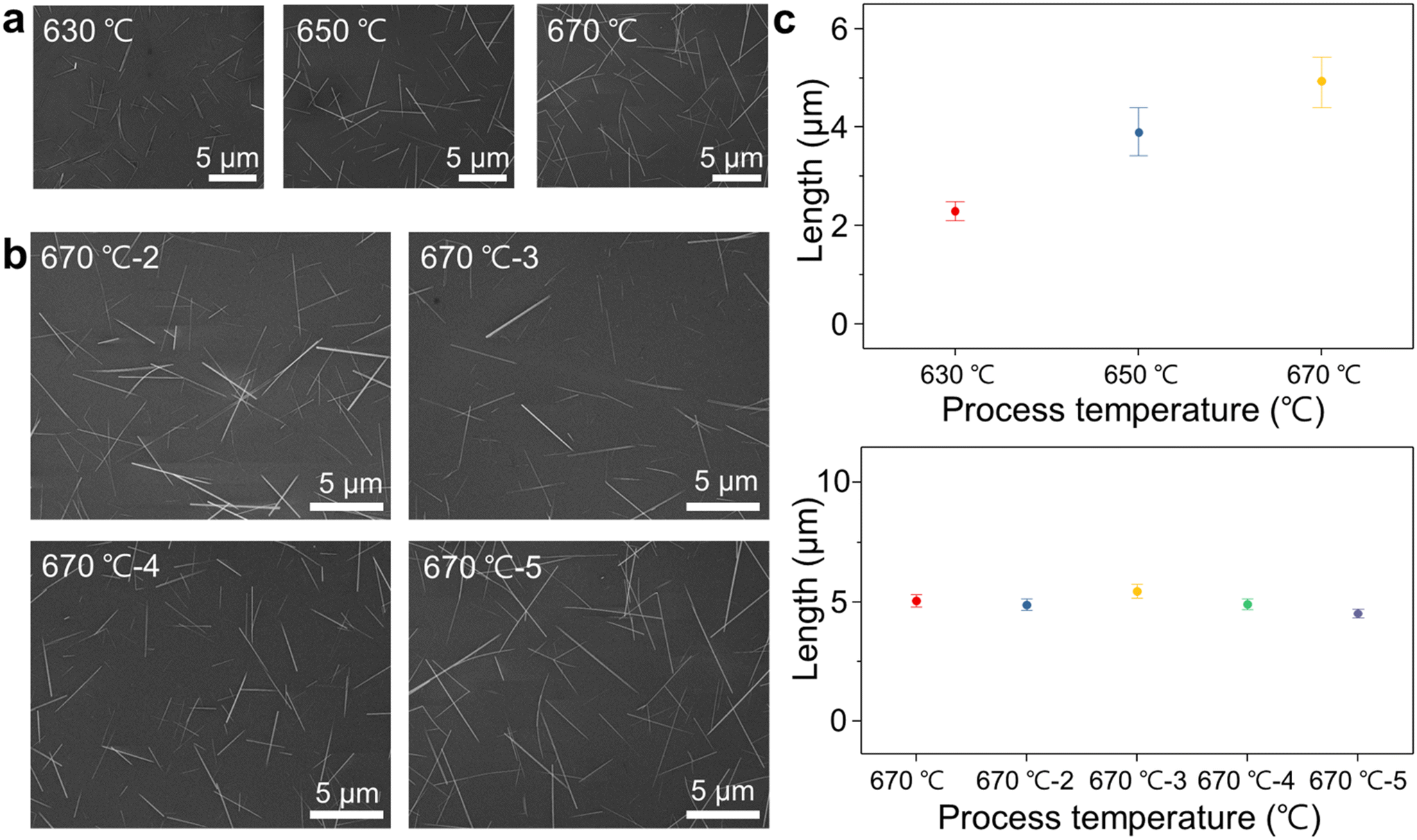 | ||
| Fig. 4 Growth of Nb2Pd3Se8 with various process temperatures. (a) SEM images of Nb2Pd3Se8 grown at 630, 650 and 670 °C. (b) Repetition results at 670 °C for four times. (c) Wire length dependent on process temperatures (top) and repetition experiments (bottom). | ||
STEM study was conducted on the synthesized Nb2Pd3Se8. The selected area electron diffraction (SAED) pattern shown in Fig. 5a indicates that the as synthesized wire is a single crystalline. High-resolution ADF-STEM images shown in Fig. 5b and c reveal the growth direction of the wire, which aligns with the (001) plane of Nb2Pd3Se8, corresponding to the chain direction. Furthermore, the outer direction of the wire corresponds to the (110) plane, with a distance of 8.87 Å.20Fig. 5d presents the EDS results obtained through STEM analysis, showing the presence of Nb, Pd, and Se. The Nb:Pd:Se ratio is determined to be 2:3.08:7.54, indicating Se deficiency. Moreover, the chemical bonding characteristics of Nb2Pd3Se8 nanowires were verified using X-ray photoelectron spectroscopy (XPS) in Fig. S6.† The XPS of Nb2Pd3Se8 grown on the substrate was examined. The binding energies for Nb 3d, Pd 3d, and Se 3d in the XPS of Nb2Pd3Se8 are as follows, the peaks observed at 204.7 and 207.4 eV correspond to Nb–Se 3d5/2 and Nb–Se 3d3/2. Peaks at 337.5 and 342.7 eV correspond to Pd 3d5/2 and Pd 3d3/2, and peaks at 54.4 and 55.2 eV correspond to Se 3d5/2 and Se 3d3/2 (Fig. S7†).41 Higher binding energy peaks of Nb 3d binding energy indicating Nb–O 3d5/2 and Nb–O 3d3/2 were detected, suggesting the presence of unreacted niobium oxide. The extracted atomic percentages for these peaks, excluding the niobium oxide energy peaks, align well with the STEM-EDS data ratios, with an atomic ratio of Nb/Pd/Se being 15.77:24.50:59.70 (2:3.10:7.56). This consistency supports the observed Se deficiency in the Nb2Pd3Se8 nanowires. This finding is consistent with Se deficiency observed in the TGA results of Nb2Pd3Se8, indicating the loss of Se after synthesis.
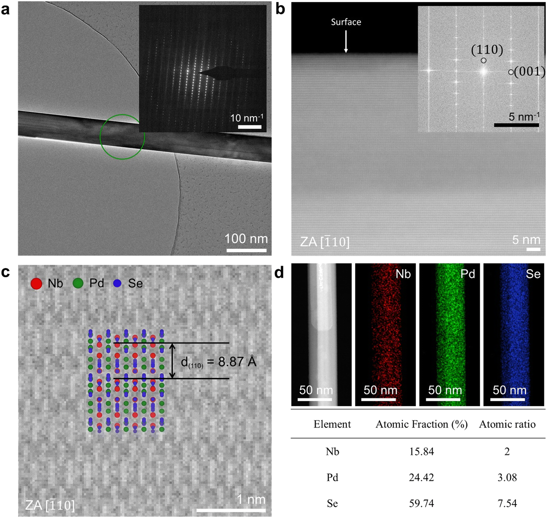 | ||
| Fig. 5 STEM study. HADDF-STEM: (a) low-magnification (inset image shows the SAED pattern) and (b) high-magnification image of Nb2Pd3Se8 (inset image shows the FFT pattern) (c) STEM images with zone axis [110] (d) EDS mapping data of Nb2Pd3Se8. | ||
A device shown in Fig. 6a was fabricated at a CVD process temperature of 630 °C to assess the quality of the synthesized Nb2Pd3Se8 for electronic devices. The FET device was produced by depositing Ti/Au on the CVD-grown Nb2Pd3Se8 using photolithography. In addition, the dimension of Nb2Pd3Se8 among the devices was examined using SEM and AFM (Fig. 6b and S8†). Fig. 6c presents the output curves (Ids–Vds) from −20 to 40 V, indicating the characteristics of an n-type semiconductor. In verifying the FET effect, transfer curves were measured by applying gate voltages (Vgs) ranging from −50 to 50 V at room temperature. The measured Ion/Ioff ratio was 575, and the threshold voltage was observed at −20 V. The field-effect mobility was calculated using the following formula;

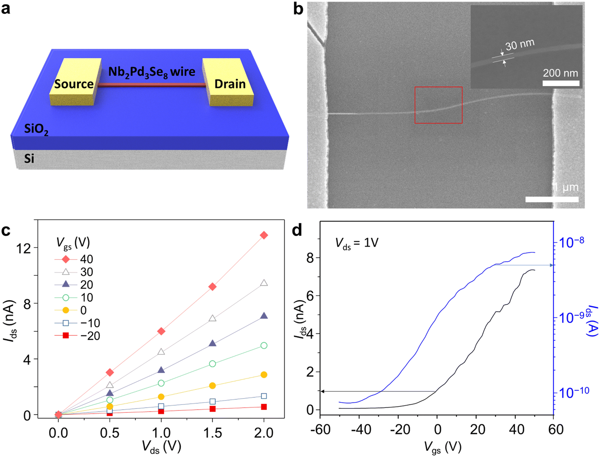 | ||
| Fig. 6 FET property of LPI-CVD-grown Nb2Pd3Se8. (a) Schematic of the Nb2Pd3Se8 electronic device. (b) SEM images of the device. Inset is the enlarged photo of the red bordered square area. (c) RT output characteristic (Ids–Vds) of Nb2Pd3Se8 FET under a gate bias ranging from −20 to 40 V. (d) RT transfer characteristic (Ids–Vgs) of Nb2Pd3Se8 FET under Vds of 1 V. | ||
4. Conclusions
In conclusion, we successfully synthesized Nb2Pd3Se8 wires, a ternary chalcogenide 1D van der Waals material, via liquid-phase intermediated chemical vapor deposition (LPI-CVD). By controlling the coating of Nb and Pd salts as precursors, we achieved the synthesis of Nb2Pd3Se8 wires with reproducible dimensions and electrical properties. Our results demonstrate the feasibility of synthesizing ternary systems beyond binary systems, indicating avenues for further exploration in diverse ternary phases. Moreover, the CVD synthesis of 1D van der Waals materials with semiconductor properties holds promise for integrated applications in nanomaterials and offers solutions applicable to mixed-dimensional studies. The characterization of Nb2Pd3Se8 wires through electron microscopy, spectroscopy, and device fabrication underscores its potential for electronic applications, as evidenced by the observed field-effect transistor behaviour and calculated electron mobility. Overall, our study contributes to the understanding and utilization of ternary chalcogenides in the realm of nanomaterials and electronics.Data availability
The data that support the findings of this study are available from the corresponding author, upon reasonable request.Author contributions
S. H. L. and B. J. J. contributed equally to this work. S. H. L. and B. J. J. were responsible for conceptualization, investigation, methodology, and writing – original draft. K. H. C., J. J., D. K., G. T. G., D. D. M. supported the analysis and investigation. S. C., B. L. and supported FET measurement. S. H. K., J. -Y. C. and H. K. Y. supervised the whole project.Conflicts of interest
There are no conflicts to declare.Acknowledgements
This research was supported by the Basic Science Research Program through the National Research Foundation of Korea, funded by the Korean government (MSIT, RS-2023-00208311). In addition, this work was supported by the KIST Institutional Program (Project No. 2E31854-22-066) from the Korea Institute of Science and Technology.References
- K. S. Novoselov, A. K. Geim, S. V. Morozov, D. Jiang, M. I. Katsnelson, I. V. Grigorieva, S. Dubonos and A. Firsov, Nature, 2005, 438, 197–200 CrossRef CAS PubMed.
- F. Xia, H. Wang and Y. Jia, Nat. Commun., 2014, 5, 4458 CrossRef CAS PubMed.
- S. Iijima and T. Ichihashi, Nature, 1993, 363, 603–605 CrossRef CAS.
- B. Radisavljevic, A. Radenovic, J. Brivio, V. Giacometti and A. Kis, Nat. Nanotechnol., 2011, 6, 147–150 CrossRef CAS PubMed.
- K. F. Mak, C. Lee, J. Hone, J. Shan and T. F. Heinz, Phys. Rev. Lett., 2010, 105, 136805 CrossRef PubMed.
- W. Liu, J. Kang, D. Sarkar, Y. Khatami, D. Jena and K. Banerjee, Nano Lett., 2013, 13, 1983–1990 CrossRef CAS PubMed.
- J. Wu, H. Yuan, M. Meng, C. Chen, Y. Sun, Z. Chen, W. Dang, C. Tan, Y. Liu and J. Yin, Nat. Nanotechnol., 2017, 12, 530–534 CrossRef CAS PubMed.
- Q. Liang, Y. Zheng, C. Du, Y. Luo, J. Zhang, B. Li, Y. Zong and Q. Yan, Small Methods, 2017, 1, 1700304 CrossRef.
- W. Chen, H. Chen, H. Zhu, Q. Gao, J. Luo, Y. Wang, S. Zhang, K. Zhang, C. Wang and Y. Xiong, Small, 2014, 10, 4637–4644 CrossRef CAS PubMed.
- Y. Lu, H. Kono, T. Larkin, A. Rost, T. Takayama, A. Boris, B. Keimer and H. Takagi, Nat. Commun., 2017, 8, 14408 CrossRef CAS PubMed.
- Y. Deng, Y. Yu, Y. Song, J. Zhang, N. Z. Wang, Z. Sun, Y. Yi, Y. Z. Wu, S. Wu and J. Zhu, Nature, 2018, 563, 94–99 CrossRef CAS PubMed.
- S. Cho, B. J. Jeong, K. H. Choi, B. Lee, J. Jeon, S. H. Lee, B. J. Kim, J. H. Lee, H. S. Oh and H. K. Yu, Small, 2022, 18, 2205344 CrossRef CAS PubMed.
- D. A. Keszler and J. A. Ibers, J. Solid State Chem., 1984, 52, 73–79 CrossRef CAS.
- K. H. Choi, B. J. Jeong, J. Jeon, Y. K. Chung, D. Sung, S. O. Yoon, S. Chae, B. J. Kim, S. Oh and S. H. Lee, Small, 2021, 17, 2102602 CrossRef CAS PubMed.
- B. J. Jeong, K. H. Choi, J. Jeon, S. O. Yoon, Y. K. Chung, D. Sung, S. Chae, S. Oh, B. J. Kim and S. H. Lee, Nanoscale, 2021, 13, 17945–17952 RSC.
- Q. Zhang, C. Liu, X. Liu, J. Liu, Z. Cui, Y. Zhang, L. Yang, Y. Zhao, T. T. Xu and Y. Chen, ACS Nano, 2018, 12, 2634–2642 CrossRef CAS PubMed.
- B. J. Jeong, K. H. Choi, J. Jeon, S. O. Yoon, Y. K. Chung, D. Sung, S. Chae, B. J. Kim, S. Oh and S. H. Lee, Adv. Funct. Mater., 2022, 32, 2108104 CrossRef CAS.
- M. Luo, T. Wu, S. Xu, R. Wang and F. Huang, Chem. Commun., 2022, 58, 6204–6207 RSC.
- B. J. Jeong, B. Lee, K. H. Choi, D. Sung, S. Ghods, J. Lee, J. Jeon, S. Cho, S. H. Lee and B. J. Kim, Nano Lett., 2023, 23, 6269–6275 CrossRef CAS PubMed.
- K. H. Choi, J. Jeon, B. J. Jeong, S. Chae, S. Oh, C. Woo, T. Y. Kim, J. Ahn, J. H. Lee and H. K. Yu, Adv. Mater. Interfaces, 2022, 9, 2200620 CrossRef CAS.
- A. A. Balandin, F. Kargar, T. T. Salguero and R. K. Lake, Mater. Today, 2022, 55, 74–91 CrossRef.
- Q. Qin, W. Gao, H. Zhang, J. Chen, Y. Yan, K. Zhu, M. Long, G. Li, S. Yin and Y. Du, J. Mater. Chem. A, 2023, 11, 11517–11525 RSC.
- P. Yang, S. Zhang, S. Pan, B. Tang, Y. Liang, X. Zhao, Z. Zhang, J. Shi, Y. Huan and Y. Shi, ACS Nano, 2020, 14, 5036–5045 CrossRef CAS PubMed.
- Z. Ma, S. Wang, Q. Deng, Z. Hou, X. Zhou, X. Li, F. Cui, H. Si, T. Zhai and H. Xu, Small, 2020, 16, 2000596 CrossRef CAS PubMed.
- Q. Zhang, X. Xiao, L. Li, D. Geng, W. Chen and W. Hu, Small, 2022, 18, 2107241 CrossRef CAS PubMed.
- R. Natsui, H. Shimizu, Y. Nakanishi, Z. Liu, A. Shimamura, N. T. Hung, Y.-C. Lin, T. Endo, J. Pu and I. Kikuchi, ACS Nano, 2023, 17, 5561–5569 CrossRef CAS PubMed.
- M. Sun, J. Li, Q. Ji, Y. Lin, J. Wang, C. Su, M.-H. Chiu, Y. Sun, H. Si and T. Palacios, Phys. Rev. Mater., 2021, 5, 094002 CrossRef CAS.
- H. E. Lim, Y. Nakanishi, Z. Liu, J. Pu, M. Maruyama, T. Endo, C. Ando, H. Shimizu, K. Yanagi and S. Okada, Nano Lett., 2020, 21, 243–249 CrossRef PubMed.
- Y. Yoo, J. S. Jeong, R. Ma, S. J. Koester and J. E. Johns, Chem. Mater., 2020, 32, 9650–9655 CrossRef CAS.
- J. Zhang, F. Wang, V. B. Shenoy, M. Tang and J. Lou, Mater. Today, 2020, 40, 132–139 CrossRef CAS.
- X. Ling, Y.-H. Lee, Y. Lin, W. Fang, L. Yu, M. S. Dresselhaus and J. Kong, Nano Lett., 2014, 14, 464–472 CrossRef CAS PubMed.
- L. Tang, T. Li, Y. Luo, S. Feng, Z. Cai, H. Zhang, B. Liu and H.-M. Cheng, ACS Nano, 2020, 14, 4646–4653 CrossRef CAS PubMed.
- G. H. Han, N. J. Kybert, C. H. Naylor, B. S. Lee, J. Ping, J. H. Park, J. Kang, S. Y. Lee, Y. H. Lee and R. Agarwal, Nat. Commun., 2015, 6, 6128 CrossRef CAS PubMed.
- J. Seo, J. Kim, J. Lee, D. Koo, G. Jeong, Y. Choi, E. B. Son and H. Park, Adv. Funct. Mater., 2022, 32, 2205695 CrossRef CAS.
- M. Kim, J. Seo, J. Kim, J. S. Moon, J. Lee, J.-H. Kim, J. Kang and H. Park, ACS Nano, 2021, 15, 3038–3046 CrossRef CAS PubMed.
- D. Jiang, X. Wang, R. Chen, J. Sun, H. Kang, D. Ji, Y. Liu and D. Wei, J. Am. Chem. Soc., 2022, 144, 8746–8755 CrossRef CAS PubMed.
- Q. Ji, C. Su, N. Mao, X. Tian, J.-C. Idrobo, J. Miao, W. A. Tisdale, A. Zettl, J. Li and J. Kong, Sci. Adv., 2021, 7, eabj3274 CrossRef CAS PubMed.
- J.-J. Tao, J. Jiang, S.-N. Zhao, Y. Zhang, X.-X. Li, X. Fang, P. Wang, W. Hu, Y. H. Lee and H.-L. Lu, ACS Nano, 2021, 15, 3241–3250 CrossRef CAS PubMed.
- W. Wang, Y. Meng, W. Wang, Z. Zhang, P. Xie, Z. Lai, X. Bu, Y. Li, C. Liu and Z. Yang, Adv. Funct. Mater., 2022, 32, 2203003 CrossRef CAS.
- H. Kim, Y. C. Kim, Y. H. Ahn and Y. Yoo, Chem. Eng. J., 2023, 468, 143678 CrossRef CAS.
- A. Giri, G. Park and U. Jeong, Chem. Rev., 2023, 123, 3329–3442 CrossRef CAS PubMed.
- S. Park, S. J. Yun, Y. I. Kim, J. H. Kim, Y.-M. Kim, K. K. Kim and Y. H. Lee, ACS Nano, 2020, 14, 8784–8792 CrossRef CAS PubMed.
- H. Wang, X. Huang, J. Lin, J. Cui, Y. Chen, C. Zhu, F. Liu, Q. Zeng, J. Zhou and P. Yu, Nat. Commun., 2017, 8, 394 CrossRef PubMed.
- Y. Gu, H. Cai, J. Dong, Y. Yu, A. N. Hoffman, C. Liu, A. D. Oyedele, Y. C. Lin, Z. Ge and A. A. Puretzky, Adv. Mater., 2020, 32, 1906238 CrossRef CAS PubMed.
- L.-S. Lu, G.-H. Chen, H.-Y. Cheng, C.-P. Chuu, K.-C. Lu, C.-H. Chen, M.-Y. Lu, T.-H. Chuang, D.-H. Wei and W.-C. Chueh, ACS Nano, 2020, 14, 4963–4972 CrossRef CAS PubMed.
- A. A. Puretzky, A. D. Oyedele, K. Xiao, A. V. Haglund, B. G. Sumpter, D. Mandrus, D. B. Geohegan and L. Liang, 2D Mater., 2018, 5, 035016 CrossRef.
- A. D. Oyedele, S. Yang, T. Feng, A. V. Haglund, Y. Gu, A. A. Puretzky, D. Briggs, C. M. Rouleau, M. F. Chisholm and R. R. Unocic, J. Am. Chem. Soc., 2019, 141, 8928–8936 CrossRef CAS PubMed.
- K. Ibrahim, K. C. Matthews, M. Coupin and J. H. Warner, Chem. Mater., 2022, 34, 9982–9988 CrossRef CAS.
Footnotes |
| † Electronic supplementary information (ESI) available. See DOI: https://doi.org/10.1039/d4ce00451e |
| ‡ These authors contributed equally. |
| This journal is © The Royal Society of Chemistry 2024 |