
 Open Access Article
 This Open Access Article is licensed under a
 Creative Commons Attribution 3.0 Unported Licence
Structure-directing synthesis of porous CuO–SiO2 nanocomposites using carbon nitride†
Yuki
Takeuchi
a,
Yasuhiro
Toyoda
b,
Kazuma
Gotoh
b and
Takahiro
Ohkubo
 *a
*a
aGraduate School of Natural Science and Technology, Okayama University, 3-1-1 Tsushimanaka, Kita-ku, Okayama 700-8530, Japan. E-mail: ohkubo@okayama-u.ac.jp; Tel: +81 86 251 7843
bCenter for Nano Materials and Technology, Japan Advanced Institute of Science and Technology (JAIST), 1-1 Asahidai, Nomi, Ishikawa 923-1292, Japan
First published on 7th May 2024
Abstract
Structure-directing synthesis, such as by the template method, allows us to control the porous structure and morphological properties of solid-state materials. Traditionally, molecules and zero-, one-, and three-dimensional materials have been used as structure-directing agents and templates. Recently, two-dimensional materials (e.g., graphene oxide and graphitic carbon nitride) have been investigated for their use in the synthesis of nanostructured materials. In this study, we used carbon nitride as the structure-directing agent for controlling SiO2 and cupric oxide (CuO) formation in the development of porous CuO–SiO2 nanocomposites via the calcination of a mixture of Cu2+, polyhedral oligomeric silsesquioxane (POSS), and carbon nitride to solve the problems with CuO (e.g., porosity control and low efficiency per weight relative to light materials). Further, we investigated the formation factors of the nanocomposites using comparative experiments to understand the roles of Cu2+, POSS, and carbon nitride. During calcination, carbon nitride induced the formation of SiO2, which supported CuO; the effect of Cu species removed carbon nitride. Subsequently, porous CuO–SiO2 nanocomposites were constructed. The constructed CuO–SiO2 nanocomposites presented a unique morphology (i.e., a fluffy structure), high surface area, and narrow optical band gap. The demonstrated method may pave the way for the design of CuO composite materials and the development of their application as adsorbents and catalysts.
Introduction
Transition metal oxides (TMOs) have long been studied for their unique electronic properties (i.e., various chemical valence states and band structures (conductivities)) and morphological characteristics.1 Among them, cupric oxide (CuO) is a p-type semiconductor with a band gap of 1.2–2.1 eV and catalytic properties.2–4 It has been employed in diverse applications, such as catalysts for H2 evolution3 and NO reduction with CO,5 sensors,6,7 adsorbents for CO2,8 and batteries (e.g., anode material for Li-ion batteries).9 However, TMOs suffer from low abundance (except for Fe), porosity control, and low efficiency per weight compared to materials comprising light elements, such as carbon and silica. To date, various fabrication techniques (e.g., sol–gel,10 pillaring,11 and combustion methods12) have been investigated, as well as the construction of composites with light materials (e.g., activated carbon13 and mesoporous silica14), for use in the fabrication of TMOs and their composites to achieve excellent porosity, to design targeted morphologies, and to reduce the use of transition metals.To control the porosity and morphology of the resulting materials, structure-directing synthesis such as the template method has been extensively studied in various solid-state materials, including mesoporous silica14–17 and zeolite-templated carbon.18,19 Mesoporous silica, which has aligned and size-controlled mesopores, was synthesized using surfactants (used as pore sources).14–17 Zeolite-templated carbon was synthesized using zeolite as the template, and it displayed an ordered micropore structure, a high surface area, and a single-layer graphene framework.18,19 Furthermore, nanostructured CuO was synthesized using a surfactant,12,20 a polycarbonate membrane,21 porous anodic alumina films,22 carbon nanotubes,23 carbon spheres,24 and Cu-based metal–organic frameworks25 as structure-directing agents and templates.
In addition to zero-, one-, and three-dimensional materials, two-dimensional materials have recently been actively investigated as templates. The synthesis of silica, silicon, metal, metal oxide (even CuO), transition metal dichalcogenide, and carbon nanosheets with controlled nanosheet size and thickness, unique structures, and superior porosity using graphene oxide and graphitic carbon nitride (g-C3N4) as templates has been proposed,26–36 and the construction of zeolites with nanopores generated by polymer-functionalized graphene oxide removal was reported.37 Furthermore, the construction of ultrathin amorphous metal oxide nanosheets using a lamellar Cu2O–oleate complex as a two-dimensional confining template has been demonstrated.38 Furthermore, composites such as Ni/CeO2,39 Mo2C–carbon,40 VN/nitrogen-doped carbon,41 and single-atom Fe/nitrogen-rich carbon42 were also fabricated using carbon nitride as a template. However, studies have not progressed on the use of carbon nitride to control the nanocomposite structure in CuO and SiO2, which have elemental abundance, low toxicity, and high thermal and chemical stability.27
In this study, porous CuO–SiO2 nanocomposites having a high specific surface area and unique morphologies were developed using a structure-directing synthesis to control the formation of CuO and SiO2. Polyhedral oligomeric silsesquioxane (POSS), in which Si and O are arranged in a cage structure, and carbon nitride were used as the SiO2 source and the structure-directing agent, respectively. We fabricated porous CuO–SiO2 nanocomposites via the calcination of a mixture of Cu2+, POSS, and carbon nitride (Scheme 1). We analyzed the properties of the porous CuO–SiO2 nanocomposites (e.g., their morphology and porosity), and we investigated the effects of Cu2+, POSS, and carbon nitride on the design and structure of the CuO–SiO2 nanocomposites.
 | ||
| Scheme 1 Construction of porous CuO–SiO2 nanocomposites using carbon nitride as the structure-directing agent. | ||
Experimental procedure
Materials
Urea was purchased from FUJIFILM Wako Pure Chemical Corporation, Japan. Octakis(tetramethylammonium) pentacyclo[9.5.1.13,9.15,15.17,13]octasiloxane-1,3,5,7,9,11,13,15-octakis(yloxide)hydrate (PSS, lot MKCL1508) was purchased from Sigma-Aldrich. Copper(II) acetate monohydrate (Cu(OAc)2·H2O) was purchased from Nacalai Tesque Inc., Japan. Distilled water was produced using a purification system (RFD240NA, ADVANTEC) and was used in all the experiments.Preparation of carbon nitride
Urea (30 g) was placed in a closed alumina box (the length, width, and height of the box were 70, 70, and 50 mm, respectively) and heated at 400 °C for 2 h (ramping rate: 3 °C min−1) in an air atmosphere. Subsequently, carbon nitride (U400) was obtained by naturally cooling the resultant product to room temperature.Synthesis of porous CuO–SiO2 nanocomposites
We added PSS (250, 500, 1500 mg) and Cu(OAc)2·H2O (350, 700, 2100 mg) to water (100 mL), where the ratio of PSS and Cu(OAc)2·H2O was fixed at 1![[thin space (1/6-em)]](https://www.rsc.org/images/entities/char_2009.gif) :8 (mol:mol) and PSS was assumed to contain no H2O, and we sonicated the mixture for 30 min. Next, we added U400 (1 g) to the dispersed water and sonicated the mixture for 30 min to disperse each material. Subsequently, we transferred the obtained dispersion to a container and heated it at 90 °C for 18 h (3 °C min−1) to evaporate the water. We then ground the dried powder at the bottom of the container (the intermediate product name up to this point in the process was U400/PSSx/Cu 90 °C, x: PSS amount). We placed U400/PSSx/Cu 90 °C in a closed alumina box and calcined it at 550 °C for 2 h (ramping rate: 3 °C min−1) in an air atmosphere. From this, we obtained porous CuO–SiO2 nanocomposites (U400/PSSx/Cu 550 °C).
:8 (mol:mol) and PSS was assumed to contain no H2O, and we sonicated the mixture for 30 min. Next, we added U400 (1 g) to the dispersed water and sonicated the mixture for 30 min to disperse each material. Subsequently, we transferred the obtained dispersion to a container and heated it at 90 °C for 18 h (3 °C min−1) to evaporate the water. We then ground the dried powder at the bottom of the container (the intermediate product name up to this point in the process was U400/PSSx/Cu 90 °C, x: PSS amount). We placed U400/PSSx/Cu 90 °C in a closed alumina box and calcined it at 550 °C for 2 h (ramping rate: 3 °C min−1) in an air atmosphere. From this, we obtained porous CuO–SiO2 nanocomposites (U400/PSSx/Cu 550 °C).
Synthesis of comparative samples
We synthesized comparative samples to investigate the role of each material based on the amounts of PSS (500 mg) and Cu(OAc)2·H2O (700 mg) without adding U400 (the intermediate product name was PSS/Cu 90 °C; the final product name was PSS/Cu 550 °C), PSS (the intermediate product name was U400/Cu 90 °C; the final product name was U400/Cu 550 °C), and Cu(OAc)2·H2O (the intermediate product name was U400/PSS 90 °C; the final product name was U400/PSS 550 °C), respectively. We obtained pristine CuO (Cu(OAc)2·H2O 550 °C) via the calcination of Cu(OAc)2·H2O at 550 °C for 2 h (ramping rate: 3 °C min−1) in an air atmosphere.We investigated the effect of calcination temperature using U400/PSS1500/Cu 90 °C. U400/PSS1500/Cu 90 °C was placed in a closed alumina box and calcined at 200 °C, 400 °C, and 550 °C (ramping rate: 3 °C min−1) in an air atmosphere without keeping the temperature. After the samples cooled naturally to room temperature, we obtained the comparative samples U400/PSS1500/Cu y °C (0 h) (y: calcination temperature).
Characterization
We carried out powder X-ray diffraction (XRD) using a MiniFlex II instrument (Rigaku Corporation, Japan) with monochromatic X-rays of Cu Kα (λ = 0.154 nm) at room temperature. The tube voltage, current, 2θ range, and step size were 30 kV, 15 mA, 5–60°, and 0.02°, respectively. We analyzed the states of C, N, Si, and Cu in the materials using X-ray photoelectron spectroscopy (XPS, JEOL JPS-9030, Japan). The X-ray source was Mg Kα (1253.6 eV). The path energies were 50 eV for the wide scans and 10 eV for the narrow scans. Carbon tape was used to fix the sample to the substrate (there is a possibility of carbon and silicone contamination.) Charge compensation was achieved using a flood gun. The binding energy of the C 1s peak at 284.8 eV was used as a reference to calibrate the binding energy scale. We obtained 29Si solid-state nuclear magnetic resonance (ssNMR) spectra using an Avance III NMR spectrometer (Bruker) with an 11.7 T magnet. We used a ϕ4 mm NMR sample rotor for magic angle spinning (MAS) measurements with an 8 kHz rotation. A single-pulse sequence with a 4.2 μs pulse was applied. We observed the morphologies of the samples by scanning electron microscopy (SEM, Keyence Corporation, Japan, VE-9800), and we captured the SEM images at an accelerating voltage of 5 kV. We measured the element ratios of Si and Cu using energy-dispersive X-ray spectroscopy (EDX, Keyence Corporation, Japan, 971863SP) and we used the average of ten measurements as the element ratio. We took transmission electron microscopy (TEM) and annular dark field scanning transmission electron microscopy (ADF-STEM)-EDX measurements using a JEM-ARM200F (JEOL, Japan). The TEM and STEM observations were performed at 200 kV. Using a BELSORP-mini instrument (MicrotracBEL Corp., Japan), we evaluated the porous structure. We performed N2 adsorption–desorption tests at 77 K to obtain the adsorption–desorption isotherms of the samples. All the samples were evacuated at 150 °C for 3 h before the measurements. We analyzed the isotherms using the Brunauer–Emmett–Teller (BET) equation to determine the specific surface area of the samples. We analyzed the adsorption isotherm using the Barrett, Joyner, and Halenda (BJH) method to obtain the pore size distribution. We obtained ultraviolet-visible (UV-vis) spectra using a Jasco V-770 spectrophotometer (Jasco, Japan) for UV-vis diffuse reflectance spectroscopy over a wavelength range of 200–1200nm.
CO2 adsorption test
We conducted CO2 adsorption tests using a BELSORP-max (MicrotracBEL Corp., Japan) at 303 K. The sample was evacuated at 110 °C for 12 h before measurement.Results and discussion
Synthesis of porous CuO–SiO2 nanocomposites
We synthesized porous CuO–SiO2 nanocomposites (U400/PSSx/Cu 550 °C) by calcining a mixture of Cu2+, POSS, and U400 using the POSS–tetramethylammonium complex (PSS) as the SiO2 source and carbon nitride as the structure-directing agent. First, we prepared U400 by heating urea at 400 °C. The crystalline structures were analyzed with XRD. The peaks observed in the XRD pattern of U400 were different from those of urea, which suggests the conversion of urea (Fig. S1†). The XRD pattern of U400 was similar to that previously reported.43 Its peak positions were relatively close to those of g-C3N4 (27.4° (002) and 13.0° (100)),44 which suggests that the g-C3N4 intermediate (carbon nitride) was constructed. We confirmed the element states of U400 using XPS (Fig. S2†). The XPS survey scan (Fig. S2a†) showed the presence of C and N derived from carbon nitride in U400. In the C 1s region (Fig. S2b†), there were two peaks derived from the adventitious hydrocarbon of the XPS instrument itself and defect-containing sp2-hybridized carbon atoms in the graphitic domains (284.8 eV) and C–N–C (288.3 eV).45 The peak in the N 1s region was deconvoluted to three components: neutral imine (398.6 eV), neutral amine (399.3 eV), and positively charged N species (400.4 eV) (Fig. S2c†).46 Second, we prepared a mixture of Cu2+ and POSS (PSS/Cu). We confirmed the PSS/Cu states by analyzing the crystalline structure of PSS/Cu 90 °C, which was synthesized by drying the mixture of PSS and Cu(OAc)2·H2O in water, using XRD. The XRD pattern for PSS/Cu 90 °C is shown in Fig. 1 and S3.† In PSS/Cu 90 °C, we detected a peak at 2θ = 11.5°, which was not found in PSS or Cu(OAc)2·H2O (Fig. S3†); this suggests that structural changes in PSS and Cu(OAc)2·H2O occurred during the mixing or drying process. Third, we prepared a mixture of Cu2+, POSS, and U400 (U400/PSSx/Cu 90 °C) by mixing U400 with Cu2+/POSS-dispersed water and evaporating water in the U400/Cu2+/POSS-containing water. The XRD pattern of U400/PSS250/Cu 90 °C was similar to that of U400 (Fig. 1). However, the peak at 2θ = 9.3° was confirmed in U400/PSS250/Cu 90 °C which was not found in U400 or PSS/Cu 90 °C (Fig. 1). Further, in U400/PSS1500/Cu 90 °C, peaks such as between 14° and 17° as well as around 25°, which were not confirmed in U400/PSS250/Cu 90 °C and U400/PSS500/Cu 90 °C, were observed (Fig. S4†). These facile peaks and changes of patterns might have been due to the structural changes in U400, Cu2+, or POSS when they were combined during the fabrication of U400/PSSx/Cu 90 °C and the concentration differences of Cu2+/POSS in the U400/Cu2+/POSS mixtures. | ||
| Fig. 1 XRD patterns for U400, PSS/Cu 90 °C, and U400/PSS250/Cu 90 °C. | ||
Next, we constructed porous CuO–SiO2 nanocomposites (U400/PSSx/Cu 550 °C) via the calcination of the obtained intermediates (U400/PSSx/Cu 90 °C) at 550 °C in an air atmosphere. The formation of CuO and SiO2, and the removal of carbon nitride were confirmed by XRD and XPS. According to the XRD patterns of U400/PSSx/Cu 550 °C (Fig. 2a and S5†), peaks that were attributed to CuO47 were detected, and the XRD patterns were similar to that of Cu(OAc)2·H2O 550 °C, which was synthesized via the heating of Cu(OAc)2·H2O at 550 °C in an air atmosphere. This pattern similarity suggests that CuO was formed by calcining U400/PSSx/Cu 90 °C. The intensity of the peak at 36° was higher than that at 39° in U400/PSSx/Cu 550 °C; the tendency of intensities was opposite to that of Cu(OAc)2·H2O 550 °C, which suggests that the crystal growth of CuO was directed by carbon nitride and/or PSS(-derived SiO2). Furthermore, the widths at half-maximum intensity of the peaks at 36° were 0.32° in U400/PSS250/Cu 550 °C and 0.29° in Cu(OAc)2·H2O 550 °C; those at 39° in U400/PSS250/Cu 550 °C and Cu(OAc)2·H2O were 0.41 and 0.31°, respectively (Table S1†). In comparing U400/PSS250/Cu 550 °C with Cu(OAc)2·H2O 550 °C, we observed that the widths at 36° were similar; however, the width at 39° in U400/PSS250/Cu 550 °C was wider than that in Cu(OAc)2·H2O 550 °C. According to the Scherrer equation (Dhkl = Kλ/Bcosθ, where Dhkl is the length of the crystallite in the direction perpendicular to the lattice planes (hkl), K is the Scherrer constant, λ is the wavelength of the X-rays, B is the corrected band broadening after the subtraction of the equipment broadening, and θ is half the diffraction angle48–50), when B increases, Dhkl decreases, which indicates that D111,200 in U400/PSS250/Cu 550 °C was smaller than that in Cu(OAc)2·H2O 550 °C. These XRD results suggest that the crystal growth in the direction perpendicular to the (111, 200) planes was suppressed in U400/PSS250(x)/Cu 550 °C relative to that in Cu(OAc)2·H2O 550 °C. We confirmed the element states using XPS (Fig. 2b and c and S6–S8†). The survey scans showed that C, N, O, Si, and Cu were detected in U400/PSS250/Cu 90 °C and that C, O, Si, and Cu were detected in U400/PSS250/Cu 550 °C (Fig. S6†). The results of the Cu 2p region (Fig. 2b) showed that satellite peaks (940–946 eV and 960–965 eV) derived from Cu2+ (CuO) were present in U400/PSS250/Cu 550 °C.51 The Auger parameters were calculated using the Cu 2p3/2 photoelectron peaks (Fig. 2b) and Cu L3M4,5M4,5 Auger peaks (Fig. S7†).52,53 The Auger parameters (Table S2†) for Cu(OAc)2·H2O 550 °C (1851.6 eV) and for U400/PSS250/Cu 550 °C (1851.8 eV) were close to that for CuO (1851.5 eV) but not to that for Cu2O (1849.2 eV),53 which supports the XRD results and CuO formation. We verified carbon nitride removal using the spectra in the N 1s region (Fig. 2c). The comparison between the spectra for U400/PSS250/Cu 90 °C and those for U400/PSS250/Cu 550 °C showed that although the peak derived from carbon nitride was confirmed in U400/PSS250/Cu 90 °C, this peak was not detected in U400/PSS250/Cu 550 °C, which suggests that the N (carbon nitride) removal occurred during calcination. We analyzed SiO2 formation using 29Si MAS NMR and XPS. Two SiO2 components were observed in the 29Si MAS NMR spectrum for U400/PSS250/Cu 550 °C (Fig. 2d): a main component at −112 ppm and a shoulder structure at −102 ppm, which were assigned to the Q4 and Q3 sites of the SiO4 structure, respectively.54,55 The Q4 and Q3 ratio was estimated to be 4.9:1, which suggests that fully condensed sites were abundant; this would support SiO2 formation. The XPS spectra in the Si 2p region are shown in Fig. S8.† Si peaks were detected for both U400/PSS250/Cu 90 °C and U400/PSS250/Cu 550 °C; however, their peak positions were different. Compared with the peak position of U400/PSS250/Cu 90 °C (102.3 eV), the peak position of U400/PSS250/Cu 550 °C (104.2 eV) was shifted to a higher binding energy. Kaur et al. reported that the peaks at 102.7 eV and 103.7 eV corresponded to Si–O (and Si–O–C) bonds and SiO2, respectively,56 which suggests that SiO2 formation was induced by calcination at 550 °C for 2 h. We performed EDX to obtain the Si and Cu ratios, and we present the results in Tables S3–S5.† The Si and Cu element ratios in U400/PSS250/Cu 550 °C, U400/PSS500/Cu 550 °C, and U400/PSS1500/Cu 550 °C were 46:54, 37:63, and 48:52, respectively; the values of U400/PSSx/Cu 550 °C were relatively close. The experimental yields of U400/PSS250/Cu 550 °C, U400/PSS500/Cu 550 °C, and U400/PSS1500/Cu 550 °C were 11.7, 19.3, and 30.3%, respectively; the experimental yields were similar to the theoretical yields of CuO and SiO2 (Table S6†), which suggests that U400/PSSx/Cu 550 °C mainly contained CuO and SiO2. According to the XRD patterns, XPS spectra, and the Si and Cu element ratios, the CuO–SiO2 nanocomposites were fabricated via the calcination of U400/Cu2+/POSS mixtures (U400/PSSx/Cu 90 °C), thereby inducing the formation of SiO2 and CuO as well as carbon nitride removal.
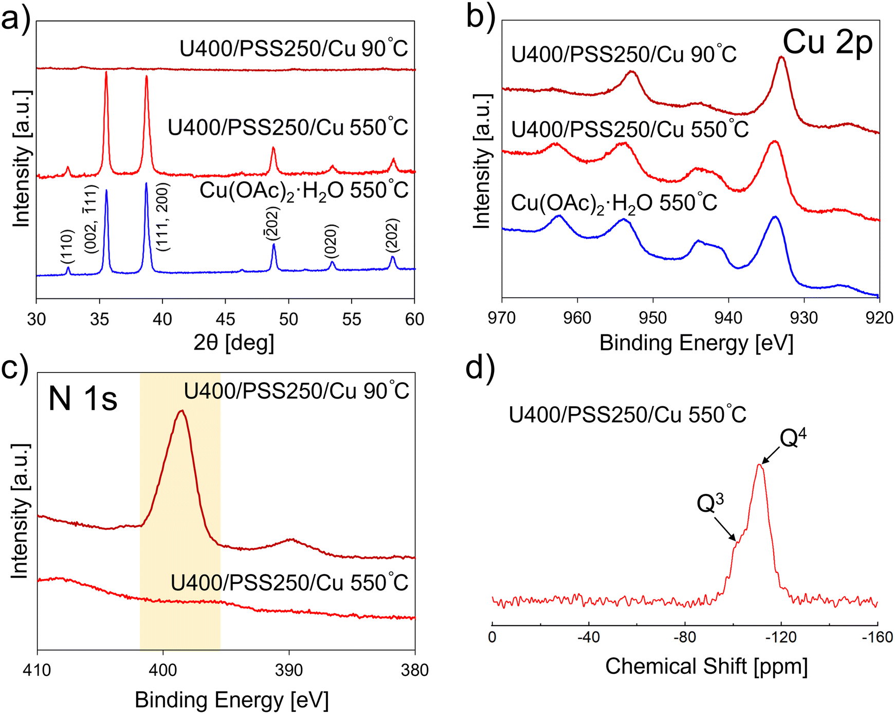 | ||
| Fig. 2 a) XRD patterns for U400/PSS250/Cu 90 °C, U400/PSS250/Cu 550 °C, and Cu(OAc)2·H2O 550 °C. High-resolution XPS spectra for b) the Cu 2p region for U400/PSS250/Cu 90 °C, U400/PSS250/Cu 550 °C, and Cu(OAc)2·H2O 550 °C and c) the N 1s region for U400/PSS250/Cu 90 °C and U400/PSS250/Cu 550 °C. d) 29Si MAS NMR spectrum for U400/PSS250/Cu 550 °C. | ||
We analyzed the morphologies of the CuO–SiO2 nanocomposites via SEM. The SEM images of U400/PSSx/Cu 550 °C are shown in Fig. 3. U400/PSSx/Cu 550 °C had a fluffy structure. We obtained the microstructure and elemental mapping using TEM and STEM-EDX measurements (Fig. 4). The TEM and STEM images and EDX elemental mappings for U400/PSS250/Cu 550 °C and U400/PSS1500/Cu 550 °C suggest that the SiO2 had a fluffy structure and that the SiO2 supported CuO. The preferential formation of fluffy SiO2 might have been due to a possible number of interactions between carbon nitride and the precursors of SiO2 and CuO (PSS and Cu(OAc)2·H2O). It is presumed that POSS in PSS had a greater number of interactions with U400 per molecule than did Cu(OAc)2·H2O, which suggests that PSS was greatly influenced by the structure-directing effect of U400.
 | ||
| Fig. 3 SEM images of U400/PSS250/Cu 550 °C (a and d), U400/PSS500/Cu 550 °C (b and e), and U400/PSS1500/Cu 550 °C (c and f). | ||
 | ||
| Fig. 4 TEM images of U400/PSS250/Cu 550 °C (a) and U400/PSS1500/Cu 550 °C (e). STEM images and EDX elemental mappings of U400/PSS250/Cu 550 °C (b–d) and U400/PSS1500/Cu 550 °C (f–h). | ||
We measured the porosity of the CuO–SiO2 nanocomposites using N2 adsorption–desorption tests, and we show the N2 adsorption–desorption isotherms in Fig. 5a and S9.† The isotherm types for U400/PSSx/Cu 550 °C were assigned to type IV(a), which represents the presence of mesopores.57 In addition, according to the isotherms and pore size distributions we obtained using the BJH method (Fig. S10†), U400/PSSx/Cu 550 °C had a pore structure comprising micropores and small mesopores (<10 nm). The specific surface areas (SBET) of U400/PSS250/Cu 550 °C, U400/PSS500/Cu 550 °C, and U400/PSS1500/Cu 550 °C were 157, 153, and 214 m2 g−1, respectively (Table S7†). The SBET of U400/PSS1500/Cu 550 °C was higher than those of U400/PSS250/Cu 550 °C and U400/PSS500/Cu 550 °C. This difference in SBET might have been due to the increase in the concentration of Cu2+/POSS in the U400/Cu2+/POSS mixtures or to the structural differences in the U400/Cu2+/POSS mixtures (U400/PSSx/Cu 90 °C), as confirmed by XRD (Fig. S4†). Furthermore, U400/PSSx/Cu 550 °C had a higher specific surface area than did Cu(OAc)2·H2O 550 °C (1 m2 g−1). Compared with porous CuO and CuO–SiO2 composites in previous research (which have shown high Cu and CuO contents (>25 wt%)) (Table S8†),20,24,25,58–63 the developed U400/PSSx/Cu 550 °C had a relatively higher specific surface area.
 | ||
| Fig. 5 a) N2 adsorption–desorption isotherms and b) UV-vis absorption spectra of U400/PSS500/Cu 550 °C, U400/PSS1500/Cu 550 °C, and Cu(OAc)2·H2O 550 °C. | ||
We analyzed the optical properties (band gaps) of the nanocomposites using UV-vis absorption spectra. As shown in Fig. 5b, U400/PSS500/Cu 550 °C and U400/PSS1500/Cu 550 °C had high visible-light absorption and similar spectra; the shapes of their spectra were similar to those of Cu(OAc)2·H2O 550 °C (pristine CuO). We calculated the optical band gaps using the Tauc approach (Fig. S11†), [F(R∞)hν]n = A (hν − Eg), where A is a constant, n is a coefficient (n = 1/2 for the materials with an indirect band gap; n = 2 for the materials with a direct band gap), h is the Planck constant, ν is the photon frequency rate, Eg is the band gap, and F(R∞) is the Kubelka–Munk function.64,65 The band gaps of U400/PSS500/Cu 550 °C and U400/PSS1500/Cu 550 °C were 1.32 eV and 1.31 eV, respectively, which were close to that of Cu(OAc)2·H2O 550 °C (1.24 eV). The slight increases in the band gaps in U400/PSSx/Cu 550 °C might have been due to the introduction of SiO2 or to differences in the crystal growth of CuO. Owing to the results of SEM, the N2 adsorption–desorption tests, and the UV-is absorption spectra, we constructed porous CuO–SiO2 nanocomposites having unique morphologies (e.g., fluffy structures), high surface areas, and narrow optical band gaps. According to the literature (Table S9†),66–70 the band gap values of U400/PSSx/Cu 550 °C were close to those of other CuO composite materials.
The synthesized CuO–SiO2 nanocomposites can be used in adsorption–separation applications and as catalysts because of their unique morphologies, high specific surface areas, and narrow band gaps. We performed CO2 adsorption tests at 303 K. The isotherms are shown in Fig. 6. Compared with the CO2 uptake of Cu(OAc)2·H2O 550 °C (0.0056 mmol g−1), that of U400/PSS1500/Cu 550 °C (0.21 mmol g−1) was enhanced, which was due to the improved porosity, suggesting improved performance in applications for CO2 capture and/or utilization.
 | ||
| Fig. 6 CO2 adsorption isotherms of U400/PSS1500/Cu 550 °C and Cu(OAc)2·H2O 550 °C. | ||
Elucidation of the formation factors
We elucidated the formation factors of porous CuO–SiO2 nanocomposites using comparative experiments to investigate the roles of Cu2+, POSS, and carbon nitride. Here, we first discuss SiO2 formation. The Si and Cu ratios in porous CuO–SiO2 nanocomposites (U400/PSSx/Cu 550 °C) were almost 1:1 (Tables S3–S5†). However, PSS/Cu 550 °C, which was prepared without adding U400, had a lower Si ratio than did U400/PSSx/Cu 550 °C (Table S10†); this difference suggests that carbon nitride suppressed the removal of POSS and induced SiO2 formation. Second, we investigated the removal of carbon nitride using U400/Cu 550 °C, which was prepared without adding PSS, and U400/PSS 550 °C, which was prepared without adding Cu(OAc)2·H2O. U400/Cu 550 °C did not show a peak around 399 eV (Fig. S12a†), and the peak derived from carbon nitride remained for U400/PSS 550 °C (Fig. S12b†). These results suggest that the Cu species induced the removal of N (carbon nitride). Third, we examined the factors determining morphology and porosity. From the SEM images, rigid structures were confirmed in PSS/Cu 550 °C, U400/Cu 550 °C, and Cu(OAc)2·H2O 550 °C, whereas fluffy structures, which were observed in U400/PSSx/Cu 550 °C, were not observed (Fig. 7 and S13†). Furthermore, in terms of porosity, the N2-adsorbed volume of U400/Cu 550 °C (Fig. S14†) was extremely small compared with that of U400/PSSx/Cu 550 °C, which suggests that the SiO2 formation process induced by carbon nitride played an important role in the enhancement of the porosity in U400/PSSx/Cu 550 °C. According to the results of the EDX, SEM, and N2 adsorption–desorption tests, porous CuO–SiO2 nanocomposites having a fluffy structure and high surface areas were constructed owing to the formation process of SiO2, which supported CuO, induced by carbon nitride rather than by the individual effects of U400 and PSS. Finally, we investigated the effects of calcination temperature. According to the Cu 2p region (Fig. S15a†), the peak shape (peak position and satellite peaks (940–946 eV and 960–965 eV) derived from Cu2+ (CuO)) for the samples after calcination at temperatures greater than 400 °C was similar to that of U400/PSS1500/Cu 550 °C, which suggests that CuO was formed between 200 °C and 400 °C. In the N 1s region (Fig. S15b†), the peak derived from carbon nitride disappeared completely in U400/PSS1500/Cu 550 °C (0 h) after CuO was formed. In addition, as the calcination temperature increased, the peak positions in the Si 2p region (Fig. S15c†) gradually shifted toward a higher binding energy, which suggests that SiO2 formation occurred gradually while the temperature rose to and stabilized at 550 °C. According to these results, the proposed formation processes of fluffy porous CuO–SiO2 nanocomposites can be described as follows:
 | ||
| Fig. 7 SEM images of U400/Cu 550 °C (a and d), PSS/Cu 550 °C (b and e), and U400/PSS500/Cu 550 °C, in which the location was different from Fig. 3b and e (c and f). | ||
a) Carbon nitride suppressed the removal of POSS and induced SiO2 formation, and the fluffy SiO2 supported CuO.
b) Carbon nitride was removed by the effect of Cu species (e.g., CuO) during calcination, and fluffy porous CuO–SiO2 nanocomposites were synthesized.
In this study, fluffy porous CuO–SiO2 nanocomposites were developed by controlling CuO and SiO2 formation using carbon nitride as the structure-directing agent. Two-dimensional materials have previously been used as templates for various materials (e.g., SiO2 and metal oxide).27,28,31–33 However, with the method used in this study, carbon nitride was not able to control the CuO structure (morphology and porosity) by itself; the SiO2 formation process induced by carbon nitride controlled the structure of CuO by supporting it with formed SiO2, and fluffy porous CuO–SiO2 nanocomposites were fabricated. This study suggests that the synthesis method that uses the SiO2 formation process induced by carbon nitride (two-dimensional materials) in the presence of a precursor may control the structure of materials that cannot be controlled by two-dimensional materials alone (although the SiO2 remains in the product). Further, in the synthesis process, the method in this study concurrently induced the CuO and SiO2 formation. The synthesis method simultaneously forming CuO and SiO2 may be possible to reduce the number of steps of substance formation compared to the two-step formation processes such as modification of CuO after the synthesis of porous silica. This study contributes to the exploration of structural control and synthesis technology in solid-state materials.
Conclusions
We developed porous CuO–SiO2 nanocomposites having high surface areas and unique morphologies by calcining a mixture of Cu2+, POSS, and carbon nitride, which was used as a structure-directing agent to control the structure of the CuO–SiO2 nanocomposites. Carbon nitride suppressed POSS removal and induced SiO2 formation in the porous CuO–SiO2 nanocomposites, and the formed SiO2 had a fluffy structure and supported CuO. Carbon nitride was removed by the effect of Cu species (e.g., CuO), and porous CuO–SiO2 nanocomposites were developed. Changing the Cu2+/POSS mixture to carbon nitride ratio in the Cu2+/POSS/carbon nitride mixture changed the porosity of the porous CuO–SiO2 nanocomposites. The synthesized porous CuO–SiO2 nanocomposites with narrow optical band gaps have potential for application as adsorbents and catalysts. The constructed materials and the proposed synthesis method may contribute to the development of porous materials and their applications as adsorbents and catalysts.Author contributions
Yuki Takeuchi: conceptualization; data curation; formal analysis; funding acquisition; validation; methodology; investigation; visualization; writing – original draft; writing – review & editing. Yasuhiro Toyoda: investigation; writing – review & editing. Kazuma Gotoh: investigation; visualization; writing – review & editing. Takahiro Ohkubo: resources; supervision; writing – review & editing; project administration.Conflicts of interest
There are no conflicts to declare.Acknowledgements
The authors would like to express their gratitude to Prof. Tatsuo Fujii (Okayama University) and his group members for the support in using BELSORP-mini. The authors also thank Prof. Takashi Kambe (Okayama University) and his group members for their support in using SEM–EDX. The authors appreciate Dr. Chiyuu Nakano (Okayama University) for conducting the entrusted measurement of XPS. The TEM and STEM-EDX measurements were supported by “Advanced Research Infrastructure for Materials and Nanotechnology in Japan (ARIM)” of the Ministry of Education, Culture, Sports, Science and Technology (MEXT) under Grant Number JPMXP1223JI0054.This work was supported by JST, the establishment of university fellowships towards the creation of science technology innovation, Grant Number JPMJFS2128. Y. Takeuchi would like to express their deepest gratitude to the Public Interest Incorporated Foundation “Ohmoto Ikueikai” for their generous financial support over the past 3 years in carrying out this research.
References
- M. Zheng, H. Tang, L. Li, Q. Hu, L. Zhang, H. Xue and H. Pang, Adv. Sci., 2018, 5, 1700592 CrossRef PubMed.
- Z. S. Fishman, B. Rudshteyn, Y. He, B. Liu, S. Chaudhuri, M. Askerka, G. L. Haller, V. S. Batista and L. D. Pfefferle, J. Am. Chem. Soc., 2016, 138, 10978–10985 CrossRef CAS PubMed.
- F. Wang, L. Xiao, J. Chen, L. Chen, R. Fang and Y. Li, ChemSusChem, 2020, 13, 5711–5721 CrossRef CAS PubMed.
- X. Xu, H. Yang and Y. Liu, CrystEngComm, 2012, 14, 5289–5298 RSC.
- A. Patel, T. E. Rufford, V. Rudolph and Z. Zhu, Catal. Today, 2011, 166, 188–193 CrossRef CAS.
- J. Zhang, J. Liu, Q. Peng, X. Wang and Y. Li, Chem. Mater., 2006, 18, 867–871 CrossRef CAS.
- X. Zhang, G. Wang, X. Liu, J. Wu, M. Li, J. Gu, H. Liu and B. Fang, J. Phys. Chem. C, 2008, 112, 16845–16849 CrossRef CAS.
- W. N. R. Wan Isahak, Z. A. Che Ramli, W. Z. Samad and M. A. Yarmo, J. Teknol., 2015, 77, 105–114 Search PubMed.
- S. Ko, J.-I. Lee, H. S. Yang, S. Park and U. Jeong, Adv. Mater., 2012, 24, 4451–4456 CrossRef CAS PubMed.
- D. J. Suh and T.-J. Park, Chem. Mater., 1996, 8, 509–513 CrossRef CAS.
- M. W. Anderson and J. Klinowski, Inorg. Chem., 1990, 29, 3260–3263 CrossRef CAS.
- C. Dong, X. Xiao, G. Chen, H. Guan and Y. Wang, Appl. Surf. Sci., 2015, 349, 844–848 CrossRef CAS.
- C. Boruban and E. N. Esenturk, J. Nanopart. Res., 2018, 20, 59 CrossRef.
- Z. Li and L. Gao, J. Phys. Chem. Solids, 2003, 64, 223–228 CrossRef CAS.
- C. T. Kresge, M. E. Leonowicz, W. J. Roth, J. C. Vartuli and J. S. Beck, Nature, 1992, 359, 710–712 CrossRef CAS.
- D. Zhao, Q. Huo, J. Feng, B. F. Chmelka and G. D. Stucky, J. Am. Chem. Soc., 1998, 120, 6024–6036 CrossRef CAS.
- A. B. D. Nandiyanto, S.-G. Kim, F. Iskandar and K. Okuyama, Microporous Mesoporous Mater., 2009, 120, 447–453 CrossRef CAS.
- T. Kyotani, T. Nagai, S. Inoue and A. Tomita, Chem. Mater., 1997, 9, 609–615 CrossRef CAS.
- H. Nishihara and T. Kyotani, Chem. Commun., 2018, 54, 5648–5673 RSC.
- G. S. Gund, D. P. Dubal, D. S. Dhawale, S. S. Shinde and C. D. Lokhande, RSC Adv., 2013, 3, 24099–24107 RSC.
- X. Li, Y. Wang, Y. Lei and Z. Gu, RSC Adv., 2012, 2, 2302–2307 RSC.
- Y. F. Zhu, G. H. Zhou, Y. B. Lin and L. Liu, Cryst. Res. Technol., 2012, 47, 658–662 CrossRef CAS.
- H.-Q. Wu, X.-W. Wei, M.-W. Shao, J.-S. Gu and M.-Z. Qu, Chem. Phys. Lett., 2002, 364, 152–156 CrossRef CAS.
- Q. Shao, X. Wang, Q. Liu, L. Wang, C. Kang, Q. Wang and S. Ge, J. Nanosci. Nanotechnol., 2011, 11, 10271–10277 CrossRef CAS PubMed.
- K. Kim, P. G. Choi, T. Itoh and Y. Masuda, Adv. Mater. Interfaces, 2021, 8, 2100283 CrossRef CAS.
- L. Kou and C. Gao, Nanoscale, 2011, 3, 519–528 RSC.
- B. K. Birdsong, B. W. Hoogendoorn, F. Nilsson, R. L. Andersson, A. J. Capezza, M. S. Hedenqvist, S. Farris, A. Guerrero and R. T. Olsson, Nanoscale, 2023, 15, 13037–13048 RSC.
- Z. Shen, Q. Cai, C. Yin, Q. Xia, J. Cheng, X. Li and Y. Wang, Chem. Eng. Sci., 2020, 217, 115528 CrossRef CAS.
- Z. Lu, J. Zhu, D. Sim, W. Zhou, W. Shi, H. H. Hng and Q. Yan, Chem. Mater., 2011, 23, 5293–5295 CrossRef CAS.
- S. Takenaka, H. Arita, K. Sugiyama and K. Nakatani, Chem. Lett., 2018, 47, 975–978 CrossRef CAS.
- R. Boston, A. Bell, V. P. Ting, A. T. Rhead, T. Nakayama, C. F. J. Faul and S. R. Hall, CrystEngComm, 2015, 17, 6094–6097 RSC.
- Y. Luo, X. Xu, Y. Zhang, C.-Y. Chen, L. Zhou, M. Yan, Q. Wei, X. Tian and L. Mai, ACS Appl. Mater. Interfaces, 2016, 8, 2812–2818 CrossRef CAS PubMed.
- J. Wu, X. Huang, K. Berglund, X. Lu, X. Feng, R. Larsson and Y. Shi, Compos. Sci. Technol., 2018, 162, 86–92 CrossRef CAS.
- S. Liang, Y. Zhou, W. Wu, Y. Zhang, Z. Cai and J. Pan, J. Photochem. Photobiol., A, 2017, 346, 168–176 CrossRef CAS.
- J. Wang, J. Tang, T. Guo, S. Zhang, W. Xia, H. Tan, Y. Bando, X. Wang and Y. Yamauchi, J. Mater. Chem. A, 2019, 7, 18388–18396 RSC.
- H. Yu, L. Shang, T. Bian, R. Shi, G. I. N. Waterhouse, Y. Zhao, C. Zhou, L.-Z. Wu, C.-H. Tung and T. Zhang, Adv. Mater., 2016, 28, 5080–5086 CrossRef CAS PubMed.
- A. A. Dabbawala, V. Tzitzios, K. Sunny, K. Polychronopoulou, G. Basina, I. Ismail, V. Pillai, A. Tharalekshmy, S. Stephen and S. M. Alhassan, Surf. Coat. Technol., 2018, 350, 369–375 CrossRef CAS.
- B. Jia, J. Yang, R. Hao, L. Li and L. Guo, ACS Mater. Lett., 2020, 2, 610–615 CrossRef CAS.
- Y. Yu, Y. M. Chan, Z. Bian, F. Song, J. Wang, Q. Zhong and S. Kawi, Int. J. Hydrogen Energy, 2018, 43, 15191–15204 CrossRef CAS.
- N. S. Alhajri, D. H. Anjum and K. Takanabe, J. Mater. Chem. A, 2014, 2, 10548–10556 RSC.
- X. Jiang, W. Lu, Y. Li, Y. Yu, X. Zhou, X. Liu and Y. Xing, ChemElectroChem, 2019, 6, 3445–3453 CrossRef CAS.
- Q. Wei, J. Wang and W. Shen, Appl. Catal., B, 2021, 292, 120195 CrossRef CAS.
- H.-B. Fang, Y. Luo, Y.-Z. Zheng, W. Ma and X. Tao, Ind. Eng. Chem. Res., 2016, 55, 4506–4514 CrossRef CAS.
- L. Ge, Mater. Lett., 2011, 65, 2652–2654 CrossRef CAS.
- H. Katsumata, T. Sakai, T. Suzuki and S. Kaneco, Ind. Eng. Chem. Res., 2014, 53, 8018–8025 CrossRef CAS.
- M.-S. Lee, M. Park, H. Y. Kim and S.-J. Park, Sci. Rep., 2016, 6, 23224 CrossRef CAS PubMed.
- J. F. Xu, W. Ji, Z. X. Shen, S. H. Tang, X. R. Ye, D. Z. Jia and X. Q. Xin, J. Solid State Chem., 1999, 147, 516–519 CrossRef CAS.
- P. Scherrer, Nachr. Ges. Wiss. Goettingen, Math.-Phys. Kl., 1918, 1918, 98–100 Search PubMed.
- H. Y. Jeong, J. H. Lee and K. F. Hayes, Geochim. Cosmochim. Acta, 2008, 72, 493–505 CrossRef CAS PubMed.
- T. Tong, J. Zhang, B. Tian, F. Chen, D. He and M. Anpo, J. Colloid Interface Sci., 2007, 315, 382–388 CrossRef CAS PubMed.
- M. Ma, K. Djanashvili and W. A. Smith, Phys. Chem. Chem. Phys., 2015, 17, 20861–20867 RSC.
- M. Shima, K. Tsutsumi, A. Tanaka, H. Onodera and M. Tanemura, Surf. Interface Anal., 2018, 50, 1187–1190 CrossRef CAS.
- M. C. Biesinger, Surf. Interface Anal., 2017, 49, 1325–1334 CrossRef CAS.
- M. Magi, E. Lippmaa, A. Samoson, G. Engelhardt and A. R. Grimmer, J. Phys. Chem., 1984, 88, 1518–1522 CrossRef CAS.
- S. Leonardelli, L. Facchini, C. Fretigny, P. Tougne and A. P. Legrand, J. Am. Chem. Soc., 1992, 114, 6412–6418 CrossRef CAS.
- A. Kaur, P. Chahal and T. Hogan, IEEE Electron Device Lett., 2016, 37, 142–145 CAS.
- M. Thommes, K. Kaneko, A. V. Neimark, J. P. Olivier, F. Rodriguez-Reinoso, J. Rouquerol and K. S. W. Sing, Pure Appl. Chem., 2015, 87, 1051–1069 CrossRef CAS.
- P. Wang, X.-X. Gou, S. Xin and F.-F. Cao, New J. Chem., 2019, 43, 6535–6539 RSC.
- Q. Wang, Y. Zhou, K. Zhang, Y. Yu, Q. Luo, S. Gao and Y. Xie, J. Mater. Chem. A, 2023, 11, 8776–8782 RSC.
- S. Manna, K. Das and S. K. De, ACS Appl. Mater. Interfaces, 2010, 2, 1536–1542 CrossRef CAS PubMed.
- Z. Jia, L. Yue, Y. Zheng and Z. Xu, Mater. Res. Bull., 2008, 43, 2434–2440 CrossRef CAS.
- R. Takahashi, S. Sato, T. Sodesawa, M. Kato and S. Yoshida, J. Sol-Gel Sci. Technol., 2000, 19, 715–718 CrossRef CAS.
- X. Niu, T. Zhao, F. Yuan and Y. Zhu, Sci. Rep., 2015, 5, 9153 CrossRef CAS PubMed.
- J. Suchanicz, K. Konieczny, K. Świerczek, M. Lipiński, M. Karpierz, D. Sitko, H. Czternastek and K. Kluczewska, J. Adv. Ceram., 2017, 6, 207–219 CrossRef CAS.
- D. Wu, Q. Che, H. He, M. E. El-Khouly, S. Huang, X. Zhuang, B. Zhang and Y. Chen, ACS Mater. Lett., 2023, 5, 874–883 CrossRef CAS.
- A. Costas, C. Florica, N. Preda, C. Besleaga, A. Kuncser and I. Enculescu, Sci. Rep., 2022, 12, 6834 CrossRef CAS PubMed.
- H. Hamad, M. M. Elsenety, W. Sadik, A.-G. El-Demerdash, A. Nashed, A. Mostafa and S. Elyamny, Sci. Rep., 2022, 12, 2217 CrossRef CAS PubMed.
- M. M. Rashad, S. Soltan, A. A. Ramadan, M. F. Bekheet and D. A. Rayan, Ceram. Int., 2015, 41, 12237–12245 CrossRef CAS.
- Z. Rahimabadi, M. M. Bagheri-Mohagheghi and A. Shirpay, J. Mater. Sci.: Mater. Electron., 2022, 33, 7765–7780 CrossRef CAS.
- S. Sharma and S. Basu, Sep. Purif. Technol., 2021, 279, 119759 CrossRef CAS.
Footnote |
| † Electronic supplementary information (ESI) available. See DOI: https://doi.org/10.1039/d4ce00183d |
| This journal is © The Royal Society of Chemistry 2024 |