
 Open Access Article
 This Open Access Article is licensed under a Creative Commons Attribution-Non Commercial 3.0 Unported Licence
Advances and challenges in molecular engineering of 2D/3D perovskite heterostructures
Ke
Ma
 *ab,
Jiaonan
Sun
cd and
Letian
Dou
*bef
*ab,
Jiaonan
Sun
cd and
Letian
Dou
*bef
aGlobal Institute of Future Technology, Shanghai Jiao Tong University, Shanghai, 200240, China. E-mail: ke.ma@sjtu.edu.cn
bDavidson School of Chemical Engineering, Purdue University, West Lafayette, IN 47907, USA. E-mail: dou10@purdue.edu
cDepartment of Materials Science and Engineering, City University of Hong Kong, Kowloon, Hong Kong 999077, China
dHong Kong Institute for Clean Energy (HKICE), City University of Hong Kong, Kowloon, Hong Kong 999077, China
eDepartment of Chemistry, Purdue University, West Lafayette, IN 47907, USA
fBirck Nanotechnology Center, Purdue University, West Lafayette, IN 47907, USA
First published on 20th June 2024
Abstract
Organic–inorganic hybrid perovskites have been intensively studied in past decades due to their outstanding performance in solar cells and other optoelectronic devices. Recently, the emergence of two-dimensional/three-dimensional (2D/3D) heterojunctions have enabled many solar cell devices with >25% power conversion efficiency, driven by advances in our understanding of the structural and photophysical properties of the heterojunctions and our ability to control these properties through organic cation configuration in 2D perovskites. In this feature article, we discuss a fundamental understanding of structural characteristics and the carrier dynamics in the 2D/3D heterojunctions and their impact factors. We further elaborate the design strategies for the molecular configuration of organic cations to achieve thorough management of these properties. Finally, recent advances in 2D/3D heterostructures in solar cells, light-emitting devices and photodetectors are highlighted, which translate fundamental understandings to device applications and also reveal the remaining challenges in ligand design for the next generation of stable devices. Future development prospects and related challenges are also provided, with wide perspectives and insightful thoughts.
1. Introduction
The requirements for decarbonizing energy generation systems have attracted immense research on developing advanced photovoltaic technologies that can deliver high power conversion efficiency (PCE) and maintain excellent stability. Since 2009, when the first metal halide perovskite photovoltaic device was reported by Miyasaka and co-workers,1 it has become one of the most promising new techniques nowadays, with the highest PCE reaching 26.1%.2–5 Perovskite solar cells (PSCs), with their intrinsic outstanding optoelectronic properties and ease of fabrication, exhibit great potential for approaching the theoretical efficiency limit in single-junction and multi-junction solar cells.6The most commonly used light-absorbing material in PSCs is the three-dimensional (3D) perovskite polycrystal thin film. The 3D perovskite structure has a general formular of ABX3, where A is a monovalent cation (methylammonium (MA+), formamidinium (FA+) or Cs+), B is a divalent metal cation (Pb2+ or Sn2+), and X is a halide anion (I−, Br−, and Cl−). Any of the A, B and X sites can be tuned toward different applications, but still following the Goldschmidt tolerance factor to maintain structural stability.7 Due to the ionic nature of the perovskite structure and the low-temperature synthetic method, it is prone to forming defects within and on the surface of the material, influencing the optoelectronic properties and more importantly initiating degradation.8 As the crystal symmetry is broken at the surface of the grains and the defect densities grow exponentially,9 including some deep defects, strategies are explored to passivate surface and grain boundaries to reduce defect densities, such as adding additives or dopants.10,11
Besides 3D perovskite, low-dimensional perovskites, including two-dimensional (2D), one-dimensional (1D) and zero-dimensional (0D) perovskites, have been intensively investigated, offering a wide range of opportunities for tailoring their crystallographic structures.12,13 The most widely studied low-dimensional perovskite structure is 2D perovskite, a layered structure formed by one or multiple layers of inorganic octahedra being sandwiched by two layers of bulky organic cations (also called ligands in this article), as illustrated in Fig. 1(a). The ligand is composed of ammonium anchors and functional tails, while the selection of the functional groups will determine the properties of 2D perovskites. This type of layered structure has exhibited outstanding chemical stability, in comparison with 3D perovskites, owing to the ion migration barriers and moisture/oxygen barriers induced by the organic ligands.13,14 The optoelectronic properties of 2D perovskites are influenced by quantum confinement, showing enlarged bandgaps and tunable energy levels. The stability and tunable optoelectronic properties of 2D perovskites enable stable PSCs and color-tunable light-emitting diode (LED) devices, respectively.15–17 However, the quantum confinement effect and high exciton binding energy inhibit the generation of free carriers, the key component in photovoltaic devices. In addition, the bulky organic ligands suppress ion migration, but induce barriers to charge transfer, restricting charge injection and collection in optoelectronic devices.
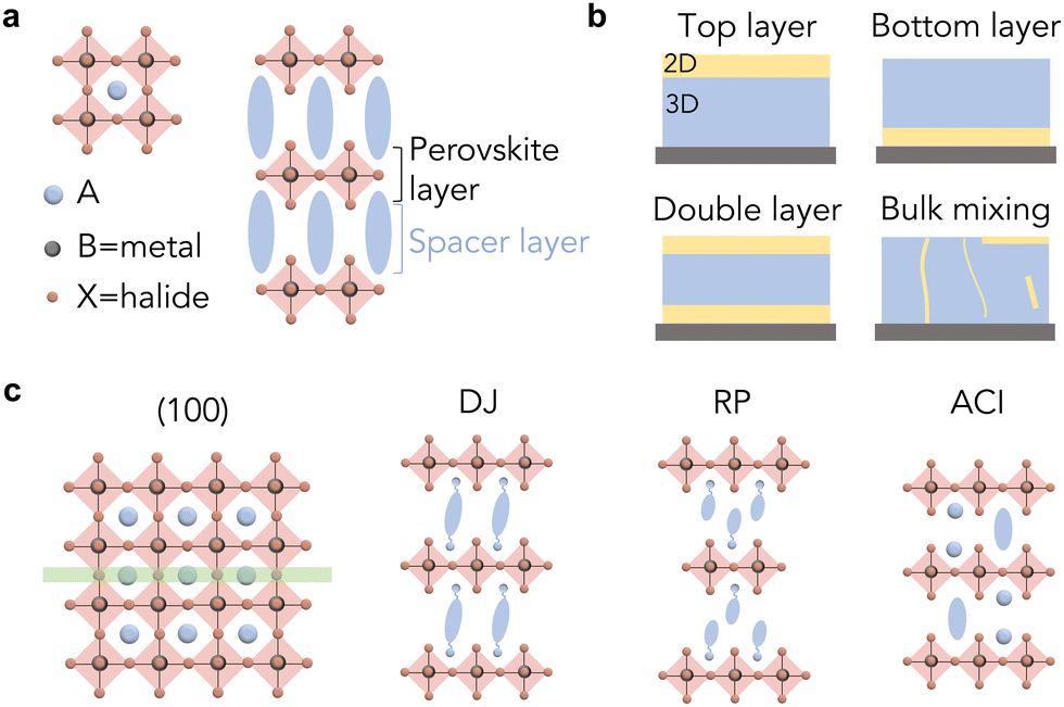 | ||
| Fig. 1 (a) Crystal structure scheme of 3D perovskite and 2D perovskite. (b) Scheme of heterostructure types of 2D/3D perovskite thin films. (c) Scheme of different space groups and phases of 2D perovskites based on (100)-orientation. | ||
Unlike pure 2D perovskites, 2D/3D heterostructures combine the stability of 2D perovskites and the carrier dynamics advantages of 3D perovskites, emerging as a leading structure in optoelectronic devices. Layered heterojunctions and bulk mixing are two major types of heterostructure (Fig. 1(b)), within which the layered heterojunction has been widely explored due to its ordered structure, controlled fabrication process and excellent device performance.18 The principle concept is to form 2D layers either on the surface or at the bottom of 3D perovskite grains (Fig. 1(b)), passivating the defects and also protecting the surface from the external environment. The most commonly used method for constructing 2D/3D heterostructures in devices is by depositing ligand salt solution onto as-synthesized 3D perovskite thin films and converting the surface of 3D perovskite into 2D perovskite in situ. This type of cation exchange and structural conversion mechanism has also been demonstrated in perovskite nanocrystals.19 Based on this method, different strategies, including solvent engineering,20–24 annealing engineering,25,26 and processing engineering27–29 have been developed to precisely manipulate the microstructures. Among them, for any given 2D perovskites, the ligand configuration is one of the most critical parameters that determines the structures and subsequently the optoelectronic properties and long-term stability of the desired materials.
In this feature article, we underline the performance-limiting characteristics in 2D/3D perovskite heterojunctions and leverage the key roles of organic ligands in determining these characteristics. By examining recent progress in understanding the structure and photophysical properties of 2D/3D heterojunctions, we build the structure–property-performance relationship to connect different aspects of previous research work on perovskite heterojunctions and to generate design principles for organic cation ligands. Meanwhile, we provide insights into the findings about the stability of 2D/3D heterojunctions in devices and effect of ligand configurations on structural stability. Finally, we also present perspectives on emerging directions to address critical issues that have not been solved for 2D/3D heterojunctions, specifically focusing on ligand design.
2. Structural characteristics of 2D/3D heterojunction
The structural characteristics of 2D/3D perovskite heterojunctions can be grouped into two types: the structure of 2D perovskites and the structure of 2D/3D heterojunctions. The description of the crystal structure of 2D perovskites encompasses the phase space, thickness of the inorganic layers (or so-called perovskite layers), and packing order of inorganic octahedra and organic cations, while that of the 2D/3D heterostructure includes relative orientation and morphology. In this review article, the general chemical formula of a 2D perovskite is written as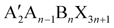 , in which A′ is the bulky organic ligand, and the n value is defined as the number of octahedral layers that are sandwiched by the organic spacers along the stacking direction. We list the most widely studied ligands for the construction of 2D/3D heterojunctions in Fig. 2 and will discuss the role of the molecular configurations of organic spacers in modulating the above-described structure characteristics.
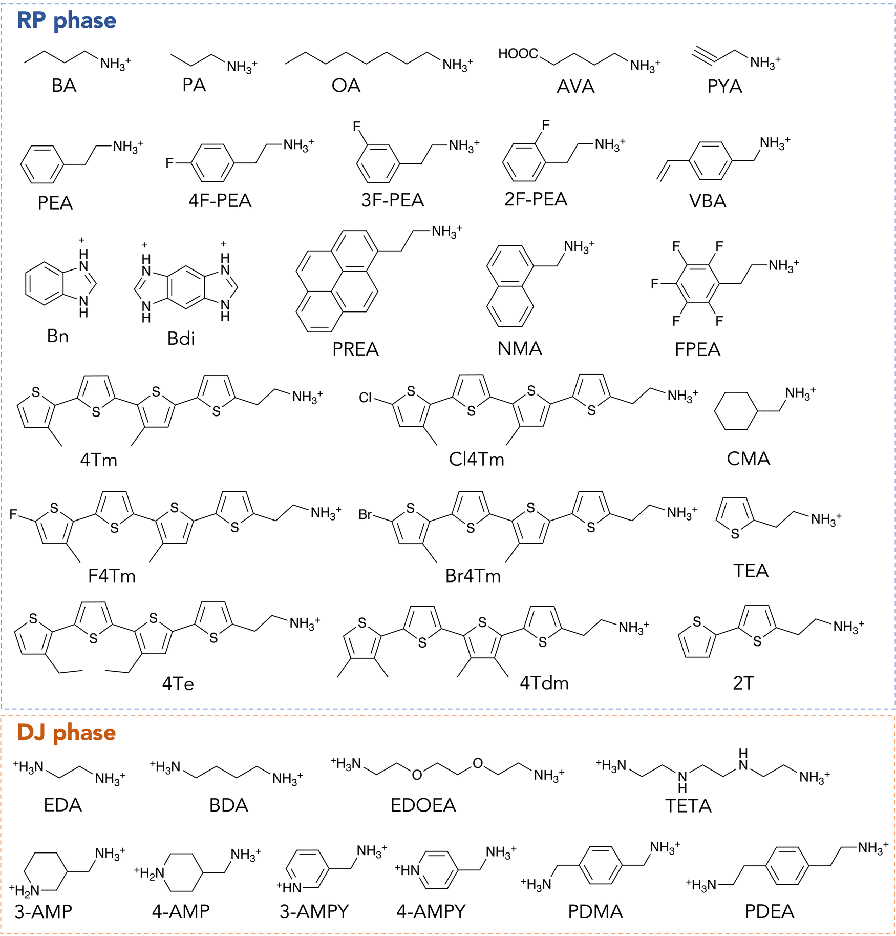 | ||
| Fig. 2 Molecular structures of representative examples of organic cations used for 2D/3D heterojunction construction. | ||
2.1 Phase spaces
The phase spaces of 2D perovskites can be classified into three types: Ruddlesden–Popper (RP) phase, Dion Jacobson (DJ) phase, and alternating cation (ACI) phase (Fig. 1(c)). The RP phase features a shift in the stacked perovskite layers by half a unit cell in the in-plane direction, while it can be considered as being formed with mono-ammonium functional ligands (Fig. 2). In contrast, the DJ phase is formed with diammonium ligands (Fig. 2) and exhibits no in-plane shift between the stacked perovskite layers.30 As described, the phase space of the formed 2D perovskite is closely related to the number of ammonium functional groups on the spacer ligands. The mono-ammonium ligands in the RP phase usually end with a neutrally charged tail, which interacts with ligands in the neighboring layer through intermolecular forces. Van de Waals force or π interactions stem from aliphatic tails or aromatic tails, respectively, and the representative ligands are butylammonium (BA) or phenethylammonium (PEA). In contrast, the DJ-phase 2D perovskite is composed of diammonium ligands, and the interactions between neighboring organic layers are considered to be covalent bonds. Notable differences in the out-of-plane and in-plane mechanical properties and structural stabilities between RP phase and DJ phase have been observed, attributed to the different interlayer interactions and stacking orders.The rigidity of the ligands and the bonding types between the neighboring organic layers are two key factors that influence the structure and mechanical stability of 2D perovskites. The intra-molecular covalent bonds in DJ-phase 2D perovskites are expected to be stronger than the intermolecular interactions in RP-phase 2D structures. The flexible BA ligand in the RP phase has been demonstrated to result in less distortion of octahedra in the in-plane direction, while the rigid 4-(aminomethyl)piperidinium (4AMP) ligand in the DJ phase gives rise to greater distortion due to the stronger electrostatic interactions between the cyclic diammonium cation and the inorganic octahedra (Fig. 3(a) and (b)).31 It has also been reported that with similar rigidity, the benzimidazolium (Bn) cations, which form an RP-phase 2D perovskite, have only weak intermolecular interactions to hold the structure together, while the divalent benzodiimidazolium (Bdi) cations shift the weakest link in 2D perovskite from intermolecular interactions to the bonds between cations and perovskite octahedra.32 RP- and DJ-phase 2D perovskites also exhibit significant differences in mechanical properties, including Young's modulus.33 Due to the thinner organic layer and greater proportion of space in the rigid inorganic layer, DJ-phase 2D perovskite exhibits increased moduli and subsequently enhanced mechanical stability, compared with an RP-phase structure.
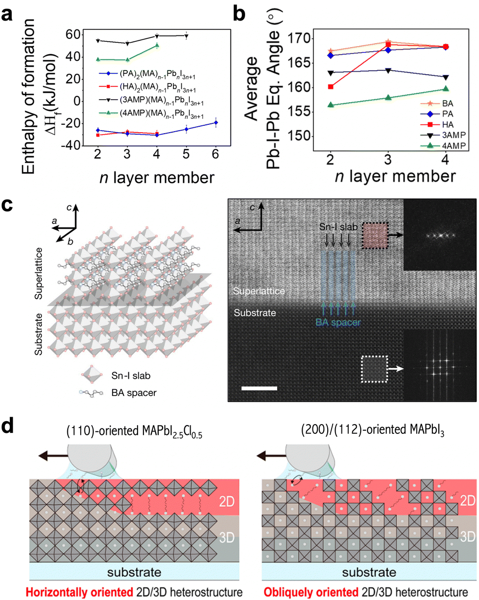 | ||
| Fig. 3 (a) and (b) Enthalpy of formation (a) and average equatorial Pb–I–Pb angle (b) for four different 2D perovskites as a function of perovskite layer thickness.31 Reproduced with permission.31 Copyright 2021, American Chemical Society. (c) Scheme (left) and atomic-resolution cryogenic STEM images (right) of (BA)2SnI4 vertically aligned on MAPb0.5Sn0.5Br3 single-crystal substrate.34 Reproduced with permission.34 Copyright 2022, Springer Nature. (d) Schematic illustration of heterostructures fabricated on (110)-oriented MAPbI2.5Cl0.5 or (200)-/(112)-oriented MAPbI3.47 Reproduced with permission.47 Copyright 2022, American Chemical Society. | ||
With regard to environmental stability, 3D perovskites with 2D capping layers are usually considered to show reduced moisture and oxygen penetration. In the case of RP-phase 2D perovskites, the expected ending layer on the surface consists of the tails of organic cations, which are neutrally charged and chemically stable. However, the surface ending group in DJ-phase perovskite will be either the unbonded ammonium functional group or the perovskite octahedral layer, neither of which is inert. The structure of DJ-phase 2D perovskite can be disrupted in a humid environment due to hydration, but the good news is that the original layered structure can be restored through annealing.36 This analysis indicates that the environmental stability of 2D/3D heterostructures with DJ-phase 2D perovskites is still debatable. Therefore, although RP-phase and DJ-phase structures have been used to create 2D/3D heterojunctions and been demonstrated with representative devices, there is no conclusion about whether one type of structure has dominant advantages over the other, given various aspects of the two phases.
2.2 Thickness of inorganic perovskite layer
Another type of phase group in 2D perovskite is defined by the thickness of its perovskite layers. In this manuscript, we use the term “n phase” to refer to this type of phase group. The structure and physical properties of n = 1 2D perovskites have seen intensive studies. However, limited understanding has been gained in thermodynamically stable 2D perovskite structures with n > 1, also called quasi-2D perovskites, mainly due to the challenges of synthesizing phase-pure (narrow n-value distribution) quasi-2D perovskite crystals.35,37 Therefore, the most studied growth methods of 2D/3D heterojunctions inevitably form a mixed-phase quasi-2D perovskite layer on top of 3D perovskite thin films. Various state-of-the-art strategies have been developed to control the phase distribution of quasi-2D perovskites in 2D structures and 2D/3D heterostructures, such as solid-state growth,27 control over annealing temperature,25 and solvent engineering,24 beside which the molecular configurations of organic ligands are the deterministic characteristics of a thermodynamically stable 2D structure (Fig. 3(a)).Chen et al. have demonstrated that the configuration of organic spacers can influence the phase purity and the preferred n values of the quasi-2D perovskite in a 2D/3D heterojunction.23 As bonding different ligands onto the quasi-2D perovskite flakes (FAn−1PbnI3n−1) will introduce different types of strain into the flakes due to the ligand packing geometry, the perovskite lattice has to be distorted to release the strain. Mostly, bulkier organic ligands result in more lattice strain, and thicker perovskite flakes are required to fully release the strain; thus, a larger n value is preferred. The intermolecular interactions between neighboring organic ligands, like hydrogen bonds, could also cause distortion of the octahedra in the inorganic layers, which subsequently modulate the n values.38–40 The same principle also applies to a DJ-phase 2D/3D heterojunction formed with 2,2-(ethylenedioxy)bis(ethylammonium) (EDOEA), in which suitable binding energy and hydrogen bonds between organic ligands and perovskite octahedra lead to the formation of a phase-pure n = 1 structure, instead of mixed phases.41 Beside determining the n phases through structural stability, the hydrogen bonding between cations like dimethyl adipimidate can induce uniformly distributed colloidal sizes in precursor solution and result in spontaneously formed phase-pure 2D perovskite at the bottom of 3D perovskite thin films.42 The other factor that influences the n values in 2D/3D heterojunctions is the lattice matching between 2D and 3D structures.43 A large lattice mismatch caused by the differences in halides and cations in 2D and 3D perovskites results in lattice strain at the interfaces, which facilitates the maintenance of the pre-crystallized n = 1 2D crystal in its original phase when incorporated into the 3D perovskite matrix, as phase transformation is less favorable. Based on this principle, the design of organic ligands can also play the role of generating large lattice mismatch between 2D and 3D perovskites, to stabilize the n phases. For example, the conjugated ligands offer various types of tunability on the molecular configurations to tune the lattice structures, such as heteroatom, conjugation length, and molecular twist (planarity), significantly suppressing the halide segregation and n-phase separation, which requires more investigation and applications on 2D/3D heterojunctions.44–46
2.3 Orientation of 2D perovskites
Due to its anisotropic structure and electronic properties, the orientation of a 2D perovskite in a device is critical in determining the carrier dynamics. The orientation of 2D perovskites in heterojunctions can be grouped into three categories: vertically aligned, parallel aligned, and randomly oriented, with respect to the bottom 3D perovskite substrates. Most 2D passivation layers in state-of-the-art PSCs are parallel aligned with 3D perovskites, as reported by the X-ray diffraction (XRD) and grazing incidence wide angle X-ray scattering (GIWAXS) patterns, due to the shallow ligand diffusion depth and the easy formation of parallel 2D perovskites on commonly used substrates.24,25 However, by slowing down the crystal growth rate, Lei et al. demonstrated the heteroepitaxial growth of a BA2MAn−1SnnI3n+1 2D crystal on an MAPb0.5Sn0.5Br3 3D perovskite single crystal, which exhibited a vertically oriented 2D structure (Fig. 3(c)).34 In addition to the relative lattice matching between vertically aligned BA2MAn−1SnnI3n+1 and the (100) facet of MAPb0.5Sn0.5Br3, it was shown that there is a stronger ionic bond between metal–halide and inorganic slabs in a vertically aligned structure, in comparison with the weak van der Waals force in parallel aligned structures, which also enables a thermodynamically stable and favorable orientation. These results demonstrated the tunability of the 2D perovskite orientation through lattice matching design and growth kinetic control. Lei et al. further reported that the 2D crystals grown on the (110) facet of a 3D perovskite form a rugged surface due to the change in orientation. This type of facet-dependent growth has also been reported in parallel aligned 2D/3D heterojunctions. The growth of 2D crystals based on the (200) or (112) facets of 3D perovskites exhibited a templated growth mechanism in which the orientations of the 2D perovskite match the 3D facets (Fig. 3(d)).47,48 The feasibility of tuning the orientation of a 2D perovskite through a 3D perovskite template proved its dissimilarity with pure 2D growth, with the interactions between ligands and the 3D perovskite lattice becoming a determining factor. Small modifications to the molecular configurations, such as fluorine-substitution, can alter the orientation of 2D crystals to either parallel or randomly oriented.49,50 The mechanism behind the change in orientation remains unclear, and may be further inspected to show a clear correlation between molecular configuration and crystal orientation.Another type of orientation refers to the relative in-plane orientation between 2D and 3D stacks. This type of orientation is discussed only when the 2D and 3D structures are parallel aligned in the out-of-plane direction. The ligands on the 2D perovskite surface interact with the surface of the 3D perovskite, which is coated with ligands that match those on the 2D perovskite, constructing an ordered interface due to lattice matching and the molecular interactions of the matched ligands.51 In other cases when the ligands on interfaces are not matching, the interface structure will be disordered with randomly twisted angles. An ordered interface is essential for surface passivation and favorable optoelectronic properties; however, it was not confirmed in most device-related reports. Given the polycrystalline nature and complicated surface environment of 3D perovskite thin films, the interface orientation requires further characterization to deepen the understanding of the microstructures. Although device-related 2D/3D heterojunctions contain matched ligands in most studies, the fast crystallization and formation process in device fabrication could result in a kinetic product, which may be disordered. In addition, with the development of 2D/3D heterojunctions, new types of heterostructure are emerging, like low-dimensional 2D perovskites with different metal cations,22 which present the possibility of incorporating unmatched ligands on 2D and 3D surfaces in the future.
2.4 Morphological characteristics of 2D/3D heterojunctions
Another scenario at the 2D/3D heterojunction is interface contact. Achieving a conformal coating of 2D perovskite on top of 3D perovskite usually requires the 2D layer to be sufficiently thin; otherwise, the stable 2D crystals will grow into large unoriented flakes, resulting in poor contact with the 3D perovskite surface.52 This issue can be addressed by modulating the ligand configurations and adjusting the 2D perovskite lattice strains.53 The increased bulkiness of the organic ligands leads to more lattice distortion and tilting of the octahedra, subsequently increasing the lattice strain, which inhibits the growth of large flakes, instead promoting the conformal coating of 2D crystals on the multigrain 3D perovskite surface. Furthermore, the bulkiness and solubility of the organic ligands can vary the relative location of 2D perovskite with respect to 3D perovskite thin film, such as spontaneously creating 2D perovskite at the bottom of 3D perovskite thin films.54 Thus, engineering the ligand configuration may be used in controlling the crystallization process, in a mixed precursor solution and during the surface reconstruction process.3. Photophysical characteristics of 2D/3D heterojunctions
The photophysical properties in 2D/3D heterojunctions are essential for their applications in photovoltaics and other optoelectronic devices. Due to the vitally important role of carrier dynamics in determining the performance of a device, it has attracted tremendous attention. As discussed in an earlier section, the molecular configuration of spacer ligands can be tuned to manipulate the structural characteristics of 2D/3D heterojunctions. It also influences defect passivation, energy level alignment and further the carrier dynamics in 2D perovskite and 2D/3D heterojunctions. Understanding the influential factors of carrier dynamics at heterointerfaces is equally as important as developing strategies to tune structures and gain control over their properties.3.1. Trap state passivation
Non-radiative recombination, caused by the trap states, is a major factor that results in charge transfer loss at a heterointerface. One major goal of designing a 2D/3D heterojunction is to reduce the defect-induced interface recombination between 3D perovskite and the charge transporting layer. Among various molecular passivators, an ammonium-functionalized organic cation is a typical type of passivator to coordinate with negatively charged defects.8,55 Time-resolved microwave conductivity has been used to probe the carrier lifetime and the defect-induced recombination rate at a 2D/3D heterojunction formed with a BABr ligand.56 2D/3D heterostructures exhibit a prolonged carrier lifetime, suggesting a reduced recombination loss in comparison with a 3D perovskite. However, there is also a report claiming that a 2D/3D heterostructure can result in increased electronic disorder in certain situations, causing an exponential decrease in charge-carrier mobility.57 The extrinsic deep trap states generated during the formation of a 2D perovskite can exacerbate non-radiative charge recombination, which becomes a trade-off effect of a 2D perovskite.58 Nevertheless, reducing the surface defects and eliminating non-radiation recombination at the surface is a widely accepted role of a 2D/3D heterojunction. However, the differences in passivation mechanism between heterojunctions and pure ammonium-functionalized organic cations are still unclear. A recent study exhibited a new concept in which the band structure of a 2D/3D heterojunction is mainly responsible for the ultralow interfacial recombination.59 The formation of a 2D/3D heterojunction results in band bending at the surface of a 3D perovskite, which repels the charge carriers from the defective surface, thereby reducing the interfacial recombination rate. This result indicates that the reduced defect densities on the 3D perovskite surface may not be the dominant reason for the reduced recombination rate, while the energy band structures can have a more significant impact on carrier dynamics.27 The optimized energy level offset between 2D and 3D perovskites has also been calculated to increase the tolerance of interfacial defects, further demonstrating the importance of energy levels at the heterojunctions.603.2. Energy level alignment
Since a 2D perovskite is formed with alternating organic and inorganic layers, which defines its low dimensionality, the quantum confinement effect influences its electronic structure and enlarges the bandgap of this type of material.30 Thus, a 2D/3D heterojunction is usually formed between wide-bandgap and narrow-bandgap semiconductors. Either type-II54,61,62 or type-I22,29,63,64 energy alignment could be formed at this heterojunction. There is still no consensus on the type of energy alignment formed at 2D/3D heterojunctions. Type-I alignment indicates that the 2D perovskite can reduce surface non-radiative recombination, while type-II alignment facilitates charge transfer and the spatial separation of electrons and holes, which is desirable for most device structures.The n value can determine the bandgap of 2D perovskite, but more importantly it influences the relative energy levels between 3D and 2D perovskites. Increasing the n value will shrink the bandgap of 2D perovskite, as well as changing type-I alignment to type-II alignment in certain scenarios (Fig. 4(a)).24 The typical method of constructing a 2D/3D heterojunction is by spin coating the ligand solution onto 3D perovskite thin films and converting the surface of 3D perovskite into a 2D structure through cation exchange. The mixed phases resulting from this type of construction method make it challenging to control the energy landscapes. Efforts have been devoted to achieving type-II alignment at the 2D/3D heterojunction through controlling the phases of 2D perovskite based on device engineering and ligand configurations.23,24 Since conventional and inverted device architectures require hole extraction or electron extraction at the top surface, respectively, different type-II alignments are required. While hole extraction through proper energy alignment of a 2D/3D heterojunction has been widely studied and used in devices with a conventional architecture, new strategies for constructing 2D perovskites to facilitate electron extraction have just emerged. Usually, increasing the n value of the 2D perovskite will have a more significant effect on the conduction band energy level, which is critical for electron extraction.23,25
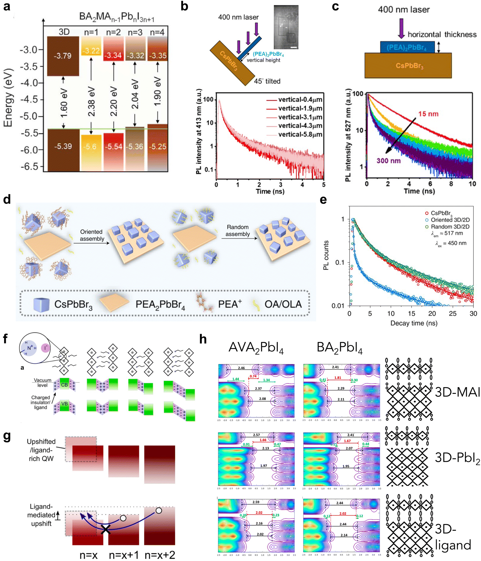 | ||
| Fig. 4 (a) Energy level alignment of 3D and BA-based 2D perovskites with different n values.24 Reproduced with permission.24 Copyright 2022, The American Association for the Advancement of Science. (b) Scheme of vertically aligned (PEA)2PbBr4 on CsPbBr3 heterostructure (top) and TRPL of the 2D emission in these heterostructures collected at different vertical heights (bottom). (c) Scheme of a horizontally aligned 2D/3D heterostructure (top) and TRPL spectra of the emission from CsPbBr3 with varying thicknesses of 2D perovskite (bottom).65 Reproduced with permission.65 Copyright 2021, American Chemistry Society. (d) Scheme of CsPbBr3/(PEA)2PbBr4 heterostructures via oriented or random assembly. (e) TRPL spectra of the emission from CsPbBr3 in heterostructures.51 Reproduced with permission.51 Copyright 2022, Springer Nature. (f) Scheme of the dipole moments in 2D perovskite ligands misaligned with the energy levels of the neighboring 2D phase. (g) Type-II interfaces resulting from ligand-induced band upshifts.66 Reproduced with permission.66 Copyright 2019, American Chemistry Society. (h) Density of states and band alignments of 2D/3D heterostructures with different 3D perovskite surface terminations and 2D perovskite ligands.67 Reproduced with permission.67 Copyright 2020, American Chemistry Society. | ||
The charge carrier dynamics also vary according to the orientation of the 2D perovskite in the heterojunction, due to anisotropic properties.30,68 3D CsPbBr3 single-crystal thin film and solution-grown (PEA)2PbBr4 have been used to demonstrate the orientation effect of the 2D perovskite in a heterojunction.65 Vertically aligned 2D perovskite flakes on CsPbBr3 promote efficient charge transfer (Fig. 4(b)), while horizontally aligned 2D flakes modulate the energy alignment based on the layer thickness (Fig. 4(c)), as confirmed by time-resolved photoluminescence (TRPL). Thin 2D flakes exhibit type-I alignment, but thicker 2D flakes (>150 nm) are more likely to behave with type-II alignment, facilitating more efficient charge transfer. Since the orientation of 2D perovskites changes the defect density and charge transport efficiency, omission in considering these features could cause discrepancies in the actual roles of heterojunctions.
As the orientation of the heterojunction also includes the in-plane orientation and lattice matching between 3D and 2D perovskites, Zhu and co-workers unveiled the mechanism of carrier dynamics influenced by these factors.51 They developed an epitaxial welding method to control the in-plane orientation (Fig. 4(d)) and demonstrated that the ordered interfaces with matched lattice parameters reduce the lattice strain and improve the charge carrier transfer at the interfaces (Fig. 4(e)). Owing to the limitations of the current 2D/3D model, this type of disordered heterojunction has not been considered in device applications, but needs to be investigated urgently to approach the theoretical limit of device performance.69
As enormous empirical efforts have been invested in controlling energy alignment at a heterojunction, there is a lack of a principle that can guide the design of a heterojunction to achieve proper energy alignment, as the scenarios differ case-by-case. This is due to various heterojunction composition and the lack of advanced techniques to probe the accurate energy levels at the interfaces precisely but can also be caused by the complicated chemical environment on the surface. For example, without a perfect interface between 2D and 3D perovskites, the ligand density between them can vary. As the surface charge density is known to shift the effective work function of the material, the various amounts of ligand cations consequently change the energy alignments at a 2D/3D heterojunction (Fig. 4(f) and (g)).66 Although calculation showed that ligand–ligand interaction is thermodynamically favored in comparison with the interactions between ligand and other 3D fragments terminated with MA or PbI2,52 it is challenging to avoid forming other types of interface during the rapid growth process of a 2D/3D heterojunction. Recently, Traoré has developed a computational methodology to inspect the energy alignment at a 2D/3D heterojunction with CsPbI3 and (PEA)2PbI4, considering all the different factors, including the termination and relaxation of the 3D perovskite surface, the passivation effect and dipole formation.70 It was demonstrated that the interplay between dipoles of different systems can lead to the readjustment of energy level alignment at interfaces, with respect to the energy levels obtained from each individual system. Calculation methods have also been developed to examine the energy level alignment between (BA)2PbI4 or (AVA)2PbI4 (AVA = protonated aminovaleric acid) 2D perovskite and MAPbI3, and they clearly showed that the surface termination of MAPbI3 and the confined dipole of the ligands play critical roles in determining the energy alignment.67 (BA)2PbI4 always forms a type-II alignment with MAPbI3 but with alternating band-edge position with regard to the termination of 3D perovskite, while (AVA)2PbI4-MAPbI3 interfaces could change from type-I to type-II alignment with respect to different terminations (Fig. 4(h)). Although there is still a lack of experimental verification, the surface-environment-induced dipole change in 3D perovskite thin films already gives rise to challenges in designing predictable energy alignment at the heterojunction.
Besides these static chemical structures, light illumination can alter the charge behavior at the heterojunction. It was reported that a 2D perovskite exhibited light-induced lattice contraction, due to the flexibility of the organic cations and hole accumulation under illumination, which overcame the charge transfer problems in 2D perovskites.71 A special heterostructure has also been designed to insert a 2D layer at the grain boundaries of 3D perovskite thin film, and the photogenerated charge carriers have been observed to fill the interfacial traps under illumination and subsequently increase the built-in potential at interfaces and block electron transfer.72 Conversely, the built-in potential facilitates hole extraction from 3D perovskite to 2D perovskite, which indicates that the structure can be effectively applied between the perovskite and the hole-transporting layer in solar cell devices to support hole extraction. Owing to these uncommon photoinduced phenomena, charge carrier dynamics characterized by different techniques under various conditions, such as light-activated spectra, should be considered carefully. There is also a report demonstrating strong Coulombic coupling between different perovskite n phases due to overlap of their wave functions, promoting an ultrafast carrier transfer rate of <100 fs.73 The unexpected ultrafast interfacial charge transfer and the compatibility of energy and charge transfer at these heterojunctions explained why they can be used to realize high-performance solar cell devices and LED devices at the same time.
3.3. Carrier dynamics in pure 2D perovskite
Another parameter that influences the charge transfer properties at a heterojunction is the carrier dynamics of the 2D perovskite itself, as efficient charge transfer in the 2D perovskite avoids charge accumulation and recombination at the interfaces. Out-of-plane charge transfer in a 2D perovskite can be considered to be a tunnelling process between inorganic layers, mediated by the organic interlayer. The tunnelling distance and height are equally important in determining the charge transfer properties. The distance can simply be tuned by the length of spacer ligands, or changes between the DJ phase and RP phase. For instance, DJ phases are expected to show excellent carrier transmission properties, due to their shortened interlayer distances, eclipsed stacking arrangement, and enhanced coupling between Pb–I inorganic layers.74–76 Therefore, DJ-phase 2D perovskites in 2D/3D heterojunctions also exhibited improved charge transfer ability.61 In contrast, the barrier height is more complicated. In general, two main characteristics could tune the barrier height: electronic coupling between neighboring ligands, and energy level alignment between the inorganic perovskite layer and the organic spacer layer. Functional groups on the spacer ligands, such as fluorination of PEA77,78 and other halide-modified ligands,38 alter the formation energy and change the stacking geometry of the organic spacers from face-to-edge to face-to-face through hydrogen bonding (Fig. 5(a)), consequently enhancing the interlayer electronic coupling (Fig. 5(b)). The energy level alignment is usually tuned by introducing conjugated molecules into the spacer ligands, to achieve matched energy levels between organic and inorganic layers.79 As initially designed and studied by Mitzi and recently extensively explored by Dou, organic-semiconductor-induced 2D perovskites can be constructed to form either type-I or type-II energy alignment between inorganic and organic layers with modified conjugated thiophene or selenophene ligands.38,80–83 The carrier dynamics depend vitally on the energy level alignment, exhibiting light emission from either the Pb–I layer or the organic layer, or quenching the emission due to charge separation (Fig. 5(c)). It has also been proved that an organic–semiconductor-incorporated 2D perovskite can lead to a long-lived charge-separated state over the nanosecond timescale due to type-II alignment.84 In addition, the conjugated ligands modify the hydrogen bonding and the supramolecular π-stacking between them, resulting in excellent out-of-plane conductivity from both aspects (Fig. 5(d)).38,85 Further modification of the conductivity and optoelectronic properties can be achieved by designing charge transfer complexes in the organic layer, such as combining the charge-donating and charge-accepting molecules.86,87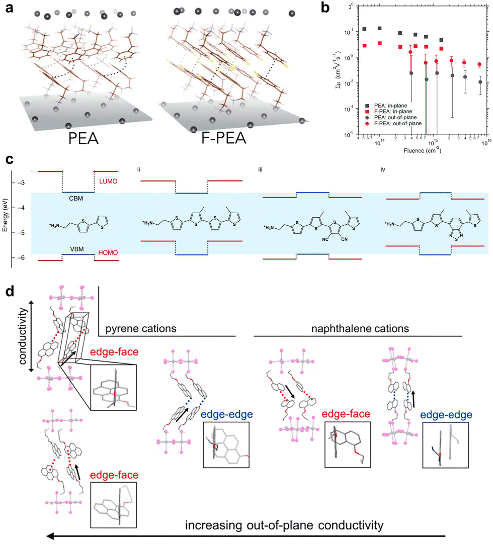 | ||
| Fig. 5 (a) Structures of (PEA)2PbI4 and (F-PEA)2PbI4 2D perovskite single crystals. (b) Time-resolved microwave conductivity of out-of-plane and in-plane carrier transport in 2D perovskite thin films with different ligands.77 Reproduced with permission.77 Copyright 2019, American Chemistry Society. (c) The energy level alignments of organic (red lines) and inorganic (blue lines) layers within 2D perovskites with different conjugated ligands.80 Reproduced with permission.80 Copyright 2019, Springer Nature. (d) The influence of ligand stacking in 2D perovskites on the out-of-plane conductivity.85 Reproduced with permission.85 Copyright 2018, American Chemistry Society. | ||
In-plane charge transfer occurs mainly within the inorganic perovskite layer, in which the organic spacers do not participate directly. However, the intermolecular interactions between the organic molecules, in-plane and out-of-plane, influence the tilting of octahedra in the inorganic lattice, thereby affecting the in-plane charge transfer properties. As reported by Yao et al., a significant increase in the in-plane carrier mobility of Sn-based 2D perovskite can be achieved by manipulating the molecular configuration of the conjugated ligands.81 The bandgaps and hole mobilities can also be tuned by equipping the spacer ligands with chemical moieties that can interact with the ammonium group on the adjacent ligand across the organic bilayer.40
4. Solar cell devices with 2D/3D heterojunctions
The construction of 2D/3D heterostructures has contributed to an increased number of high-efficiency devices, due to grain boundary passivation, energy landscape management, and stability enhancement. There are two ways to introduce 2D/3D heterostructures into PSCs. One method involves mixing the precursors of 2D perovskite and 3D perovskite together to spontaneously form a phase-segregated 2D/3D heterostructure in bulk perovskite.88 The other method is to deposit a 2D perovskite capping layer on top of a 3D perovskite thin film to adopt a planar 2D/3D heterostructure as a post-treatment. The latter method is usually adopted to avoid the formation of a quasi-2D perovskite and to limit the amount of 2D perovskite in the bulk material. But the specific treatment process still depends on the ligands and the formation energy of 2D perovskites. The molecular configuration of the ligand is of great importance in tuning the structural properties and optoelectronic properties of the heterostructures, and it plays a key role in determining the device performance. The following section is a diagram of several strategies for enhancing the device performance through the molecularly-tuned structure and photophysical characteristics of 2D/3D heterojunctions.4.1. DJ-phase 2D perovskite in a heterostructure
While the RP phase is the most commonly used structure for 2D/3D solar cell devices, the ACI phase has also been used occasionally.89 Compared with them, DJ-phase 2D perovskite materials, owing to their smaller interlayer distances and expected excellent charge transfer properties, represent another important type of 2D perovskite in 2D/3D heterostructures that can be applied to PSCs. Commonly used diammonium cations include aliphatic ethane-1,3-diammmonium (EDA), butane-1,3-diammmonium (BDA), octane-1,3-diammmonium (ODA), and aromatic 3-(aminomethyl)piperidinium (3-AMP).90–96 One of the best-performing DJ-phase 2D/3D PSCs features a metastable alternating head-to-tail capping layer, achieving a highest efficiency of up to 24.7% (Fig. 6(a)).61 The use of an asymmetric organic cation N,N-dimethyl-1,3-propane diammonium (DMePDA), which contains a primary ammonium terminus and a tertiary ammonium terminus with a less-stable packing geometry in a 2D structure, demonstrated weakened hydrogen-bonding interaction. This effect leads to an uplifted valence band maximum for the organic layer and decreases the band offset between the inorganic framework and the organic moieties, improving the hole transport from shortened charge tunnelling distance and decreased energy barriers.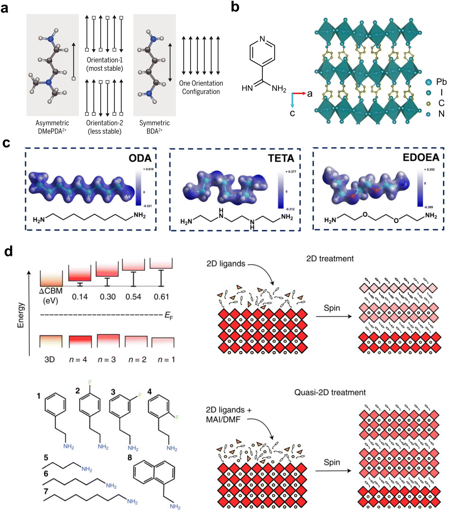 | ||
| Fig. 6 (a) Two possible arrangements of asymmetric DMePDA2+ cations and the only arrangement of symmetric BA2+ cations.61 Reproduced with permission.61 Copyright 2021, The American Association for the Advancement of Science. (b) The molecular structure of 4AP and the single-crystal structure of (4AP)PbI4.97 Reproduced with permission.97 Copyright 2023, Elsevier. (c) The molecular structures of ODA, TETA and EDOEA and their corresponding electron-density distributions.98 Reproduced with permission.98 Copyright 2021, John Wiley and Sons. (d) Band alignment of 3D and 2D perovskites with different n values and the ligands used in the study (left) and schemes of the 2D and quasi-2D treatment processes (right).23 Reproduced with permission.23 Copyright 2022, Springer Nature. | ||
Among the aromatic diammonium cations, which have more rigid structures and potential π-interactions between organic layers, pyridine-functionalized ligands and (phenylene)di(ethylammonium) (PDEA) are the most widely studied in 2D/3D heterojunctions. Adopting pyridine units, 3-aminomethylpyridine (3-AMPY) and 4-aminomethylpyridine (4-AMPY) were reported to form a DJ phase on top of 3D perovskite, with a smaller conduction band offset between the 2D and 3D perovskites compared with their RP-phase analogs.21 Assisted by solvent engineering, the reconstruction of the perovskite surface with 3-AMPY results in a uniform and large n value in DJ phases, favorable band alignment and an elongated electron diffusion length, which facilitate efficient electron tunnelling. With further development of FAPbI3-based PSCs, the lattice matching between the amino group on the organic ligand and the FAPbI3 lattice becomes critical. 4-Amidinopyridine (4AP) with a unique amidino terminus, which matches the crystal lattice based on FA+ cations, was first reported in a DJ-based 2D perovskite for the formation of 2D/3D heterostructures in PSCs (Fig. 6(b)).97 According to an in situ photoluminescence (PL) spectral study, (4AP)PbI4 assists the nucleation and helps decrease the voids and defect densities of the 3D perovskite. The highest PCE can reach 24.9% for conventional devices. Similarly, an in situ surface reaction was found by using 3-AMPY, which generates pyridine-based ligands with similar formamidinium termini after reacting with a surface FA cation.99 However, n-type doping from surface engineering plays a key role in the devices rather than forming 2D/3D heterostructures.
Introducing a heteroatom into the aliphatic chain of diammonium cations can change the intermolecular interactions and subsequently tune the inorganic lattice tilting angles and help to build high-performance PSCs. EDOEA (Fig. 6(c)) with an oxygen heteroatom was used to form phase-pure n = 1 DJ-phase microcrystals vertically aligned at the grain boundaries of 3D perovskites.41 The minimization of photogenerated charge carrier localization in the 2D perovskite by a phase-pure structure demonstrated a champion efficiency of 21.06% in MAPbI3-based solar cells. Later on, a more comprehensive study was performed, which explained the regulation of charge transfer properties through the tilting of inorganic octahedra when different heteroatoms, i.e. N in TETA and O in EDOEA, interact with the [PbI6]2− framework.98 A deeper understanding of binding energy and hydrogen bonds in different ligands revealed that EDOEA is the most suitable ligand for a high-quality perovskite, yielding a triple-cation-based device efficiency of up to 22.68%.
4.2 2D perovskite n-phase modulation in a heterojunction
The n value of a 2D perovskite is another significant characteristic that influences the performance of PSCs. It has been found that the n values can be tuned by a molecular engineering approach due to the differences in formation energy.23,50 In particular, a wider layer width is preferred when translating the 2D/3D heterostructure from conventional devices to inverted devices, because of the electron-blocking nature of a low-width n = 1 perovskite. BA was found to be able to form phase-pure n = 2 perovskite capping layers when directly spin coated on a 3D perovskite surface, but 3-fluoro-phenethylammonium (3F-PEA) can preferentially form mainly n = 3 2D layers with the addition of MAI, superior to BA- or PEA-based 2D or quasi-2D perovskites (Fig. 6(d)). The reduced energy barrier for electron extraction allowed a PCE of 23.91% for inverted PSCs. The formation energy calculation for high-n-value PEA- and F-PEA-based 2D perovskites in this study made a compensation in the earlier calculation on n = 1 2D perovskite,78 providing a full spectrum for the possibility of forming different types of 2D perovskite.4.3 2D orientation modulation in a heterojunction
Control over the orientation in 2D PSCs is one of the most critical factors that influences device efficiency, as the vertical alignment of 2D perovskite increases the charge transfer efficiency by orders of magnitude. However, the situation in a 2D/3D heterojunction differs from that in pure 2D devices. While the fluorination of PEA has been found to be able to tune the 2D perovskite orientation on top of a 3D perovskite, the device results demonstrated that a parallel oriented 2D perovskite, formed with PEA, exhibited a better defect passivation effect, while the randomly oriented F-PEA-2D perovskite showed a limited effect of passivation.49,50 However, a recent study claimed that an obliquely oriented DJ-phase 2D perovskite, template grown from the (110) facet of MAPbI2Br, exhibited enhanced solar cell performance compared with a parallel oriented 2D crystal due to its improved charge transfer property.48 It remains controversial whether a vertically aligned or parallel aligned 2D crystal is favourable for the device performance of 2D/3D solar cells, and a careful study is needed, taking all factors, including the n-phase purity, orientation and energy alignment, into consideration.4.4 Energy level alignment with conjugated ligands
Ligands with a single aromatic ring, like PEA,26 F-PEA,23,77 pentafluoro-phenylethylamine (FEA)100 or thiophene-ethylamine (TEA) cations,101 are firstly reported to passivate the surface defects and control the crystallization process. Their small-molecular nature allows them to form 2D/3D heterostructures easily, but the strategy of manipulating energy level alignment at the interface is limited. Using conjugated cations as ligands allows tuning of the energy level alignment in 2D perovskite quantum wells, as well as in 2D/3D heterojunctions. However, increasing the conjugation also increases the size of the organic components, making it crucial to strike a balance between conjugation and the ability to form a 2D perovskite. From the molecular design perspective, increasing the number of phenyl or thiophene units can narrow the bandgap and shift the valence band maximum (VBM) of 2D perovskites.79,102 Ma et al. designed a multifunctional capping layer (MCL) with a quarter-thiophene backbone (4Tm) in conventional solar cells (Fig. 7(a) and (b)).103 This 2D/3D interface modifier upshifted the VBM and efficiently improved hole extraction from the perovskite layers and also retarded interfacial non-radiative decay via charge recombination. As a result, the device efficiency improved from 19.94% to 22.06%. Similarly, by increasing the phenyl conjugation, a two-ring naphthalene-based ligand, 1-naphthylmethylammonium bromide (NMABr), was used to construct type-II alignment at the 2D/3D interface and the highest efficiency reached 21.09%.104 Further enlarging the phenyl conjugation, Xue et al. recently reported pyrene-based A-site cations for tuning the electronic state at the band edge (Fig. 7(c)),105 although the crystal structure of pyrene-based 2D perovskites was not new and dates back to as early as the 1900s.106 Through the tuning of alkyl chain length, the molecular intercalation distance of pyrene can be adjusted to optimize electronic coupling, in which an ethyl chain demonstrated the best performance with a PCE of 23.0%.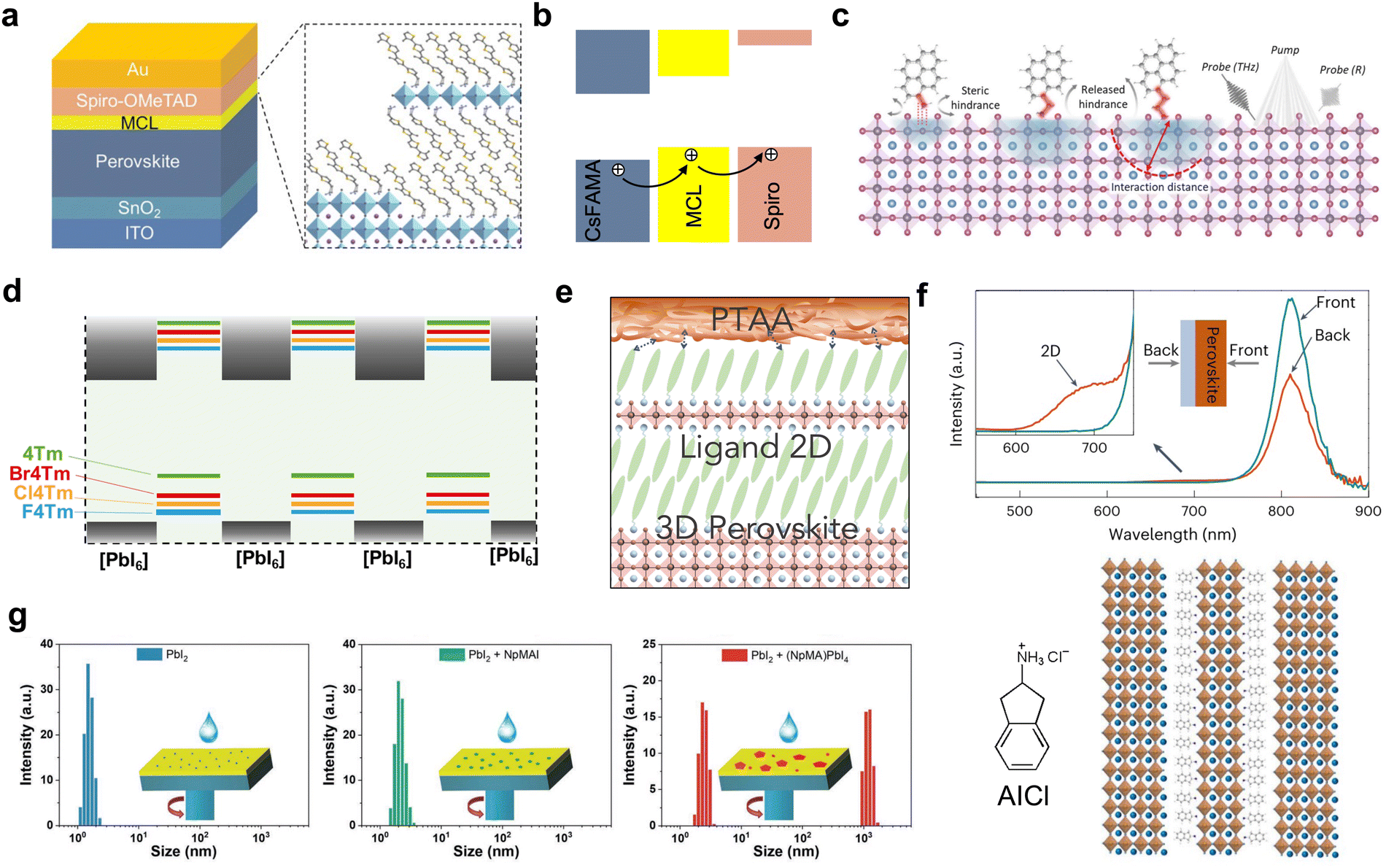 | ||
| Fig. 7 (a) Structure of a perovskite solar cell device based on the MCL-modified interface and schematic illustration of the MCL structure. (b) Energy level alignment and charge transfer direction.103 Reproduced with permission.103 Copyright 2021, John Wiley and Sons. (c) Scheme of the influence of ligand alkyl chain length on the interaction distance. Reproduced with permission.105 Copyright 2022, The American Association for the Advancement of Science. (d) Energy level alignments between inorganic and organic layers within a 2D perovskite formed with conjugated ligands.38 (e) Scheme of 2D perovskite structure between PTAA and 3D perovskite.53 (f) PL spectra of the 2D/3D perovskite thin films obtained from different incident directions (top) and the scheme of 2D structures formed with AICl (bottom).54 Reproduced with permission.54 Copyright 2023, Springer Nature. (g) Aggregation size distribution in precursor solutions of PbI2 mixed with either NpMA or (NpMA)2PbI4.107 Reproduced with permission.107 Copyright 2022, John Wiley and Sons. | ||
Beside increasing the number of conjugated rings, electron-withdrawing halogen substitution has been proven to be another efficient approach to achieve the delicate band offset adjustment of a 2D/3D heterostructure (Fig. 7(d)).38 Fluoro-, chloro-, and bromo-4Tm were designed and synthesized based on 4Tm through halogenation reactions using N-fluorobenzenesulfonimide, N-chlorosuccinimide and N-bromosuccinimide reagents, respectively. For Cl4Tm, the smallest energy level offset was observed at the 2D/3D heterojunctions, and the as-formed solar cells demonstrated optimized performance with PCEs up to 24.6%. Another critical factor contributing to performance enhancement is improved out-of-plane conductivity, resulting from interlayer halogen interaction, evident from conductive atomic force microscopy (cAFM) and microwave-conductivity characterization.
While the 2D/3D heterostructure is widely adopted in fabricating PSCs for electronic state management, the surface homogeneity of the 2D capping layer is often overlooked, despite its crucial role in inhibiting ion migration and enhancing environmental stability. By adjusting the side-chain of the quarter-thiophene backbone, it was observed that changes occurred not only in the physical solubility of ligand molecules but also in the growth dynamics and morphology of 2D/3D heterostructures.53 For the 4Te ligand, which replaces the methyl groups on 4Tm with ethyl groups, the solubilizing ethyl side-chain and the bulkiness increase the lattice strain in the 2D perovskite, leading to the formation of a more uniform 2D perovskite coating rather than segregated islands of 2D crystals. Further, due to the conformal 2D layers in the 2D/3D heterostructure, the binding between the polymer hole-transporting layer poly(triaryl amine) (PTAA) and bulk 3D perovskite is strengthened, as evident from a mechanical peeling test (Fig. 7(e)). Up to now, the exploration of large, conjugated cations used in 2D/3D heterostructures is still limited, and there is a lack of guidelines for new ligand design. More exotic structures and detailed analyses that lead to the development of new materials are still needed in this field.
4.5 Perovskite thin film structural modulation
The molecular configuration and its corresponding 2D/3D heterostructure can further influence devices with respect to the properties of the bulk perovskite materials and the bottom interfaces. For bulk perovskite optimization, anions in ammonium salts can not only serve as additives for adjustment of the surface work function, such as octylammonium tosylate on 3D perovskite but also tune the crystallization and dimensionality of low-dimensional perovskite, as seen in neo-pentylammonium (neoPA) chloride, bromide and iodide.108,109 In addition, acids such as β-guanidinopropionic acid (β-GUA) and 4-guanidinobutanoic acid (GBA) can function as crystallization control additives when incorporated into bulk perovskites and form 2D/3D heterostructures at the same time.110,111 Buried interfaces can be improved by forming 2D crystal seeds at the bottom, which regulate the growth of 3D perovskite. Li et al. reported the employment of 2-aminoindan hydrochloride (AICl) at the buried interface (Fig. 7(f)).54 Because of the poor solubility of AICl, the pre-existing nucleates in 3D perovskite precursors manipulated the crystallization process and improved the film quality. Similarly, in the sequential deposition method of 3D perovskite, 1-naphthalenemethylammonium (NpMA) with the form of a 2D structure can be introduced into the PbI2 precursor layer, followed by cation deposition, which enlarges the grain size of 3D perovskite crystals (Fig. 7(g)).107 Overall, it encourages the pursuit of a series of molecular designs, to draw more comprehensive conclusions and in-depth understanding through systematic studies. This approach should not be limited to a specific device configuration or one “super” molecule.5. Light-emitting diode device with 2D/3D heterojunctions
2D and quasi-2D perovskites have been widely used in fabricating light-emitting devices, due to their quantum confinement properties, high photoluminescence quantum yields, and tunable emission spectra. However, with further development, the need for light emission from the 3D perovskite layer initiated the need for designing efficient and stable 3D perovskite LEDs. Therefore, the perovskite 2D/3D heterojunction structure has emerged.The role of the 2D/3D heterojunctions in current LED devices focuses mainly on the defect passivation of 3D perovskite surfaces.112–115 Phenylalkylammonium iodide was first reported for application on 3D perovskite LEDs to reduce surface defect density and suppress iodide ion migration through the steric and Coulomb interactions of the passivating molecules.115 Although no 2D structures were observed, the report did not deny the possibility of forming ultrathin 2D perovskites. Other reports clearly showed the formation of 2D perovskites on top of 3D crystals with phenyl-based ammonium salt.112,113 It was reported that through a proton transfer method to introduce benzylamine onto the 3D perovskite surface (Fig. 8(a)), the 2D perovskite crystallized without destroying the bottom 3D structures and effectively suppressed the formation of trap states and ion migration, enhancing efficiency (Fig. 8(b) and (c)).112 Besides tuning the 3D perovskite emission wavelength through composition change,116 the quantum confinement strategy can also be applied to the 3D perovskite thin film by introducing PEA-based 2D perovskites, which passivated the 3D perovskite surface and simultaneously shrank the grain size and lowered the emission wavelength.113,117 A record champion external quantum efficiency (EQE) of 12.3% at 478 nm with 3D perovskite was achieved.
 | ||
| Fig. 8 (a) Scheme of surface treatment of 3D perovskites with benzylamine through proton transfer, or with aniline. (b) Scheme of the charge carrier dynamics in pure 3D and 2D/3D hybrid structures. (c) External quantum efficiency (EQE) of the pure 3D and 2D/3D hybrid LED devices.112 (d) Scheme of the crystallization pathway of epitaxially grown 2D/3D heterojunction (left) and the energy level alignment (right).114 Reproduced with permission.114 Copyright 2024, Springer Nature. | ||
In addition to trap state passivation, the energy level alignment of the 2D/3D perovskite structure is a critical factor for the efficient radiative recombination of electrons and holes within emission materials. Unlike solar cell devices, a gradient n phase in an LED device can generate energy cascade channels to induce charge transfer from the 2D to the 3D phase and increase the densities of injected electrons and holes. It was reported that the mixture of PEABr and guanidinium bromide (GABr) as organic ligands can generate cascade channels while improving the defect passivation effect.118 With proper energy alignment between 2D and 3D perovskites, the hole-transporting layer in the device can even be replaced by a 2D perovskite layer.114 Min et al. have developed a method to directly spin coat epitaxially grown 2D/3D heterojunction in Sn-based LED devices, creating an interface with matched out-of-plane and in-plane lattice alignment, minimizing the interface defect density and performing efficient hole transfer (Fig. 8(d)). As a result, this hole-transporting-layer-free device exhibited an EQE of 11.6% for near-infrared emission.
Currently, the study of 2D/3D heterojunctions in LED devices is underdeveloped, while most studies still focus on conventional ligands such as PEA113,114,116,117 and BA,119,120 with occasional exploration of other benzamidine and NMA ligands.121,122 We expect that more of the ligand types that are used in the construction of 2D perovskite LEDs will be adopted in 2D/3D heterojunction systems.
6. Photodetector with 2D/3D heterojunctions
The application of a perovskite in photodetector requires low defect density to reduce the dark current and increase the sensitivity to light. Therefore, a single-crystal perovskite is frequently used, due to its low defect density in the bulk material.123,124 The construction of a 2D/3D heterostructure is another strategy for lowering the defect density on the surface of the crystal. He et al. reported a facile and universal strategy of growing an (FPEA)2PbBr4 structure epitaxially on the surface of an FAPbBr3 single crystal, to passivate the defects and prevent ion migration, resulting in a lower detectable X-ray dose.125 Others also reported that the formation of 2D/3D heterojunctions, either through epitaxial welding or in situ growth, can lead to improved stability while achieving an ultra-low detection limit for X-ray detectors.126,127 Suitable energy level alignment further lowers the barrier for electron transfer. Similar to solar cell devices, the 2D phase has been used to tune the bottom interface of 3D perovskite to reduce the defect density and improve the energy alignment in the photodiode.128,129 Later on, a more comprehensive study demonstrated the advantages of creating a 2D–3D gradient structure and modulated the energy alignment of this multidimensional perovskite film through ligand selection.130 Ligands including BA, PEA and cyclohexylmethylammonium (CMA) were investigated to illustrate their preferences in forming 2D structures with different n-phases, at the bottom or on top of 3D crystals and vertical or parallel orientations, and the energy alignments were subsequently tuned with respect to the energy level of the electron-blocking layer. The optimized heterostructure exhibited a record low dark current and increased photosensitivity. In addition to typical PEA or BA ligands, TEA ligands have been adopted in the formation of 2D/3D heterostructures, to take advantage of interactions between S and Pb atoms to modulate the crystallization process.131Another important topic in photodetectors is polarization-sensitive photodetection. The anisotropic nature of 2D perovskite and its tunability with various organic ligand selections make it a promising candidate for polarized light detection. However, limited by the absorption anisotropy and inhibited carrier transport in 2D perovskites, the polarization sensitivity is still low. The construction of a 2D/3D heterojunction with chiral-2D perovskites allows enhanced optical absorption, increased free carrier densities, and effective charge separation due to the built-in electric field at the heterojunction.132 Therefore, AMP-based 2D perovskites, with a chiral component, have been used to construct single-crystal 2D/3D heterojunctions, which exhibited an extremely high polarization sensitivity of up to 17.6.133
7. 2D/3D heterojunction degradation mechanism and stability challenges
One of the major goals of applying 2D/3D heterostructures in optoelectronic devices is to improve the device stability. Up to now, many reports have demonstrated improved device stabilities with this type of heterostructure, such as maintaining 95% of its initial efficiency for an over 1000 h damp-heat test,25 or achieving a T99 of >2000 h.24 The inorganic perovskite solar cells even withstood an accelerated aging test under a temperature as high as 110 °C, with the assistance of inorganic Cs2PbI2Cl2 2D layer surface passivation.134 These achievements are mainly due to the reduced defect densities, aligned energy levels which avoid charge accumulation at interfaces, or the suppressed ion migration across the interfaces.25 Although the moisture stability of the devices can be effectively achieved by modulating the hydrophobicity and chain length of the ligand,100,135,136 it can also be realized through outstanding encapsulation and is not an issue as severe as the intrinsic stability. However, there are quite diverse results in reports about the intrinsic stability of the 2D/3D heterostructures under different aging conditions. The bulky organic ligands are prone to intercalate into the perovskite lattice, and it is the method that most reports adopted to form 2D structures on top of 3D thin films. However, it also indicates that the organic cation can migrate and break the stable structures of 3D perovskites. Advanced techniques, such as low electron–fluence, four-dimensional scanning transmission electron microscopy and nanobeam electron diffraction have been applied to identify the organic cation migration and lattice reconstruction at the 2D/3D heterojunction, providing crucial evidences of the dynamic nature of 2D/3D interfaces.137 During the aging process, whether the reconstruction of the interface will benefit or be detrimental to the device performance is still unknown and was not reported in the earlier studies.138,139Perini et al. performed a thorough investigation on the thermal stability of 2D/3D PSCs with some of the most commonly used spacer ligands, PEAI and octylammonium bromide (OABr).140 The 2D/3D solar cell devices all exhibited a sudden drop in performance at the initial aging stage, followed by an extended lifetime. This type of effect was attributed to the reconstruction of the interface layer during the thermal aging process, which did not occur in the control devices. After the construction stage in which the bulky ligands formed 2D perovskites, continuous thermal aging will further change the 2D structure, reducing the crystallinity and inducing new types of trap states, until the structure reaches a thermodynamically stable state (Fig. 9(a)). Different ligands can go through different reconstruction processes, due to the steric effect, interactions between ligands and perovskite compositions, and the stability of 2D phases.141,142 Alkyl ammoniums like OA or BA tend to accumulate on the top surface, while aryl ammoniums such as PEA or FPEA have a relatively uniform depth distribution and may penetrate deeper into the perovskite lattice.143 Therefore, an OA-based structure exhibits improved thermal stability in comparison with a PEA-based 2D/3D heterostructure, which is known as a detrimental passivator for a thermal stability test (Fig. 9(b)).26
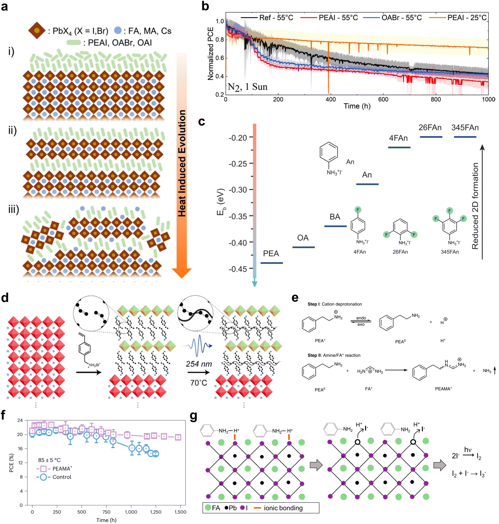 | ||
| Fig. 9 (a) Scheme of the evolution of the 2D/3D heterostructure treated with bulky cations upon annealing. (b) The maximum power point tracking of different 2D/3D devices measured under various temperatures.140 Reproduced with permission.140 Copyright 2022, John Wiley and Sons. (c) Binding energy calculated for ammonium ligands substituted into MAPbI3 perovskite slabs and the structure of aniliniums.143 Reproduced with permission.143 Copyright 2022, The American Association for the Advancement of Science. (d) Scheme of the formation process of cross-linked 2D perovskite on top of the 3D phase using VBA cations.144 Reproduced with permission.144 Copyright 2019, American Chemical Society. (e) Chemical reactions between PEA+ and FA+. Reproduced with permission.145 Copyright 2023, Springer Nature. (f) The device stability of control and PEAMA+ devices measured under 85 °C and 1 sun illumination.145 (g) Chemical reaction between the perovskite surface and anilinium.146 Reproduced with permission.146 Copyright 2021, American Chemical Society. | ||
Due to the intercalation and reconstruction issue of 2D/3D heterojunctions under thermal stress, especially with an 85 °C thermal stability test, other ammonium passivators have been developed to avoid the formation of 2D perovskite phases, such as the fluorinated aniliniums (Fig. 9(c)).143,147 It has been reported that tuning the substitution site of PDEAI2 gives different formation energies of DJ-phase 2D perovskites.147 The one with the greatest steric hindrance, ortho-PDEAI2, has the smallest tendency to form a DJ-phase 2D perovskite, preventing the ligand from entering the perovskite lattice, showing excellent passivation effects and enhanced stability, better than para-PDEAI2 which is prone to forming a traditional DJ-phase 2D phase. Other methods have also been adopted to inhibit ion diffusion across the interfaces through inserting cross-linked polymers between 2D and 3D phases.148 However, these strategies diminish the important advantages of tuning energy level alignment through 2D/3D heterojunctions. New types of 2D-phase ligands are required to inhibit the reconstruction of the perovskite surface during the thermal aging process. For example, the photochemically cross-linked 2D/3D heterojunction, formed with a 4-vinylbenzylammonium (VBA) ligand, could be a promising candidate to suppress ion migration during the aging process (Fig. 9(d)).144 The ligands were connected into an in-plane polymer chain structure after the 2D perovskite was formed, which could impede the diffusion of small ligands. The steric organic ammonium salt, nortropinone iodide, was also introduced to the interface, increasing the steric hindrance to migration, but through forming a 1D/3D heterojunction instead of a 2D/3D structure.149 A secondary amine has also been used to form a 2D/3D heterostructure, which exhibited improved thermal stability due to the strong intermolecular interactions, although more crystallographic studies have to be performed to confirm the structures.150 The conjugated ligands have been demonstrated to significantly suppress anion migration in a 2D perovskite, in out-of-plane and in-plane directions.151–153 With their bulky size and steric hindrance effect, they are expected to impede the reconstruction of the 2D/3D heterojunction, but can still be designed to form stable 2D perovskites with excellent electronic properties, which are excellent candidates for ligands to solve stability issues.
Another new degradation mechanism induced by a 2D/3D heterostructure is the degradation of the organic ligand itself. With the development of FAPbI3-based PSCs, the reaction between FA+ cations and ligands becomes an issue. The reaction between an FA+ cation and 3-AMPY to form MPyFA+ (N-(3-methylpyridine) formamidinium) was first used as a passivation strategy to smooth the surface energy levels of 3D perovskite thin films.99 However, the reaction was later found also to occur between FA+ cations and commonly used 2D-phase ligands, such as PEA+ and BA+ at 85 °C under illumination.145 Ligands with a low acid dissociation constant (pKa) can easily be deprotonated and react with FA+ cations, forming methaniminium and releasing ammonia (Fig. 9(e)), which damages the perovskite surfaces and grain boundaries, severely limiting the high-temperature photostability of these 2D/3D PSCs. New ammonium cations with high pKa were developed through directly adopting (phenethylamino)methaniminium (PEAMA+, pKa = 12.0) as a passivation ligand, enhancing the thermal stability of the device (Fig. 9(f)). The pKa values of a diversity of other ammonium cations have been investigated, clearly showing that cyclohexylammonium chloride (CYCl) with a pKa of 10.6 exhibited the lowest free iodide generation under illumination, the best device efficiency, and a longer lifetime (Fig. 9(g)).146 Nevertheless, not all these ammonium cations with high pKa values have been demonstrated as forming stable 2D perovskite structures.
8. Summary and outlook
Leveraging the high efficiency and good stability already achieved with 2D/3D heterostructures in PSCs, it is still going to be one of the most promising strategies for the commercialization of PSCs and will also be the important next step for the development of perovskite LEDs and photodetectors. We have discussed how the ligand configuration influences the structural characteristics in 2D/3D heterojunctions, including the phase space, the thickness of the inorganic perovskite layer, the orientation of the 2D perovskite and the morphology of the 2D/3D heterojunction. We have also systematically reviewed the photophysics at 2D/3D heterojunctions, including the influencing factors and modulation of the carrier dynamics through ligand configurations, which pave the way for efficient device applications. An understanding of structural and photophysical characteristics directly impacts the device performance when these heterostructures are adopted into solar cells, light-emitting devices or photodetectors. A vast number of reports have shown the advantages of 2D/3D heterojunctions in devices, which improve efficiencies and stabilities through passivating trap states, managing energy level alignments and suppressing ion migration. While the representative strategies have been reviewed, we raised awareness of current problems encountered in the device applications because of the unclear degradation mechanism and arguable stability. Here we briefly propose a few research directions that need further investigation and development to set solid foundations for future stable and efficient PSCs:(1) As theoretical calculations have demonstrated the critical role of an atomic-scale interfacial chemical environment for the energy alignment of a 2D/3D heterojunction, there is a desire to develop advanced characterization techniques to probe it experimentally. Influencing factors include but are not limited to the termination plane of the 3D perovskite, amount of ligands inserted at interfaces, and ligand cation dipole. Omissions in considering all these factors could be one of the causes for the discrepancies in the type of energy alignment existing in 2D/3D heterojunctions. Building a framework that can predict the interfacial energy alignment with consideration of all these factors, will not only unify the current energy alignment model but also lead to surface pretreatment to modulate the surface chemical environment and support the future design of new ligands.
(2) 2D/3D heterojunctions are mainly built on the top of 3D perovskite thin films, owing to the relative ease of the surface treatment process. However, the microstructures and energy alignment at the bottom interfaces proved their importance in the efficiency and stability of PSCs.154–156 The creation of 2D/3D heterojunctions at the bottom interfaces began to unlock their potential in the field.29,54 However, it remains challenging to develop a non-disruptive method to grow a 3D perovskite on top of 2D crystals with high qualities. Thermal evaporation for 3D thin film growth is one strategy, but it diminishes the advantage of low cost with a solution process. Given the enormous opportunities organic molecules offer and their roles in manipulating the crystallization process of 3D perovskites, new design rules will emerge to generate new types of ligand which either spontaneously form 2D structures at the bottom during the global crystallization process of 3D perovskite, or avoid dissolution by a solvent during the growth of the 3D phase.
(3) With the emphasis on the stability of PSCs, previously hidden problems of 2D/3D heterojunctions are brought to the surface, and new ligand designs will be needed to solve those problems. As mentioned before, the dynamic nature of 2D/3D heterostructures causes reconstruction and degradation during thermal and illumination aging processes. The new types of ligand that have high pKa to reduce the reactivity and low penetration depth to avoid migration, will guide the field to achieve significantly improved device stability, while still maintaining the energy alignment benefit of 2D/3D heterojunctions.
(4) Fully exploring the potential of conjugated ligands may be leveraged to tune the structural and optoelectronic properties of 2D perovskites. Conjugated ligands are a special group of ligands that directly participate in the energy alignment of 2D perovskites, instead of regulating the inorganic layers, which gives it a wider window in changing optoelectronic properties. While the current strategy controls the n-phases of the 2D structures to reduce the electron-transporting barriers at interfaces between the perovskite and the electron-transporting layer in inverted device structures, the conjugated ligands may have the capability of diminishing the energy barrier and changing it to reverse type-II alignment to facilitate electron transport at these interfaces. The bulkiness and the rigidness of conjugated ligands will also easily regulate the lattice distortion and formation energy of 2D perovskites, consequently controlling the growth kinetics and morphology of 2D/3D heterostructures. The current challenge for widespread application of this strategy is the synthetic difficulties that require an easy pathway. A machine-learning algorithm will emerge and reduce the workload of organic synthesis, guiding further exploration.
(5) Expanding the library of 2D perovskite materials and structures will be another avenue towards engineering 2D/3D interface energy levels and other carrier dynamics properties. The surface treatment strategy of 2D/3D heterostructure developed from cation exchange with ligand solutions to the full precursor solution or vapor phase deposition methods, which enabled more possibilities for compositional and structural modulation of capping 2D perovskites. For example, incorporating metal cations other than Pb2+/Sn2+ allowed stronger n–N isotype heterojunctions and improved the built-in potential.22 Introducing an all-inorganic 2D perovskite structure into all-inorganic perovskite solar cells created a new type of 2D/3D heterojunction and provided extraordinary stability performance.134 With the discovery of other stable facets,157 corresponding 2D perovskites suited for different facets may also need to be developed to catch up with the conventional (100) facet, and a new group of bulky organic ligands will be desirable.
In summary, a comprehensive understanding of the atomic-level structure of a 2D/3D heterojunction will mature the strategy, and continued research and advances in new ligand configurations to fulfill more desires will guide the field to achieve high-performance devices in terms of efficiency and stability.
Author contributions
Writing and editing of the manuscript: K. M. and J. S. Supervision: L. D. and K. M.Data availability
No primary research results, software or code have been included, and no new data were generated or analysed as part of this review.Conflicts of interest
There are no conflicts to declare.Acknowledgements
The authors acknowledge funding support from the Solar Energy Technologies Office under the U.S. Department of Energy with the Award DE-EE0009519.Notes and references
- A. Kojima, K. Teshima, Y. Shirai and T. Miyasaka, J. Am. Chem. Soc., 2009, 131, 6050–6051 CrossRef CAS PubMed
.
- Z. Li, B. Li, X. Wu, S. A. Sheppard, S. Zhang, D. Gao, N. J. Long and Z. Zhu, Science, 2022, 376, 416–420 CrossRef CAS PubMed
- J. Suo, B. Yang, E. Mosconi, D. Bogachuk, T. A. S. Doherty, K. Frohna, D. J. Kubicki, F. Fu, Y. Kim, O. Er-Raji, T. Zhang, L. Baldinelli, L. Wagner, A. N. Tiwari, F. Gao, A. Hinsch, S. D. Stranks, F. De Angelis and A. Hagfeldt, Nat. Energy, 2024, 9, 172–183 CrossRef CAS PubMed
- R. Lin, Y. Wang, Q. Lu, B. Tang, J. Li, H. Gao, Y. Gao, H. Li, C. Ding, J. Wen, P. Wu, C. Liu, S. Zhao, K. Xiao, Z. Liu, C. Ma, Y. Deng, L. Li, F. Fan and H. Tan, Nature, 2023, 620, 994–1000 CrossRef CAS PubMed
- J. Park, J. Kim, H.-S. Yun, M. J. Paik, E. Noh, H. J. Mun, M. G. Kim, T. J. Shin and S. Il Seok, Nature, 2023, 616, 724–730 CrossRef CAS PubMed
- O. Almora, D. Baran, G. C. Bazan, C. I. Cabrera, S. Erten-Ela, K. Forberich, F. Guo, J. Hauch, A. W. Y. Ho-Baillie, T. J. Jacobsson, R. A. J. Janssen, T. Kirchartz, N. Kopidakis, M. A. Loi, R. R. Lunt, X. Mathew, M. D. Mcgehee, J. Min, D. B. Mitzi, M. K. Nazeeruddin, J. Nelson, A. F. Nogueira, U. W. Paetzold, B. P. Rand, U. Rau, H. J. Snaith, E. Unger, L. Vaillant-Roca, C. Yang, H. Yip and C. J. Brabec, Adv. Energy Mater., 2023, 13, 2203313 CrossRef CAS
- J.-W. Lee, S. Tan, S. Il Seok, Y. Yang and N.-G. Park, Science, 2022, 375, eabj1186 CrossRef CAS PubMed
- D. Luo, R. Su, W. Zhang, Q. Gong and R. Zhu, Nat. Rev. Mater., 2020, 5, 44–60 CrossRef CAS
- Z. Ni, C. Bao, Y. Liu, Q. Jiang, W.-Q. Wu, S. Chen, X. Dai, B. Chen, B. Hartweg, Z. Yu, Z. Holman and J. Huang, Science, 2020, 367, 1352–1358 CrossRef CAS PubMed
- Y. Xia, C. Zhao, P. Zhao, L. Mao, Y. Ding, D. Hong, Y. Tian, W. Yan and Z. Jin, J. Power Sources, 2021, 494, 229781 CrossRef CAS
- L. Qin, M. Zhu, Y. Xia, X. Ma, D. Hong, Y. Tian, Z. Tie and Z. Jin, Nano Res., 2024, 17, 5131–5137 CrossRef CAS
- G. Grancini and M. K. Nazeeruddin, Nat. Rev. Mater., 2019, 4, 4–22 CrossRef CAS
- L. Mao, C. C. Stoumpos and M. G. Kanatzidis, J. Am. Chem. Soc., 2019, 141, 1171–1190 CrossRef CAS PubMed
- F. Zhang, H. Lu, J. Tong, J. J. Berry, M. C. Beard and K. Zhu, Energy Environ. Sci., 2020, 13, 1154–1186 RSC
- X. Zhao, T. Liu and Y. Loo, Adv. Mater., 2022, 34, 2105849 CrossRef CAS PubMed
- T.-H. Han, K. Y. Jang, Y. Dong, R. H. Friend, E. H. Sargent and T.-W. Lee, Nat. Rev. Mater., 2022, 7, 757–777 CrossRef
- J. Yan, W. Qiu, G. Wu, P. Heremans and H. Chen, J. Mater. Chem. A, 2018, 6, 11063–11077 RSC
- P. Gao, A. R. Bin Mohd Yusoff and M. K. Nazeeruddin, Nat. Commun., 2018, 9, 5028 CrossRef PubMed
- W. Huang, Y. Wang and S. K. Balakrishnan, Chem. Commun., 2018, 54, 7944–7947 RSC
- B. Singh, N. G. Saykar, B. S. Kumar, D. Afria, C. K. Sangeetha and S. R. Rondiya, ACS Omega, 2024, 9, 10000–10016 CrossRef CAS PubMed
- S. Ramakrishnan, D. Song, Y. Xu, X. Zhang, G. Aksoy, M. Cotlet, M. Li, Y. Zhang and Q. Yu, Adv. Energy Mater., 2023, 13, 2302240 CrossRef CAS
- S. Ye, H. Rao, M. Feng, L. Xi, Z. Yen, D. H. L. Seng, Q. Xu, C. Boothroyd, B. Chen, Y. Guo, B. Wang, T. Salim, Q. Zhang, H. He, Y. Wang, X. Xiao, Y. M. Lam and T. C. Sum, Nat. Energy, 2023, 8, 284–293 CrossRef CAS
- H. Chen, S. Teale, B. Chen, Y. Hou, L. Grater, T. Zhu, K. Bertens, S. M. Park, H. R. Atapattu, Y. Gao, M. Wei, A. K. Johnston, Q. Zhou, K. Xu, D. Yu, C. Han, T. Cui, E. H. Jung, C. Zhou, W. Zhou, A. H. Proppe, S. Hoogland, F. Laquai, T. Filleter, K. R. Graham, Z. Ning and E. H. Sargent, Nat. Photonics, 2022, 16, 352–358 CrossRef CAS
- S. Sidhik, Y. Wang, M. De Siena, R. Asadpour, A. J. Torma, T. Terlier, K. Ho, W. Li, A. B. Puthirath, X. Shuai, A. Agrawal, B. Traore, M. Jones, R. Giridharagopal, P. M. Ajayan, J. Strzalka, D. S. Ginger, C. Katan, M. A. Alam, J. Even, M. G. Kanatzidis and A. D. Mohite, Science, 2022, 377, 1425–1430 CrossRef CAS PubMed
- R. Azmi, E. Ugur, A. Seitkhan, F. Aljamaan, A. S. Subbiah, J. Liu, G. Harrison, M. I. Nugraha, M. K. Eswaran, M. Babics, Y. Chen, F. Xu, T. G. Allen, A. ur Rehman, C.-L. Wang, T. D. Anthopoulos, U. Schwingenschlögl, M. D. Bastiani, E. Aydin and S. D. Wolf, Science, 2022, 376(6588), 73–77 CrossRef CAS PubMed
- Q. Jiang, Y. Zhao, X. Zhang, X. Yang, Y. Chen, Z. Chu, Q. Ye, X. Li, Z. Yin and J. You, Nat. Photonics, 2019, 13, 460–466 CrossRef CAS
- Y.-W. Jang, S. Lee, K. M. Yeom, K. Jeong, K. Choi, M. Choi and J. H. Noh, Nat. Energy, 2021, 6, 63–71 CrossRef CAS
- J. Wen, Y. Zhao, P. Wu, Y. Liu, X. Zheng, R. Lin, S. Wan, K. Li, H. Luo, Y. Tian, L. Li and H. Tan, Nat. Commun., 2023, 14, 7118 CrossRef CAS PubMed
- R. Azmi, D. S. Utomo, B. Vishal, S. Zhumagali, P. Dally, A. M. Risqi, A. Prasetio, E. Ugur, F. Cao, I. F. Imran, A. A. Said, A. R. Pininti, A. S. Subbiah, E. Aydin, C. Xiao, S. Il Seok and S. De Wolf, Nature, 2024, 628, 93–98 CrossRef CAS PubMed
- J.-C. Blancon, J. Even, C. C. Stoumpos, M. G. Kanatzidis and A. D. Mohite, Nat. Nanotechnol., 2020, 15, 969–985 CrossRef CAS PubMed
- E. S. Vasileiadou, B. Wang, I. Spanopoulos, I. Hadar, A. Navrotsky and M. G. Kanatzidis, J. Am. Chem. Soc., 2021, 143, 2523–2536 CrossRef CAS PubMed
- I. Zimmermann, S. Aghazada and M. K. Nazeeruddin, Angew. Chem., Int. Ed., 2019, 58, 1072–1076 CrossRef CAS PubMed
- H. Gao, W. Wei, L. Li, Y. Tan and Y. Tang, J. Phys. Chem. C, 2020, 124, 19204–19211 CrossRef CAS
- Y. Lei, Y. Li, C. Lu, Q. Yan, Y. Wu, F. Babbe, H. Gong, S. Zhang, J. Zhou, R. Wang, R. Zhang, Y. Chen, H. Tsai, Y. Gu, H. Hu, Y.-H. Lo, W. Nie, T. Lee, J. Luo, K. Yang, K.-I. Jang and S. Xu, Nature, 2022, 608, 317–323 CrossRef CAS PubMed
- D. Pan, Y. Fu, N. Spitha, Y. Zhao, C. R. Roy, D. J. Morrow, D. D. Kohler, J. C. Wright and S. Jin, Nat. Nanotechnol., 2021, 16, 159–165 CrossRef CAS PubMed
- A. Dučinskas, G. Y. Kim, D. Moia, A. Senocrate, Y.-R. Wang, M. A. Hope, A. Mishra, D. J. Kubicki, M. Siczek, W. Bury, T. Schneeberger, L. Emsley, J. V. Milić, J. Maier and M. Grätzel, ACS Energy Lett., 2021, 6, 337–344 CrossRef
- J. Y. Park, R. Song, J. Liang, L. Jin, K. Wang, S. Li, E. Shi, Y. Gao, M. Zeller, S. J. Teat, P. Guo, L. Huang, Y. S. Zhao, V. Blum and L. Dou, Nat. Chem., 2023, 15, 1745–1753 CrossRef CAS PubMed
- K. Ma, J. Sun, H. R. Atapattu, B. W. Larson, H. Yang, D. Sun, K. Chen, K. Wang, Y. Lee, Y. Tang, A. Bhoopalam, L. Huang, K. R. Graham, J. Mei and L. Dou, Sci. Adv., 2023, 9, eadg0032 CrossRef CAS PubMed
- Q. Wei, F. Zhang, X. Li, F. Wu, Z. Yue, J. Luo and X. Liu, Small, 2024, 2311969 CrossRef PubMed
- X. Zhao, M. L. Ball, A. Kakekhani, T. Liu, A. M. Rappe and Y.-L. Loo, Nat. Commun., 2022, 13, 3970 CrossRef CAS PubMed
- P. Li, Y. Zhang, C. Liang, G. Xing, X. Liu, F. Li, X. Liu, X. Hu, G. Shao and Y. Song, Adv. Mater., 2018, 30, 1805323 CrossRef PubMed
- C. Gong, X. Chen, J. Zeng, H. Wang, H. Li, Q. Qian, C. Zhang, Q. Zhuang, X. Yu, S. Gong, H. Yang, B. Xu, J. Chen and Z. Zang, Adv. Mater., 2024, 36, 2307422 CrossRef CAS PubMed
- M. Xiong, W. Zou, K. Fan, C. Qin, S. Li, L. Fei, J. Jiang, H. Huang, L. Shen, F. Gao, A. K.-Y. Jen and K. Yao, ACS Energy Lett., 2022, 7, 550–559 CrossRef CAS
- K. Wang, Z.-Y. Lin, Z. Zhang, L. Jin, K. Ma, A. H. Coffey, H. R. Atapattu, Y. Gao, J. Y. Park, Z. Wei, B. P. Finkenauer, C. Zhu, X. Meng, S. N. Chowdhury, Z. Chen, T. Terlier, T.-H. Do, Y. Yao, K. R. Graham, A. Boltasseva, T.-F. Guo, L. Huang, H. Gao, B. M. Savoie and L. Dou, Nat. Commun., 2023, 14, 397 CrossRef CAS PubMed
- S. J. Yang, K. Wang, Y. Luo, J. Y. Park, H. Yang, A. H. Coffey, K. Ma, J. Sun, S. Wieghold, C. Zhu and L. Dou, ACS Energy Lett., 2023, 8, 3693–3701 CrossRef CAS
- J. Seo, K. Wang, A. H. Coffey, G. He, H. Yang, Y. H. Lee, K. Ma, J. Sun, J. Y. Park, H. Zhao, C. Yuan, C. Zhu, M. Y. Sfeir and L. Dou, Adv. Opt. Mater., 2023, 11, 2301164 CrossRef CAS
- G. Uzurano, N. Kuwahara, T. Saito, A. Fujii and M. Ozaki, ACS Mater. Lett., 2022, 4, 378–384 CrossRef CAS
- G. Uzurano, N. Kuwahara, T. Saito, K. Abe, S. Miyake, D. Hishida, Y. Takeoka, A. Fujii and M. Ozaki, Appl. Phys. Express, 2023, 16, 41005 CrossRef
- M. E. F. Bouduban, V. I. E. Queloz, V. M. Caselli, K. T. Cho, A. R. Kirmani, S. Paek, C. Roldan-Carmona, L. J. Richter, J. E. Moser, T. J. Savenije, M. K. Nazeeruddin and G. Grancini, J. Phys. Chem. Lett., 2019, 10, 5713–5720 CrossRef CAS PubMed
- T. Niu, J. Lu, X. Jia, Z. Xu, M.-C. Tang, D. Barrit, N. Yuan, J. Ding, X. Zhang, Y. Fan, T. Luo, Y. Zhang, D.-M. Smilgies, Z. Liu, A. Amassian, S. Jin, K. Zhao and S. Liu, Nano Lett., 2019, 19, 7181–7190 CrossRef CAS PubMed
- Z. Zhu, C. Zhu, L. Yang, Q. Chen, L. Zhang, J. Dai, J. Cao, S. Zeng, Z. Wang, Z. Wang, W. Zhang, J. Bao, L. Yang, Y. Yang, B. Chen, C. Yin, H. Chen, Y. Cao, H. Gu, J. Yan, N. Wang, G. Xing, H. Li, X. Wang, S. Li, Z. Liu, H. Zhang, L. Wang, X. Huang and W. Huang, Nat. Mater., 2022, 21, 1042–1049 CrossRef CAS PubMed
- A. H. Proppe, A. Johnston, S. Teale, A. Mahata, R. Quintero-Bermudez, E. H. Jung, L. Grater, T. Cui, T. Filleter, C.-Y. Kim, S. O. Kelley, F. De Angelis and E. H. Sargent, Nat. Commun., 2021, 12, 3472 CrossRef CAS PubMed
- J. Sun, K. Ma, Z.-Y. Lin, Y. Tang, D. Varadharajan, A. X. Chen, H. R. Atapattu, Y. H. Lee, K. Chen, B. W. Boudouris, K. R. Graham, D. J. Lipomi, J. Mei, B. M. Savoie and L. Dou, Adv. Mater., 2023, 35, 2300647 CrossRef CAS PubMed
- H. Li, C. Zhang, C. Gong, D. Zhang, H. Zhang, Q. Zhuang, X. Yu, S. Gong, X. Chen, J. Yang, X. Li, R. Li, J. Li, J. Zhou, H. Yang, Q. Lin, J. Chu, M. Grätzel, J. Chen and Z. Zang, Nat. Energy, 2023, 8, 946–955 CrossRef CAS
- H. Zhang, L. Pfeifer, S. M. Zakeeruddin, J. Chu and M. Grätzel, Nat. Rev. Chem., 2023, 7, 632–652 CrossRef CAS PubMed
- F. Yao and Q. Lin, ACS Photonics, 2022, 9, 3165–3171 CrossRef CAS
- Z. Yang, J. Lai, R. Zhu, J. Tan, Y. Luo and S. Ye, J. Phys. Chem. C, 2022, 126, 12689–12695 CrossRef CAS
- M. Zhang, Y. Sun, X. Wang, J. Gao, H.-Y. Wang, J. Lin, Y. Wang, L.-M. Fu, X.-C. Ai and J.-P. Zhang, J. Phys. Chem. Lett., 2023, 14, 1934–1940 CrossRef CAS PubMed
- D. W. deQuilettes, J. J. Yoo, R. Brenes, F. U. Kosasih, M. Laitz, B. D. Dou, D. J. Graham, K. Ho, Y. Shi, S. S. Shin, C. Ducati, M. G. Bawendi and V. Bulović, Nat. Energy, 2024, 9, 457–466 CrossRef CAS
- W. Yang, B. Ding, Z. Lin, J. Sun, Y. Meng, Y. Ding, J. Sheng, Z. Yang, J. Ye, P. J. Dyson and M. K. Nazeeruddin, Adv. Mater., 2023, 35, 2302071 CrossRef CAS PubMed
- F. Zhang, S. Y. Park, C. Yao, H. Lu, S. P. Dunfield, C. Xiao, S. Uličná, X. Zhao, L. D. Hill, X. Chen, X. Wang, L. E. Mundt, K. H. Stone, L. T. Schelhas, G. Teeter, S. Parkin, E. L. Ratcliff, Y.-L. Loo, J. J. Berry, M. C. Beard, Y. Yan, B. W. Larson and K. Zhu, Science, 2021, 375(6576), 71–76 CrossRef PubMed
- T. Zhang, M. Long, M. Qin, X. Lu, S. Chen, F. Xie, L. Gong, J. Chen, M. Chu, Q. Miao, Z. Chen, W. Xu, P. Liu, W. Xie and J. Xu, Joule, 2018, 2, 2706–2721 CrossRef CAS
- T. Yang, F. Li, C.-H. Lin, X. Guan, Y. Yao, X. Yang, T. Wu and R. Zheng, Cell Rep. Phys. Sci., 2023, 4, 101447 CrossRef CAS
- C. Li, R. Zhu, Z. Yang, J. Lai, J. Tan, Y. Luo and S. Ye, Angew. Chem., 2023, 135, e202214208 CrossRef
- M.-Y. Kuo, N. Spitha, M. P. Hautzinger, P.-L. Hsieh, J. Li, D. Pan, Y. Zhao, L.-J. Chen, M. H. Huang, S. Jin, Y.-J. Hsu and J. C. Wright, J. Am. Chem. Soc., 2021, 143, 4969–4978 CrossRef CAS PubMed
- R. Quintero-Bermudez, A. H. Proppe, A. Mahata, P. Todorović, S. O. Kelley, F. De Angelis and E. H. Sargent, J. Am. Chem. Soc., 2019, 141, 13459–13467 CrossRef CAS PubMed
- A. Mahata, E. Mosconi, D. Meggiolaro and F. De Angelis, Chem. Mater., 2020, 32, 105–113 CrossRef CAS
- J. Li, J. Ma, X. Cheng, Z. Liu, Y. Chen and D. Li, ACS Nano, 2020, 14, 2156–2161 CrossRef CAS PubMed
- H. Duim, H.-H. Fang, S. Adjokatse, G. H. ten Brink, M. A. L. Marques, B. J. Kooi, G. R. Blake, S. Botti and M. A. Loi, Appl. Phys. Rev., 2019, 6, 31401 Search PubMed
- B. Traoré, P. Basera, A. J. Ramadan, H. J. Snaith, C. Katan and J. Even, ACS Energy Lett., 2022, 7, 349–357 CrossRef
- W. Li, S. Sidhik, B. Traore, R. Asadpour, J. Hou, H. Zhang, A. Fehr, J. Essman, Y. Wang, J. M. Hoffman, I. Spanopoulos, J. J. Crochet, E. Tsai, J. Strzalka, C. Katan, M. A. Alam, M. G. Kanatzidis, J. Even, J.-C. Blancon and A. D. Mohite, Nat. Nanotechnol., 2022, 17, 45–52 CrossRef CAS PubMed
- D. Yu, F. Cao, J. Liao, B. Wang, C. Su and G. Xing, Nat. Commun., 2022, 13, 6229 CrossRef CAS PubMed
- K. Wei, T. Jiang, Z. Xu, J. Zhou, J. You, Y. Tang, H. Li, R. Chen, X. Zheng, S. Wang, K. Yin, Z. Wang, J. Wang and X. Cheng, Laser Photonics Rev., 2018, 12, 1800128 CrossRef
- P. Li, X. Liu, Y. Zhang, C. Liang, G. Chen, F. Li, M. Su, G. Xing, X. Tao and Y. Song, Angew. Chem., 2020, 132, 6976–6981 CrossRef
- Y. Dong, X. Dong, D. Lu, M. Chen, N. Zheng, R. Wang, Q. Li, Z. Xie and Y. Liu, Adv. Mater., 2022, 35, 2205258 CrossRef PubMed
- T. Sheikh, V. Nawale, N. Pathoor, C. Phadnis, A. Chowdhury and A. Nag, Angew. Chem., Int. Ed., 2020, 59, 11653 CrossRef CAS PubMed
- F. Zhang, D. H. Kim, H. Lu, J.-S. Park, B. W. Larson, J. Hu, L. Gao, C. Xiao, O. G. Reid, X. Chen, Q. Zhao, P. F. Ndione, J. J. Berry, W. You, A. Walsh, M. C. Beard and K. Zhu, J. Am. Chem. Soc., 2019, 141, 5972–5979 CrossRef CAS PubMed
- J. Hu, I. W. H. Oswald, S. J. Stuard, M. M. Nahid, N. Zhou, O. F. Williams, Z. Guo, L. Yan, H. Hu, Z. Chen, X. Xiao, Y. Lin, Z. Yang, J. Huang, A. M. Moran, H. Ade, J. R. Neilson and W. You, Nat. Commun., 2019, 10, 1276 CrossRef PubMed
- J. Sun, K. Wang, K. Ma, J. Y. Park, Z.-Y. Lin, B. M. Savoie and L. Dou, J. Am. Chem. Soc., 2023, 145, 20694–20715 CrossRef CAS PubMed
- Y. Gao, E. Shi, S. Deng, S. B. Shiring, J. M. Snaider, C. Liang, B. Yuan, R. Song, S. M. Janke, A. Liebman-Peláez, P. Yoo, M. Zeller, B. W. Boudouris, P. Liao, C. Zhu, V. Blum, Y. Yu, B. M. Savoie, L. Huang and L. Dou, Nat. Chem., 2019, 11, 1151–1157 CrossRef CAS PubMed
- Y. Gao, Z. Wei, P. Yoo, E. Shi, M. Zeller, C. Zhu, P. Liao and L. Dou, J. Am. Chem. Soc., 2019, 141, 15577–15585 CrossRef CAS PubMed
- E. Shi, S. Deng, B. Yuan, Y. Gao, Akriti, L. Yuan, C. S. Davis, D. Zemlyanov, Y. Yu, L. Huang and L. Dou, ACS Nano, 2019, 13, 1635–1644 CrossRef CAS PubMed
- Z. Wei, K. Wang, W. Zhao, Y. Gao, Q. Hu, K. Chen and L. Dou, Chem. Commun., 2021, 57, 11469–11472 RSC
- S. Deng, J. M. Snaider, Y. Gao, E. Shi, L. Jin, R. D. Schaller, L. Dou and L. Huang, J. Chem. Phys., 2020, 152, 44711 CrossRef CAS PubMed
- J. V. Passarelli, D. J. Fairfield, N. A. Sather, M. P. Hendricks, H. Sai, C. L. Stern and S. I. Stupp, J. Am. Chem. Soc., 2018, 140, 7313–7323 CrossRef CAS PubMed
- J. V. Passarelli, C. M. Mauck, S. W. Winslow, C. F. Perkinson, J. C. Bard, H. Sai, K. W. Williams, A. Narayanan, D. J. Fairfield, M. P. Hendricks, W. A. Tisdale and S. I. Stupp, Nat. Chem., 2020, 12, 672–682 CrossRef CAS PubMed
- W. T. M. Van Gompel, R. Herckens, K. Van Hecke, B. Ruttens, J. D’Haen, L. Lutsen and D. Vanderzande, Chem. Commun., 2019, 55, 2481–2484 RSC
- Y. Xia, M. Zhu, L. Qin, C. Zhao, D. Hong, Y. Tian, W. Yan and Z. Jin, Energy Mater., 2023, 3, 300004 CrossRef CAS
- Q. Zhuang, H. Li, C. Zhang, C. Gong, H. Yang, J. Chen and Z. Zang, Adv. Mater., 2023, 35, 2303275 CrossRef CAS PubMed
- Z. Chen, X. Zheng, F. Yao, J. Ma, C. Tao and G. Fang, J. Mater. Chem. A, 2018, 6, 17625–17632 RSC
- M. D. Malouangou, Y. Yang, Y. Zhang, L. Bai, J. T. Matondo, M. Mbumba, M. W. Akram and M. Guli, Mater. Res. Bull., 2022, 150, 111793 CrossRef CAS
- L. Mao, W. Ke, L. Pedesseau, Y. Wu, C. Katan, J. Even, M. R. Wasielewski, C. C. Stoumpos and M. G. Kanatzidis, J. Am. Chem. Soc., 2018, 140, 3775–3783 CrossRef CAS PubMed
- M. Chen, M.-G. Ju, M. Hu, Z. Dai, Y. Hu, Y. Rong, H. Han, X. C. Zeng, Y. Zhou and N. P. Padture, ACS Energy Lett., 2019, 4, 276–277 CrossRef CAS
- S. Wu, J. Zhang, Z. Li, D. Liu, M. Qin, S. H. Cheung, X. Lu, D. Lei, S. K. So, Z. Zhu and A. K.-Y. Jen, Joule, 2020, 4, 1248–1262 CrossRef CAS
- X. Jiang, J. Zhang, S. Ahmad, D. Tu, X. Liu, G. Jia, X. Guo and C. Li, Nano Energy, 2020, 75, 104892 CrossRef CAS
- J. Lu, L. Jiang, W. Li, F. Li, N. K. Pai, A. D. Scully, C.-M. Tsai, U. Bach, A. N. Simonov, Y.-B. Cheng and L. Spiccia, Adv. Energy Mater., 2017, 7, 1700444 CrossRef
- T. Yang, C. Ma, W. Cai, S. Wang, Y. Wu, J. Feng, N. Wu, H. Li, W. Huang, Z. Ding, L. Gao, S. (Frank) Liu and K. Zhao, Joule, 2023, 7, 574–586 CrossRef CAS
- Y. Zhong, G. Liu, Y. Su, W. Sheng, L. Gong, J. Zhang, L. Tan and Y. Chen, Angew. Chem., Int. Ed., 2022, 61, e202114588 CrossRef CAS PubMed
- Q. Jiang, J. Tong, Y. Xian, R. A. Kerner, S. P. Dunfield, C. Xiao, R. A. Scheidt, D. Kuciauskas, X. Wang, M. P. Hautzinger, R. Tirawat, M. C. Beard, D. P. Fenning, J. J. Berry, B. W. Larson, Y. Yan and K. Zhu, Nature, 2022, 611, 278–283 CrossRef CAS PubMed
- Y. Liu, S. Akin, L. Pan, R. Uchida, N. Arora, J. V. Milić, A. Hinderhofer, F. Schreiber, A. R. Uhl, S. M. Zakeeruddin, A. Hagfeldt, M. I. Dar and M. Grätzel, Sci. Adv., 2019, 5, eaaw2543 CrossRef CAS PubMed
- Y. Yan, S. Yu, A. Honarfar, T. Pullerits, K. Zheng and Z. Liang, Adv. Sci., 2019, 6, 1900548 CrossRef PubMed
- Z.-Y. Lin, J. Sun, S. B. Shiring, L. Dou and B. M. Savoie, Angew. Chem., Int. Ed., 2023, 62, e202305298 CrossRef CAS PubMed
- K. Ma, H. R. Atapattu, Q. Zhao, Y. Gao, B. P. Finkenauer, K. Wang, K. Chen, S. M. Park, A. H. Coffey, C. Zhu, L. Huang, K. R. Graham, J. Mei and L. Dou, Adv. Mater., 2021, 33, 2100791 CrossRef CAS PubMed
- S. Zhao, M. Qin, H. Wang, J. Xie, F. Xie, J. Chen, X. Lu, K. Yan and J. Xu, Sol. RRL, 2020, 4, 2000282 CrossRef CAS
- J. Xue, R. Wang, X. Chen, C. Yao, X. Jin, K.-L. Wang, W. Huang, T. Huang, Y. Zhao, Y. Zhai, D. Meng, S. Tan, R. Liu, Z.-K. Wang, C. Zhu, K. Zhu, M. C. Beard, Y. Yan and Y. Yang, Science, 2021, 371, 636–640 CrossRef CAS PubMed
- M. Braun, W. Tuffentsammer, H. Wachtel and H. C. Wolf, Chem. Phys. Lett., 1999, 307, 373–378 CrossRef CAS
- T. Zhou, Z. Xu, R. Wang, X. Dong, Q. Fu and Y. Liu, Adv. Mater., 2022, 34, 2200705 CrossRef CAS PubMed
- S. Tan, T. Huang, I. Yavuz, R. Wang, T. W. Yoon, M. Xu, Q. Xing, K. Park, D.-K. Lee, C.-H. Chen, R. Zheng, T. Yoon, Y. Zhao, H.-C. Wang, D. Meng, J. Xue, Y. J. Song, X. Pan, N.-G. Park, J.-W. Lee and Y. Yang, Nature, 2022, 605, 268–273 CrossRef CAS PubMed
- X. Liu, T. Webb, L. Dai, K. Ji, J. A. Smith, R. C. Kilbride, M. Yavari, J. Bi, A. Ren, Y. Huang, Z. Wang, Y. Shen, G. Shao, S. J. Sweeney, S. Hinder, H. Li, D. G. Lidzey, S. D. Stranks, N. C. Greenham, S. R. P. Silva and W. Zhang, Energy Environ. Mater., 2022, 5, 670–682 CrossRef
- Q. Yao, Q. Xue, Z. Li, K. Zhang, T. Zhang, N. Li, S. Yang, C. J. Brabec, H.-L. Yip and Y. Cao, Adv. Mater., 2020, 32, 2000571 CrossRef CAS PubMed
- Z. Wang, Y. Lu, Z. Xu, J. Hu, Y. Chen, C. Zhang, Y. Wang, F. Guo and Y. Mai, Adv. Sci., 2021, 8, 2101856 CrossRef CAS PubMed
- H. Kim, J. S. Kim, J.-M. Heo, M. Pei, I.-H. Park, Z. Liu, H. J. Yun, M.-H. Park, S.-H. Jeong, Y.-H. Kim, J.-W. Park, E. Oveisi, S. Nagane, A. Sadhanala, L. Zhang, J. J. Kweon, S. K. Lee, H. Yang, H. M. Jang, R. H. Friend, K. P. Loh, M. K. Nazeeruddin, N.-G. Park and T.-W. Lee, Nat. Commun., 2020, 11, 3378 CrossRef CAS PubMed
- K. Zhang, Z. Su, Y. Shen, L.-X. Cao, X.-Y. Zeng, S.-C. Feng, Y. Yu, X. Gao, J.-X. Tang and Y. Li, ACS Nano, 2024, 18, 4570–4578 CrossRef CAS PubMed
- H. Min, N. Wang, N. Chen, Y. Tong, Y. Wang, J. Wang, J. Liu, S. Wang, X. Wu, P. Yang, H. Shi, C. Zhuo, Q. Chen, J. Li, D. Zhang, X. Lu, C. Zhu, Q. Peng, L. Zhu, J. Chang, W. Huang and J. Wang, Nat. Nanotechnol., 2024, 19, 632–637 CrossRef CAS PubMed
- Y. Guo, S. Apergi, N. Li, M. Chen, C. Yin, Z. Yuan, F. Gao, F. Xie, G. Brocks, S. Tao and N. Zhao, Nat. Commun., 2021, 12, 644 CrossRef CAS PubMed
- N. Jiang, Z. Wang, Y. Zheng, Q. Guo, W. Niu, R. Zhang, F. Huang and D. Chen, Nano Energy, 2022, 97, 107181 CrossRef CAS
- T.-H. Han, J.-W. Lee, Y. J. Choi, C. Choi, S. Tan, S.-J. Lee, Y. Zhao, Y. Huang, D. Kim and Y. Yang, Adv. Mater., 2020, 32, 1905674 CrossRef CAS PubMed
- F. Zhang, B. Cai, J. Song, B. Han, B. Zhang and H. Zeng, Adv. Funct. Mater., 2020, 30, 2001732 CrossRef CAS
- Y. Fu, Q. Zhang, D. Zhang, Y. Tang, L. Shu, Y. Zhu and Z. Fan, Adv. Funct. Mater., 2020, 30, 2002913 CrossRef CAS
- Y. Li, J. Roger, I. Allegro, J. C. Fischer, Q. Jin, U. Lemmer, I. A. Howard and U. W. Paetzold, Adv. Funct. Mater., 2022, 32, 2200772 CrossRef CAS
- F. Ye, H. Zhang, P. Wang, W. Li, D. Li, B. Du, D. Liu and T. Wang, ACS Appl. Mater. Interfaces, 2019, 11, 43452–43459 CrossRef CAS PubMed
- T. Wu, Y. Yang, Y. Zou, Y. Wang, C. Wu, Y. Han, T. Song, Q. Zhang, X. Gao and B. Sun, Nanoscale, 2018, 10, 19322–19329 RSC
- L. Zhao, Y. Zhou, Z. Shi, Z. Ni, M. Wang, Y. Liu and J. Huang, Nat. Photonics, 2023, 17, 315–323 CrossRef CAS
- F. P. García De Arquer, A. Armin, P. Meredith and E. H. Sargent, Nat. Rev. Mater., 2017, 2, 16100 CrossRef
- Y. He, W. Pan, C. Guo, H. Zhang, H. Wei and B. Yang, Adv. Funct. Mater., 2021, 31, 2104880 CrossRef CAS
- Z. Xu, H. Xi, X. Sun, H. Liu, J. Liu, Y. Ba, D. Chen, G. Zhang, C. Zhang, X. Ma and Y. Hao, Adv. Funct. Mater., 2024, 2400817 CrossRef
- Z. Zhao, J. Hao, B. Jia, D. Chu, J. Pi, Y. Zhang, S. Zai, Y. Liang, Y. Li, Z. Feng, X. Zheng, M. Wei, L. Zhao, R. Shi, S. F. Liu and Y. Liu, ACS Energy Lett., 2024, 9, 2758–2766 CrossRef CAS
- D. Luo, T. Zou, W. Yang, B. Xiang, X. Yang, Y. Wang, R. Su, L. Zhao, R. Zhu, H. Zhou, T. P. Russell, H. Yu and Z. Lu, Adv. Funct. Mater., 2020, 30, 2001692 CrossRef CAS
- X. Xu, W. Qian, J. Wang, J. Yang, J. Chen, S. Xiao, Y. Ge and S. Yang, Adv. Sci., 2021, 8, 2102730 CrossRef CAS PubMed
- R. Ollearo, A. Caiazzo, J. Li, M. Fattori, A. J. J. M. van Breemen, M. M. Wienk, G. H. Gelinck and R. A. J. Janssen, Adv. Mater., 2022, 34, 2205261 CrossRef CAS PubMed
- L. Jiang, Z. Li, Q. Dong, X. Rong and G. Dong, ACS Appl. Mater. Interfaces, 2023, 15, 32647–32655 CrossRef CAS PubMed
- L. Tao, W. Tang, M. Yan, L. Ding, J. Wei, L. Wang, L. Li, L. Li, D. Yang and Y. Fang, J. Mater. Chem. C, 2023, 11, 12392–12399 RSC
- X. Zhang, L. Li, C. Ji, X. Liu, Q. Li, K. Zhang, Y. Peng, M. Hong and J. Luo, Natl. Sci. Rev., 2021, 8, nwab044 CrossRef PubMed
- X. Zhao, T. Liu, Q. C. Burlingame, T. Liu, R. Holley III, G. Cheng, N. Yao, F. Gao and Y.-L. Loo, Science, 2022, 377, 307–310 CrossRef CAS PubMed
- L. Wang, Q. Zhou, Z. Zhang, W. Li, X. Wang, Q. Tian, X. Yu, T. Sun, J. Wu, B. Zhang and P. Gao, J. Energy Chem., 2022, 64, 179–189 CrossRef CAS
- B. P. Kore, W. Zhang, B. W. Hoogendoorn, M. Safdari and J. M. Gardner, Commun. Mater., 2021, 2, 100 CrossRef CAS
- S. Kumar, L. Houben, K. Rechav and D. Cahen, Proc. Natl. Acad. Sci. U. S. A., 2022, 119, e2114740119 CrossRef CAS PubMed
- J. Chakkamalayath, N. Hiott and P. V. Kamat, ACS Energy Lett., 2023, 8, 169–171 CrossRef CAS
- G. Szabó and P. V. Kamat, ACS Energy Lett., 2024, 9, 193–200 CrossRef
- C. A. R. Perini, E. Rojas-Gatjens, M. Ravello, A. F. C. Mendez, J. Hidalgo, Y. An, S. Kim, B. Lai, R. Li, C. S. Acuña and J. Correa-Baena, Adv. Mater., 2022, 2204726 CrossRef CAS PubMed
- A. A. Sutanto, R. Szostak, N. Drigo, V. I. E. Queloz, P. E. Marchezi, J. C. Germino, H. C. N. Tolentino, M. K. Nazeeruddin, A. F. Nogueira and G. Grancini, Nano Lett., 2020, 20, 3992–3998 CrossRef CAS PubMed
- A. A. Sutanto, N. Drigo, V. I. E. Queloz, I. Garcia-Benito, A. R. Kirmani, L. Richter, P. Schouwink, K. T. Cho, S. Paek, M. K. Nazeeruddin and G. Grancini, J. Mater. Chem. A, 2020, 8, 2343–2348 RSC
- S. M. Park, M. Wei, J. Xu, H. R. Atapattu, F. T. Eickemeyer, K. Darabi, L. Grater, Y. Yang, C. Liu, S. Teale, B. Chen, H. Chen, T. Wang, L. Zeng, A. Maxwell, Z. Wang, K. R. Rao, Z. Cai, S. M. Zakeeruddin, J. T. Pham, C. M. Risko, A. Amassian, M. G. Kanatzidis, K. R. Graham, M. Grätzel and E. H. Sargent, Science, 2023, 381, 209–215 CrossRef CAS PubMed
- A. H. Proppe, M. Wei, B. Chen, R. Quintero-Bermudez, S. O. Kelley and E. H. Sargent, J. Am. Chem. Soc., 2019, 141, 14180–14189 CrossRef CAS PubMed
- M. Wang, Z. Shi, C. Fei, Z. J. D. Deng, G. Yang, S. P. Dunfield, D. P. Fenning and J. Huang, Nat. Energy, 2023, 8, 1229–1239 CrossRef CAS
- S.-H. Lee, S. Jeong, S. Seo, H. Shin, C. Ma and N.-G. Park, ACS Energy Lett., 2021, 1612–1621 CrossRef CAS
- C. Liu, Y. Yang, K. Rakstys, A. Mahata, M. Franckevicius, E. Mosconi, R. Skackauskaite, B. Ding, K. G. Brooks, O. J. Usiobo, J.-N. Audinot, H. Kanda, S. Driukas, G. Kavaliauskaite, V. Gulbinas, M. Dessimoz, V. Getautis, F. De Angelis, Y. Ding, S. Dai, P. J. Dyson and M. K. Nazeeruddin, Nat. Commun., 2021, 12, 6394 CrossRef CAS PubMed
- L. Luo, H. Zeng, Z. Wang, M. Li, S. You, B. Chen, A. Maxwell, Q. An, L. Cui, D. Luo, J. Hu, S. Li, X. Cai, W. Li, L. Li, R. Guo, R. Huang, W. Liang, Z.-H. Lu, L. Mai, Y. Rong, E. H. Sargent and X. Li, Nat. Energy, 2023, 8, 294–303 CrossRef CAS
- Y. Kang, R. Li, X. Shen, B. Jin, Y. Zhan, A. Wang, B. Li, Y. Song, G. Xiao and Q. Dong, Nano Energy, 2024, 120, 109178 CrossRef CAS
- J. Rodríguez-Romero, J. Sanchez-Diaz, C. Echeverría-Arrondo, S. Masi, D. Esparza, E. M. Barea and I. Mora-Seró, ACS Energy Lett., 2020, 5, 1013–1021 CrossRef
- E. Shi, B. Yuan, S. B. Shiring, Y. Gao, Akriti, Y. Guo, C. Su, M. Lai, P. Yang, J. Kong, B. M. Savoie, Y. Yu and L. Dou, Nature, 2020, 580, 614–620 CrossRef CAS PubMed
- Akriti, E. Shi, S. B. Shiring, J. Yang, C. L. Atencio-Martinez, B. Yuan, X. Hu, Y. Gao, B. P. Finkenauer, A. J. Pistone, Y. Yu, P. Liao, B. M. Savoie and L. Dou, Nat. Nanotechnol., 2021, 16, 584–591 CrossRef CAS PubMed
- Akriti, S. Zhang, Z.-Y. Lin, E. Shi, B. P. Finkenauer, Y. Gao, A. J. Pistone, K. Ma, B. M. Savoie and L. Dou, Adv. Mater., 2021, 33, 2105183 CrossRef CAS
- Z. Dai, S. K. Yadavalli, M. Chen, A. Abbaspourtamijani, Y. Qi and N. P. Padture, Science, 2021, 372, 618–622 CrossRef CAS PubMed
- C. Luo, G. Zheng, F. Gao, X. Wang, C. Zhan, X. Gao and Q. Zhao, Nat. Photonics, 2023, 17, 856–864 CrossRef CAS
- H. Min, D. Y. Lee, J. Kim, G. Kim, K. S. Lee, J. Kim, M. J. Paik, Y. K. Kim, K. S. Kim, M. G. Kim4, T. J. Shin and S. Il Seok, Nature, 2021, 598, 444–450 CrossRef CAS PubMed
- C. Ma, F. T. Eickemeyer, S.-H. Lee, D.-H. Kang, S. J. Kwon, M. Grätzel and N.-G. Park, Science, 2023, 379, 173–178 CrossRef CAS PubMed
| This journal is © The Royal Society of Chemistry 2024 |