
 Open Access Article
 This Open Access Article is licensed under a Creative Commons Attribution-Non Commercial 3.0 Unported Licence
A highly sensitive ion-selective chemiresistive sensor for online monitoring of lead ions in water†
Maryam
Darestani-Farahani
 a,
Isabella
Mendoza Montealegre
a,
Mehraneh
Tavakkoli Gilavan
b,
Thomas
Kirby
a,
Ponnambalam Ravi
Selvaganapathy
bc and
Peter
Kruse
*a
a,
Isabella
Mendoza Montealegre
a,
Mehraneh
Tavakkoli Gilavan
b,
Thomas
Kirby
a,
Ponnambalam Ravi
Selvaganapathy
bc and
Peter
Kruse
*a
aDepartment of Chemistry and Chemical Biology, McMaster University, 1280 Main Street West, Hamilton, Ontario L8S 4M1, Canada. E-mail: pkruse@mcmaster.ca
bSchool of Biomedical Engineering, McMaster University, 1280 Main Street West, Hamilton, Ontario L8S 4L7, Canada
cDepartment of Mechanical Engineering, McMaster University, 1280 Main Street West, Hamilton, Ontario L8S 4L7, Canada
First published on 5th April 2024
Abstract
Dissolved lead is a serious but common health hazard in drinking water, yet there is still no practical way to monitor its levels continuously in the distribution system or at the point of use. Here we propose using a lead-selective membrane on top of a chemiresistive device to continuously measure Pb2+ ion concentrations in real time. The detection limit was lowered by stabilizing the surface of the resistive film with sodium hydroxide and 15-crown-5 ether and optimizing the sensor geometry to maximize the effective surface area. The detection mechanism is based on the complexation of the Pb2+ ions by the lead ionophores within the membrane, thus modulating the interactions between the ionophores and the chemiresistive film. The limit of detection of the fabricated devices was reliably below 2 μg L−1, with concentrations up to 3 mg L−1 routinely quantifiable over several measurement cycles. The chemiresistive sensors can thus achieve lower detection limits than potentiometric devices while being more robust and simpler to fabricate by omitting the reference electrode. Ion-selective membrane-covered chemiresistors can therefore be deployed to continuously monitor drinking water sources and detect harmful levels of lead in real time.
1. Introduction
Lead continuous to be one of the most dangerous drinking water contaminants and its presence in residential areas is frequently attributed to outdated building infrastructure containing lead pipes.1 According to the World Health Organization (WHO), the maximum acceptable concentration (MAC) of lead in drinking water is 10 μg L−1.2 Exposure can come from corrosion of plumbing materials, or obtaining water from contaminated sources, as seen in Flint, Michigan.3 Currently, monitoring of lead is commonly done by random daytime sampling (RDT) which requires sample collection, treatment and inductively coupled plasma-mass spectrometry (ICP-MS), inductively coupled plasma-atomic emission spectrometry (ICP-AES), atomic adsorption spectroscopy (AAS), fluorescence or Anodic stripping voltammetry (ASV).1,4,5 These laboratory analysis techniques are time-consuming, not easily accessible, and very costly due to the instrumentation used.1Methods currently under development are optical, electrochemical and electrical sensors which are aiming to be used for in situ detection of Pb2+ in drinking water in addition to meeting the standards for a sensor such as highly accurate, precise and sensitive response.1,6–9 For instance, a type of colorimetric test strips has been commercialized by MQuant which semi-quantitatively measures Pb2+ concentration from 20 to 500 mg L−1 based on the complex formation between Rhodizonic acid and lead in acidic solutions.10 To accurately quantify lower concentrations of lead, a photometric reagent lead test kit made by Spectroquant is available on market. It can measure Pb2+ ions in a range of 10 μg L−1 to 5 mg L−1 by complex formation of Pb2+ ions with 4-(2′-pyridylazo)resorcinol (PAR) in alkaline solutions.11 Two ion-selective electrodes (ISEs) have been commercialized by Thermo Scientific (measuring 10−6 M to 0.1 M (0.2 mg L−1 to 20![[thin space (1/6-em)]](https://www.rsc.org/images/entities/char_2009.gif) 700 mg L−1) of Pb2+ in a pH range of 4–7)12 and Mettler Toledo (measuring 10−5 M to 1.0 M (2 mg L−1 to 207000 mg L−1) of Pb2+ in pH 2 to 8)13 using ion-selective membrane (ISM) technology. Although these sensors allow for fast and easy measurement of Pb2+ ions in situ, they still lack sufficient sensitivity.14
700 mg L−1) of Pb2+ in a pH range of 4–7)12 and Mettler Toledo (measuring 10−5 M to 1.0 M (2 mg L−1 to 207000 mg L−1) of Pb2+ in pH 2 to 8)13 using ion-selective membrane (ISM) technology. Although these sensors allow for fast and easy measurement of Pb2+ ions in situ, they still lack sufficient sensitivity.14
Moreover, several advanced optical and electrical Pb2+ sensors have been reported in the literature which have high sensitivity. For instance, a rapid analytical ion-sensing platform using smart hydrogels and working based on the dye release from hydrogels entrapping ion-selective microdroplets was introduced by Du et al. which was able to measure the Pb2+ concentration with a detection limit of 62 μg L−1.15 Ghosh et al. prepared an optical fiber grating functionalized with glutaraldehyde cross-linked chitosan (CCS), nitrogen-doped graphene oxide (NGO) nanocomposites, and poly(acrylic acid) (PAA). The sensor surface was modified by hydroxylation and self-assembly of CCS–NGO/PAA layers, resulting in a detection limit of 0.10 μg L−1.16 One of the main problems of optical devices is that they require reagents to react with the analyte.17 A number of electrochemical sensors for Pb2+ ions have also been reported, for example as developed by the Molinero-Abad group with a detection limit of 0.07 μg L−1. Anodic stripping voltametric method was used as a method of detection, with the surface of the working electrode modified by single-walled carbon nanotubes, electro-reduced graphene oxide and electrogenerated gold nanoparticle.18 Yu et al. modified a Pb2+-selective electrode using a conducting polymer-poly(2-methoxy-5-(2′-ethylhexyloxy)-p-phenylene vinylene) (MEH–PPV)- as an ion-to-electron transducer which resulted in a detection limit of 0.13 μg L−1.19 However, electrochemical sensors such as potentiometric ion-selective electrodes (ISE) require reference electrodes, increasing fabrication costs, and causing stability issues.20
Sensors based on field-effect transistor (FET) geometries can improve sensitivity at the expense of increased complexity.21–23 Zhou et al. developed a real-time and selective Pb2+ sensor in a FET geometry with a reduced graphene oxide (rGO) film as a semiconducting channel modified with gold nanoparticles and L-glutathione.24 It responded sensitively and selectively to Pb2+ ions in a concentration range of 10 nM to 10 μM with 11% response at 10 μM in 1 to 2 seconds. The proposed sensing mechanism was that holes of the p-doped channel are forced away from the gate insulator–semiconductor interface by the positive electrical field formed by Pb2+ ions. Thus, a depletion layer is created, resulting in a drop in current.24 Despite the high sensitivity of these solid-state devices, there are several interferants in real samples that affect their response. In addition their complicated geometry increases their cost.17
Chemiresistive sensors are solid state devices with a similar working principle to FET sensors, but a much simpler design since they operate without a gate (i.e. at zero gate voltage).25,26 They work by detecting electrical current changes across the resistive film caused by its interaction with the target analyte.27 These sensors do not require reagents, reference electrodes, or expensive instrumentation.17 However, they have not yet been successfully employed for lead detection. A reported chemiresistor with a resistive film made from β-cyclodextrin (BCD) functionalized reduced graphene oxide (rGO) has an unacceptably high limit of detection (LoD) of 10 mg L−1.28 Selectivity has also been a challenge in the development of chemiresistive devices.29,30 Recently, a new ion-selective chemiresistive platform was introduced by our group for detecting nitrate, nitrite and ammonium.31 A top layer of ion-selective membrane (ISM) simultaneously protects the sensors surfaces and enhances their selectivity.31 In order to be relevant for Pb2+ detection, the sensitivity of the platform needs to be enhanced further.
Here we demonstrate an ion-selective chemiresistive sensor capable of continuously monitoring concentrations of Pb2+ in water well below regulatory thresholds. To achieve our objective, we employed two strategies. Firstly, by modifying the resistive film with a solution of NaOH and 15-crown-5 ether to tune the electrical properties of the film and, and secondly by improving the sensor fabrication process. The device consists of a conducting CNT film coated with a Pb2+-selective membrane. The thicknesses of the conducting film (resistive film) and the membrane were optimized. Sensitivity, selectivity, stability, and reversibility of the sensors are investigated, and the sensing mechanism is discussed. Our improvements to the sensitivity and stability of the devices for detection of heavy metals make them suitable for in situ analysis, increasing the accessibility of lead testing for the general public.
2. Experimental
2.1. Materials, reagents and apparatus
Lead(II) nitrate, tris(hydroxymethyl)aminomethane, 99.7% glacial acetic acid (ACS reagent grade), single walled carbon nanotubes (6.5 chirality, ≥95% carbon nanotubes, 0.78 nm average diameter), 15-crown-5 ether, poly vinyl chloride (PVC), 2-nitrophenyl octyl ether (o-NPOE), lead ionophore IV (tert-butylcalix[4]arene-tetrakis(N,N-dimethylthioacetamide)), potassium tetrakis[3,5-bis(trifluoromethyl)phenyl]borate (KTFBP), methanol (anhydrous), acetone (ACS reagent), tetrahydrofuran (THF) were purchased from Sigma-Aldrich. Sodium hydroxide Certified A.C.S Pellets (P250–500) were purchased from Fischer Chemicals. Ultrapure water (18.2 MΩ cm) was obtained from a Millipore Simplicity 185 purification system. Acetic acid was prepared by diluting glacial acetic acid into ultrapure water.Twin frosted glass slides (75 × 25 × 1 mm3) were purchased from VWR, Carbon ink 124-39 (EU) was produced by Creative Materials Inc., ¼′′ wide adhesive copper tape (3 M #1181) purchased from 3 M. Roller, thread sealing tape (PTFE) – ½ × 520′′ and transparent adhesive Polyethylene terephthalate (PET) sheet (thickness 60 ± 8 μm) were purchased from Uline. A Cricut (Provo Craft & Novelty Inc.) low-cost cutting plotter was used to pattern the mask and the PET sheet. A gravity-fed air-brush gun (NEO for Iwata, 0.35 mm nozzle) was used with an air compressor. During the experiment, current changes were measured using EPU 452 Quad MF isoPod four channel electronics from eDAQ Pty Ltd.
For surface characterizations, SEM images were taken with JEOL 7000 Analytical SEM of airbrushed SWCNTs and f-SWCNTs on silicon/silicon dioxide (thermally grown) chips (1 × 1 cm2) with resistances similar to the sensor with an acceleration voltage of 3 kV and 10000× magnification. Hall measurements were performed with a Nanometric HL 5500PC Hall effect measurement system on Si/SiO2 chips (1 × 1 cm2) as well with four sputter coated Cr–Au contacts in van der Pauw geometry. CNTs were air brushed inside a contact mask at the center of the device with a target resistance of 9 or 10 kΩ. Raman spectra were obtained on a Renishaw inVia Raman spectrometer with a 633 nm laser. 1% laser power and a 20× objective lens were used to collect the spectra with a 12 s exposure time and two runs on different spots with 10 accumulations on each run. It was possible to characterize the surface at three different fabrication steps: first step, air-brushed pristine SWCNT film on the frosted part of the glass slide; second step, n-doped and protected f-SWCNT film with NaOH·15-crown-5 ether mixture; and third step: the prepared films were exposed to a solution containing 3 mg L−1 of Pb2+ for 5 hours. It was not feasible to characterize CNT films covered with membranes since the membranes are very thin and easily torn during removal.
2.2. Sensor fabrication
Prior to the fabrication process, 2 mg of SWCNT powder was dispersed in 15 ml of methanol in a bath sonicator (Elmasonic P30H Ultrasonic Cleaner) at 30 °C, 37 kHz and 100% power for six hours.32 The ISM solution for Pb2+ ions was prepared from 5 mg of ionophore IV, 33 mg PVC, 65 mg 2-nitrophenyl-octyl ether (o-NPOE) and 1 mg KTFBP dissolved in 2 ml of THF.33Three conductive contacts are screen printed with carbon ink on the glass slide serving as a base for each sensor. The first and third contacts were connected with copper tape at the back. The chemiresistor was attached to the measurement electronics with one alligator clip connected to those contacts, and the other alligator clip attached to the middle contact (Fig. 1a). Afterwards, the frosted part of the glass slide was rinsed with methanol, and the edges of the frosted area were masked by Teflon tape. Then, the dispersed CNT solution was airbrushed onto the substrate at 50 °C until the resistance reached 9 kΩ (Fig. 1b) followed by removing the Teflon tape and immersing the sensors in a mixture of 0.1 M NaOH and 0.1 M 15-crown-5 ether solution in methanol at room temperature for an hour to make functionalized SWCNTs (f-SWCNTs) (Fig. 1c).34 After functionalization, the sensor was rinsed three times with methanol and cured in an oven at 85 °C for one hour (Fig. 1d). Subsequently, the contacts were covered with pre-cut clear adhesive PET sheet with two oval openings (7 mm × 1.8 mm) to isolate the contact regions from exposure to the sample (Fig. 1e). After that, 50 μL of prepared ion-selective membrane (ISM) solution were drop cast into each opening and left to dry for 12 hours (Fig. 1f). Subsequently, sensors were immersed in a 3 mg L−1 Pb(NO3)2 conditioning solution at pH 5.5 for 24 hours to activate the ionic sites to be able to exchange the Pb2+ easier and faster.
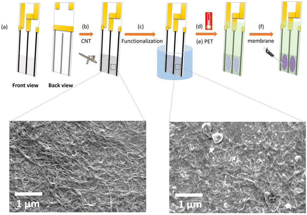 | ||
| Fig. 1 Sensor fabrication process. (a) Front and back views of three screen-printed contacts and copper tape connections, (b) air brushing CNT on the frosted part of the glass slide and SEM image of the resulting CNT film, (c) functionalizing the CNT film with 0.1 M of NaOH·15-crown-5 ether solution and SEM image of the resulting n-doped CNT film, (d) curing the sensor at 85 °C, (e) applying pre-cut clear PET sheet to cover the contacts and have specific openings, (f) drop-casting ISM solution into the openings and drying for 12 hours. | ||
2.3. Sensor testing
For each experiment, a batch of four sensors (includes three Pb2+ sensors and one blank as a control) were fabricated and tested for 3 cycles. Following the 24 hours conditioning period in 3 mg L−1 Pb(NO3)2, the sensors were connected to the eDAQ channels in ‘biosensor’ mode, which applies a constant 10 mV across the sensor and records current changes over time (2000 nA range) at 30 data points per minute. They were then lowered into a 1 L solution of 200 mg L−1 tris-acetate buffer solution at pH 5.5 (background solution). Prior to spiking the various concentrations of Pb2+, the sensors were left to stabilize in the stirred background solution, then the solution was spiked with Pb2+ ions, added from 50 mg L−1 and 500 mg L−1 solutions of Pb(NO3)2 as stock solutions. The current was normalized relative to the baseline current, I0, calculated by averaging the last 30 measurements (60 s), represented as % response (eqn (1)). | (1) |
3. Results and discussion
3.1. Optimizing the sensor fabrication for sensitivity
Single-walled carbon nanotubes (SWCNTs) were chosen for the resistive film in the Pb2+-selective chemiresistors since they combine high electrical conductivity with high surface area and chemical stability.35 For comparison, a batch of sensors including a bare sensor (resistive film: SWCNTs) and three Pb2+ sensors (SWCNTs coated with ISM) were fabricated with a previously reported method using copper tape after air-brushing the CNT film and with a circular opening for the ISM.31 The bare air-brushed CNT films did not show a clear response to Pb2+ ions, only a slight decrease in current was observed at higher concentrations whereas the response of the films covered with ISM was clearly notable at 33 μg L−1 Pb2+ (Fig. S1†). Although Pb2+ detection using ISM-covered CNT-based chemiresistors is a feasible proposition in analogy to previous work with nitrogen species,31 it does not yet fulfill the requirement of detecting less than 10 μg L−1 of analyte. A sensor with a resistive film of SWCNTs functionalized with NaOH·15-crown-5 ether solution34 (f-SWCNTs) was able to detect as little as 10 μg L−1 Pb2+ (Fig. S2†) with a maximum average response of 4.3% at 3.3 mg L−1 Pb2+. The hydroxide ions are oxidized by the CNTs to form hydrogen peroxide. The reduced nanotubes are negatively charged with n-type behaviour. This negative charge and the presence of oxygen defects on the CNT film facilitate interactions with the cationic crown ether complex, increasing the stability of the percolation network. Hence, the NaOH·15-crown-5 ether mixture not only n-dopes the CNT film, but also protects the resistive film by forming a highly stable Na+-crown ether complex.34,36 As a result, the baseline of the sensor becomes less noisy, so the relative standard deviation (RSD) is reduced, the signal-to-noise (S/N) ratio and also the sensitivity improve (Fig. 2a). Comparing the baseline of the non-functionalized and functionalized resistive films, the S/N ratio increased from 1340 to 1750 and the RSD decreased by 0.19% from 0.76% after functionalization (Fig. 2a). The calculated LoD for the Pb2+ sensor with the f-SWCNT film decreased to 10 μg L−1.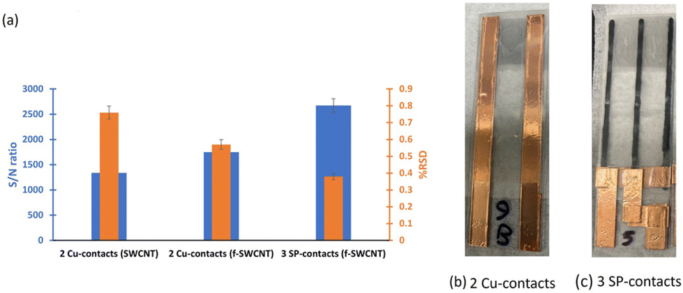 | ||
| Fig. 2 Lead(II) sensor modification by functionalization of the resistive film and improving the sensor fabrication. (a) Signal-to-noise ratio (blue bars) and %RSD (orange bars) values of various lead(II) sensors: 1. made of air-brushed SWCNT film coated with ISM and two copper contacts, 2. made of air-brushed f-SWCNT film coated with ISM and three screen-printed (SP) carbon contacts, (b) image of an actual lead(II) sensor with two copper contacts geometry, (c) image of an actual lead(II) sensor with three screen-printed (SP) carbon contacts geometry. | ||
To lower the LoD even further below 10 μg L−1, the sensor geometry was changed to improve contact stability and expose a larger fraction of the resistive film to the ISM. The copper tape contacts were replaced with screen printed carbon contacts, and the aspect ratio of the resistive film was changed using a 3-contact geometry with two narrower channels to enable higher measurement currents at constant film thickness and applied bias. As a result, the S/N ratio of the baseline dramatically increased to 2670 with a lower RSD, 0.38% on average (Fig. 2a). More importantly, the effective surface area using two oval-shape openings (7 mm × 18 mm) increased 5-fold over the old fabrication protocol with a circular window (7 mm diameter). The two types of geometries can be compared in Fig. 2b and c. Rectangular windows were not feasible due to membrane detachment in the corners. Since the surface area of the air-brushed CNT film is the same, by this strategy, 55.0% of the CNT film was exposed to the ISM instead of 20.8%. Optimization of fabrication and sensor geometry resulted in detection as low as 3.3 μg L−1.
3.2. Lead(II) sensor performance
The selected ionophore for this study, lead ionophore IV (tert-butylcalix[4]arene-tetrakis(N,N-dimethylthioacetamide)), is the most sensitive commercially available ionophore for lead (Fig. 3a).33,37–39 A solid-contact ISE made of this ionophore with the same applied membrane composition was reported to operate above 200 μg L−1,40 well above the MAC in drinking water. Even though several improvements to this LoD were reported such as using different conditioning, measuring protocols and membrane composition,41 utilizing thin layer technology for applying the ISM,42 and transduction and amplification of potentiometric signals,43 a reference electrode was nevertheless required in all cases.19,44–49 Hence, the fabrication of a highly sensitive chemiresistive device for Pb2+ detection is a significant achievement, for its simplicity and independence from a reference electrode. First, the performance of the optimized Pb2+ sensor was compared to bare and blank sensors. The Pb2+ sensor operated selectively and sensitively compared to the bare (f-SWCNT film without the membrane) and the blank (f-SWCNT film coated with a membrane missing the ionophore in its composition). The bare and blank devices did not respond to 10 μg L−1 Pb2+ and responded less than 0.7% to 100 μg L−1 Pb2+ while the ion-selective chemiresistive sensor showed a clear response at 10 μg L−1 (more than 1%) and 3.0% response to 100 μg L−1 Pb2+ (Fig. 3b).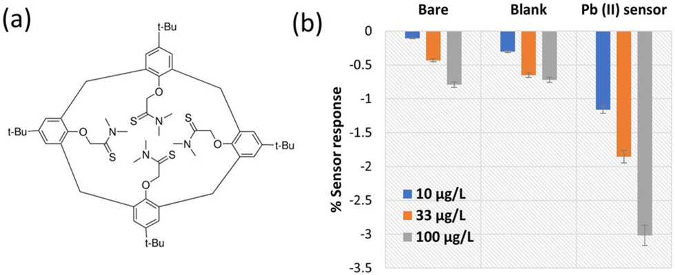 | ||
| Fig. 3 (a) Structure of lead ionophore IV, tert-butylcalix[4]arene-tetrakis(N,N-dimethylthioacetamide), (b) percent sensor response of bare (resistive film: f-SWCNT), blank (resistive film: f-SWCNT coated with blank membrane without ionophore) and Pb2+ sensors (resistive film: f-SWCNT coated with ISM) to 10 μg L−1 (blue bars), 33 μg L−1 (orange bars) and 100 μg L−1 (gray bars) of Pb2+ in 200 mg L−1 tris-acetate buffer solution at pH 5.5. | ||
The clear step-down response of a typical fabricated Pb2+ sensor in a concentration range of 3.3 to 3300 μg L−1 is shown in Fig. 4a. Sensors were immersed in 200 mg L−1 tris-acetate buffer solution at pH 5.5. The pH 5.5 was chosen as the optimized pH after studying the effect of pH on the sensor response since the sensor at this pH showed slightly higher response than other pHs (Fig. S3†). Owing to the properties of the used ionophore, it can be protonated in low pHs and lose its function in complex formation with Pb2+. Also, at pHs higher than 6.5, the formation of Pb(OH)+ or/and Pb(OH)2 can decrease the concentration of Pb2+ ions in the solution.33,40,50,51 A representative calibration curve was obtained from averaged data of three cycles of the same sensor (Fig. S4†) and error bars were defined as ±standard deviation of three data points at each concentration (Fig. 4b). The sensor responses were fitted with a Langmuir-style equation (eqn (2)).52 Due to the deviation from the fit at high concentrations, a calibration curve for the lower concentrations is shown in the inset of Fig. 2b. The LoD of the sensor was calculated as 1.75 μg L−1. The linearized Langmuir adsorption model, 1/(% − sensor response) vs. 1/[Pb2+] is plotted and shown in Fig. 4c.
 | (2) |
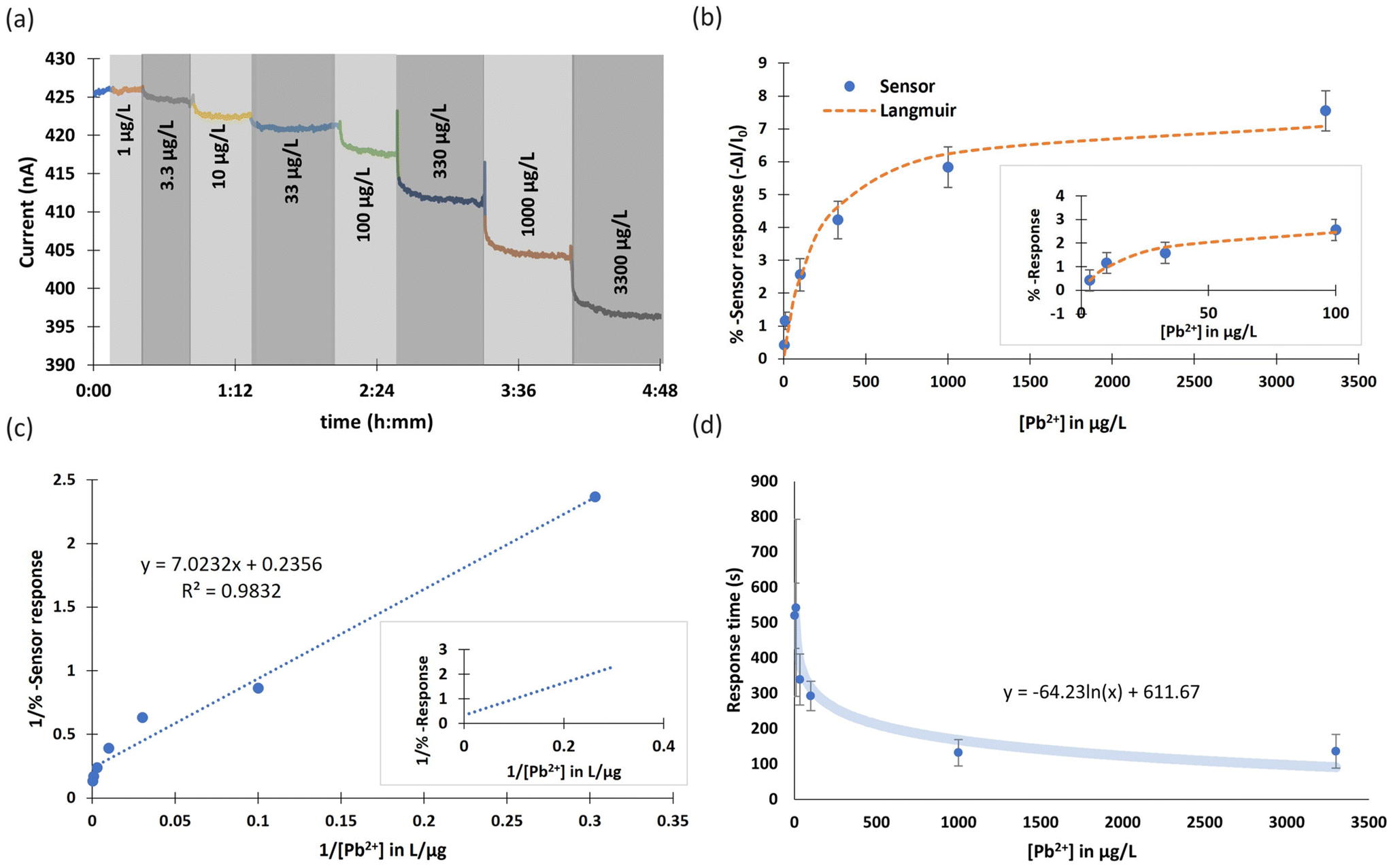 | ||
| Fig. 4 (a) Pb2+-selective chemiresistive sensor response to Pb2+ over time in 200 mg L−1 tris-acetate buffer solution at pH 5.5, (b) Calibration curve of the sensor response vs. the concentration of Pb2+ (in a concentration range of 3.3–3300 μg L−1) fitted with a Langmuir equation (fitting parameters, A and B are 7.53% and 0.0048 L μg−1 respectively), inset: calibration curve of the sensor in the lower range only (3.3–100 μg L−1) with fitting parameters, A and B, 2.96% and 0.049 L μg−1 respectively, (c) linearized calibration curve of the fabricated sensor vs. the concentration of Pb2+ (in a concentration range of 3.3–3300 μg L−1), inset: zoomed-in linearized calibration curve of the sensor in lower concentrations (3.3–100 μg L−1), (d) Average response time as a function of Pb2+ concentration in a range of 3.3–3300 μg L−1. | ||
The sensors responded more slowly to lower concentrations (Fig. 4d). The average response time for 95% of the response at 3.3 μg L−1 (the lowest measured detectable concentration) was 8.6 min whereas the average response time at 3300 μg L−1 (the highest concentration) was 2.3 minutes, with an approximately logarithmic relationship (Fig. 4d). The sensor baseline drift over three cycles was on average 1.75 pA s−1. The RSD as a measure of reproducibility was calculated as 14.5% for an individual sensor. Since each sensor in this study is fabricated by hand, responses from different devices cannot be meaningfully averaged. In case of the device geometry used in this study, the best sensor performance in terms of sensitivity and response time was found for a resistance of the deposited CNT film of about 9 kΩ. For optimizing the resistance of the resistive film, three batches of sensors were fabricated (with different range of resistances) the results of which are compared in Table S1.† Resistive films with a resistance of about 9 kΩ were more sensitive with lower LoD and faster response to Pb2+ ions. The electrical resistance of CNT film is a more accurate representation than “thickness” or “density” of the loosely packed percolation network that forms the film. “Thicker” deposited CNT films (i.e. lower resistances) have slower response times and lower sensitivity while higher resistance (thinner) films demonstrated a little faster response since charge transfer is easier across the film but compared with the optimized resistance (9 kΩ) showed smaller responses with higher LoD. The uniformity of the CNT films in different resistance ranges were investigated by SEM at lower magnifications. The images with 100× magnification show 1 × 1 mm2 of the chip, which is 1/100 of the whole surface area of the chip. Overall, the uniformities of the air-brushed CNT films are quite high for all three batches, specifically batch no. 1 and 2 (Fig. S5†). Responses of the other sensors in the same range of resistance of batch 1 are shown in Fig. S6,† which also confirms that each of these sensors is reproducible and reusable.
Due to the properties of ISMs, the Pb2+ sensors in this study operated reversibly albeit with slow recovery (Fig. S7†). For the recovery test, the sensors were immersed in a background solution (200 mg L−1 tris/acetate buffer). The sensor averaged a 111.9% recovery after 170 minutes when placed into a lead-free tris-acetate solution at pH 5.5 with an average response of 7.3% (individual cycles: 7.3%, 7.6%, 6.9%) and an average recovery of 8.2% (individual cycles: 7.3%, 8.4%, 8.9%) over three cycles. This slow recovery is likely due to the strong bonding between Pb2+ ions and C![[double bond, length as m-dash]](https://www.rsc.org/images/entities/char_e001.gif) S groups in the ionophore. Remarkably, none of the published reports of Pb2+ sensors using this ionophore mention a recovery time even though all of them claim that the sensors are reusable with high reproducibility.19,40,44,46–49 While the fabricated Pb2+ chemiresistive sensor can be reset and reused, this may not be desirable in all application scenarios once lead contamination has been established.
S groups in the ionophore. Remarkably, none of the published reports of Pb2+ sensors using this ionophore mention a recovery time even though all of them claim that the sensors are reusable with high reproducibility.19,40,44,46–49 While the fabricated Pb2+ chemiresistive sensor can be reset and reused, this may not be desirable in all application scenarios once lead contamination has been established.
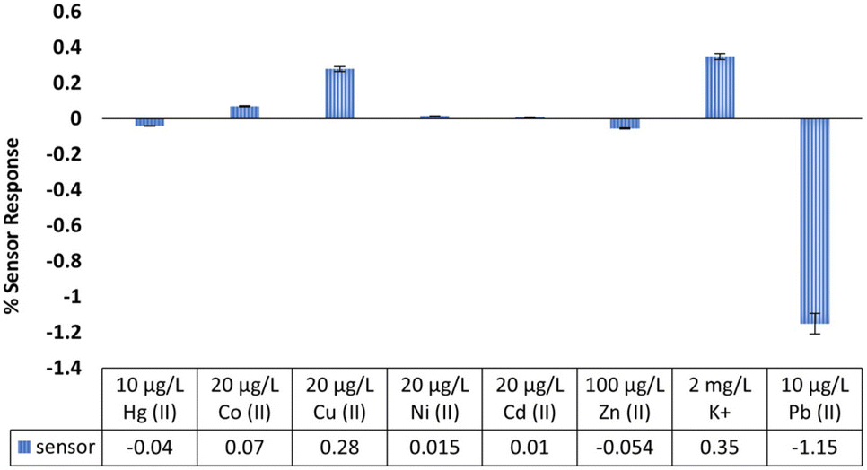
A batch of three sensors were tested in the presence of different interfering ions to determine the feasibility for use in drinking water samples. The tested concentrations of heavy metals and potassium were higher than their common concentrations in drinking water:53 Hg2+ (10 μg L−1), Co2+ (20 μg L−1), Cu2+ (20 μg L−1), Ni2+ (20 μg L−1), Cd2+ (20 μg L−1), Zn2+ (100 μg L−1), K+ (2 mg L−1), Pb2+ (10 μg L−1). Each interferant was added into the background solution in the given order and the sensor response to 10 μg L−1 Pb2+ was tested at the end. No significant interference was observed (Fig. 5) and the data is consistent with literature reports on potentiometric applications of this ionophore.40 The sensor response to 10 μg L−1 Pb2+ (−1.15%) in the presence of other heavy metals and 2 mg L−1 K+ was also comparable with its response in the absence of these ions (1.16%), confirming that small changes in conductivity do not impact the sensor response to Pb2+.
 | ||
| Fig. 5 Selectivity test of the fabricated Pb2+ sensor in 200 mg L−1 tris-acetate buffer solution at pH 5.5. Response of the Pb2+ sensor to 10 μg L−1 Pb2+ in the presence of interfering ions at common concentrations in drinking water. | ||
3.3. Real sample test
City of Hamilton tap water54 (pH = 7.45, conductivity 0.29 mS cm−1) was collected and filtered through a 0.2 μm Waltman filter paper, pH-adjusted to 5.5 with acetic acid, and stored at 4 °C when not in use. No further sample treatment was done. Several standard solutions of Pb2+ ions (3.3, 10, 33, 100 and 330 μg L−1) were prepared in tap water. Two sensors were used to measure 10 μg L−1 Pb2+ (to ensure repeatability) and one sensor was tested with 33 μg L−1 Pb2+. The sensors were immersed in the tap water (0 μg L−1 Pb2+) overnight and the current was recorded to ensure the sensors were working properly with stable baselines. All sensors were titrated three times to prepare their calibration curves (Fig. S8a–c†). Subsequently, the sensors were kept in tap water for 4 hours until a stable baseline was achieved. Two sensors were then immersed in solutions spiked with 10 μg L−1 Pb2+ and one sensor was immersed in 33 μg L−1, the solutions were then replaced with blank solutions. The sensor responses were recorded continuously in each case while the jar switching was repeated three times (Fig. S8d–f†) and the average response of each sensor reported in Table 1. By comparing the results between the spiked concentrations and found concentrations of each sensor, the average recovery was calculated to be 98.7% with acceptable ranges of error. These Pb2+ sensors are therefore promising to be utilized for real world sample analysis. Reagent-free operation can be achieved in combination with water electrolysis to locally acidify the water and avoid formation of Pb(OH)+ and Pb(OH)2.| Added analyte (μg L−1) | Found by sensor (μg L−1) | Recovery (%) |
|---|---|---|
| 0 | <3.3 | — |
| 10 | 9.78 ± 0.62 | 97.98 ± 6.21 |
| 10 | 10.38 ± 0.96 | 103.86 ± 9.64 |
| 33 | 31.10 ± 0.55 | 94.24 ± 1.66 |
3.6. Sensing mechanism
A discussion of the sensing mechanism for this sensor needs to consider each step of the fabrication, comparing the responses with and without membrane, as well as of pristine or modified CNT films. Hall measurements (Table S2† and Fig. 6) and Raman spectroscopy (Fig. S9†) are also performed to elucidate the behaviour of the resistive film at each step.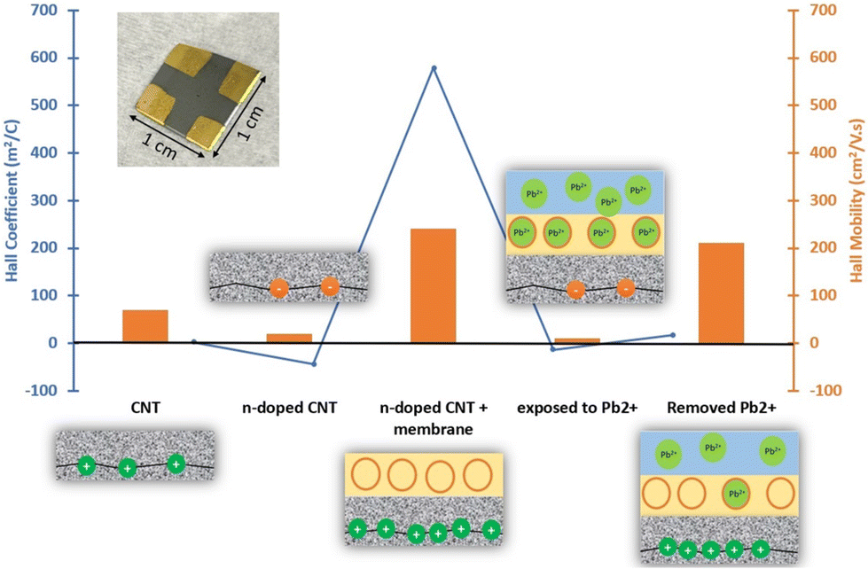 | ||
| Fig. 6 Hall coefficients and Hall mobilities after each fabrication step, Pb2+ exposure and recovery, accompanied by a schematic of the resistive film at each step. Inset: Image of the fabricated four-probe device for Hall measurements. | ||
Exposing a bare device made of pristine SWCNTs to high concentrations of Pb2+ (>100 μg L−1), a slight decrease in current was observed since the pristine CNT network is slightly p-doped. When Pb2+ ions are captured by ionophores in the membrane of an ISM-covered pristine CNT network, the membrane is getting positively charged and acts as a positive electric field gating the p-doped CNT channel, resulting in a drop in current.24 After addition of the Pb(II) ISM, the same trend was observed but with a higher percentage response at lower concentrations (33 μg L−1) compared to the bare and the blank. Hence, the sensor is working based on the same principle with better sensitivity since the membrane preconcentrates the analyte and passes it through to the resistive film (Fig. S1†).
The sensor response was expected to invert after modification with the NaOH·15-crown-5 ether mixture due to having a n-type channel being gated by the positive electric field formed by Pb2+ ions, resulting in an increase in current. In our devices, however, the same current decrease was observed as the sensor response. This requires a closer look at the different steps of the fabrication process.
By doing Hall measurement on the device, the sheet resistivity, sheet Hall resistance coefficient, Hall mobility and charge carrier density data were recorded at each step of fabrication (Table S2† and Fig. 6). The Hall coefficient represents the type of the semiconducting (resistive) film, negative values mean it is n-type and positive values show it is p-type. Initially, Hall measurement data confirmed that pristine CNTs were slightly p-doped. After modification with NaOH·15-crown-5 ether mixture the film became slightly n-doped (Table S2† and Fig. 6 and 7a), in agreement with previous reports.55 Data also revealed that the addition of the ISM on top of the resistive film made it highly p-doped. This may be due to an electron-withdrawing effect of the thioamide group in the ionophores on the n-doped CNT film.32,56,57 This interaction between the ionophores and the CNT film is so strong that it can change the dominant charge carriers in the film and make the film p-doped again (Fig. 7b).
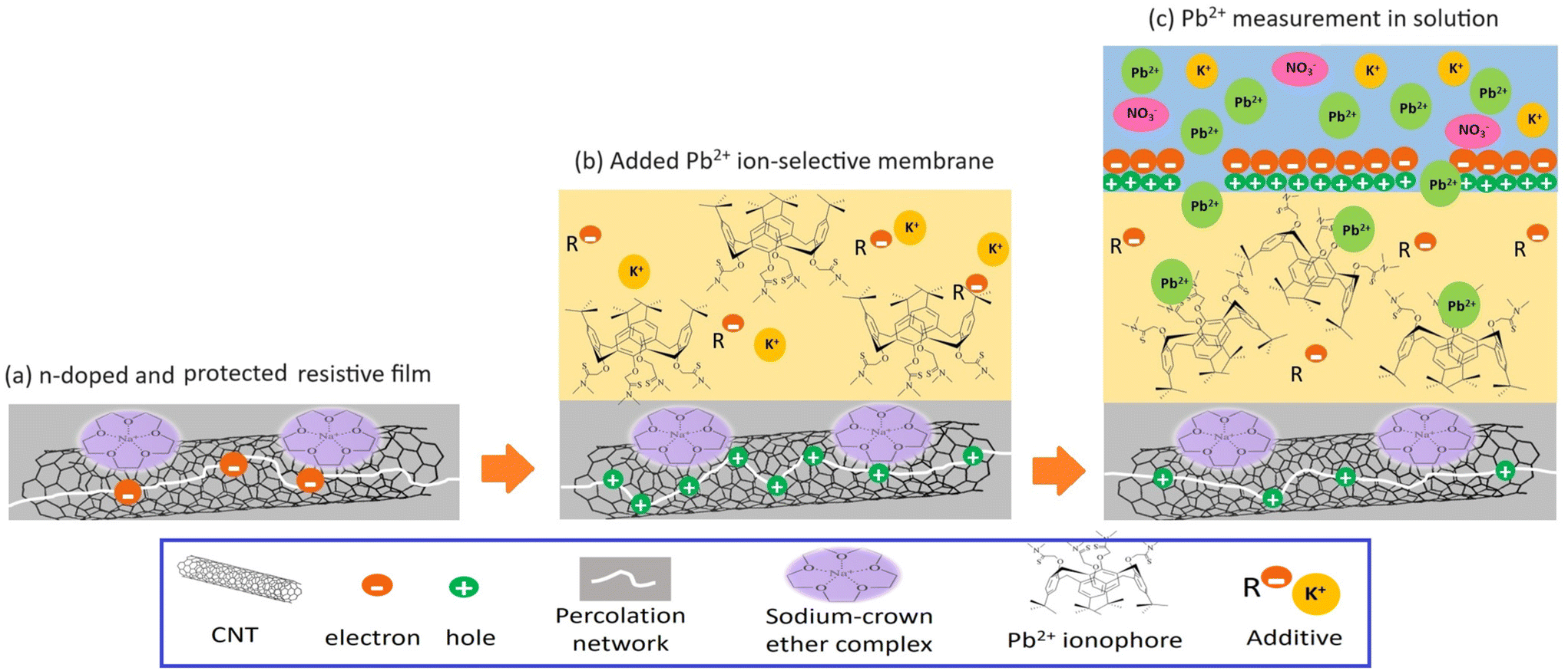 | ||
| Fig. 7 Sensing mechanism of a Pb2+ ion-selective chemiresistive sensor. (a) Cross-sectional view of the slightly n-doped f-SWCNT resistive film, (b) coated with ISM which turned it p-doped and (c) immersed in the background solution and exposed to Pb2+ ions which decreased the number of holes. | ||
According to the Hall measurement data (Table S2† and Fig. 6), the fabricated and ready-to-use sensor initially has a p-doped resistive film. After conditioning the sensor in 3 mg L−1 Pb2+ solution for 24 hours, the Hall coefficient of the device became negative due to the high affinity of the ionophore towards Pb2+ ions causing a loss of ionophore–CNT interactions. The complexation is aided by the strong affinity of the thioamide groups for Pb2+ and the good fit of the calix[4]arene cavity to the size of Pb2+ ions.37,38 Because the Pb2+ concentration in the conditioning solution was very high, it resulted in reverting the resistive film to n-doped whereas in Pb2+ experiments with regular fabricated Pb2+ chemiresistive sensors on glass slides in a concentration range of 3.3–3300 μg L−1 Pb2+ the number of holes of the p-type resistive film gets merely reduced upon interaction with the analyte and a decrease in current is observed as the sensor response (Fig. 7c).
The fabricated devices for Hall measurements were left in DI water for 5 hours to remove the Pb2+ ions from the device. As it can be seen in Fig. 6, “removed Pb2+” step, the Hall coefficient of resistive film returned to positive values as a reverse process. Overall, during the sensor fabrication, measurement and recovery process, the doping type of the CNT film was changed multiple times. Of note, the Hall mobility of the negative charge carriers is always very low, meaning that the resistance of n-doped films is higher whereas p-doped devices exhibit high Hall mobility values (Table S2† and Fig. 6).
Raman spectroscopy was used to investigate the interactions of the CNT film in more details, although Raman data could not be obtained from ISM-coated films (Fig. S9†). Raman spectra taken from pristine and n-doped CNT films confirm that the 2D band is slightly down-shifted from 2595.5 cm−1 to 2592.9 cm−1 which is a sign of mild n-doping even though the defect density of the surface has not changed with similar ID/IG peak intensity ratios (0.13 to 0.12) (Fig. S9†).58 When the n-doped CNT film was exposed to 3 mg L−1 Pb2+ for 5 hours, it got p-doped and the 2D band up-shifted (from 2592.9 cm−1 to 2596.4 cm−1). The CNT percolation network became more disordered as seen by the change in the ID/IG ratio from 0.12 to 0.17 (Fig. S9†). Indeed, Pb2+ ions tend to accept electrons from the surface. Hence, the number of negative charge carriers of the surface decreases and the number of positive charge carriers increases. We can therefore conclude from the Raman data of the CNT film that n-doping of the CNTs does not change the stability of the CNT film while Pb2+ ions interact with the CNT network, p-dope the surface and increase the defect density in agreement with sensor responses and Hall measurement results.
4. Conclusion
We successfully addressed the challenge of improving the LoD of chemiresistive Pb2+ sensors to render them suitable for online monitoring at or below regulatory limits. The CNT structure allows for easy tuning of their electrical properties. Optimizing the network by altering the mobile charge carriers and sensor geometry have a large impact on the sensor performance. We built a highly sensitive ion-selective chemiresistive sensor for Pb2+ detection by increasing the effective surface area and stability of the resistive film to increase the S/N ratio and facilitate the interaction with Pb2+. This sensor can detect between 3.3 μg L−1 and 3300 μg L−1 Pb2+ ions in aqueous solutions with an LoD of 1.75 μg L−1 which is well below current regulatory limits for lead in drinking water. The detection mechanism is based on the interaction of the ionophores in the ISM with the CNT network in the absence of Pb2+ ions. Upon being exposed to Pb2+ ions, the ionophores preferentially interact with Pb2+ ions, resulting in a decrease in current. This sensor can find applications in the drinking water distribution system, in point-of-use water filters, and in water fountains. It is sensitive, selective, and stable as well as simple to fabricate, easy to operate, robust, and cost effective. More work needs to be done to improve the fabrication process and response time, as well as verifying device stability over months and maybe even years for deployment at a large scale. The sensitivity enhancement due to ionophore interactions with the CNT film points the way towards the development of highly sensitive chemiresistors for aqueous ion detection that surpass the capabilities of potentiometric devices. Compared to potentiometric Pb2+ sensors, the proposed chemiresistive Pb2+ sensor is a first proof-of-concept and still needs to be developed further by incorporating recent advances in electrical sensors and ion-selective membranes to further enhance its sensitivity, durability, and reproducibility.Author contributions
All authors participated in manuscript review and editing. Maryam Darestani-Farahani contributed to conceptualization, did investigation and formal analysis and wrote the original draft. Isabella Mendoza Montealegre, Mehraneh Tavakkoli Gilavan and Thomas Kirby contributed to investigation. Ravi Selvaganapathy contributed to methodology. Peter Kruse administered the project, acquired funding, and contributed to conceptualization and methodology.Conflicts of interest
There are no conflicts to declare.Acknowledgements
We appreciate fruitful discussions with Johnson Dalmieda, Jonah Halili, Mae Masters, Fanqing Ma and Dr David Emslie. We thank the Adronov group for access to the Raman spectrometer. Electron microscopy was performed at the Canadian Centre for Electron Microscopy (CCEM, also supported by the Natural Sciences and Engineering Research Council of Canada (NSERC) and other government agencies).References
- E. Doré, D. A. Lytle, L. Wasserstrom, J. Swertfeger and S. Triantafyllidou, Crit. Rev. Environ. Sci. Technol., 2021, 51, 2357–2388 CrossRef PubMed.
- WHO, Guidelines for drinking-water quality, 2022, vol. 33 Search PubMed.
- L. W. Wasserstrom, S. A. Miller, S. Triantafyllidou, M. K. Desantis and M. R. Schock, J. - Am. Water Works Assoc., 2017, 109, E464–E478 CrossRef PubMed.
- J. Jency Feminus and P. N. Deepa, J. Mater. Sci.: Mater. Electron., 2019, 30, 15553–15562 CrossRef CAS.
- J. Dalmieda and P. Kruse, Sensors, 2019, 19, 5134 CrossRef CAS PubMed.
- J. Liu and Y. Lu, J. Am. Chem. Soc., 2003, 125, 6642–6643 CrossRef CAS PubMed.
- A. Shah, A. Zahid, A. Khan, F. J. Iftikhar, J. Nisar, C. Fernandez, M. S. Akhter, A. A. Almutawah and H.-B. Kraatz, J. Electrochem. Soc., 2019, 166, B3136–B3142 CrossRef CAS.
- W. Kang, X. Pei, C. A. Rusinek, A. Bange, E. N. Haynes, W. R. Heineman and I. Papautsky, Anal. Chem., 2017, 89, 3345–3352 CrossRef CAS PubMed.
- D. Zhao, X. Guo, T. Wang, N. Alvarez, V. N. Shanov and W. R. Heineman, Electroanalysis, 2014, 26, 488–496 CrossRef CAS.
- MQuant, Colorimetric Lead Test Strips, https://www.sigmaaldrich.com/CA/en/product/mm/110077, (accessed 10 October 2023).
- Spectroquant, Photometric Lead test, https://www.sigmaaldrich.com/CA/en/product/mm/109717, (accessed 10 October 2023).
- Thermo ScientificTM, OrionTM Lead Electrodes, https://www.thermofisher.com/order/catalog/product/9682BNWP, (accessed 10 October 2023).
- Mettler Toledo, DX407-Pb Lead half-cell, https://www.mt.com/us/en/home/products/Laboratory_Analytics_Browse/Product_Family_Browse_titrators_main/Product_Family_Titration_Sensors/Titration_Ion_Selective_sensors_Fami/DX407_Lead_Half_Cell.html, (accessed 10 October 2023).
- S. A. Jaywant and K. Mahmood Arif, Sensors, 2019, 19, 4781 CrossRef CAS PubMed.
- X. Du, M. Huang, R. Wang, J. Zhai and X. Xie, Chem. Commun., 2019, 55, 1774–1777 RSC.
- S. Ghosh, K. Dissanayake, S. Asokan, T. Sun, B. M. A. Rahman and K. T. V. Grattan, Sens. Actuators, B, 2022, 364, 131818 CrossRef CAS.
- J. Dalmieda, A. Zubiarrain-Laserna, D. Ganepola, P. R. Selvaganapathy and P. Kruse, Sens. Actuators, B, 2021, 328, 129023 CrossRef CAS.
- B. Molinero-Abad, D. Izquierdo, L. Pérez, I. Escudero and M. J. Arcos-Martínez, Talanta, 2018, 182, 549–557 CrossRef CAS PubMed.
- S. Yu, F. Li, T. Yin, Y. Liu, D. Pan and W. Qin, Anal. Chim. Acta, 2011, 702, 195–198 CrossRef CAS PubMed.
- D. W. Kimmel, G. Leblanc, M. E. Meschievitz and D. E. Cliffel, Anal. Chem., 2012, 84, 685–707 CrossRef CAS PubMed.
- P. W. Sayyad, N. N. Ingle, T. Al-Gahouari, M. M. Mahadik, G. A. Bodkhe, S. M. Shirsat and M. D. Shirsat, Chem. Phys. Lett., 2020, 761, 138056 CrossRef CAS.
- A. Maity, X. Sui, C. R. Tarman, H. Pu, J. Chang, G. Zhou, R. Ren, S. Mao and J. Chen, ACS Sens., 2017, 2, 1653–1661 CrossRef CAS PubMed.
- C. Wang, X. Cui, Y. Li, H. Li, L. Huang, J. Bi, J. Luo, L. Q. Ma, W. Zhou, Y. Cao, B. Wang and F. Miao, Sci. Rep., 2016, 6, 1–8 CrossRef PubMed.
- G. Zhou, J. Chang, S. Cui, H. Pu, Z. Wen and J. Chen, ACS Appl. Mater. Interfaces, 2014, 6, 19235–19241 CrossRef CAS PubMed.
- T. Pham, Y. Chen, J. Lopez, M. Yang, T. T. Tran and A. Mulchandani, Biosensors, 2021, 11, 1–13 Search PubMed.
- A. Zubiarrain-laserna and P. Kruse, J. Electrochem. Soc., 2020, 167, 037539 CrossRef CAS.
- M. Ehsani, P. Rahimi and Y. Joseph, Sensors, 2021, 21, 3291 CrossRef CAS PubMed.
- M. Deb, S. Saxena, R. Bandyopadhyaya and S. Shukla, Mater. Sci. Eng., B, 2021, 272, 115323 CrossRef CAS.
- P. Kruse, J. Phys. D: Appl. Phys., 2018, 51, 203002 CrossRef.
- J. Dalmieda, A. Zubiarrain-Laserna, D. Saha, P. R. Selvaganapathy and P. Kruse, J. Phys. Chem. C, 2021, 125, 21112–21123 CrossRef CAS.
- M. Darestani-farahani, F. Ma, V. Patel, P. R. Selvaganapathy and P. Kruse, Analyst, 2023, 148, 5731–5744 RSC.
- E. Hoque, T. Chowdhury and P. Kruse, Surf. Sci., 2018, 676, 61–70 CrossRef CAS.
- E. Malinowska, Z. Brzózka, K. Kasiura, R. J. M. Egberink and D. N. Reinhoudt, Anal. Chim. Acta, 1994, 298, 253–258 CrossRef CAS.
- Y. Nonoguchi, M. Nakano, T. Murayama, H. Hagino, S. Hama, K. Miyazaki, R. Matsubara, M. Nakamura and T. Kawai, Adv. Funct. Mater., 2016, 26, 3021–3028 CrossRef CAS.
- G. Cho, S. Azzouzi, G. Zucchi and B. Lebental, Sensors, 2022, 22, 218 CrossRef CAS PubMed.
- Y. Iihara, T. Kawai and Y. Nonoguchi, Chem. – Asian J., 2020, 15, 590–593 CrossRef CAS PubMed.
- J. Kulesza and M. Bochenska, Eur. J. Inorg. Chem., 2011, 6, 777–783 CrossRef.
- M. Guziński, G. Lisak, J. Kupis, A. Jasiński and M. Bocheńska, Anal. Chim. Acta, 2013, 791, 1–12 CrossRef PubMed.
- A. Ceresa and E. Pretsch, Anal. Chim. Acta, 1999, 395, 41–52 CrossRef CAS.
- H. A. Arida, A. Al-Haddad and M. J. Schöning, WIT Trans. Modell. Simul., 2011, 51, 547–557 Search PubMed.
- A. Ceresa, E. Bakker, B. Hattendorf, D. Günther and E. Pretsch, Anal. Chem., 2001, 73, 343–351 CrossRef CAS PubMed.
- E. Zdrachek and E. Bakker, Electroanalysis, 2021, 33, 1225–1232 CrossRef CAS.
- J. Zhai, D. Yuan and X. Xie, Sens. Diagn., 2022, 1, 213–221 RSC.
- M. Püntener, T. Vigassy, E. Baier, A. Ceresa and E. Pretsch, Anal. Chim. Acta, 2004, 503, 187–194 CrossRef.
- R. J. W. Lugtenberg, R. J. M. Egberink, A. Van Den Berg, J. F. J. Engbersen and D. N. Reinhoudt, J. Electroanal. Chem., 1998, 452, 69–86 CrossRef CAS.
- C. Liu, X. Jiang, Y. Zhao, W. Jiang, Z. Zhang and L. Yu, Electrochim. Acta, 2017, 231, 53–60 CrossRef CAS.
- S. Alva, A. Widinugroho, M. Adrian, D. S. Khaerudini, S. E. Pratiwi and A. S. A. Aziz, J. Electrochem. Soc., 2019, 166, B1513–B1519 CrossRef CAS.
- J. Sutter, E. Lindner, R. E. Gyurcsányi and E. Pretsch, Anal. Bioanal. Chem., 2004, 380, 7–14 CrossRef CAS PubMed.
- T. Yin, D. Pan and W. Qin, J. Solid State Electrochem., 2012, 16, 499–504 CrossRef CAS.
- Á. Golcs, V. Horváth, P. Huszthy and T. Tóth, Sensors, 2018, 18, 1407 CrossRef PubMed.
- X. Yang, N. Kumar, H. Chi, D. B. Hibbert and P. W. Alexander, Electroanalysis, 1997, 9, 549–553 CrossRef CAS.
- A. Zubiarrain-Laserna, S. Angizi, M. A. Akbar, R. Divigalpitiya, P. R. Selvaganapathy and P. Kruse, RSC Adv., 2022, 12, 2485–2496 RSC.
- Government of Ontario, Provincial Water Quality Monitoring Network Website, https://www.ontario.ca/environment-and-energy%0A/map-provincial-stream-water-quality-monitoring-network, (accessed 19 January 2023).
- Drinking Water Systems Annual Water Quality and Summary Report, https://www.hamilton.ca/home-neighbourhood/water-wastewater-stormwater/water-treatment-distribution/drinking-water-0, (accessed 21 October 2023).
- Y. Nonoguchi, A. Tani, T. Ikeda, C. Goto, N. Tanifuji, R. M. Uda and T. Kawai, Small, 2017, 13, 1–5 CrossRef PubMed.
- K. R. Moonoosawmy and P. Kruse, J. Phys. Chem. C, 2009, 113, 5133–5140 CrossRef CAS.
- D. W. M. Arrigan, G. Svehla, S. J. Harris and M. A. McKervey, Electroanalysis, 1994, 6, 97–106 CrossRef CAS.
- R. Dover, C. Klein, V. Gutkin, J. Zessin, V. Saik, D. Rotem, O. Millo, D. Porath and G. Sarusi, ACS Appl. Nano Mater., 2021, 4, 13279–13287 CrossRef CAS.
Footnote |
| † Electronic supplementary information (ESI) available. See DOI: https://doi.org/10.1039/d4an00159a |
| This journal is © The Royal Society of Chemistry 2024 |