
Noble metal-free SERS: mechanisms and applications
Sila
Jin†
ab,
Daxin
Zhang†
c,
Bo
Yang
*d,
Shuang
Guo
e,
Lei
Chen
f and
Young Mee
Jung
 *ae
*ae
aKangwon Radiation Convergence Research Support Center, Kangwon National University, Chuncheon 24341, Korea. E-mail: ymjung@kangwon.ac.kr
bDepartment of Chemistry, University at Albany, State University of New York, Albany, New York 12222, USA
cCollege of Science, Jilin Institute of Chemical Technology, Jilin, 132022, China
dSchool of Pharmaceutical Sciences, Changchun University of Chinese Medicine, Changchun 130117, P.R. China. E-mail: yangbo0623@126.com
eDepartment of Chemistry, Institute for Molecular Science and Fusion Technology, Kangwon National University, Chuncheon 24341, Korea
fSchool of Materials Science and Engineering, Jilin Jianzhu University, Changchun 130118, China
First published on 1st December 2023
Abstract
Surface-enhanced Raman scattering (SERS) is a very important tool in vibrational spectroscopy. The coupling of nanomaterials induces local surface plasmon resonance (LSPR), which contributes greatly to SERS. Due to its remarkable sensitivity in trace detection, SERS has gained prominence in the fields of catalysis, biosensors, drug tracking, and optoelectronic devices. SERS activity is believed to be closely related to the LSPR and charge transfer (CT) of the material. Noble metal nanostructures have been commonly used as SERS-active substrates due to their strong local electric fields and relatively mature preparation, application, and enhancement mechanisms. In recent years, SERS research based on semiconductor materials has attracted significant attention because semiconductor materials have advantages such as repeatable preparation, simple pretreatment, stable SERS spectra and superior biocompatibility, stability, and reproducibility. Semiconductor-based SERS has the potential to enrich SERS theory and applications. Thus, the development of semiconductor materials will introduce a new epoch for SERS-based research. In this review, we outline the two main kinds of semiconductor SERS-active substrates: inorganic and organic semiconductor SERS-active substrates. We also provide an overview of the SERS mechanism for different kinds of materials and SERS-based applications.
1. Introduction
1.1 Surface-enhanced Raman scattering (SERS) and SERS mechanism
The development of SERS has a relatively short history since Fleischmann et al. discovered a significant increase in the Raman scattering intensity of pyridine on a rough silver electrode.1 However, without considering the influence of the silver nanostructures in the electrode, they suggested that the unusual intensity of the Raman signals was due to the increased surface area of the rough substrate, resulting in an increase in the number of adsorbed pyridine molecules. Subsequently, some researchers focused on studying the generation mechanism of SERS. In 1977, Jeanmarie and Van Duyne as well as Albrecht and Creighton pointed out that the enhancement factors (EFs) of 105–106 were likely due to the effective Raman cross section.2,3 Within a few years, many kinds of molecules adsorbed on SERS-active substrates were confirmed to produce strong enhanced Raman signals. Moreover, Albrecht and Creighton proposed a resonance Raman effect associated with plasmon excitation. Subsequently, Moskovits recognized the correlation between the SERS intensity and the enhancement field generated by local surface plasmon resonance (LSPR) in nanostructured metals.4 Notably, while isolated nanostructures can provide substantial Raman scattering amplification, the greatest enhancements are usually observed within narrow gaps between nanoparticles (NPs), often referred to as “hot spots”, resulting in signal enhancements of approximately 6–7 orders of magnitude.5,6 The synergy of the extremely high sensitivity offered by plasmonic nanomaterials, the inherent structural specificity of Raman spectra, and the experimental versatility of SERS has made SERS an exceptionally powerful analytical technique.7,8 Although SERS has grown into a rich field of research and technology in the decades since its discovery, continued efforts are needed to achieve the goals of routine use in analytical and commercial products. For practical application, a SERS-active substrate should be homogeneous, reproducible, cost-effective, and easy to fabricate. However, the manufacturing cost of noble metal array structures is high, as expensive equipment and the involvement of high-tech personnel are typically necessary, and the fabrication process is complex.9 In contrast, most semiconductors, such as MXene, graphene, ZnO, and TiO2, can be fabricated relatively simply.10,11 Another reason is that high SERS intensity and substrate stability are fundamental properties of semiconductors, whereas the aggregation of noble metal nanoparticles is a dynamic process, and detection must be performed in a very short time. Lasers induce metal nanoparticle aggregation, leading to nonreproducible spectra. In addition, the temperature causes the ejection of high-energy hot carriers from the metal surface, leading to the desorption, photodecomposition, or photobleaching of probe molecules.12 In contrast, semiconductors with stable structures and properties provide reproducible SERS intensities. Most importantly, semiconductors can effectively prevent photoluminescence, which is always induced by aggregate metal nanoparticles. Thus, semiconductor-based SERS-active substrates are considered promising materials with high potential for practical applications.11,13The electromagnetic enhancement (EM) mechanism and chemical enhancement (CM) mechanism are commonly considered in studies to understand the significant enhancement of Raman signals.14–23 The EM mechanism is generally believed to dominate SERS enhancement due to the large electromagnetic field caused by the collective oscillation of surface plasmons (SPs) in metal particles. The CM mechanism stems from a short-range effect of light-induced charge transfer (CT) between molecules and metals, and charge transfer resonance (CTR) enhancement plays an important role in CM.
1.2 SERS enhancement mechanisms of semiconductor–molecular nanostructures
Most observations of semiconductor-enhanced Raman scattering involve the CT mechanism, in which electrons transfer between semiconductors and molecules of heterogeneous structures, providing a new way to explore the CM mechanism of SERS. Since the discovery in 1982 that semiconductors show SERS activity, SERS-active semiconductor materials have been greatly expanded from metal oxides and silver halides to single-element semiconductors and sulfide and arsenide semiconductors.24 Metal oxides are the most widely studied semiconductors in SERS research. Semiconductors such as zinc oxide (ZnO),25,26 titanium dioxide (TiO2),27–30 and copper oxides (CuO and Cu2O)31 are becoming popular research targets. Yamada et al. studied SERS on crystalline TiO2 (001) and NiO (110) surfaces at an early stage.24,32 The Raman scattering was enhanced due to chemical bonding between pyridine nitrogen and NiO or TiO2 atomic sites, and this molecule–semiconductor interaction was similar to the resonant Raman scattering effect.Jiang et al. devised a scheme to investigate the CT mechanism of TiO2 molecules by using 4-mercaptobenzoic acid (4-MBA) and 4-aminophenol (PATP) as probe molecules.28 Based on a TiO2 photonic microarray, the SERS sensitivity and activity can be improved through increased interaction of light by repeated and multiple light scattering.33 In addition, a SERS study on ZnO suggested that ZnO nanocrystals of 20 nm exhibit enhancement of 103 for the Raman probe 4-mercaptopyridine (4-MPY).25 ZnO has a size-related CTR in the range of 18–31 nm in diameter.26 In both cases, CM is the most likely cause of the observed Raman enhancement. In addition to metal oxides, silver halides AgX (X = Cl, Br, and I)34–36 and single-element semiconductors (graphene, Si, and Ge)37,38 have been shown to exhibit Raman enhancement effects based on the CT mechanism. In the AgCl pyridine colloid, in addition to the contribution of local field enhancement to the photolysis of Ag particles, the Ag+ complex on the surface of the AgCl colloid plays an important role in the SERS enhancement of pyridine.34 The first-layer effect of graphene-enhanced Raman scattering (GERS), which strongly depends on the distance between graphene and molecules, also proves the CM of graphene.38
Compared to metals, semiconductor materials show the advantages of more controllable band gaps, photoluminescence (PL), and stability. However, SERS studies of semiconductor nanomaterials have shown that several parameters, including the material size, surface defects, and morphology, have significant effects on semiconductor Raman scattering. The observed Raman spectral profile is completely different from that exhibited on metal substrates due to the narrow size distribution of semiconductors. The half-peak width becomes narrower with decreasing particle size, which is a quasiresonant phenomenon. The surface state energy levels formed by defect-bound electrons on the semiconductor surface provide more energy levels for the CT transition, increasing the CT contribution to SERS.23
1.3 Selection of substrates for SERS
Because SERS signal enhancement requires the presence of high-density hot spots on metal surfaces, many studies have focused on developing materials and substrates with high concentrations of hot spots. The materials used to detect various analytes include noble metal NPs, composite NPs, core–shell NPs, metal oxides, single-element semiconductors, and some nanoscale-based hybrid materials. The size, direction, shape, distance between particles, dielectric properties, and surface characteristics of the material greatly influence the observed enhancement effect.39–41Traditionally, SERS-active substrates have primarily contained noble metals such as Au, Ag, and Cu. In SERS chemical sensing applications, various nanostructured materials have been developed and studied, such as one-dimensional (1D) nanostructures, including nanorods (NRs) and nanowires; two-dimensional (2D) nanostructures, including nanoplates, nanosheets, nanoprisms, and nanodiscs; and three-dimensional (3D) nanostructures, including nanostars, nanocages, nanoflowers, and nanodendrites. In the last decade, inorganic and organic semiconductors have been widely used as SERS-active substrates due to their interesting layer-dependent optical properties and large surface volume ratio.42,43
2. Inorganic semiconductor SERS-active substrates
To achieve high sensitivity, SERS-active substrates should be specifically designed to provide abundant attachment sites for the target molecules. The high cost, low stability, nonuniform surface, and lack of interaction with some analytes limit the practical usefulness of noble metal SERS-active substrates.44–46 In contrast, semiconductors with excellent stability, reproducibility, and controllability have emerged as attractive materials for SERS development.44,47,48 Since 1982, when Yamada et al. first reported a significant enhancement of the Raman signal of pyridine upon adsorption on NiO, research on the development of semiconductor-based SERS-active substrates has advanced dramatically, and significant SERS enhancement by semiconductor-based SERS-active substrates has been reported.32 Recently, there have also been reports of using noble metal-free inorganic semiconductor materials to achieve EFs of 106 or more, which represents a breakthrough.49–542.1 Various inorganic semiconductors for SERS
In recent years, the exploration of inorganic semiconductors as potential substrates for SERS has received significant attention. Inorganic semiconductors offer distinct advantages in terms of their electronic and structural properties, making them intriguing candidates for enhancing Raman signals. The utilization of inorganic semiconductors as SERS-active substrates has extended the range of materials available and enhanced the versatility of this analytical technique.Samriti et al. reported that Ta-doped TiO2 NRs have excellent photocatalytic ability and SERS activity even under visible light. By doping with Ta, the band gap energy of TiO2 NRs was reduced from 2.95 eV to 2.58 eV, which not only resulted in excellent photolysis activity for methylene blue (MB) under sunlight irradiation but also improved the performance of the SERS-active substrate due to additional defects introduced by Ta doping.56 ZnO, for instance, exhibits exceptional potential due to its high electron mobility and large surface area. ZnO nanostructures in various forms, such as nanospheres, nanowires, and NRs, improve SERS signals by providing enhanced surface roughness and abundant active sites for analyte adsorption.57,58 Researchers have reported successful SERS enhancement using metal oxide-based substrates, paving the way for sensitive chemical detection analysis.51,57–68
The PL arising from both the substrate and adsorbed molecules as a broad-continuum background reduces the signal of Raman tags in SERS spectroscopy. Therefore, controlling the PL generated from the substrate and adsorbed molecules to amplify the SERS signal is a challenge. Yang et al. fabricated Nd-doped ZnO (Zn1−xNdxO) substrates and investigated the changes in SERS and PL due to the CT mechanism. Nd3+ ions doped in ZnO improve the SERS performance through CT with probe molecules and reduce the fluorescence background.69
The presence of metal NPs in the semiconductor–molecule–metal sandwich system significantly enhances the SERS intensity of the probe molecules due to the increased LSPR contribution of the metal.70,71 However, with this arrangement, capturing the Raman signal of a molecule on a semiconductor that arises solely from the CM mechanism proves to be a challenge, particularly in the case of coupled semiconductors. For this purpose, the structure, size, or calcination temperature of the semiconductors must be altered. For a more comprehensive understanding of the CT process between coupled semiconductors, an NP-free system must be created. Guo et al. explored the CT between CdS and TiO2 particles. They inferred the direction of CT by evaluating the energy band positions and work functions of both semiconductors. Additionally, they compared the intensity of a distinct peak (b2 mode and a1 mode) of 4-MBA in the two systems.68
Recently, molybdenum oxides (MoOx) have been widely studied as semiconductor-based SERS-active substrates due to their unique properties. MoOx possess high surface areas, CT effects, good stability, and tunable optical properties. Lian et al. synthesized MoO2 nanostructures by chemical vapor deposition. MoO2-based SERS-active substrates could detect fentanyl at concentrations as low as 10−7 M. Importantly, the MoO2 substrates exhibited excellent thermal and chemical stability and could withstand high-temperature heating, laser irradiation, and corrosive effects of strong acids or alkalis.44
Most non-noble metal or semiconductor SERS-active substrates are primarily composed of NPs or nanostructures, making uniform SERS performance challenging to achieve. To address this issue, Wang et al. synthesized a molybdenum film with a nanofibrous structure using a thermal plasma method and reported that molybdenum nanofiber films with an amorphous MoOx (2 ≤ x < 3) layer on the surface could detect rhodamine 6G (R6G) at concentrations ranging from 10−4 to 10−7 M. In contrast, films with surface compositions of MoO3 and Mo2N exhibited weak or no SERS effect. These results highlight that the surface composition, rather than the surface structure, of nanofiber molybdenum films is important in determining their SERS performance.72 He et al. reported few-layered van der Waals MoO3 nanosheets that improved the uniformity of the SERS spectrum and stability of SERS-active substrates. In the case of the MoO3 nanosheets with 13 layers, the limit of detection (LOD) for R6G was 2 × 10⁻⁸ M, and the relative standard deviation (RSD) was relatively low at 2.95%. Due to the remarkable chemical inertness of MoO3, the SERS intensity of R6G remained above 90%, even after 160 days of exposure to the atmosphere.65
The detection of small inorganic molecules based on Raman spectroscopy is notably challenging due to their small scattering cross section and the absence of substantial photoexcited CT between the highest occupied molecular orbital (HOMO) and the lowest unoccupied molecular orbital (LUMO) of the probe molecule. Song et al. achieved a significant breakthrough by directly and sensitively identifying the inorganic species of hydrazine, which was the first exploration of semiconductor-based SERS using MoO3 quantum dots (QDs). Interestingly, MoO3·xH2O QDs with an average size of 2.2 nm could enable the effective capture of hydrazine signals, demonstrating an LOD of approximately 4 × 10⁻⁵ M.73
To overcome the poor CT performance of 2H-MoS2, Qiu et al. decorated a wrinkled semiconducting 2H-phase MoS2 (W-MoS2) platform with graphene microflowers (GMFs) and reported detection capabilities comparable to those of noble metal SERS-active substrates. The GMF acts as a superlarge molecule concentrator for rhodamine B (RhB) adsorption, generating higher SERS enhancement. The LOD for RhB is as low as 5 × 10⁻¹¹ M with an EF of 2.96 × 10⁷ and less than 6% performance degradation even after more than 50 days.52 Another approach to overcome the relatively low SERS enhancement exhibited by 2D TMD substrates compared to noble metal SERS-active substrates involves the process of doping to replace atoms in 2D TMDs. Doping increases the carrier density and electrical conductivity of the material, which promotes improved CT at the material interface.79,80 Su et al. reported the commodification of MoS2 by Ni and O, resulting in increased carrier concentration and mobility within MoS2. The improved SERS performance of MoS2 can be attributed to two key factors: robust interfacial dipole–dipole interactions and efficient CT effects. MoS2 doped with Ni and O can sensitively detect low concentrations of bilirubin, cytochrome C, and trichlorfon. Remarkably, the EF for MB adsorbed on MoS2 doped with Ni and O can reach 7.74 × 106.81
In addition to MoS2, MoTe2,82 and PdSe2![[thin space (1/6-em)]](https://www.rsc.org/images/entities/char_2009.gif) 83 have also been reported as 2D TMD SERS-active substrates. Fraser et al. reported a seven-layered MoTe2 film with a smooth and hydrophobic surface that enabled the uniform distribution of analytes. They obtained an RSD of 4.5% for β-sitosterol.82 Jena et al. showed that self-driven intrinsic defects in 2D PdSe2 dendrites grown at a low temperature of 280 °C function as hotspots for substantial SERS enhancement. They also found that Se vacancy-rich PdSe2 induces line defects functioning as hotspots for SERS enhancement, showing that vacancy-enriched dendritic PdSe2 demonstrates a SERS EF surpassing 105 and enables RhB detection at concentrations as low as 10−8 M.83
83 have also been reported as 2D TMD SERS-active substrates. Fraser et al. reported a seven-layered MoTe2 film with a smooth and hydrophobic surface that enabled the uniform distribution of analytes. They obtained an RSD of 4.5% for β-sitosterol.82 Jena et al. showed that self-driven intrinsic defects in 2D PdSe2 dendrites grown at a low temperature of 280 °C function as hotspots for substantial SERS enhancement. They also found that Se vacancy-rich PdSe2 induces line defects functioning as hotspots for SERS enhancement, showing that vacancy-enriched dendritic PdSe2 demonstrates a SERS EF surpassing 105 and enables RhB detection at concentrations as low as 10−8 M.83
He et al. discovered the potential of TiVC-based MXenes for SERS. They evaluated the SERS activity of an MXene fabricated with a free-standing TiVC film as a substrate. With 532 nm excitation, the EF reached 1019, and a femtomolar range of R6G was detected. Notably, the fluorescent signal of R6G was efficiently quenched, resulting in distinct SERS spectra. The study further demonstrated that the remarkable sensitivity of the TiVC-analyte system is mainly driven by CT, as indicated by experimental and simulation outcomes. The abundant density of states near the Fermi level of TiVC and strong interactions between TiVC and the analyte promote intermolecular CTR within the TiVC-analyte complex, resulting in significant Raman enhancement.54
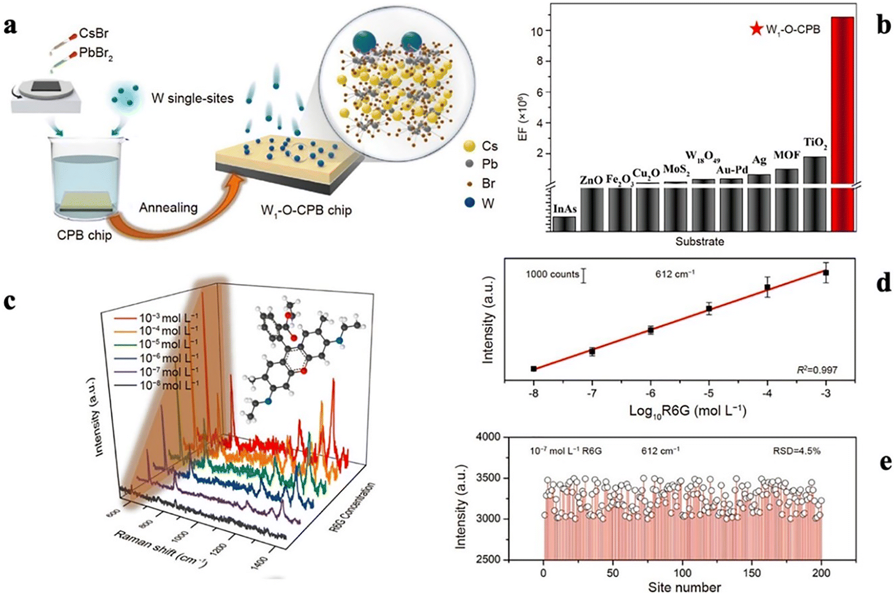 | ||
| Fig. 1 (a) Schematic illustration of the fabrication of a W1-O-CsPb2Br5 (CPB) chip. (b) Comparison of the EFs between the W1-O-CPB chip and other substrates, including plasmon-free semiconductors and single-particle noble metals. (c) Gradually increasing Raman scattering signals recorded for R6G at different concentrations. (d) Calibration curves of the peak intensity versus the logarithmic concentration of R6G measured at 612 cm−1. (e) Signal intensity distributions of R6G@W1-O-CPB. The SERS spectra were obtained by averaging three measurements from five randomly chosen spots. Reprinted with permission from ref. 85. Copyright 2022, Science China Press and Springer-Verlag GmbH Germany, Part of Springer Nature 2022. | ||
Sun et al. found that SERS signals can arise partly from the modulated PL on noble metal surfaces, in contrast the common belief that the PL creates background noise in SERS due to photon scattering.88 Feng et al. developed special single-atom oxide spots on semiconductor chips. They placed single tungsten atom oxide on a lead halide perovskite. This design exploits the ability of the perovskite to generate many photoinduced charges. Many of these single-atom spots on the flat perovskite can attract probe molecules to produce reproducible Raman signals for biological molecules. Furthermore, the single-atom sites can be adjusted to control the CT, inducing higher SERS enhancement. These sites have the capability to precisely transfer photoinduced charges and introduce new energy levels for CT.86
2.2 SERS mechanism of inorganic semiconductors
The different band gap widths of inorganic semiconductors depend on the energy gap between the VB and CB, and the HOMO and LUMO are not the same for different molecules. Therefore, the occurrence of CT between molecules in contact with semiconductor nanomaterials depends on their vibrational coupling modes and on the corresponding energy band positions. The process can be divided into five specific pathways, as follows:63(1) From the HOMO of the molecule to the CB of the semiconductor: after the carriers in the molecule are excited by incident light, the electrons in the HOMO transfer to the CB of the semiconductor and then immediately transition back to the ground state vibrational energy level of the molecule, emitting Raman photons.
(2) From the complex system to the CB of the semiconductor: chemically bound molecules and semiconductors enhance the polarizability of the system, reduce the formation of the CT complex, and enhance the Raman signal of the originally adsorbed molecules.
(3) From the VB of the semiconductor to the LUMO of the molecule: the electrons in the semiconductor VB are transferred to the LUMO of the molecule under incident excitation light and then immediately transition back to the VB of the semiconductor, emitting Raman photons.
(4) From the surface state to the LUMO of the molecule: first, the incident light excites the electrons in the VB of the semiconductor to the surface defects, forming a surface state, from which the electrons are further excited from the surface state to the LUMO of the molecule and then transition back to the surface state, emitting Raman photons in the process.
(5) From the CB of the semiconductor to the HOMO of the molecule: when irradiated with visible light, the electrons in some dye molecules absorb light energy and transition from the ground state to the excited state. Through the resonant tunnelling effect, the electrons are injected into the CB of the semiconductor, and then, the electrons return to the ground state of the molecule, emitting Raman photons.
The traditional theory cannot clearly explain the SERS mechanism in some of the recently developed SERS-active materials. Therefore, researchers should examine the SERS enhancement mechanism in new materials.
(1) Doping inorganic elements into semiconductor materials to promote CT at the substrate-probe molecule interface. Yang et al. presented a guideline for exploring the CT mechanism and introduced a technique to investigate florescence quenching in doped semiconductors (Fig. 2). The VB electrons of ZnO are excited to the newly formed surface state energy level (Ess) and then transferred to the LUMO of 4-MPY under 514.5 nm laser excitation. This process ends with the emission of Raman photons. In contrast, when ZnO is doped with Nd3+ ions, the electrons in the 4f shell of Nd3+ ions transition from the ground state (4I9/2) to the excited states (4F3/2, 4F5/2 + 2H9/2, 4F9/2, and 4G7/2 + 2G5/2). The excited electrons transfer to the LUMO of 4-MPY and release Raman photons in the process of returning to the ground state of Nd3+ ions. This process quenches the fluorescence background of Nd3+ ions and enhances the SERS signal by reducing the number of electrons returning to the ground state. In particular, the energy (2.39 eV) between the LUMO of 4-MPY and the excited state 4F3/2 of Nd3+ ions coincide with the laser energy (2.41 eV) at 514.5 nm to excite CTR.69
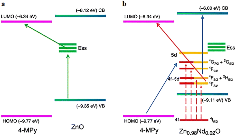 | ||
| Fig. 2 Schematic representations of the CT mechanisms between (a) 4-MPY and ZnO and (b) 4-MPY and Zn0.98Nd0.02O. Reprinted with permission from ref. 69. Copyright 2020, Nature. | ||
(2) Increasing the electron density by utilizing amorphous semiconductor materials to promote CT efficiency. The multiple metastable electronic states found in amorphous semiconductor nanostructures can act as intermediate energy levels within the band gap. This can enhance interfacial CT, leading to impressive SERS activity. Hence, by utilizing the benefits of 2D nanomaterials along with an amorphous structure, the exploration of novel 2D amorphous semiconductor nanomaterials can emerge as a viable approach to enhance the interfacial photoinduced charge transfer (PICT) efficiency. In turn, this increase in PICT efficiency can substantially improve the performance of semiconductor substrates. When the energy levels of the molecules align with the semiconductor substrate, two types of PICT processes become possible. One involves transitions from semiconductor VB states (|V〉) to molecular excited states (|K〉), facilitated by the transition moment μVK. The other requires transitions from ground states (|I〉) of the molecule to CB states (|C〉) of the semiconductor, facilitated by the transition moment μIC. Both processes can gain intensity from either exciton transitions (μVC) or molecular transitions (μIK) due to the Herzberg–Teller coupling term (hCK or hVI).
To gain insight into the SERS phenomenon of amorphous TiO2 nanosheets (a-TiO2 NSs), Wang et al. investigated the surface CT complexes present in both 2D crystalline (c-TiO2) and amorphous (a-TiO2) TiO2 materials. Notably, they found that the electrostatic potential (ESP) on the cross-sectional surface of a-TiO2 was approximately 5.77 V, surpassing the value of approximately 4.81 V for c-TiO2. They also found that this difference in ESP between the two forms of TiO2 is due to the lower coordination number of surface Ti atoms and the abundance of surface oxygen defects in 2D a-TiO2. These properties are related to the extended disordered structure of the amorphous material. While the VB energy of c-TiO2 NSs was approximately −7.4 eV, the VB energy of a-TiO2 NSs was slightly higher at approximately −6.25 eV. As a result, in the 4-MBA@c-TiO2 system, the energy of the CT transition μIC (2.46 eV) exceeded the excitation laser energy (633 nm, 1.96 eV), which hindered the thermodynamically feasible PICT process. In contrast, in the 4-MBA@a-TiO2 system, μIC (1.91 eV) closely matched the excitation laser energy, facilitating efficient PICT between 4-MBA and a-TiO2 NSs. In the 4-MBA@a-TiO2 system, μIC could acquire intensity from neighboring exciton transitions (μVC) within the a-TiO2 NSs due to the robust energy level coupling between the VB of a-TiO2 and the HOMO of 4-MBA.
This mechanism enabled the a-TiO2 NSs to exhibit much stronger SERS activity than c-TiO2 NSs (Fig. 3).66
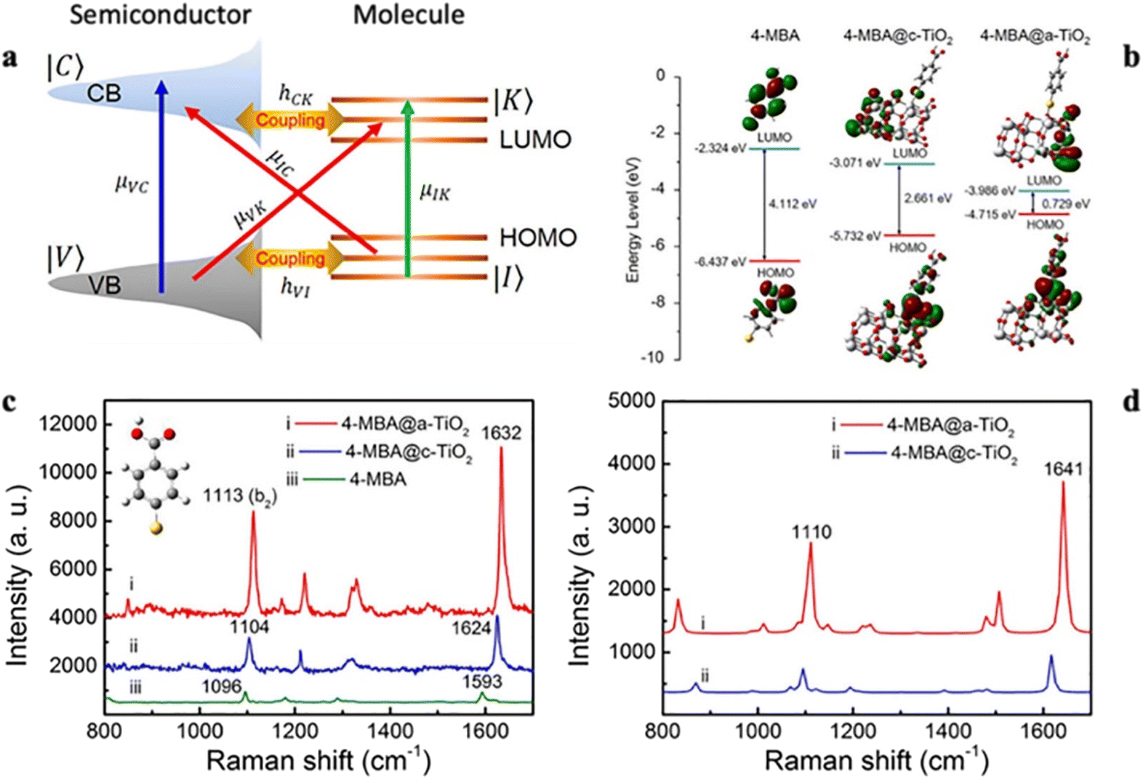 | ||
| Fig. 3 (a) PICT transitions in a semiconductor–molecule system. (b) Schematic diagram of the HOMO and LUMO of 4-MBA, 4-MBA@c-TiO2, and 4-MBA@a-TiO2. (c) Measured SERS spectra of 4-MBA (10−4 M) molecules adsorbed on c- and a-TiO2 NSs and normal Raman spectrum of pure 4-MBA solution (0.1 M) on a Si wafer. (d) Simulated SERS spectra of 4-MBA molecules adsorbed on c- and a-TiO2 NSs. Laser wavelength: 633 nm. Power: 0.8 mW. Lens: 50× objective. Acquisition time: 10 s. Reprinted with permission from ref. 66. Copyright 2019, American Chemical Society. | ||
(3) Coupling exciton and/or molecular resonance to create light-induced CT pathways. The main factor driving the enhancement of SERS in ZrO2 substrates is attributed to CT due to the strong interactions between organophosphates and Zr atoms on the ZrO2 surface. The energy levels of the CB and VB of ZrO2 are 1.97 and 5.19 eV, respectively,89 and the HOMO and LUMO of methyl parathion (MP) are 2.40 and 6.97 eV, respectively.90 Therefore, the energy emitted by the applied laser source (2.33 eV) is not sufficient to bridge these energy gaps.
Vargas-Zamarripa et al. studied the CT transitions induced by the strong adherence between ZrO2 and an organophosphate pesticide (Fig. 4).59 The transition of excited electrons from the VB of ZrO2 to the LUMO of MP and the CT from the HOMO of MP to the CB of ZrO2 are hindered by the significant energy barriers. Notably, the graphene oxide (GO)/ZrO2 substrate including smaller NPs exhibited an increase in SERS intensity of up to two orders of magnitude under similar conditions. In contrast, GO has no band gap and thus has remarkable electron mobility stemming from extensive conjugation and widespread π-electron delocalization.
 | ||
| Fig. 4 (a) Schematic representation of the layer-by-layer SERS-active substrate structure. (b) Raman spectra of MP deposited on different substrates. The MP concentration was 100 mM for GO and glass slide substrates and 10 μM for ZrO2 and GO–ZrO2. The inset shows a magnified view of the distinctive peak at 1345 cm−1. (c) Schematic diagram of the energy level alignment in the GO/ZrO2 substrates for MP detection via SERS. Reprinted with permission from ref. 59. Copyright 2023, Elsevier. | ||
Given that the work function (Φ) of pristine GO is 4.7 eV,91 photoinduced holes conceivably transfer from the ZrO2 NPs to the GO layer, leaving behind trapped electrons that hinder charge recombination. This circumstance leads to a CT pathway in the developed GO/ZrO2 system that involves the initial excitation of ZrO2 NPs from the VB to surface defects. During this process, a surface state energy is generated, which allows electrons to subsequently transfer to the LUMO of the MP. Consequently, Raman photon emission occurs as these electrons return to the ground state. Thus, the increased SERS response in the GO/ZrO2/MP system emerges from the synergistic effects of improved charge separation and efficient CT. These effects result from the interplay of chemical interactions and energy alignment between the substrate and the organophosphate pesticide.59
(4) Enhancing the resonator-based material–light interaction to generate multiple light scattering. Li et al. introduced a novel concept of semiconductor-based colorful SERS-active substrates through Fabry–Pérot (F–P) cavities.92 The F–P cavity, constructed with parallel mirrors, selectively enhances the light field through resonance. This type of substrate can be positioned between materials with different refractive indices. By employing a WO3−x/WO3/W sputtering process, an excellent absorption of over 90% at various incident wavelengths (e.g., 532, 633, and 785 nm) was achieved by adjusting the spacer thickness of the WO3 layer. Notably, this configuration generated visible-light-dependent SERS enhancement, resulting in an EF that was 17 times greater than that of the WO3−x substrate with the same substoichiometric composition but no F–P cavity. Interestingly, this seemingly simple structure forms an unconventional asymmetric F–P nanocavity. As light is reflected between the top and bottom surfaces of the WO3 thin layer, the transmission/reflection of light is amplified or suppressed, producing diverse structural colors. The red film had the highest EF at 6.69 × 10⁷, several times larger than that of the green (3.10 × 10⁷) and yellow (1.72 × 10⁷) films under 532 nm laser excitation. Conversely, the green film had a very high EF of 1.360 × 10⁸, surpassing those of the red (5.53 × 10⁷) and yellow (2.62 × 10⁷) films under 633 nm laser excitation. These differences in signal intensities were logically attributed to the distinct absorbances of the substrates. For resonant absorption, multiple CT transitions allowed by the oxygen vacancy defect level energetically aligned with the incident photons (532 nm, 2.33 eV) are promoted. The combination of enhanced laser absorption and resonant amplification of the electromagnetic field extending across the substrate surface over several nanometers enhances SERS by up to 102 times. This versatile strategy greatly enhances the SERS sensitivity when a diverse range of semiconductor materials are employed as SERS-active substrates.92
(5) Strengthening the electric field by inducing Mie resonance through a specific shape. Ji et al. introduced hollow multishelled semiconductor microstructures as a model configuration for creating SERS-active semiconductor substrates.63 The thorough analysis of the symmetry of vibrational modes appearing in the SERS spectra greatly clarified the foundation of CT coupling based on Herzberg–Teller selection rules. A notable example is V2O5, a narrow-band-gap semiconductor extensively used in energy storage and conversion.63,93 Based on the principles of Mie theory, V2O5 is a promising contender due to its high refractive index and low extinction coefficient. These characteristics of V2O5 make it an effective candidate for generating a strong electric field on the surface of microstructures within the visible-near infrared range.63 To explore the SERS properties of V2O5 microstructures, MB was used as a Raman probe molecule. The lowest detectable concentration of MB for the double-shelled V2O5 spherical microstructure (denoted DS-V) was determined to be 5 × 10⁻⁸ M. Notably, the EF of DS-V reached 1.18 × 10⁶, a value comparable to the highest performance achieved with SERS-active metal oxide substrates enhanced by molecular resonance. The critical energy threshold for charge injection from MB to the CB of V2O5 was estimated to be 1.14–1.21 eV, suggesting that both 532 nm (2.33 eV) and 785 nm (1.58 eV) excitation wavelengths can induce PICT contributions.
According to the Herzberg–Teller selection rules proposed by Lombardi et al. for a molecule–semiconductor system, Γ(Qk) = Γ(μCT)⊥ × Γ(μmol) (24).94Γ(Qk) is the irreducible representation to which the allowed SERS vibrational modes belong. Γ(μCT)⊥ and Γ(μmol) are the irreducible representations to which the CT perpendicular to the surface and the allowed optical transition to the excited state of the molecule belong, respectively. The energy-level diagrams suggest that the enhancement is the result of synergistic effects of CT, exciton resonance, molecular resonance, and the Mie resonance effect. The energy threshold for charge injection from MB into the CB of V2O5 was estimated to be 1.61 eV. As a result, the SERS enhancement is attributed to both CT and Mie resonance contributions under 532 nm laser excitation. However, under 785 nm (1.58 eV) laser excitation, the Mie resonance effect is the main contributor to the SERS enhancement because the photon lacks the energy needed to initiate PICT.63 Furthermore, PICT on the semiconducting K2Ti6O13 nanowire was evidenced by the cytochrome c (Cyt c). The reduced Cyt c was clearly identified on the K2Ti6O13 nanowire due to the electron transfer from the K2Ti6O13 nanowire to the Cyt c. The electron transfer mechanism revealing the importance of energy level matching and electron tunneling from the semiconductor surface to the redox center.95
As mentioned in the previous examples, most semiconductor SERS-active substrates rely on the CT mechanism. However, certain inorganic semiconductor materials, such as transition metal nitrides (TMNs), can produce localized plasmon resonances similar to that of gold due to their high carrier density, which plays a very important role in plasmon generation. Additionally, TMNs can exhibit plasmonic behavior in the visible and near-infrared range under certain conditions, such as variations in optical properties, chemical deposition, and structural size.23,96–98
For example, Sucheewa et al. demonstrated that a hafnium nitride (HfN) thin film created through gas-timed RF magnetron sputtering exhibited an EF of 8.5 × 10⁴ for MB molecules, which was largely attributed to an increased “hot spot” effect. The absorbance of the HfN thin film in the longer wavelength range (approximately 500–900 nm) is advantageous for surface plasmon resonance, which greatly enhances the electromagnetic mechanism on the surface. The small grain size of approximately 15–19 nm and roughness of approximately 0.65–0.93 nm are mainly due to an atomic peening effect. This effect gives the atoms in the thin film enough kinetic energy to enhance the mobility of sputtered atoms condensed at the surface of the film.97 Most importantly, HfN can provide a thermal effect; thus, a stable SERS signal of the analyte can be obtained.98
2.3 Application in different fields
Due to its promising biocompatibility, chemical stability, and reproducibility, semiconductor-based SERS technology has attracted widespread attention in biosystem studies. However, semiconductors typically exhibit lower EFs and sensitivity than conventional SERS-active substrates based on noble metals. As a result, numerous studies have been undertaken to enhance the SERS performance of semiconductors, as discussed earlier.Ma et al. designed a novel 3D flower-like morphology of MoS2 (3D MoS2 nanoflowers) with greatly enhanced light capture and constructed an immunoassay system using 3D MoS2 nanoflowers as the immunoprobe and MoS2@red phosphorus (RP) composite nanoplates as the immunosubstrate. Most importantly, the 3D structure of MoS2 and MoS2@RP composite nanoplates provides synergistic chemical enhancement for ferritin in serum detection based on SERS. Thus, the EF of the proposed system for ferritin is approximately 1.9 × 10⁶ and 8.0 × 10⁶ when using these components as the immunoprobe and immunosubstrate, respectively. Notably, the LOD of the proposed immunoassay is as low as 11.5 pg mL−1. The marked enhancement observed in the MoS2-based system can be attributed to the unique energy level structure of the MoS2@RP composite nanoplates. This structure facilitates more efficient CT between the target molecules and the semiconductor substrate. Furthermore, the flat and expansive surfaces of the immunosubstrate ensured signal stability, as evidenced by a low RSD of 11.3% from the corresponding SERS mapping.99
Recently, we designed ZrO2-based nanoparticles (NPs). Interestingly, by doping Mg and/or Zn ions into the ZrO2 NPs, the SERS activity was significantly improved. During the doping of Mg and/or Zn ions, numerous oxygen vacancies (OV) are generated. The emergence of OV induces the generation of a surface state energy level, providing a channel to facilitate the CT process, which results in an enhancement factor (EF) as high as 104. In addition, qualitative and quantitative analyses were performed using optimal SERS-active substrates with high selectivity and sensitivity to antibiotic drugs, and the detection limit was as low as 10−7 mol L−1.100
In addition, Wang et al. introduced a nonmetallic SERS sandwich immunostructure by utilizing 1T-2H mixed-phase Fe3O4@MoS2 composites and g-C3N4 nanosheets. Their goal was to establish a recyclable assay for tumor markers. The etched g-C3N4 nanosheets demonstrated excellent SERS activity, boasting a low LOD of 3.2 × 10⁻⁶ M and an impressive EF of 7.8 × 10⁶ due to enhanced conductivity. In addition, the proposed sandwich immunostructure exhibited notable results, achieving a high recovery rate surpassing 70% after seven cycles. The uniformity of the distribution was maintained, as indicated by an RSD of 8.8%.56 In another study, Fraser et al. demonstrated the detection of biorelevant molecules on few-layered MoTe2 films via the chemical vapor deposition method. By forming a surface-analyte complex, they were able to measure the analyte down to the nanomolar range, with an EF approaching approximately 104. The smooth and hydrophobic film surfaces facilitated consistent analyte distribution, yielding an RSD of 4.5%.82
Semiconductor materials have been extensively investigated for their photocatalytic properties before being applied as SERS-active substrates; therefore, enhancing the CT capability not only improves their SERS performance but also enhances their photocatalytic efficiency at the same time. Su et al. introduced Ni-doped MoS2 nanoflowers as dual-purpose entities: SERS-active substrates and photocatalysts. They demonstrated impressive photocatalytic degradation efficiencies of 94.23% for MB, 92.1% for malachite green, and 91.9% for methyl orange in 50 min. Furthermore, even in the fifth recycling experiment, the degradation rate for MB remained robust at 92.54%. This sustained performance was attributed to the high specific surface area, low resistance, and pronounced polarity of the 1.0Ni-MoS2 nanoflowers (Fig. 5). Functioning as SERS-active substrates, these nanoflowers exhibited an EF of 3.56 × 10⁵. This remarkable enhancement is ascribed to three pivotal factors: (1) the presence of the 1T-2H mixed phase, which contributes more electrons and significantly promotes the CT process and EM; (2) Ni doping, which strengthens the polarity of the MoS2 nanoflowers and intensifies the interface dipole–dipole interaction with MB molecules; and (3) the increase in the specific surface area of the MoS2 nanoflowers, which enables significant interactions with MB molecules. The utility of Ni-doped MoS2 nanoflowers was extended to the detection of pollutants such as bilirubin, showcasing remarkably sensitive SERS activity with an LOD as low as 10−7 M.101
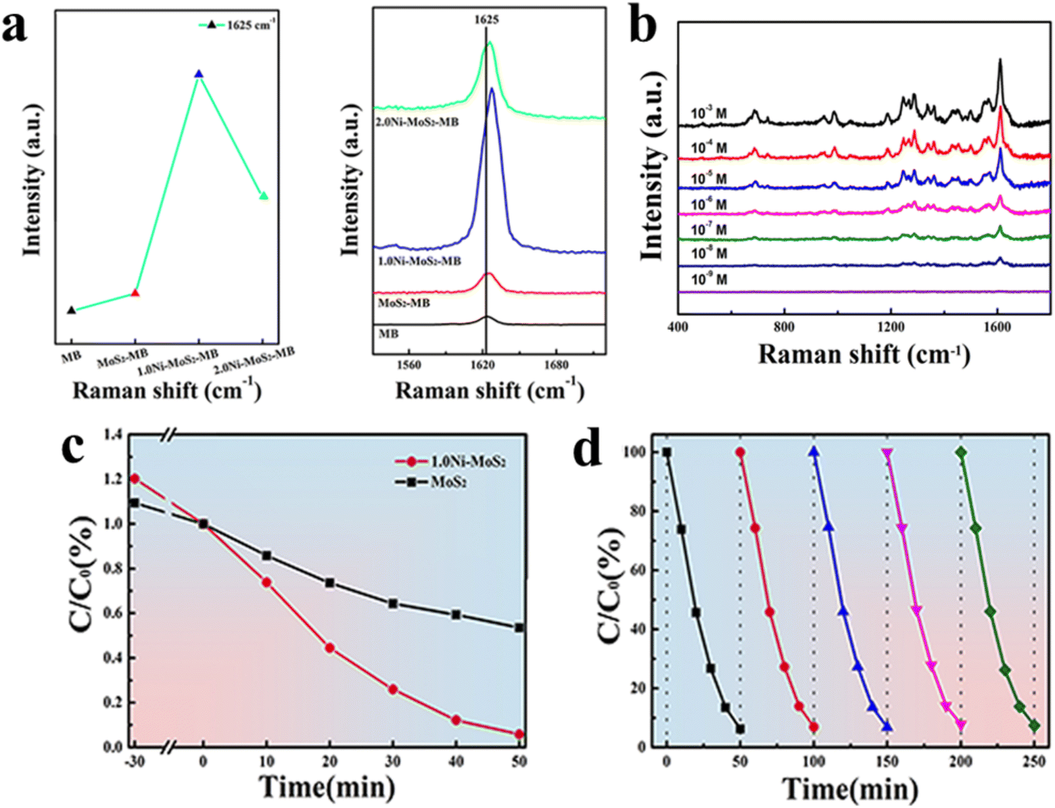 | ||
| Fig. 5 (a) Raman spectrum of MB and SERS spectra of MB molecules on three different substrates: 2.0Ni-MoS2 NF substrates, 1.0Ni-MoS2 NF substrates, and MoS2 NF substrates (left); intensity of the band at 1625 cm−1 of MB molecules adsorbed on different SERS-active substrates (right). (b) SERS spectra recorded from 1.0Ni-MoS2 NF substrates for bilirubin at different concentrations (10−3 to 10−8 M). (c) Variation in the relative MB concentration (C/C0) with irradiation time for different samples. (d) Reusability of 1.0Ni-MoS2 NFs for the degradation process of MB during five cycles. Reprinted with permission from ref. 101. Copyright 2021, Elsevier. | ||
3. Organic semiconductor SERS-active substrates
3.1 Various organic semiconductor SERS-active substrates
Organic semiconductors, organic materials with semiconductor properties, have always been a popular topic in SERS-active substrate research. Initially, pure organic semiconductors were utilized as SERS-active substrates, but their low enhancement ability and detection sensitivity severely limited their applications. Currently, organic semiconductors are combined with metals, inorganic semiconductors and other organic materials to enable sensitive SERS detection. Organic semiconductors can be divided into three categories: organics, polymers, and donor–acceptor complexes. The organic category includes aromatics and metal–organic compounds; polymers include polymers with saturated main chains and conjugated polymers, such as polyphenylene, polyacetylene, polyvinyl carbazole, and polyphenylene sulfide; and CT complexes, such as tetramethyl-p-phenylenediamine complexed with tetracyanoquinone dimethane, consist of two parts: electron donors and electron acceptors.The most prominent example of a pure organic semiconductor is graphene, which was discovered in 2004.102 This material exhibits excellent mechanical, electrical, and optical properties and is widely studied in various applications. In 2010, Ling et al. were the first to discover Raman enhancement on graphene by using pure graphene as a SERS-active substrate and adsorbing common probe molecules such as phthalocyanine (Pc), R6G, protoporphyrin IX (PM), and crystal violet (CV) on the graphene substrate via vacuum evaporation and solution immersion.37 A strong Raman signal was observed on the graphene monolayer with LODs of 10−8–10−10 M.103
The energy and delocalized π-electrons in π-conjugated small organic molecules impart unique chemical, physical, and optoelectronic properties. These conjugated polymer semiconductors can be easily formed into NPs because the solid structure of π-conjugated molecules relies on relatively weak intermolecular interactions. The highly delocalized molecular orbitals are guaranteed to overlap with the effective orbitals of analyte molecules, which can promote the CT process between π-conjugated molecules and analyte molecules, thereby promoting the CM mechanism of SERS. Demirel et al. reported a small molecular 5,5′′′-diperfluorophenyl-2,2′:5′,2′′:5′′,2′′′-quaterthiophene (DFP-4T) nanostructured film composed entirely of a π-conjugated difluorobenzene-substituted tetrathiophene structure that showed a great Raman EF and a low LOD of 10−9 M for MB probe molecules (Fig. 6).104
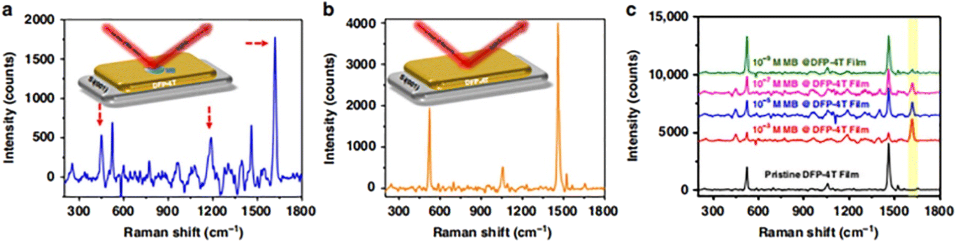 | ||
| Fig. 6 Raman enhancement for nanostructured DFP-4T films. (a) SERS spectrum of the MB probe (10−3 M) on a nanostructured DFP-4T film (characteristic Raman peaks are indicated). (b) Raman spectrum of a pristine nanostructured DFP-4T film. (c) SERS spectra of MB at different concentrations on a nanostructured DFP-4T film. Reprinted with permission from ref. 104. Copyright 2019, Springer Nature. | ||
In recent years, organic donor–acceptor (D–A) complexes have attracted much attention, and organic D–A complexes with multicomponent structures have been designed and synthesized. The multifunctional chemical properties of organic semiconductors provide potential applications for D–A complexes. Organic D–A complexes extend the semiconductor family and promote charge separation and transport in organic field-effect transistors (OFETs) and organic optoelectronics (OPVs). The advantages of semiconductor pads for inducing efficient CT can be applied to SERS. Zhang et al. studied the electrochemical properties of bulk heterojunctions (BHJs) of the local organic polymer semiconductor 3-hexylthiophene (P3HT) and soluble fullerene derivative [6,6]-phenyl-C61-butyric acid methyl ester (PCBM) by Raman spectroscopy (Fig. 7).105
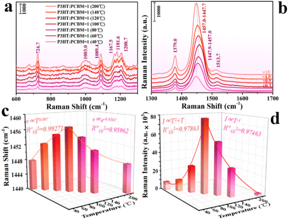 | ||
| Fig. 7 (a and b) Normalized Raman spectra of P3HT:PCBM (weight to weight ratio = 1) after annealing at different temperatures of 40, 60, 80, 100, 120, 140, and 200 °C. (c) Three-dimensional histogram of the frequency shift at approximately 1450 cm−1 and annealing temperature in the P3HT:PCBM system; the curve is the frequency shift and annealing temperature fitting curve. (d) Three-dimensional histogram of the Raman signal peak intensity at 1450 cm−1 and annealing temperature in the P3HT:PCBM system; the curve is the Raman signal peak intensity and annealing temperature fitting curve. Reprinted with permission from ref. 105. Copyright 2021, American Chemical Society. | ||
3.2 SERS mechanisms of organic semiconductors
In contrast to metal materials, semiconductors have no additional plasma layer, and CM is the main enhancement mechanism. CM is a short-range mechanism that is dominated by the amplification effect. A molecular polarization tensor occurs at the semiconductor surface, and analyte molecules are chemically adsorbed through the interfacial CT process. The main difference between organic semiconductors and inorganic semiconductors is the generation of electron–hole pairs, i.e., excitons. Organic semiconductors (conjugated polymers) have relatively low dielectric constants (εr = 2–4). The π electrons in the conjugated double bonds absorb photons and transition from the HOMO to the LUMO. At the same time, holes are formed in the HOMOs of the polymer, and a Coulomb force interaction occurs between electrons and holes, creating an exciton (Frenkel exciton, electron–hole pair) that tightly binds without directly creating a free electron and hole. Exciton resonance is a unique electronic characteristic of semiconductors that is not present in metals. These unique properties make semiconductor substrates completely different from the general structured metal substrates that are effective for almost any molecule. A semiconductor substrate may pave the way for a molecular structure-selective SERS platform. In some cases, the CTR can be coupled with other resonances, such as 3D-driven Mie scattering resonance, nanostructured semiconductor exciton (band gap) resonance and analyte molecular resonance, depending on the electronic structure of semiconductor molecules and excitation laser energy.105–107 For an effective CT process, the orbital wave functions and energies between the frontier orbitals of the analyte and HOMO/LUMO frontier orbitals (organic semiconductors) must be well matched. Currently, research on the SERS mechanism of organic semiconductors is still in continuous development. Researchers have designed a variety of organic semiconductor SERS-active substrates and examined their enhancement mechanisms in depth.Yilmaz et al. expanded SERS to an entirely new field of organic semiconductor substrates.108 They used π-conjugated organic substrates composed of α,ω-diperfluorohexyl tetrathiophene (DFH-4T) to form a thin nanostructured film. Using the MB as a probe molecule, DFH-4T thin films without an additional plasma layer showed an unprecedented Raman signal enhancement of 3.4 × 10³ at a laser wavelength of 785 nm. Through density functional theory (DFT) calculations, they showed that the enhancement of the original organic film is due to the CT transition between the molecule and the organic substrate. That is, the transition of MB molecules at 1.85 eV (668 nm) is close enough to the laser energy to provide an additional transition intensity enhancement compared to the experimental charge. In contrast, changing the substrate to DH-4T (fluorine-free substrate) severely reduced the observed enhancement because the CTR is further from the excitation energy of the laser. Changing the probe molecule to R6G also reduced the enhancement. These observations emphasize the importance of the structural characteristics of the matrix to explain the observed effect.109
Hestand and Spano et al.110 extensively studied the effects of CT and electron coupling of organic H- and J-aggregate semiconductors. The application of theory once again showed that these effects are due to the enhancement of CTR in the molecule–substrate system. These effects occur at the molecular level and between the exciton bands obtained from aggregation, and by coupling the CT transition with the electron coupling effect of the molecule or exciton band in the complex and extending the selection of the substrate to organic semiconductors, the ability to carefully refine the CTR position can be improved.
Using the SERS theory of semiconductor substrates, Lombardi studied the SERS signals of organic J-aggregate substrates.111 Compared to inorganic semiconductors, the exciton band of organic J-aggregates is often very narrow, as is the width of the laser, which considerably simplifies the analysis. The underlying basic theory includes the Born–Oppenheimer approximation and the vibrational coupling proposed by Herzberg and Teller. According to the Herzberg–Teller mixed vibration function, the expression ασρ = A + B + C obtained by Albrecht usually involves the sum of three terms, but Lombardi suggested that very weak coupling is involved in the ground state of aggregates and that for organic J-aggregates, only the B term is applicable. Term B addresses the vibrational selection rule of the harmonic oscillator, which applies to the CT transition from the filled orbital of the molecule (usually HOMO) to the CB of the substrate. For the sake of brevity, term B was slightly simplified to account for the existence of J-aggregates. Although these aggregates are bonded by weak van der Waals bonds, such substrates form conductive bands in the excited state. Due to the formation of the exciton in the excited state, this state is a coherent superposition of the excited state wave functions, and the exciton has a very narrow bandwidth. These excitons have coherence lengths, which are measured by the number of monomers (N) they contain. The electron coupling expression was integrated to obtain the contribution of substrate aggregation to the SERS EF (EF).
Demirel et al. removed and replaced the σ-insulating perfluoroalkyl substituents in DFH-4T with -C6F5, resulting in small intramolecular torsion of the full π-conjugated skeleton. They explored a fluoroarene-modified oligothiophene semiconductor, DFP-4T.104 The design of this molecule enhances the encapsulation of solid molecules, facilitating highly efficient CT in the film and facilitating the overlap of frontier orbital wave functions with those of analyte molecules, which further enhances the SERS performance. To understand the SERS enhancement mechanism in these systems, the excited state properties of complexes formed by analytes (MB) and organic semiconductors were calculated. The results showed that the SERS enhancement of DFP-4T/MB is due to the existence of CT in the excited state, that the absorption cross section is small but not zero, and that the CT state is close to resonance with the laser. Interestingly, the excited state energy of CT is closely related to the HOMO energy of the substrate. However, resonance between the incident light and the CT state is necessary for such a strong enhancement, and when the Raman source is detuned from the CT state, the EF is very small. These results show that the large SERS EFs in the organic system require two characteristics: (1) the CT energy must be tuned to be very close to the incident light resonance, and (2) the semiconductor must be able to effectively π–π stack with the probe molecule to obtain a small but nonzero oscillator strength in the CT state. The obtained DFP-4T thin films show an excellent SERS enhancement of 2.7 × 10⁵, and the lowest detected concentration is as low as 10−9 M, which is comparable to that for the best inorganic semiconductors or even plasmonic metal SERS platforms. These observations not only provide valuable information for the design of future organic semiconductor-based SERS platforms but also provide important progress for the applicability of SERS in the field of biological/chemical sensors.
Based on the study of the SERS mechanism of organic semiconductors, the SERS enhancement of organic semiconductors mainly comes from the molecular resonance of organic semiconductors and the CT between organic semiconductors and probe molecules. Although research on SERS-active substrates of organic semiconductors started late, the enhancement effect at this stage is comparable to that of noble metals and inorganic semiconductors. In addition, based on the unique SERS enhancement mechanism of organic semiconductors, they are also widely used in the fields of biological detection, device performance, medical research, and sensing.
3.3 Application in different fields
Most of the early work on SERS used silver as a substrate because this metal allowed the detection of a single molecule, and the observed maximum EF was as high as 1012. In fact, SERS is currently one of the most promising technologies in the field of spectroscopy. It not only enables ultrasensitivity but can also be used as a qualitative analysis tool for the detection of substances and the identification of trace molecules. To improve sensitivity, SERS-active substrates that are inexpensive, replicable, stable, and reusable under certain conditions must be developed. Since many substrates are made from silver and other precious metals and since a gold standard that meets all of the criteria has not yet been found, ongoing attempts are in progress to find alternative substrates, including semiconductor substrates.Wang et al. fabricated three kinds of interface systems, including a TiO2-Ag-MPY-FePc system similar to a dye-sensitized battery, by an assembly method and analyzed the CT process at the interface with SERS technology.112 By comparing the changes in the SERS spectra of the connecting molecule MPY, they deeply analyzed the different CT processes in the system. TiO2 NPs have a useful ability to change the direction and path of CT in the TiO2-Ag-MPY-FePc interface system, and this work will be important for determining the performance of interface materials in photovoltaic devices using more economical and convenient strategies.
The results showed that electron resonance transition occurs from the HOMO to the LUMO. The excited electrons are then easily transferred to the LUMO of MPY, resulting in an increase in the HOMO and LUMO levels of MPY molecules. Xue et al. reported that the horizontal shift of the MPY molecular orbital increases the energy gap between the Fermi level of Ag NPs and the LUMO level of MPY, which increases the difficulty of CT from Ag NPs to MPY.113 The introduction of FePc suppresses the CT from the Fermi level of Ag NPs to the LUMO level of MPY, which reduces the b2 mode intensity of MPY. Considering that electrons tend to transition from FePc to TiO2 NPs in the TiO2-Ag-MPY-FePc system configuration after electronic assembly, electrons can more easily transfer from FePc to TiO2 NPs under laser excitation.114 Therefore, there may be an additional path for excitation from the HOMO to the LUMO of the coordinated FePc, in which electrons are directly injected into the surface defect state of the defective TiO2. The CT process is suppressed in the Ag-MPY-FePc system but promoted in the defect-rich TiO2 system for excitation lasers of 473, 514, and 633 nm, confirming the proposed mechanism. In summary, this study provides a prospect for the analysis of interface electron transitions in three-interface systems and verifies the significance of TiO2 NPs in regulating the direction of interface electron transfer in solar cell sample systems based on SERS spectra. Thus, this study provides a promising method to initially estimate the electron transfer behavior and optoelectronic properties in optoelectronic devices.
Su et al. studied perovskite materials and succeeded in adsorbing the probe molecule 4-MPY on the single-crystal hybrid perovskite MAPbCl3 and organic–inorganic hybrid CH3NH3PbCl3.115 They also found that the CT between 4-MPY and the perovskite materials reached an EF of 105 under the synergistic action of EM and CT. In addition, they employed 6-mercatoprim (6-MP) to observe and detect the SERS spectrum of the organic–inorganic hybrid perovskite CH3NH3PbBr3. Two probe molecules were adsorbed on CH3NH3PbBr3 by the HS group to achieve CT. Although SERS of perovskite materials established the correlation between CTR-enhanced Raman scattering and the photoelectron response of perovskite materials, there are still some deficiencies in monitoring and regulating CT. The relationship between the carrier transport characteristics (including the carrier lifetime and mobility) and perovskite thickness is a key question for all perovskites, but there are few studies on this topic.
Organic photovoltaic devices are steadily improving in efficiency by reducing the voltage loss, minimizing recombination paths, and increasing the dimensions of carrier paths. However, the transport description for carrier mobility prediction based on charge generation and transport mechanisms in organic semiconductor blends has always been a challenge. Zhang et al. discussed the spectral properties of carrier dynamic processes for poly(3,4-ethylenedioxythiophene) polystyrene sulfonate (PEDOT:PSS)/MB under different bias voltages and conductivities and proposed two possible CT processes under different bias voltages. That is, under laser irradiation at 514 nm, the MB electron absorbs a photon, transitions to a higher energy level, transitions to the corresponding LUMO or PEDOT:PSS level via resonant tunnelling, and then returns to the HOMO of MB, releasing a Raman photon. Another possible CT path is that the electron of PEDOT:PSS absorbs a photon, transfers to the LUMO of MB, and then returns to the HOMO of PEDOT:PSS.116 Based on the above research results, the SERS technique exhibits unique advantages in the study of CT processes and is expected to be an effective means of surface and interface CT process characterization. Although SERS has been used in many basic studies on the CT process, there are few studies on solar cell interface CT.
Organic thin films based on π-conjugated small molecular semiconductors (SMSs) have unique advantages over inorganic and macromolecular organic thin films, including structural versatility, easy and highly controllable synthesis and preparation, and fine-tuning of optoelectronic properties.117–120
Metal-free SMS-based SERS may reveal CM mechanisms that have not yet been explored, as efficient charge/energy transfer between small molecules has implications for a variety of applications, including photoelectron spectroscopy,121,122 lasers,123 chemical sensors and biosensors,124 and biomedical uses.125 Ganesh et al. reported an organic semiconductor SERS probe for detecting single-molecule genomic DNA and cancer stem cells (CSCs), which was precisely reduced to a quantum size using an ultrashort pulsed laser in the presence of nitrogen to study the epigenetic characteristics of CSCs.126 Genomic DNA has key information about structure, molecules, and genetic modifications, which can be used to effectively mark CSCs. A high carrier mobility can increase the effective CT, which can enhance SERS. The detection EF for CV and R6G is 1012, which is 9 orders of magnitude higher than the reported value obtained with organic semiconductors. Four genomic DNA samples, fibroblast (NIH3T3), breast cancer (MDA-MB231), pancreatic cancer (AsPc-1) and lung cancer (H69-AR) samples, were used to validate the practicability of unlabeled quantum organic semiconductor (QOS) sensors. The probe was used for unlabeled genomic DNA detection, which is a method of single-molecule DNA detection. The sensor simultaneously detected the structural, molecular, and gene expression aberrations of genomic DNA at femtomolar concentrations in a single test. In addition to reflecting the differences in genomic DNA between cancer and noncancer cells, QOSs can track the expression of two genes often used as CSC markers. QOSs have the potential to become a new tool for tag-free and ultrasensitive multigenome analysis.126
Recently, SERS platforms based on organic polymer materials have attracted considerable attention due to their low cost, controllable synthesis and manufacture, structural versatility, biocompatibility, and biodegradability. Fularz et al. reported that a substrate based on cellulose nanofibers (CNFs) can be used as a metal-free SERS platform for the detection of porphyrin molecules (Fig. 8). The SERS signals of five different porphyrin molecules were detected, two abnormal band intensities were observed, and the LOD was 10−5 M. This result shows that the cellulose-based platform is more suitable for the detection of porphyrin molecules than conventional semiconductor materials such as GO. The observed enhancement is attributed to the perturbed growth of self-assembled structures on CNFs and the formation of disordered 3D porphyrin clusters.127
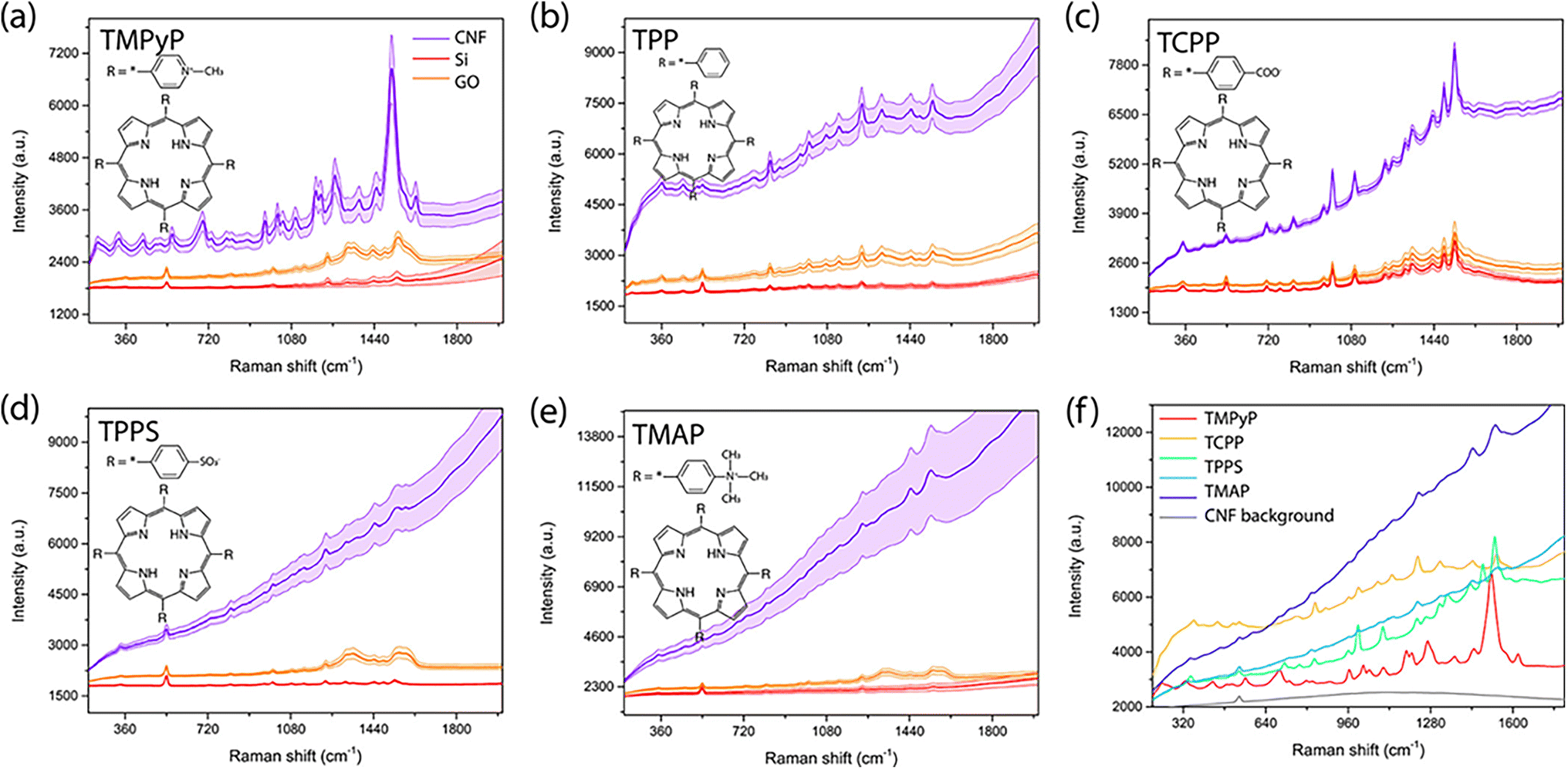 | ||
| Fig. 8 SERS spectra of porphyrin molecules on CNFs compared to the spectra on GO and silicon for 10−3 M (a) TMPyP, (b) TPP, (c) TCPP, (d) TPPS, and (e) TMAP. (f) Spectra for all of the porphyrin molecules on CNFs compared to the Raman background signal of cellulose. Reprinted with permission from ref. 127. Copyright 2021, American Chemical Society. | ||
Organic semiconductors have recently been found to have impressive SERS activity. However, because no candidate materials have been developed and the SERS sensitivity is relatively low, the practical application of SERS detection based on organic materials is still a challenge. Liu et al. explored how to further improve the SERS sensitivity of π-conjugated fluorinated 7,7,8,8-tetracyanoquinodimethane derivatives (FnTCNQ, n = 2, 4) by exploiting the charge localization effect via 2D MoS2 sheets.128 Through the organic/2D heterostructure constructed by FnTCNQ nanostructures grown on 2D MoS2 thin sheets, strong Raman signal enhancement in SERS was realized. In addition, F2TCNQ and F4TCNQ showed different SERS sensitivities due to the number of cyano groups, which resulted in different CT directions. The SERS EF for MB molecules on the optimized F4TCNQ/MoS2 nanocomposite substrate was up to 2.531 × 10⁶, and the LOD was as low as 10−10 M. The SERS results of MB, R6G, and 4-ATP showed that the platform has strong versatility, low cost, good stability, easy preparation, and broad application prospects in trace molecular detection. The study of complex microscopic interactions of organic/2D composite nanomaterials will provide new insights into improving the properties and mechanism of SERS (Fig. 9).
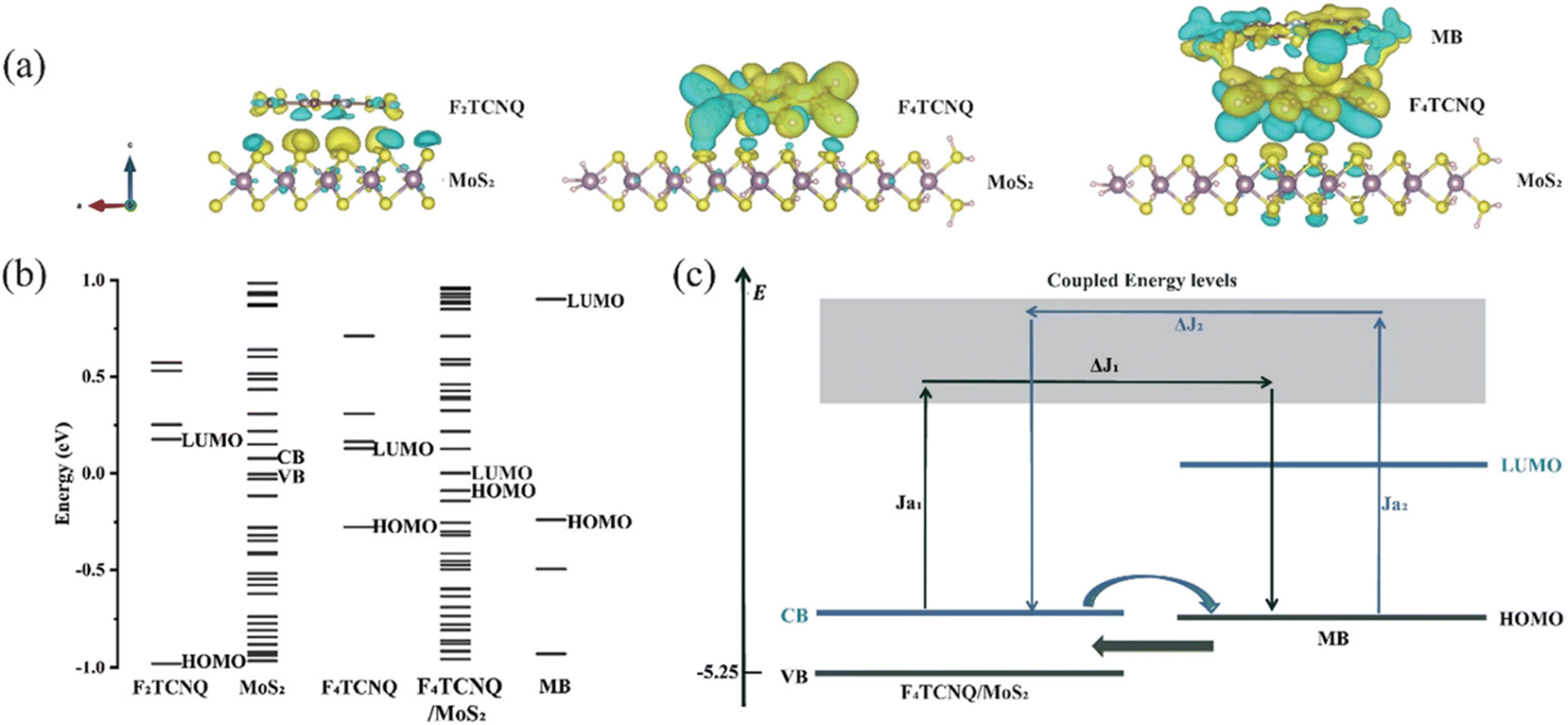 | ||
| Fig. 9 (a) Electron density isosurface plots and (b) molecular orbital energy levels of F2TCNQ/MoS2, F4TCNQ/MoS2, and MB/F4TCNQ/MoS2 composite systems. (c) Schematic view of the CT pathways between the F4TCNQ/MoS2 substrate and MB probe molecule. Reprinted with permission from ref. 128. Copyright 2022, American Chemical Society. | ||
The orbital hybridization between the 2D MoS2 sheet and the C–F bond of FnTCNQ induces charge redistribution in the FnTCNQ/MoS2 composite heterostructure. When combined with MoS2, F2TCNQ, and F4TCNQ show different SERS sensitivities due to the different CT directions and charge locations caused by the different numbers of cyano groups in the composite heterostructure system. The SERS activity of F4TCNQ/MoS2 composites is generally applicable to resonant molecules (R6G), nonresonant molecules (MB), and environmental pollutants (4-ATP) and can be applied to the detection of trace molecules. The EF for MB molecules on the optimized F4TCNQ/MoS2 nanocomposite substrate is as high as 1.124 × 10⁶, and the LOD is as low as 10−10 M. The results show that the inherent SERS activity of π-conjugated organic small molecules can be activated by using the charge localization effect induced by 2D materials. This effect breaks down the application barrier of organic molecules in SERS and enables a step forward in the overall strategy of establishing a direct, sensitive, and universal micromolecular detection SERS platform based on π-conjugated organic materials.
In addition to the above applications, organic SERS-active substrates are used in optoelectronics, photocatalysis, medical diagnosis, forensics, safety, and environmental monitoring. It is believed that with future efforts, organic SERS-active materials will be even more widely used.
4. Conclusion and outlook
In this review, we briefly describe the different kinds of inorganic and organic materials that have been employed for SERS studies and discuss the SERS enhancement mechanisms of different SERS-active materials. For inorganic and organic materials, SERS enhancement occurs mainly due to the molecular resonance of inorganic and organic semiconductors and the CT between semiconductors and probe molecules. The difference between organic semiconductors and inorganic semiconductors is the generation of electron–hole pairs. Therefore, SERS enhancement mechanisms have been extensively explored and gradually improved.However, research on the SERS mechanisms of inorganic and organic semiconductors is still in continuous development. Trace and highly sensitive detection methods are still insufficient. Therefore, based on the current development status of SERS, the following prospects are proposed: (1) the enhancement mechanism of inorganic and organic semiconductors as novel SERS-active substrates in basic research requires further in-depth research and discussion. Due to the diversity of types, preparation processes, and synthesis methods of inorganic and organic semiconductors, semiconductor substrates offer particularly rich possibilities. (2) The exploration of the CT process can be integrated with other disciplines using SERS spectroscopy to solve several practical problems and break down the development barrier between different fields. (3) SERS is being applied in many fields, including food safety, drug testing, and biological testing. However, establishing one or more comprehensive, standardized, and reliable SERS-active substrates and test systems is still a pressing issue.
Author contributions
Sila Jin: writing – original draft; Daxin Zhang: writing – original draft; Bo Yang: writing – review & editing; Shuang Guo: validation; Lei Chen: validation; Young Mee Jung: funding acquisition, writing – review & editing.Conflicts of interest
The authors declare no competing financial interest.Acknowledgements
This work was also supported by the National Research Foundation of Korea (NRF) grants funded by the Korea government (NRF-2021R1A2C2004550 and RS-2023-00243291) and by Korea Basic Science Institute (National Research Facilities and Equipment Center) grant funded by the Ministry of Education (2020R1A6C101A195).References
- M. Fleischmann, P. J. Hendra and A. J. McQuillan, Chem. Phys. Lett., 1974, 26, 163–166 CrossRef.
- D. C. Jeanmarie and R. P. Van Duyne, J. Electroanal. Chem., 1997, 84, 1–20 CrossRef.
- M. G. Albrecht and J. A. Creighton, J. Am. Chem. Soc., 1977, 99, 5215–5217 CrossRef.
- M. Moskovits, J. Chem. Phys., 1978, 69, 4159–4161 CrossRef.
- E. C. Le Ru and P. G. Etchegoin, MRS Bull., 2013, 38, 631–640 CrossRef.
- E. C. Le Ru, E. Blackie, M. Meyer and P. G. Etchegoin, J. Phys. Chem. C, 2007, 111, 13794–13803 CrossRef CAS.
- Q. Chu, W. Wang, S. Guo, E. Park, S. Jin, Y. Park, L. Chen, Y. Liu and Y. M. Jung, ACS Appl. Mater. Interfaces, 2023, 15, 11304–11313 CrossRef CAS.
- X. Wang, S.-C. Huang, S. Hu, S. Yan and B. Ren, Nat. Rev. Phys., 2020, 2, 253–271 CrossRef.
- J. Guo, F. Zeng, J. Guo and X. Ma, J. Mater. Sci. Technol., 2020, 37, 96–103 CrossRef CAS.
- Y. Zhou, Q. Chen, S. Zhong, H. Liu, K. Koh and H. Chen, Biosens. Bioelectron., 2023, 237, 115493 CrossRef CAS.
- X. X. Han, W. Ji, B. Zhao and Y. Ozaki, Nanoscale, 2017, 9, 4847–4861 RSC.
- P. G. Etchegoin, P. D. Lacharmoise and E. Le Ru, Anal. Chem., 2009, 81, 682–688 CrossRef CAS.
- Y. Zhang, Y. Zou, F. Liu, Y. Xu, X. Wang, Y. Li, H. Liang, L. Chen, Z. Chen and W. Tan, Anal. Chem., 2016, 88, 10611–10616 CrossRef CAS PubMed.
- A. I. Pérez-Jiménez, D. Lyu, Z. Lu, G. Liu and B. Ren, Chem. Sci., 2020, 11, 4563–4577 RSC.
- B. Han, S. Guo, S. Jin, E. Park, X. Xue, L. Chen and Y. M. Jung, Nanomaterials, 2020, 10, 1455 CrossRef.
- S. Guo, S. Jin, E. Park, L. Chen, Z. Mao and Y. M. Jung, ACS Appl. Mater. Interfaces, 2021, 13, 5699–5705 CrossRef.
- L. Chen, Y. Jin, S. Guo, E. Park, Y. Xie and Y. M. Jung, Nanoscale, 2023, 15, 16287–16298 RSC.
- B. Han, L. Chen, S. Jin, S. Guo, J. Park, H. S. Yoo, J. H. Park, B. Zhao and Y. M. Jung, J. Phys. Chem. Lett., 2021, 12, 7612–7618 CrossRef PubMed.
- Y. Jin, E. Park, C. Tang, Q. Chu, S. Jin, S. Guo, L. Chen and Y. M. Jung, Spectrochim. Acta A, 2022, 276, 121236 CrossRef.
- S. Guo, S. Jin, E. Park, L. Chen, L. Guo and Y. M. Jung, J. Phys. Chem. C, 2021, 125, 23259–23266 CrossRef.
- N. Ma, L. Chen, T. Jing, X.-Y. Zhang, B. Han, X. Xue, Y. Zhang and B. Zhao, J. Phys. Chem. C, 2019, 123, 28846–28851 CrossRef.
- X. Zhao, Q. Chu, S. Guo, E. Park, S. Jin, L. Chen, Y. Liu and Y. M. Jung, Spectrochim. Acta A, 2023, 286, 121995 CrossRef PubMed.
- G. Song, S. Cong and Z. Zhao, Chem. Sci., 2022, 13, 1210–1224 RSC.
- H. Yamada, Y. Yamamoto and N. Tani, Chem. Phys. Lett., 1982, 86, 397–400 CrossRef.
- W. Ji, L. Li, W. Song, X. Wang, B. Zhao and Y. Ozaki, Angew. Chem., Int. Ed., 2019, 58, 14391–14769 CrossRef.
- Z. Sun, B. Zhao and J. R. Lombardi, Appl. Phys. Lett., 2007, 91, 221106 CrossRef.
- A. Musumeci, D. Gosztola, T. Schiller, N. M. Dimitrijevic, V. Mujica, D. Martin and T. Rajh, J. Am. Chem. Soc., 2009, 131, 6040–6041 CrossRef CAS.
- X. Jiang, D. Yin, M. Yang, J. Du, W. Wang, L. Zhang, L. Yang, X. Han and B. Zhao, Appl. Surf. Sci., 2019, 487, 938–944 CrossRef CAS.
- W. Ji, Y. Wang, I. Tanabe, X. Han, B. Zhao and Y. Ozaki, Chem. Sci., 2015, 6, 342–348 RSC.
- J. S. Teguh, F. Liu, B. Xing and E. K. Yeow, Chem. – Asian J., 2012, 7, 975–981 CrossRef CAS.
- L. Jiang, T. You, P. Yin, Y. Shang, D. Zhang, L. Guo and S. Yang, Nanoscale, 2013, 5, 2784–2789 RSC.
- H. Yamada and Y. Yamamoto, Surf. Sci., 1983, 134, 71–90 CrossRef CAS.
- D. Qi, L. Lu, L. Wang and J. Zhang, J. Am. Chem. Soc., 2014, 136, 9886–9889 CrossRef CAS.
- L. Dawei, W. Jian, X. Houwen, S. Xu and L. Fan-chen, Spectrochim. Acta A, 1987, 43, 379–382 CrossRef.
- C. Mou, D. Chen, X. Wang, B. Zhang, T. He, H. Xin and F.-C. Liu, Spectrochim. Acta A, 1991, 47, 1575–1581 CrossRef.
- H. Zhang, H. Xin, T. He and F. Liu, Spectrochim. Acta A, 1991, 47, 927–932 CrossRef.
- X. Ling, L. Xie, Y. Fang, H. Xu, H. Zhang, J. Kong, M. S. Dresselhaus, J. Zhang and Z. Liu, Nano Lett., 2010, 10, 553–561 CrossRef PubMed.
- X. Ling and J. Zhang, Small, 2010, 6, 2020–2025 CrossRef PubMed.
- P. Guo, D. Sikdar, X. Huang, K. J. Si, W. Xiong, S. Gong, L. W. Yap, M. Premaratne and W. Cheng, Nanoscale, 2015, 7, 2862–2868 RSC.
- B. Yang, S. Jin, S. Guo, Y. Park, L. Chen, B. Zhao and Y. M. Jung, ACS Omega, 2019, 4, 20101–20108 CrossRef.
- D.-Y. Wu, J.-F. Li, B. Ren and Z.-Q. Tian, Chem. Soc. Rev., 2008, 37, 1025–1041 RSC.
- P. Karthick Kannan, P. Shankar, C. Blackman and C.-H. Chung, Adv. Mater., 2019, 31, 1803432 CrossRef PubMed.
- B. Yang, Y. Wang, S. Guo, S. Jin, L. Chen and Y. M. Jung, Bull. Korean Chem. Soc., 2021, 42, 1411–1418 CrossRef CAS.
- Z. Lian, C. Lu, Q. Sun, J. Cheng, C. Miao and Z. Chen, J. Raman Spectrosc., 2023, 54, 580–586 CrossRef CAS.
- X. Xiu, L. Hou, J. Yu, S. Jiang, C. Li, X. Zhao, Q. Peng, S. Qiu, C. Zhang, B. Man and Z. Li, Nanophotonics, 2021, 10, 1529–1540 CrossRef CAS.
- P. A. Mosier-Boss, Nanomaterials, 2017, 7, 142 CrossRef PubMed.
- X. Wang and L. Guo, Angew. Chem., Int. Ed., 2020, 59, 4231–4239 CrossRef CAS.
- C. Ji, J. Lu, B. Shan, F. Li, X. Zhao, J. Yu, S. Xu, B. Man, C. Zhang and Z. Li, J. Phys. Chem. Lett., 2022, 13, 8864–8871 CrossRef CAS PubMed.
- X. Tan, J. Melkersson, S. Wu, L. Wang and J. Zhang, ChemPhysChem, 2016, 17, 2630–2639 CrossRef CAS.
- H. Wu, H. Wang and G. Li, Analyst, 2017, 142, 326–335 RSC.
- L. Yang, Y. Peng, Y. Yang, J. Liu, Z. Li, Y. Ma, Z. Zhang, Y. Wei, S. Li and Z. Huang, ACS Appl. Nano Mater., 2018, 1, 4516–4527 CrossRef CAS.
- H. Qiu, M. Wang, L. Zhang, M. Cao, Y. Ji, S. Kou, J. Dou, X. Sun and Z. Yang, Sens. Actuators B: Chem., 2020, 320, 128445 CrossRef CAS.
- R. Wang, H. Liu, T. Xu, Y. Zhang, C. Gu and T. Jiang, Biosens. Bioelectron., 2023, 227, 115160 CrossRef PubMed.
- Z. He, T. Rong, Y. Li, J. Ma, Q. Li, F. Wu, Y. Wang and F. Wang, ACS Nano, 2022, 16, 4072–4083 CrossRef.
- S. Jin, E. Park, S. Guo, Y. Park, L. Chen and Y. M. Jung, CrystEngComm, 2021, 23, 8443–8450 RSC.
- Samriti, K. Shukla, R. Gupta, R. K. Gupta and J. Prakash, Environ. Sci. Pollut. Res., 2023, 30, 34054–34068 CrossRef PubMed.
- B. P. Majee, Bhawna and A. K. Mishra, Mater. Res. Express, 2020, 6, 1250j1 CrossRef.
- E. Proniewica, A. Tąta, A. Wójcik, M. Starowicz, J. Pacek and M. Molenda, Phys. Chem. Chem. Phys., 2020, 22, 28100–28114 RSC.
- M. Vargas-Zamarripa, A. A. Rivera, U. Sierra, P. Salas, A. H. Serafín-Muñoz and G. Ramírez-García, Chemosphere, 2023, 320, 138081 CrossRef CAS.
- J. Sui, D. Liu, C. Wang, L. Wang, B. Zhong and Y. Ma, J. Alloys Compd., 2023, 934, 167864 CrossRef CAS.
- H. Liu, Q. Li, Y. Ma, S. Wang, Y. Wang, B. Zhao, L. Zhao, Z. Jiang, L. Xu and W. Ruan, Spectrochim. Acta A, 2023, 303, 123168 CrossRef CAS PubMed.
- C. He, L. Jiang, R. Yuan and X. Yang, Sens. Actuators B: Chem., 2023, 374, 132777 CrossRef CAS.
- W. Ji, L. Li, J. Guan, M. Mu, W. Song, L. Sun, B. Zhao and Y. Ozaki, Adv. Opt. Mater., 2021, 9, 2101866 CrossRef CAS.
- X. Wang, J. Li, Y. Shen and A. Xie, Appl. Surf. Sci., 2020, 504, 144073 CrossRef CAS.
- R. He, H. Lai, S. Wang, T. Chen, F. Xie, Q. Chen, P. Liu, J. Chen and W. Xie, Appl. Surf. Sci., 2020, 507, 145116 CrossRef CAS.
- X. Wang, W. Shi, S. Wang, H. Zhao, J. Lin, Z. Yang, M. Chen and L. Guo, J. Am. Chem. Soc., 2019, 141, 5856–5862 CrossRef CAS.
- X. Jiang, Q. Sang, M. Yang, J. Du, W. Wang, L. Yang, X. Han and B. Zhao, Phys. Chem. Chem. Phys., 2019, 21, 12850–12858 RSC.
- L. Guo, X. Zhang, P. Li, R. Han, Y. Liu, X. Han and B. Zhao, New J. Chem., 2019, 43, 230–237 RSC.
- S. Yang, J. Yao, Y. Quan, M. Hu, R. Su, M. Gao, D. Han and J. Yang, Light: Sci. Appl., 2020, 9, 117 CrossRef CAS PubMed.
- E. Hutter and J. H. Fendler, Adv. Mater., 2004, 16, 1685–1706 CrossRef CAS.
- R. Himstedt, P. Rusch, D. Hinrichs, T. Kodanek, J. Lauth, S. Kinge, L. D. A. Siebbeles and D. Dorfs, Chem. Mater., 2017, 29, 7371–7377 CrossRef CAS.
- Z. Wang, C. Liao, C. Yang, X. Mao, H. Zhang, G. He, F. Gou, K. Zhang, F. Zhao and Z. Ye, J. Phys. Chem. Solids, 2023, 175, 111207 CrossRef CAS.
- G. Song, H. Sun, J. Chen, Z. Chen, B. Liu, Z. Liu, S. Cong and Z. Zhao, Anal. Chem., 2022, 94, 5048–5054 CrossRef CAS PubMed.
- S. Liu, X. Zhang, J. Zhang, Z. Lei, X. Liang and B. Chen, Sci. China Mater., 2016, 59, 1051–1061 CrossRef CAS.
- G. Eda, H. Yamaguchi, D. Voiry, T. Fujita, M. Chen and M. Chhowalla, Nano Lett., 2011, 11, 5111–5116 CrossRef CAS.
- Z. Qian, L. Jiao and L. Xie, Chin. J. Chem., 2020, 38, 753–760 CrossRef CAS.
- G. Gao, Y. Jiao, F. Ma, Y. Jiao, E. Waclawik and A. Du, J. Phys. Chem. C, 2015, 119, 13124–13128 CrossRef CAS.
- X. Gan, L. Y. S. Lee, K.-Y. Wong, T. W. Lo, K. H. Ho, D. Y. Lei and H. Zhao, ACS Appl. Energy Mater., 2018, 1, 4754–4765 CrossRef CAS.
- C. Hu and L. Dai, Adv. Mater., 2019, 31, 1804672 CrossRef.
- C. J. Boyle, M. Upadhyaya, P. Wang, L. A. Renna, M. Lu-Díaz, S. P. Jeong, N. Hight-Huf, L. Korugic-Karasz, M. D. Barnes, Z. Aksamija and D. Venkataraman, Nat. Commun., 2019, 10, 2827 CrossRef.
- R. Su, S. Yang, D. Han, M. Hu, Y. Liu, J. Yang and M. Gao, J. Colloid Interface Sci., 2023, 635, 1–11 CrossRef CAS PubMed.
- J. P. Fraser, P. Postnikov, E. Miliutina, Z. Kolska, R. Valiev, V. Švorčík, O. Lyutakov, A. Y. Ganin and O. Guselnikova, ACS Appl. Mater. Interfaces, 2020, 12, 47774–47783 CrossRef CAS PubMed.
- T. Jena, T. M. Hossain, U. Nath, M. Sarma, H. Sugimoto, M. Fujii and P. K. Giri, npj 2D Mater. Appl., 2023, 7, 8 CrossRef CAS.
- M. W. Barsoum, Prog. Solid State Chem., 2000, 28, 201–281 CrossRef CAS.
- B. Soundiraraju and B. K. George, ACS Nano, 2017, 11, 8892–8900 CrossRef PubMed.
- R. Feng, Q. Miao, X. Zhang, P. Cui, C. Wang, Y. Feng, L. Gan, J. Fu, S. Wang and Z. Dai, Sci. China Mater., 2022, 65, 1601–1614 CrossRef PubMed.
- J. Wang, C. Qiu, H. Pang, J. Wu, M. Sun and D. Liu, J. Mater. Chem. C, 2021, 9, 9011–9020 RSC.
- J. Sun, H. Hu, D. Zheng, D. Zhang, Q. Deng, S. Zhang and H. Xu, ACS Nano, 2018, 12, 10393–10402 CrossRef.
- P. Ji, Z. Wang, X. Shang, Y. Zhang, Y. Liu, Z. Mao and X. Shi, Front. Chem., 2019, 7, 245 CrossRef.
- K. He, Z. Li, L. Wang, Y. Fu, H. Quan, Y. Li, X. Wang, S. Gunasekaran and X. Xu, ACS Appl. Mater. Interfaces, 2019, 11, 26250–26260 CrossRef CAS PubMed.
- S. Ji, B. K. Min, S. K. Kim, S. Myung, M. Kang, H.-S. Shin, W. Song, J. Heo, J. Lim, K.-S. An, I.-Y. Lee and S. S. Lee, Appl. Surf. Sci., 2017, 419, 252–258 CrossRef CAS.
- F. Li, X. Mu, X. Tang, G. Song, H. Sun, X. Zha, P. Sun, J. Fang, D. Hu and S. Cong, Angew. Chem., Int. Ed., 2023, 62, e202218055 CrossRef CAS PubMed.
- N. Wu, W. Du, G. Liu, Z. Zhou, H.-R. Fu, Q. Tang, X. Liu and Y.-B. He, ACS Appl. Mater. Interfaces, 2017, 9, 43681–43687 CrossRef CAS PubMed.
- J. R. Lombardi and R. L. Birke, J. Phys. Chem. C, 2014, 118, 11120–11130 CrossRef CAS.
- L. Chen, J. Tang, H. Ma, S. Jin, X. Xue, X. X. Han and Y. M. Jung, Biosens. Bioelectron., 2021, 191, 113452 CrossRef CAS PubMed.
- M. Liu, S. Cheng, X. Du, J. Li, Q. Peng, C. Zhao, Y. Wang and X. Xiu, Opt. Express, 2023, 31, 38699–38714 CrossRef PubMed.
- N. Sucheewa, W. Wongwiriyapan, A. Klamchuen, M. Obata, M. Fujishige, K. Takeuchi, T. Lertvanithphol, T. Wutikhun, S. Kullyakool, W. Auttasiri, N. Sowasod, T. Prataen, W. Tanthapanichakoon and J. Nukeaw, Crystals, 2022, 12, 78 CrossRef.
- K. Girel, A. Burko, S. Zavatski, A. Barysiuk, K. Litvinova, E. Eganova, A. Tarasov, D. Novikov, S. Dubkov and H. Bandarenka, Appl. Phys. A: Mater. Sci. Process., 2023, 129, 294 CrossRef.
- J. Ma, W. Dong, T. Xu, G. Wei, C. Gu and T. Jiang, Analyst, 2023, 148, 1752–1763 RSC.
- J. Xu, X. Shi, M. Yi, Y. Chi, S. Guo, Z. Mao, B. Zhao and Y. M. Jung, Appl. Surf. Sci., 2023, 639, 158256 CrossRef.
- R. Su, Y. Quan, S. Yang, M. Hu, J. Yang and M. Gao, J. Alloys Compd., 2021, 886, 161268 CrossRef CAS.
- K. S. Novoselov, A. K. Geim, S. V. Morozov, D.-E. Jiang, Y. Zhang, S. V. Dubonos, I. V. Grigorieva and A. A. Firsov, Science, 2004, 306, 666–669 CrossRef CAS PubMed.
- G. Demirel, H. Usta, M. Yilmaz, M. Celik, H. A. Alidagi and F. Buyukserin, J. Mater. Chem. C, 2018, 6, 5314–5335 RSC.
- G. Demirel, R. L. Gieseking, R. Ozdemir, S. Kahmann, M. A. Loi, G. C. Schatz, A. Facchetti and H. Usta, Nat. Commun., 2019, 10, 5502 CrossRef CAS PubMed.
- D. Zhang, S. Yang, W. Zhao, L. Yang, Y. Liu, M. Wei, L. Chen and J. Yang, ACS Appl. Energy Mater., 2021, 4, 8360–8367 CrossRef CAS.
- D. Savateeva, D. Melnikau, V. Lesnyak, N. Gaponik and Y. P. Rakovich, J. Mater. Chem., 2012, 22, 10816–10820 RSC.
- J. Zhang, W. Xu, P. Sheng, G. Zhao and D. Zhu, Acc. Chem. Res., 2017, 50, 1654–1662 CrossRef PubMed.
- M. Yilmaz, E. Babur, M. Ozdemir, R. L. Gieseking, Y. Dede, U. Tamer, G. C. Schatz, A. Facchetti, H. Usta and G. Demirel, Nat. Mater., 2017, 16, 918–924 CrossRef PubMed.
- J. R. Lombardi, Nat. Mater., 2017, 16, 878–880 CrossRef PubMed.
- N. J. Hestand and F. C. Spano, Chem. Rev., 2018, 118, 7069–7163 CrossRef PubMed.
- J. R. Lombardi, Chem. Phys. Lett., 2020, 751, 137553 CrossRef.
- Y. Wang, J. Liu, Y. Ozaki, Z. Xu and B. Zhao, Angew. Chem., Int. Ed., 2019, 58, 8172–8176 CrossRef CAS PubMed.
- X. Xue, D. Xu, W. Ruan, L. Chen, L. Chang and B. Zhao, RSC Adv., 2015, 5, 64235–64239 RSC.
- Y. Wang, Z. Yu, W. Ji, Y. Tanaka, H. Sui, B. Zhao and Y. Ozaki, Angew. Chem., Int. Ed., 2014, 53, 13866–13870 CrossRef CAS PubMed.
- X. Su, H. Ma, H. Wang, X. Li, X. X. Han and B. Zhao, Chem. Commun., 2018, 54, 2134–2137 RSC.
- X.-Y. Zhang, S. Yang, L. Yang, D. Zhang, Y. Sun, Z. Pang, J. Yang and L. Chen, Chem. Commun., 2020, 56, 2779–2782 RSC.
- A. Facchetti, Chem. Mater., 2011, 23, 733–758 CrossRef CAS.
- J. A. Labastide, H. B. Thompson, S. R. Marques, N. S. Colella, A. L. Briseno and M. D. Barnes, Nat. Commun., 2016, 7, 10629 CrossRef CAS PubMed.
- A. Bhakat and A. Chattopadhyay, Adv. Opt. Mater., 2023, 11, 2301776 CrossRef.
- S. Guo, Y. Park, E. Park, S. Jin, L. Chen and Y. M. Jung, Angew. Chem., Int. Ed., 2023, 62, e202306709 CrossRef CAS PubMed.
- R. Capelli, S. Toffanin, G. Generali, H. Usta, A. Facchetti and M. Muccini, Nat. Mater., 2010, 9, 496–503 CrossRef PubMed.
- A. Fularz, S. Almohammed and J. H. Rice, ACS Sustainable Chem. Eng., 2022, 10, 508–520 CrossRef.
- H. S. Kavazoi, C. S. Martin, M. D. Maximino, M. S. Pereira, M. L. Rodríguez-Méndez and P. Alessio, Phys. Chem. Chem. Phys., 2023, 25, 26999–27007 RSC.
- L. L. Tian, C. Chen, J. Gong, Q. Han, Y. J. Shi, M. Q. Li, L. Cheng, L. Wang and B. Dong, Sensors, 2023, 23, 4641 CrossRef PubMed.
- Y. F. Chen, Q. An, K. X. Teng, C. Liu, F. W. Sun and G. T. Li, Chem. – Asian J., 2023, 18, e202201194 CrossRef PubMed.
- S. Ganesh, K. Venkatakrishnan and B. Tan, Nat. Commun., 2020, 11, 1135 CrossRef CAS PubMed.
- A. Fularz, S. Almohammed and J. H. Rice, ACS Sustain. Chem. Eng., 2021, 9, 16808–16819 CrossRef CAS.
- M. Liu, W. Liu, W. Zhang, P. Duan, M. Shafi, C. Zhang, X. Hu, G. Wang and W. Zhang, ACS Appl. Mater. Interfaces, 2022, 14, 56975–56985 CrossRef CAS PubMed.
Footnote |
| † These authors contributed equally to this work. |
| This journal is © The Royal Society of Chemistry 2024 |