
 Open Access Article
 This Open Access Article is licensed under a Creative Commons Attribution-Non Commercial 3.0 Unported Licence
Liquid phase epitaxy of CuGaO2 on GaN: P–N heterostructure for photocatalytic water splitting†
Hadi
Sena
 *ab,
Sho
Kitano
c,
Hiroki
Habazaki
c and
Masayoshi
Fuji
ab
*ab,
Sho
Kitano
c,
Hiroki
Habazaki
c and
Masayoshi
Fuji
ab
aAdvanced Ceramic Research Center, Nagoya Institute of Technology, Tajimi 507-0033, Japan
bDepartment of Life Science and Applied Chemistry, Nagoya Institute of Technology, Tajimi 507-0071, Japan
cDivision of Applied Chemistry, Faculty of Engineering, Hokkaido University, Sapporo 060-8628, Japan
First published on 8th August 2023
Abstract
Semiconductor photocatalytic water splitting is a promising method to address the worldwide energy issues. Fast carrier recombination and the limited visible-light absorption are two main challenges to be overcome, and designing p–n heterojunctions is an effective solution. In this study, two direct band gap semiconductors are selected to form a p–n heterojunction. The results show that liquid phase epitaxy of a thick film p-type CuGaO2 on an n-type GaN substrate is effective for the splitting of water into hydrogen and oxygen.
Introduction
Solar water splitting is a promising method for the direct conversion of solar energy into chemical fuels like hydrogen and oxygen. Photochemical water splitting is advantageous over photoelectrochemical water splitting, in which the counter electrode is mounted on the photocatalyst surface, known as the co-catalyst.1–3 Therefore, it is a cheap wireless reaction system, no external bias is required, and efficiency is not restricted by the low current conduction issues. The efficiency of most photocatalysts under sunlight is usually low because (i) they have a large bang gap and they are not able to absorb visible light, which accounts for about 50% of the solar spectrum, (ii) the photocatalyst undergoes photo-corrosion after a certain period of reaction, (iii) photo-excited carriers recombine radiatively or non-radiatively before diffusing to the surface, usually being trapped at defect states, (iv) a severe upward band bending occurs at the surface of the n-type photocatalyst and the energy barrier caused by the band bending repels the photo-excited electrons toward the bulk region.4,5A p–n heterostructure consisting of p-type and n-type semiconductors in contact is an effective architecture for efficient charge separation and collection.6,7 They form a p–n junction with a space-charge region at the interface due to the diffusion of electrons and holes, creating a built-in potential. This built-in potential directs the electrons and holes to move in the opposite direction. Upon irradiation by light sources with energies higher than the band gap, the photo-generated electron–hole pairs can be easily separated by the built-in electric field. As a consequence, the electrons are transferred to the conduction band of the n side and the holes to the valence band of the p side.
Copper gallium oxide (CuGaO2) with the general structure of ABO2 (A: Pt, Pd, Cu, Ag, and B: Al, Ga, In, Sc, Fe, Y, La) was first introduced by Omata et al.8 It was shown that CuGaO2 had a direct band gap in the visible light region with a wurtzite crystal structure and p-type feature. Since then, the material has been mainly used as a solar cell absorber thanks to its high hole mobility and stability.9–11 In this study, we designed a p–n heterostructure of CuGaO2 and gallium nitride (GaN). GaN is also a direct band gap semiconductor with an intrinsic n-type feature. It possesses remarkable electronic and optoelectronic properties, with a tunable direct band gap from 0.7 to 6.2 eV, and high-electron mobility (>103 cm2 V−1 s−1). All these superior properties inspired us to design a p–n junction of two direct band gap semiconductors for efficient photocatalytic water splitting reaction. In this study, we will show how the p–n heterojunction is effective for water splitting hydrogen/oxygen generation reactions, while neither CuGaO2 nor GaN are capable of splitting water efficiently.
Experimental section
CuGaO2 thick films were grown by the liquid phase epitaxy method on a c-plane GaN wafer with a thickness of 420 μm, the dislocation density of 4.6 × 106 cm−2, miscut angle of 0.5° towards the 11−20 direction, and donor concentration of 3 × 1016 cm−3. Alumina crucibles were used to hold the growth solution and reactants, in which 99.9%-pure CuCl2 was chosen as the bath solvent and Cu source. 5 mmol of Ga2O3 powder (99.99% purity) was used as the solute and was mixed with 45 mmol CuCl2. The mixture of CuCl2 and Ga2O3 was placed on the epi-ready GaN substrate, which was previously cut into a rectangle of 1 × 2 cm. The term “epi-ready” refers to the surface roughness of the substrate, which typically has a root mean square (RMS) value of less than 1 nm. No further polishing was performed on the substrate, and the film was grown on the substrate as purchased. The crucible was heated to 800 °C at the rate of 40 °C min−1, held for 3 h, and cooled to room temperature at the rate of 2 °C min−1. The obtained powders and substrate were thoroughly washed with distilled water, and the substrate was further ultrasonicated in water for 10 min in order to make sure no unreacted powder was present on the surface of the substrate.The surface morphology of the film was observed by a differential interference contrast (DIC) optical microscope, laser confocal imaging microscope, scanning electron microscope (SEM), and atomic force microscope (AFM) in tapping mode at the top view and the bird's eye view. X-ray diffraction (XRD) and Raman spectroscopy with a 532 nm laser were employed to identify the crystalline structure and orientation of the as-grown films and powders. The SEM equipped with an energy dispersive X-ray spectrometer (EDS) with a lateral resolution of 2 nm and an acceleration voltage of 20 kV was used for composition analysis. UV-Vis diffuse reflectance spectroscopy was used to estimate the band gaps. Photocatalytic hydrogen evolution was examined in a solution of 50 mg powder or 1 cm × 2 cm substrate, 0.5 mL CH3OH, 4.5 mL H2O and 133 μL H2PtCl6.6H2O (19.5 mM) under a Xenon light source. The photocatalytic reaction for O2 evolution from an aqueous silver nitrate solution (0.05 mol L−1) was carried out in a test tube. For both tests, Ar gas was bubbled for 30 min for removing air dissolved in water. The temperature of the reactions was maintained at room temperature by using a water bath. The quantity of the evolved gases was determined by a gas chromatograph (thermal conductivity detector; molecular sieve 5 Å column packing with Ar carrier gas for H2 test, and He carrier gas for O2 test). A schematic illustration of the experiment setup is shown in Fig. S1 (ESI†). The apparent quantum efficiency (AQE) was evaluated using a 380 nm monochromatic light source. The active surface area of the samples was measured by the adsorption isotherms of N2 at 77 K by the Brunauer–Emmett–Teller (BET) method. Cathodoluminescence (CL, LS-100-EM-TYPE2, HORIBA) attached to the FE-SEM was measured under 15 kV at room temperature for the estimation of the carrier recombination rate.
Results and discussion
Fig. 1 shows a 3D bird's eye view image of CuGaO2 film grown on the GaN substrate observed by a DIC optical microscope and laser microscope. It is evident that the epitaxial structures are grown perpendicular to the 0001 plane of the GaN substrate with the root mean square (RMS) surface roughness of 260 nm in the scan area of 256 μm × 256 μm. The surface roughness was well consistent with the AFM results, where the roughness was estimated to be 277 nm in the scan area of 2 μm × 2 μm, as shown in Fig. S2 (ESI†).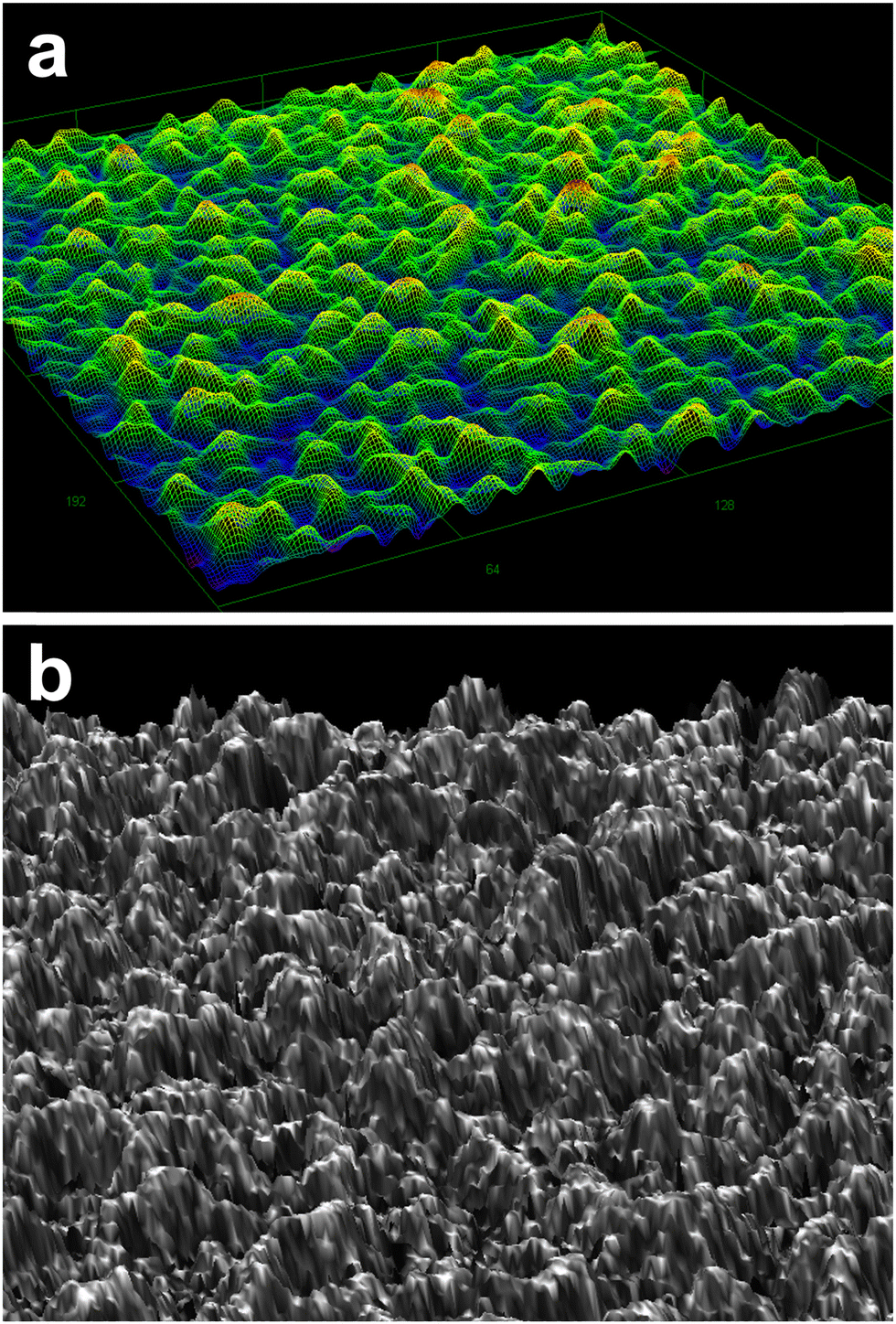 | ||
| Fig. 1 Bird's eye view images from a (a) differential interference contrast optical microscope, and (b) laser confocal imaging microscope. | ||
X-ray diffractions of (0002) and (0004) due to the GaN substrate are obvious in Fig. 2a. However, due to the extremely high intensity of the substrate other peaks are difficult to confirm. Therefore, the intensity of the XRD profile is plotted in the log scale in Fig. S3 (ESI†). Most XRD diffractions observed in Fig. S2 (ESI†) were assigned to the wurtzite CuGaO2; however, it is evident that some minor peaks related to Ga2O3 are also present due to the unreacted Ga2O3. The Rietveld analysis showed the molar fraction of CuGaO2: Ga2O3 = 86.1%: 13.9% on the surface of the GaN substrate. The digital photograph of the as-grown substrate is also shown in the inset. The brown color of the substrate suggests that the band gap of the film is smaller than 2 eV. It is noticed that the powder synthesized inside the crucible had a composition of CuGa2O4 with a spinel crystal structure, with a small amount of unreacted Ga2O3 as shown by star markers in Fig. S4 (ESI†). The BET surface area of the powder was 2.0592 m2 g−1. CuGa2O4 is also another interesting p-type material for photocatalytical properties; however, it is not clear why wurtzite CuGaO2 is grown on the GaN substrate, while spinel CuGa2O4 is synthesized in the powder form. One reason may be due to the fact that CuGa2O4 requires more oxidizing environment than CuGaO2 and the nucleation of CuGaO2 seeds is more probable to occur on the nitride substrate than the bulk. SEM micrographs of the CuGa2O4 powder are shown in Fig. S5 (ESI†).
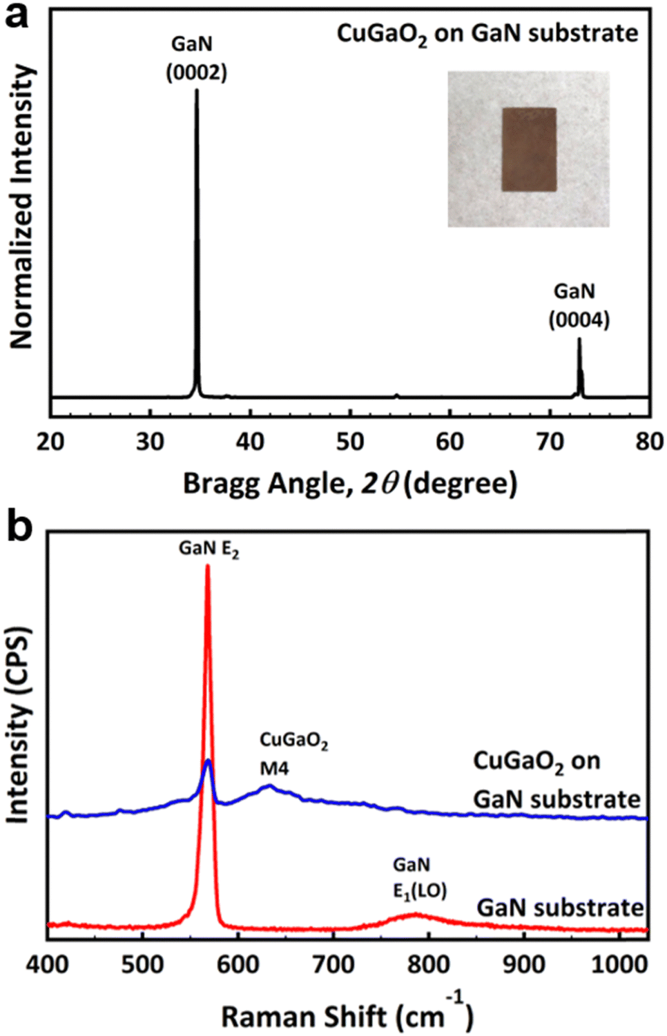 | ||
| Fig. 2 (a) XRD profile of a CuGaO2 film grown on the GaN substrate with a digital photograph of it in the inset, and (b) Raman spectra of the GaN substrate before and after epitaxial growth. | ||
The Raman profile of the GaN substrate shows typical c-plane GaN Raman modes of E2 at 568 cm−1, and A1(LO) at 786 cm−1. After the growth, however, the M4 Raman mode of CuGaO2 appeared at 635 nm−1 in addition to the Raman mode of the substrate, as shown in Fig. 2b.12 Considering the fact that the penetration depth of the 532 nm laser is less than 1 μm, the presence of GaN Raman peaks after growth means that the substrate is not fully covered by the film, or due to the morphology of the grains the penetration depth nominally gets larger as compared to the case if we had a uniform thickness structure. From the SEM cross-section image, it is confirmed that the thickness of the film on the substrate is about 10 μm, as shown by the green rectangle in Fig. 3a. The surface of the film observed by SEM is shown in Fig. 3b and corresponding EDS elemental mappings of Cu Kα, Ga Kα, and O Kα confirm the presence of each element on the film structure.
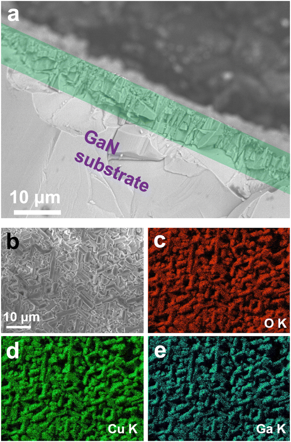 | ||
| Fig. 3 (a) SEM cross-section image of the film on the substrate, (b) SEM micrograph of the film surface, and EDS mapping of the corresponding elements (c) O Kα, (d) Cu Kα, and (e) O Kα. | ||
Fig. 4a shows the UV-Vis diffused reflectance spectra of the GaN substrate before and after growth. In both samples below a certain wavelength, known as the absorption edge, an intense absorption occurs. It is obvious that the absorption edge of the GaN substrate is 380 nm, while it shifts to the visible light region and reaches 670 nm after the growth of CuGaO2. No appreciable tail absorbance at wavelengths higher than the absorption edge is observed due to the existence of oxygen/copper vacancies or other types of defects that form localized states in the band gap. The absence of defects is beneficial for photocatalytic properties, leading to the longer lifetime of electron/hole carriers. Moreover, the high absorption intensity in both samples suggests that the electronic transition is direct. The band gap of the samples is estimated by Kubelka–Munk theory and summarized in Fig. 4b and c. The theory is based on eqn (1), where α is absorption coefficient, h is Planck's constant, and v is light frequency. n can take on values of 3, 2, 3/2, or 1/2, corresponding to indirect (forbidden), indirect (allowed), direct (forbidden), and direct (allowed) transitions, respectively. These plots of (αhν)nversus hν yield the value of the band gap when extrapolated to the baseline. The estimated band gaps are 3.40 eV and 1.84 eV for the GaN substrate and CuGaO2 on GaN, respectively. The estimated band gap for the GaN substrate is consistent with the reported values. The band gap of the sample after epitaxial growth was in good agreement with the reported value in the literature, 1.47 eV.8
| αhν = (hν − Eg)1/n | (1) |
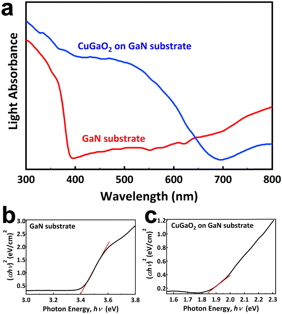 | ||
| Fig. 4 (a) UV-Vis diffused reflectance spectra of the GaN substrate and CuGa2O4 on GaN, and bandgap estimation of (b) the GaN substrate and (c) CuGaO2 on GaN samples. | ||
Photocatalytic water splitting hydrogen production test results are shown in Fig. 5a. It is shown that while the p-type powder has no activity under irradiation, the p–n heterostructure CuGaO2/GaN sample generates hydrogen under the presence of a hole scavenger sacrificial agent. The apparent quantum efficiency (AQE) measured under 380 nm monochromatic light also improved from 0% to 1.1% for the p–n heterostructure sample. Further studies are required for investigating the effect of the cocatalyst on the photocatalytic activity. Loading various types of cocatalysts such as Pt, RuO2, or Rh/Cr2O3 particles via the impregnation method can significantly improve the efficiency of the photocatalytic reaction. The stability of the CuGaO2/GaN sample was examined by cyclic photocatalytic test, as shown in Fig. 5b. It is shown that the amount of hydrogen production is reasonably similar for three cycles, indicating the potential of the p–n heterostructure for long-term photocatalytic activity. Moreover, the examination of the sample by XRD analysis before and after the photocatalysis test confirmed that the photocatalyst is stable under light irradiation, as shown in Fig. S6 (ESI†). The deposition of Pt cocatalysts on the surface of the film is confirmed to be successful, as shown in Fig. S7 (ESI†). Photocatalytic water splitting oxygen production test results are shown in Fig. 5c. It is evident that while p-type powder is effective for water splitting in the presence of Ag+ ions as an electron scavenger, the CuGaO2/GaN sample shows a six times higher oxygen generation rate. The higher rate of both hydrogen and oxygen generation for the CuGaO2/GaN sample with respect to the powder can be attributed to the effective charge separation of the electrons and holes in the proposed p–n heterostructure. The AQE was 2.9%, which is considered a relatively high efficiency. To compare CuGaO2/GaN with CuGaO2 instead of CuGa2O4 powder produced inside the crucible, we also synthesized the CuGaO2 by a hydrothermal method, as explained in the ESI.† The XRD profile shown in Fig. S8 (ESI†) is in good agreement with the hexagonal CuGaO2 with the space group of P63/mmc. As shown in Fig. S9 (ESI†), the photocatalytic hydrogen generation of the CuGaO2 was slightly better than that of CuGa2O4, both of which are much lower than the CuGaO2/GaN sample.
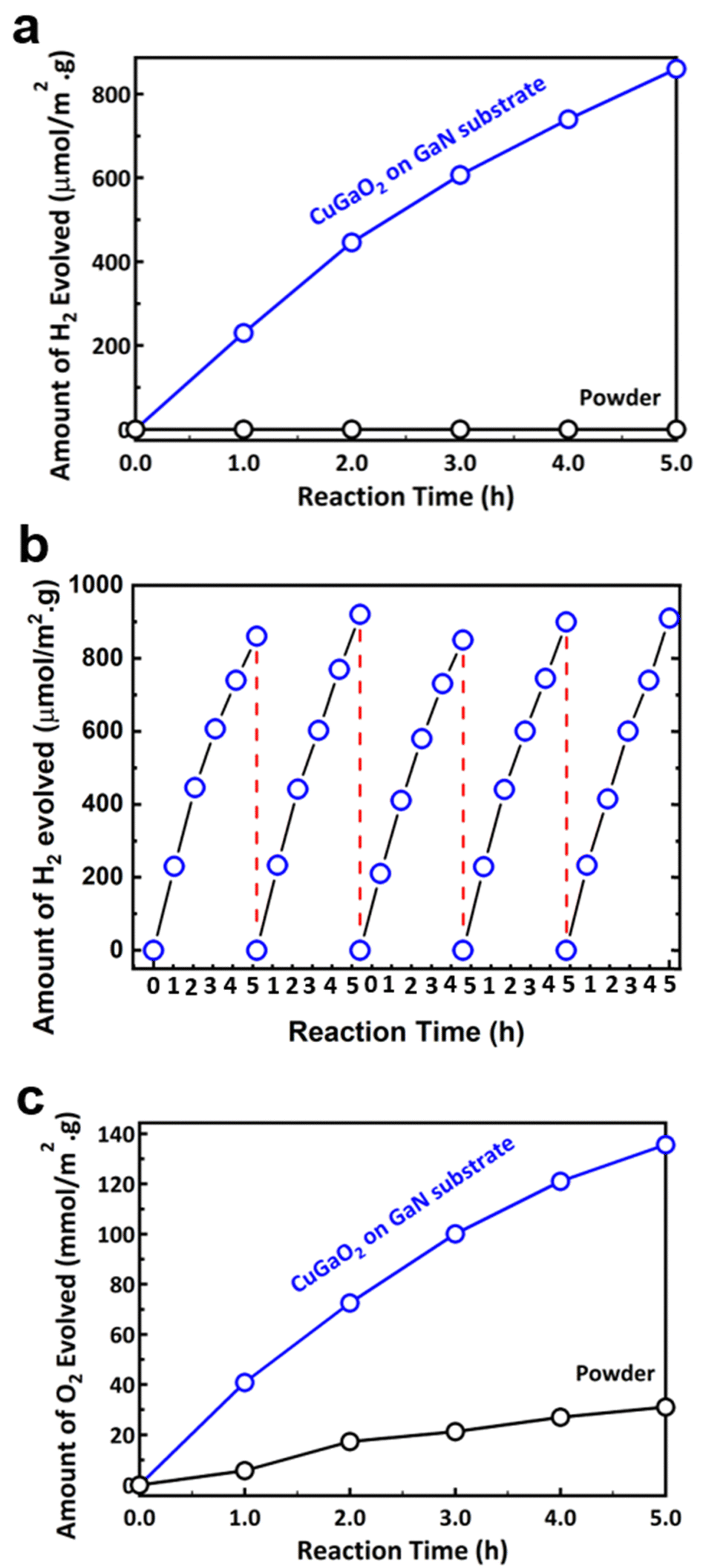 | ||
| Fig. 5 (a) Photocatalytic hydrogen generation of powder and CuGaO2 on GaN samples, (b) three cycles for the stability test of hydrogen generation of the CuGa2O4 on GaN sample, and (c) photocatalytic oxygen generation of powder and CuGaO2 on GaN samples. | ||
Fig. 6 shows the cathodoluminescence spectra of the GaN substrate and CuGaO2/GaN substrate. The sharp luminescence at 364.5 nm (3.4 eV) corresponds to the band gap of the GaN substrate. Its intensity is lower for the CuGaO2/GaN sample due to the efficient transfer of electrons from n-type GaN to the p-type CuGaO2 film. Less electron/hole recombination leads to a lower intensity of the CL. At the p–n junction and in equilibrium, electrons in the n-type GaN move to the p-side filling some of the holes in the p-type CuGaO2 due to the difference in Fermi levels of the two semiconductors. This causes an electric field at the junction. When irradiated with light, electrons will excite from the VB to the CB of each semiconductor, and because of the internal electric field, electrons will move from the CB of CuGaO2 to the CB of the GaN, and holes move from the VB of GaN to the VB of the CuGaO2. In this manner, the photogenerated electron–hole pairs are effectively separated by the p–n junction, and a high concentration of electrons is obtained in the CB of GaN, and a high concentration of holes is obtained in the VB of CuGaO2. The mechanism explains the effectiveness of the p–n heterostructure in charge separation of carriers; however, further studies are required for the calculation of the band structure of this p–n heterostructure. Also, we believe that this study, coupled with other well-known approaches like the Step-scheme (S-scheme), Z-scheme, and photoelectrochemical (PEC) approach, can open a new door for efficient photocatalyst development in the future.13–16
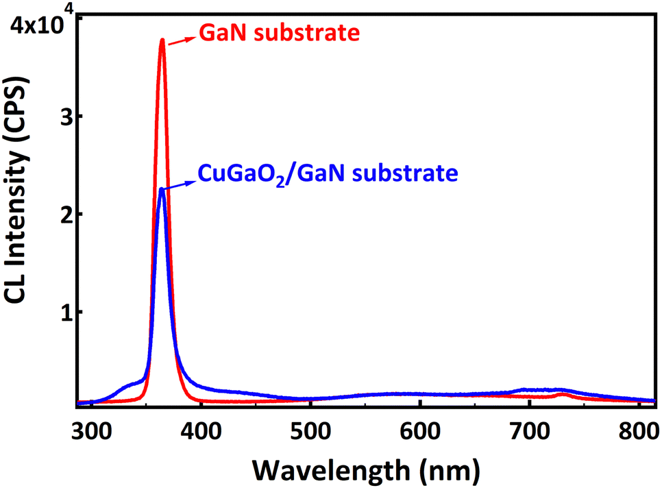 | ||
| Fig. 6 Cathodoluminescence spectra acquired for each sample. | ||
Conclusions
In summary, a p–n heterostructure of CuGaO2/GaN was designed for water-splitting reaction. The film was grown perpendicular to the GaN c-plane. The band gap was shown to be in the visible region, 1.84 eV. The water splitting reaction showed hydrogen generation of ∼800 μmol h−1 and oxygen generation of ∼120 mmol h−1. It was shown that the p–n heterostructure was effective for the charge separation of carriers for acquiring a high-efficiency photocatalyst.Author contributions
H. S.: investigation, data curation, visualization, writing, original draft preparation, supervision, reviewing and editing. S. K.: data curation, investigation, reviewing and editing. H. H.: reviewing and editing. M. F.: supervision, reviewing and editing. All authors contributed to the final version of this paper.Conflicts of interest
The authors declare no competing financial interests.Acknowledgements
This work was supported, in part, by JSPS KAKENHI Grant Number JP21K04138. We thank Sara Sena (Takasago Electric Inc.) for her contributions in synthesis and characterization.References
- A. J. Bard, Science, 1980, 207, 139–144 CrossRef CAS PubMed.
- K. Maeda, ACS Catal., 2013, 3, 1486–1503 CrossRef CAS.
- Y. Tachibana, L. Vayssieres and J. R. Durrant, Nat. Photonics, 2012, 6, 511–518 CrossRef CAS.
- M. G. Kibria, S. Zhao, F. A. Chowdhury, Q. Wang, H. P. T. Nguyen, M. L. Trudeau, H. Guo and Z. Mi, Nat. Commun., 2014, 5, 3825 CrossRef CAS PubMed.
- H. Razavi-Khosroshahi, K. Edalati, M. Hirayama, H. Emami, M. Arita, M. Yamauchi, H. Hagiwara, S. Ida, T. Ishihara, E. Akiba, Z. Horita and M. Fuji, ACS Catal., 2016, 6, 5103–5107 CrossRef CAS.
- H. Wang, L. Zhang, Z. Chen, J. Hu, S. Li, Z. Wang, J. Liu and X. Wang, Chem. Soc. Rev., 2014, 43, 5234–5244 RSC.
- H. Razavi-Khosroshahi, S. Mohammadzadeh, M. Hojamberdiev, S. Kitano, M. Yamauchi and M. Fuji, Adv. Powder Technol., 2019, 30, 1290–1296 CrossRef CAS.
- T. Omata, H. Nagatani, I. Suzuki, M. Kita, H. Yanagi and N. Ohashi, J. Am. Chem. Soc., 2014, 136, 3378–3381 CrossRef CAS PubMed.
- H. Zhang, H. Wang, W. Chen and A. K.-Y. Jen, Adv. Mater., 2017, 29, 1604984 CrossRef PubMed.
- A. R. C. Bredar, M. D. Blanchet, R. B. Comes and B. H. Farnum, ACS Appl. Energy Mater., 2019, 2, 19–28 CrossRef CAS.
- L. Chen, L. Qiu, L. Song, Y. Yuan, J. Xiong and P. Du, ACS Appl. Nano Mater., 2022, 5, 7312–7320 CrossRef CAS.
- M. Choi, C. Brabec and T. Hayakawa, Ceramics, 2022, 5, 655–672 CrossRef CAS.
- T.-M. Wang, Y.-X. Chen, M.-H. Tong, S.-W. Lin, J.-W. Zhou, X. Jiang and C.-Z. Lu, Chin. J. Struct. Chem., 2022, 41, 2202159–2202167 CAS.
- A. Meng, S. Zhou, D. Wen, P. Han and Y. Su, Chin. J. Catal., 2022, 43, 2548–2557 CrossRef CAS.
- W. Guo, H. Luo, Z. Jiang and W. Shangguan, Chin. J. Catal., 2022, 43, 316–328 CrossRef CAS.
- C. Yang, Y. Zhu, Y. Liu, H. Wang and D. Yang, J. Mater. Sci. Technol., 2022, 125, 59–66 CrossRef CAS.
Footnote |
| † Electronic supplementary information (ESI) available. See DOI: https://doi.org/10.1039/d3ya00226h |
| This journal is © The Royal Society of Chemistry 2023 |