
 Open Access Article
 This Open Access Article is licensed under a Creative Commons Attribution-Non Commercial 3.0 Unported Licence
Interfacial band alignment and photoelectrochemical properties of all-sputtered BiVO4/FeNiOx and BiVO4/FeMnOx p–n heterojunctions†
Andressa S.
Correa‡
a,
Lucas G.
Rabelo‡
 a,
Washington S.
Rosa
a,
Niqab
Khan
ab,
Satheesh
Krishnamurthy
c,
Sherdil
Khan
b and
Renato V.
Gonçalves
*a
a,
Washington S.
Rosa
a,
Niqab
Khan
ab,
Satheesh
Krishnamurthy
c,
Sherdil
Khan
b and
Renato V.
Gonçalves
*a
aSão Carlos Institute of Physics, University of São Paulo, PO Box 369, 13560-970 São Carlos, SP, Brazil. E-mail: rgoncalves@ifsc.usp.br
bLaboratory of Nanomaterials for Renewable Energy and Artificial Photosynthesis (NanoREAP), Federal University of Rio Grande do Sul (UFRGS), Campus do Vale, Agronomia, Porto Alegre-RS, Brazil
cSchool of Engineering and Innovation, The Open University, Milton Keynes, MK7 6AA, UK
First published on 28th November 2022
Abstract
BiVO4 is a well-known n-type semiconductor with great potential for photoelectrochemical (PEC) conversion of solar energy into chemical fuels. Nevertheless, photocurrent densities achieved for bare BiVO4 photoanodes are still far from their theoretical maximum due to the sluggish water oxidation kinetics and limitation in electron-hole recombination. In this work, magnetron sputtering deposition was used for depositing FeMOx (M = Ni, Mn) as cocatalyst layers to induce p–n heterojunctions and suppress charge recombination on BiVO4 photoanodes. The all-sputtered p–n heterojunction BiVO4/FeMnOx exhibited the highest photocurrent density (1.25 mA cm−2 at 1.23 V vs. RHE) and excellent chemical stability, indicating that the combination of Mn sites on Fe-based oxides provides promising cocatalytic materials for PEC applications. Experimental and theoretical techniques were used to investigate the interfacial band alignment and charge transport properties of BiVO4/FeMOx (M = Ni, Mn) heterojunctions. Our results show that type II heterojunctions arise in the BiVO4/FeMOx (M = Ni, Mn) interface after equilibrium, thereby providing potential barriers to inhibit electron flow from the BiVO4 to the FeMOx layers. Furthermore, the BiVO4/FeMnOx film showed a larger space charge region (SCR) characterized by a more intense built-in electric field than BiVO4/FeNiOx, explaining its higher PEC performance. In summary, this work provides a viable technique for producing photocatalytic heterojunction systems based on metal oxide semiconductors and introduces simple tools for investigating interface effects on photoinduced charge carrier pathways for PEC applications.
Introduction
Recently, photoelectrochemical (PEC) water splitting has attracted much attention due to its potential to provide a zero-emission pathway for hydrogen production. Typically, the PEC process involves an oxygen evolution reaction (OER) and a hydrogen evolution reaction (HER), which take place at the photoelectrode and counter electrode, respectively. The practical application of PEC is still challenging because of the availability of a suitable photoelectrode that can absorb a large portion of light, effectively separate charge, and have high surface reactivity. Among various developed photoanode materials, bismuth vanadate (BiVO4) has been widely regarded as a promising photoanode for converting solar energy into chemical fuels in photoelectrochemical (PEC) cells, showing visible light activity.1 The scheelite-monoclinic BiVO4 exhibits narrow bandgap energy (∼2.4–2.5 eV), with suitable band edge positions for water oxidation, earth-abundant composition, non-toxicity, and modest chemical stability in neutral electrolytes.2,3 Nevertheless, photocurrent densities measured for unmodified BiVO4 films are still significantly lower than the theoretical maximum value of 7.5 mA cm−2 (under AM 1.5G illumination) due to its fast electron-hole recombination and sluggish water reaction kinetics.4 As a result, several strategies have been employed to overcome these main limitations, including but not limited to doping with tungsten5 or molybdenum,6 depositing cocatalysts such as Co-Pi,7 FeCoOx,8 and FeNiOx,9 and forming anysotype heterojunctions.10,11Surface modification of BiVO4 films with metal oxide cocatalysts has been an essential strategy for accelerating the surface reaction kinetics and suppressing charge carrier recombination.12,13 Recently, iron-based bimetallic oxides have been established as low-cost and efficient cocatalysts for the oxygen evolution reaction (OER).8,9,14,15 For instance, Wang et al. synthesized BiVO4/FeCoOx films with an AM 1.5G photocurrent density of 4.82 mA cm−2 at +1.23 V vs. RHE and with excellent chemical stability.8 Similarly, Zhang et al. deposited FeNiOx cocatalyst onto boron-treated BiVO4 films, achieving a high photocurrent of 5.22 mA cm−2 at +1.23 V vs. RHE.9 X. Du et al. have also fabricated Fe0/MnOx/BiVO4 ternary magnetic assemblies using hydrothermal and photodeposition techniques that have shown a considerable increase in photocatalytic activity.16 Similarly, M sun et al. have developed manganese-based oxygen evolution catalysts, achieving a high current density of 4.85 mA cm−2 at +1.23 V vs. RHE.17 Besides the enhanced surface reaction kinetics, the heterojunction arising at the semiconductor/cocatalyst interface is essential to improve PEC performance. In particular, developing p–n heterojunctions has been widely applied for engineering the charge transport properties of semiconductor materials by inducing an interfacial built-in electric field that may assist in charge carrier separation and transport.18 Remarkably, charge separation efficiencies of about 90% have already been obtained after the deposition of p-type layers on the surface of bare BiVO4 films.8
Despite its recent efforts, most of the current PEC research examines an enhanced performance of heterojunctions utilizing flat band alignment diagrams derived from individual semiconductor information. This strategy completely ignores the interface effects that might occur during the formation of heterojunctions (i.e., band bending and built-in electric field) and provides no solid insights into charge transport properties in such materials, easily inducing misleading interpretations.19–21 Besides these, it remains uncertain how the interface affects the PEC activity of BiVO4-based heterojunctions, exemplified by inconsistent directions of charge flow as reported in several publications for BiVO4/WO3 films.21,22 These issues highlight the importance of establishing reliable tools for capturing interface effects on heterojunctions utilizing information from both individual semiconductors and heterostructured material. In this context, the X-ray Photoelectron Spectroscopy (XPS) technique has been widely employed to determine the valence band offset (through Kraut's method23) and built-in potentials of heterostructured systems,24,25 thereby directly determining its interfacial band alignment and charge transport properties.
Herein, motivated by the promise of BiVO4-based p–n heterojunctions for PEC applications and to answer the fundamental questions on interfaces, this work aims to provide a deep and comprehensive investigation of the influence of interfacial effects of BiVO4/FeMOx (M = Ni, Mn) heterojunctions on PEC water oxidation performance. To this end, we employed a well-established RF-magnetron sputtering technique to deposit n-type BiVO4 film from a homemade ceramic sputtering target and two p-type iron-based binary oxides {FeMOx (M = Ni, Mn)} cocatalysts for the first time to our knowledge. The interfacial band alignment and charge transport properties of BiVO4/FeNiOx and BiVO4/FeMnOx heterojunctions were examined using XPS spectroscopy, Mott–Schottky analysis, UV-vis spectroscopy, and the classical band bending model. Our results indicated that the BiVO4/FeMnOx interface produces a larger space charge region (SCR) than the BiVO4/FeNiOx, resulting in a more intense built-in electric field that readily accelerates the photogenerated charge carriers. This result is supported by the higher photocurrent densities and chemical stability of the BiVO4/FeMnOx heterojunction in PEC measurements. In summary, our study provides a viable technique for producing new heterojunction systems and illustrates how band energy alignment based on flat diagrams leads to misleading interpretations. In this work, we also introduce FeMnOx as a novel efficient cocatalyst for surface modification of n-type semiconductors applied to PEC water oxidation.
Experimental section
All chemicals were of analytical grade and were used as received without further purification. Fluorine-doped tin oxide (FTO) coated glass substrate with a surface resistivity of 7.0 Ω sq−1 was purchased from Sigma-Aldrich Ltda.Deposition of BiVO4 and bimetallic oxides FeMOx (M = Ni, Mn) films
RF-magnetron sputtering with a 2-inch homemade BiVO4 ceramic target was used to deposit BiVO4 (BVO) films on the surface of a cleaned FTO substrate at several deposition intervals (from 3 to 30 minutes). Details on the BiVO4 ceramic target fabrication can be found in the ESI.† All depositions were carried out at a constant operating distance of 5.0 cm between the targets and FTO substrates. Prior to the initial deposition of the BiVO4 target, a 30 minutes pre-sputtering deposition was performed to ensure that any potential contaminants on the surface of the target (such as adventitious carbon species) were removed. The base pressure and working pressure of the sputtering chamber for all deposition were set to 7.5 × 10⁻⁶ and 3.2 × 10⁻² Torr, respectively. The composition of the working pressure was a mixture of argon and oxygen gases (18.5 Ar scm and 2.1 O2 scm), and the RF power was set to 50 W for all deposition. After deposition, the BiVO4 film was annealed in an air atmosphere at 400 °C for 1 h, resulting in a crystalline film named BVO. Finally, a FeNiOx or FeMnOx thin layer was deposited over the BVO film using different metal alloy targets: FeMn (50 wt% Fe and 50 wt% Mn, 99.9% purity) and FeNi (50 wt% Fe and 50 wt% Ni, 99.9% purity), with an Ar/O2 (18.5![[thin space (1/6-em)]](https://www.rsc.org/images/entities/char_2009.gif) :2.1 scm) working pressure of 4.0 × 10⁻² torr and deposition times ranging from 30 to 120 seconds. Importantly, the deposition rate for the BiVO4 film was adjusted to 10.06 nm min−1, whereas the deposition rates for the FeNiOx and FeMnOx were 1.37 and 0.94 nm min−1, respectively.
:2.1 scm) working pressure of 4.0 × 10⁻² torr and deposition times ranging from 30 to 120 seconds. Importantly, the deposition rate for the BiVO4 film was adjusted to 10.06 nm min−1, whereas the deposition rates for the FeNiOx and FeMnOx were 1.37 and 0.94 nm min−1, respectively.
Characterization
X-ray diffraction (XRD) was used to investigate the structural properties of BiVO4 films (Rigaku Ultima IV diffractometer) with a Cu Kα radiation with 2θ angle from 10° to 80° and a step scan of 0.02°. Raman spectra were obtained using a WITec alpha 300 equipped with a linear stage, piezo-driven, objective lens Nikon 20× (NA = 0.46) and polarized laser with 514 nm wavelengths. Scanning electron microscopy (SEM) was used to investigate the morphology of the samples (Zeiss Sigma Gemini model field emission microscope operating at an accelerating voltage of 20 kV). The thicknesses of the BiVO4 and FeMOx (M = Ni, Mn) films were measured in a surface profilometer (Dektak 150, Veeco). UV-vis absorption measurements of the BiVO4 films were performed using a Shimadzu UV-2600 spectrometer fitted with an integrating sphere. Surface composition was analyzed by X-ray photoelectron spectroscopy (XPS) using a Scienta-Omicron ESCA+ spectrometer with a monochromatic Al Kα (hv = 1486.6 eV) radiation source. The XPS spectra were recorded at a pass energy of 30 eV with a 0.05 eV per step. Charging effects were eliminated using a low-energy electron flood gun. Adventitious carbon (C 1s) at 284.8 eV was used to calibrate the XPS spectra. Data analysis was performed using CasaXPS software using a Shirley-type background subtraction before the curve fitting. The high-resolution valence band XPS spectra were measured by linear extrapolation of the data to zero intensity, and the Fermi level of the sample corresponds to 0 eV on the binding energy axis (by definition).Photoelectrochemical measurements
Photoelectrochemical performance of photoanodes was carried out using a three-electrode configuration with the Autolab (PGSTAT128N) electrochemical workstation. The BVO-based thin films were used as a working electrode (area: 1 cm2), Ag/AgCl as the reference electrode and a platinum bar as the counter electrode. All PEC measurements were performed in a 1 M potassium borate buffer (KBi, pH 9.5). Before each PEC measurement, Ar gas was purged for at least 10 minutes to remove any dissolved oxygen. A solar simulator using a 300 W Xe lamp (ScienceTech, Inc.) coupled with an AM 1.5G filter at an intensity of 100 mW cm−2 was used as light source for all PEC measurements. The photocurrent density vs. applied potential curves was obtained using linear sweep voltammetry with a scan rate of 20 mV s−1. Electrochemical impedance spectroscopy (EIS) was performed with frequencies ranging from 0.1 Hz to 100 kHz at different voltages under constant illumination. The applied bias photon-to-current efficiency (ABPE) is calculated using the following equation: | (1) |
 | (2) |
The incident photon-to-current conversion efficiency (IPCE) was obtained using a Bausch&Lomb 1350 grooves/mm monochromator coupled with a 300 W Cermax Xe lamp as the simulated light source. In addition, an applied potential of 1.23 V vs. RHE was supplied by an Autolab workstation, and the power density at a specific wavelength was measured by a photometer Gentec XLP 12-3S-H2-D0. The IPCE values are calculated from equation (3), where j is the photocurrent density (mA cm−2), λ refers to the incident light wavelength (nm), and Plight is the power density obtained at a specific wavelength (mW cm−2).
 | (3) |
The estimated values of charge separation (ηsep(%)) and charge transfer (ηcat(%)) yields were calculated from the methodology proposed by Dotan. et al.30 In particular, the photocurrent densities observed in PEC measurements result from three distinct processes: (i) light absorption, (ii) separation and transport of photogenerated charges, and (iii) injection of photogenerated charges into the electrolyte. Therefore, the photocurrent density can be expressed by j = jabs × ηsep × ηinj where j (mA cm−2) is the current density observed in PEC measurements, jabs is the absorption current density defined as the photocurrent obtained when all absorbed photons are converted to electric current, ηsep is the electron-hole separation yield, and ηcat the charge carrier injection yield. The absorption current density (jabs) was calculated using the following equation:3
 | (4) |
Results and discussion
Synthesis, structural and optical properties of bare BVO and FeMOx (M = Co, Ni and Mn) films
RF-magnetron sputtering was employed to deposit BVO film from a homemade ceramic target. The thickness and annealing temperature parameters were varied to improve the crystallization and PEC performance of the as-prepared BiVO4 (BVO) films. Briefly, the film deposited for 8 minutes and calcined at 400 °C for 1 hour crystallizes in the desired BVO phase and has the highest PEC performance. Therefore, this optimized BVO film was employed for further characterizations and subsequent cocatalyst deposition. Fig. 1A shows the cross-sectional SEM image of bare BVO film after annealing at 400 °C for 1 h. The white shaded region of the SEM image represents the thickness of the FTO substrate, which is about 585 nm. If we closely look at the top of the FTO substrate in the SEM image, there is a thin layer of the BVO of ∼80 nm, which is consistent with its deposition rate of 10.06 nm min−1 (measured by profilometry). In addition, Fig. 1B exhibits the top-view SEM image of the bare BVO film, showing the presence of compact and uniform particles ranging from 30 to 50 nm, densely covering the surface of the FTO substrate, as expected from an RF-magnetron sputtering deposition. | ||
| Fig. 1 Characterization of bare BVO film deposited for 8 minutes and calcined at 400° for 1 hour: (A) cross-section SEM images, (B) Top view SEM images, (C) XRD patterns, (D) Raman spectrum and (E) UV-vis absorption spectrum, inset: Tauc Plot analysis. | ||
The crystalline structure of the bare BVO film was characterized using a combination of XRD and Raman spectroscopy. According to Fig. 1C, the prominent diffraction peaks observed in the XRD pattern corresponds to the monoclinic-scheelite (m-s) structure of BiVO4 (JCPDS Card No. 14-0688). The other additional peaks (represented with star sign) are all characteristic of the FTO substrate. Fig. 1D shows the Raman spectra of the bare BVO film, clearly evidencing five vibrational bands at about ∼210, 327, 367, 702, and 826 cm−1, which are typical signatures of monoclinic BiVO4. The more intense band at around 826 cm−1 corresponds to the symmetrical stretching mode of the V–O bonds, whereas the shoulder peak at 712 cm−1 is attributed to their asymmetric stretching modes. The vibration bands at ∼327 and 367 cm−1 are associated with asymmetric and symmetrical deformation modes of the VO4−3 tetrahedron, respectively. Finally, the band at ∼210 cm−1 is attributed to the external modes, corresponding to the translations and vibrations of the molecular entities within the crystalline structure.31,32
Diffuse UV-vis spectroscopy measurements were performed to investigate the optical properties of bare BVO film. Fig. 1E shows its absorption spectra, revealing a band edge absorption of ∼485 nm, which is typical of monoclinic BiVO4 with a bandgap energy of 2.4–2.6 eV. Remarkably, a broad and intense absorption tail is observed for wavelengths higher than 500 nm, indicating structural defects in the BVO film (confirmed by XPS analysis, as discussed below), which thereby result in localized states within the bandgap region.33 Furthermore, Tauc analysis of bare BVO film (inset of Fig. 1E) indicates a direct bandgap energy (considered due to the sharp increase in absorbance for lower wavelengths after the absorption onset) of about 2.60 eV, which is consistent with previous research.8,19,34
To suppress charge recombination and accelerate chemical reaction kinetics, we used the appropriate metal-alloy targets to deposit FeMOx (M = Ni, Mn) cocatalysts on the surface of BVO films. As shown in Fig. S2 (ESI†), Fe–Ni and Fe–Mn deposition for 60 seconds yield BVO/FeMOx heterojunctions with higher PEC performance. However, characterizing these heterostructured films becomes challenging due to the ultrathin thickness of the as-deposited FeMOx layers. Profilometry measurements estimated the thickness of FeMnOx and FeNiOx films to be 0.94 and 1.37 nm, respectively. In particular, there was no noticeable change in the XRD pattern or Raman spectrum of bare BVO after surface modification with FeNiOx and FeMnOx bimetallic oxides. As shown in Section 3.2, only XPS analysis can unambiguously confirm the presence of these cocatalysts on the surface of BVO films. Furthermore, determining the (photo)electrochemical properties of FeMOx layers is difficult for the same reasons mentioned above. As a result, we deposited FeMOx films on the FTO substrate with one hour of MSD (maintaining the other parameters) to extract their essential kinetic parameters (overpotentials) and band energy diagrams. The detailed deposition parameters, XRD patterns and Tauc plots of as-prepared FeMOx films are discussed in the ESI† (Fig. S3).
Electronic properties of bare BVO and BVO/FeMOx (M = Ni, Mn) films
X-ray photoelectron spectroscopy (XPS) was performed on the bare BVO and BVO/FeMOx (M = Ni, Mn) films to provide a comprehensive understanding of their electronic structure and surface chemical composition. Fig. 2A and B show the XPS spectra for bare BVO after annealing at 400 °C for 1 h. Highly resolved Bi 4f core-level spectra revealed two distinct peaks, with the Bi 4f5/2 peak at 164.2 eV and the Bi 4f7/2 peak at 158.9 eV. Both of these peaks are assigned to Bi3+ in the electronic structure of BiVO4, respectively.35 The high-resolution XPS spectra of the V 2p region display one spin–orbit doublet located at 516.6 eV and 524.3 eV, respectively. The spin–orbit split of 7.7 eV, which separates the V 2p3/2 and V 2p1/2 peaks, is typical for the V5+ oxidation state in the BiVO4 electronic structure. Nonetheless, the peak areas of the spin orbit split do not match the 2:1 ratio predicted for the 2p orbital. Furthermore, the line shape is asymmetric for a Gaussian/Lorentzian function, which might indicate the presence of another oxidation state, such as V4+, which could result in the formation of an oxygen defect/vacancy. In addition, the full width at half maximum (FWHM) for the V 2p1/2 peak is broadened than to the V 2p3/2, where the ratio of FWHM for these two peaks was 1.62 eV, attributable to the Coster–Kronig effect, where distinguishing V5+ and V4+ species by XPS is a challenging operation to identify them precisely.36,37
 | ||
| Fig. 2 XPS spectra of bare BiVO4 at 400 °C for 1 hour: (A) Bi 4f and (B) V 2p. XPS spectra of as-sputtered FeMOx (M = Ni, Mn) on BVO films: (C) Fe 2p with FeNiOx deposited for 60 s, (D) Fe 2p with FeMnOx deposited for 60 s, (E) Ni 2p with FeNiOx deposited for 60 s, and (F) Mn 2p with FeMnOx deposited for 60 s. | ||
Furthermore, Fig. S4 (ESI†) shows that the O 1s XPS spectra for the bare BVO film can be fitted into three distinct peaks. The peak observed at 529.5 eV corresponded to oxygen lattice in BiVO4, while the peak at 531.3 eV is commonly attributed to signals from oxygen defects in a semiconductor structure, associated with oxygen vacancies, and the less intense peak observed at 532.7 eV is associated with C–O groups.8,38 The presence of oxygen vacancy/defects (Ovo) can significantly modify the electronic structure of BiVO4 and, hence photoelectrochemical characteristics of the compound. Several studies have proposed that the oxygen vacancies may induce charge transition levels within the bandgap (intragap), resulting in a reduction in the recombination site and an increase in n-type conductivity, which are responsible for the increased photocatalytic activity of BiVO4.39 As previously noted, the existence of oxygen vacancies/defects is a significant indicator of V5+/V4+ in the electronic structure of BVO. Beyond oxygen vacancies/defects, adjusting the atomic ratio of Bi/V in the structure of BiVO4 through a solution containing vanadium ions has been an essential strategy to improve PEC performance in the water splitting reaction.39
XPS was also used to characterize the chemical surface composition of the as-deposited FeMOx (M = Ni, Mn) layers through RF-magnetron sputtering on the surface of BVO films. The Fe 2p XPS spectra of FeNiOx and FeMnOx are shown in Fig. 2C and D. All high-resolution spectra of Fe 2p presented a spin–orbit doublet located close to 711.2 eV and 724.9 eV, which corresponds to the spin–orbital splitting of 2p3/2 and 2p1/2 of Fe3+ ions in the FeNiOx and FeMnOx structures.40,41 The XPS spectra of Ni 2p (Fig. 2E) show two characteristic peaks at 855.6 and 873.2 eV, corresponding to the Ni2+ oxidation state. In addition, the presence of two more intense satellite peaks around 861.3 and 879.3 eV may also indicate the presence of Ni2+ in the FeNiOx structure. Finally, the Mn 2p spectra (Fig. 2F) can be deconvoluted into four peaks using an asymmetric Gaussian–Lorentzian function with a ratio G:L (60:40). The peaks at 653.8 and 641.7 eV can be attributed to the Mn3+ species, while the two other peaks at 652.4 and 640.5 eV correspond to the binding energy of Mn2+. It has been noticed that the doublet separation of both Mn3+ and Mn2+ species for Mn 2p is 12.1 eV, which is slightly higher than that of the Mn oxide bulk material commonly reported in the literature, which has a spin–orbit separation of between 11.0 and 12.0 eV.40 As a result of the small size of the FeMnOx cocatalyst that was deposited on the BVO surface by magnetron sputtering, it is possible that there is a strong interaction between Mn–Fe–O atoms and the BVO layer, which could explain the slight displacement.
Photoelectrochemical properties of bare BVO and BVO/FeMOx (M = Ni, Mn) films
The PEC performance of bare BVO and BVO/FeMOx (M = Ni, Mn) films wares evaluated in a 1 M potassium borate buffer (KBi, pH 9.5). Fig. 3A shows the current density vs. applied potential (j–V) curves under constant 100 mW cm−2 AM 1.5G illumination. The bare BVO film exhibits an onset potential of around 0.47 V vs. RHE and a photocurrent density of only 0.50 mA cm−2 at the water oxidation potential (+1.23 V vs. RHE). This photocurrent density is comparable to that obtained for bare BVO films deposited via MSD,19,39 but much lower than those obtained from electrodeposition technique.8,9 Encouragingly, all surface-modified BVO films showed significantly enhanced PEC performance, with the new BVO/FeMnOx photoanode achieving the highest photocurrent density of 1.25 mA cm−2 at +1.23 V vs. RHE. Moreover, upon FeMnOx deposition, the onset potential of bare BVO was cathodic shifted to +0.33 V vs. RHE (corresponding to a ≈ 140 mV shift), indicating improved charge separation efficiency in the low applied potential range. Interestingly, the BVO/FeNiOx heterojunction exhibited a similar onset potential at around 0.34 V vs. RHE but a significantly lower photocurrent density of 1.00 mA cm−2 at +1.23 V vs. RHE compared with the BVO/FeMnOx film. To further investigate the enhanced PEC performance of the surface-modified BVO films, the applied bias photon-to-current efficiency (ABPE) curves of the BVO, BVO/FeNiOx, and BVO/FeMnOx films were determined using equation (1). As shown in Fig. 3B, the bare BVO film exhibits an ABPE peak of only 0.04% at around 1.01 V vs. RHE, whereas the ABPE peak of the BVO/FeNiOx reaches a significant increase of 0.26% at a lower potential (0.79 V vs. RHE). In contrast, the FeMnOx cocatalyst further improves the optimal ABPE to 0.39% (at 0.74 V vs. RHE), which is almost tenfold higher than the bare BVO film. These results indicate that surface modification of the BVO top layer with an OER cocatalyst is essential for solving its intrinsic sluggish water oxidation kinetics and surface charge recombination. Crucially, the j–V and ABPE curves clearly prove that the FeMnOx compound has superior catalytic activity for the PEC water oxidation than the conventional FeNiOx cocatalyst.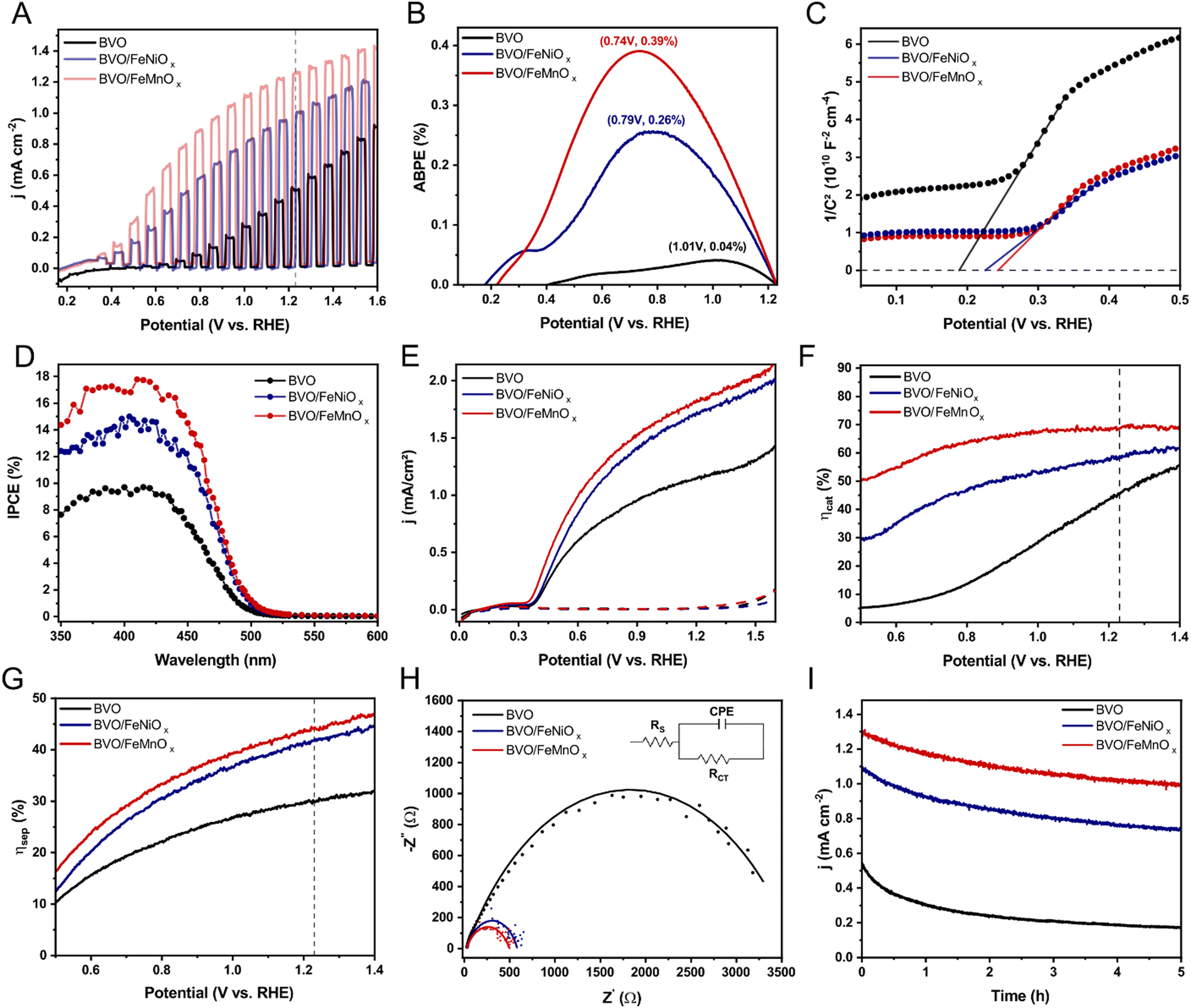 | ||
| Fig. 3 Photoelectrochemical properties of BVO-based photoanodes: (A) photocurrent density vs. applied potential curves with 1 M KBi (pH 9.5); (B) ABPE curves; (C) Mott–Schottky curves; (D) IPCE curves obtained at +1.23 V vs. RHE; (E) photocurrent density vs. applied potential curves with 0.25 M Na2SO3 as a hole scavenger; (F) charge transfer efficiencies and (G) charge separation efficiency at different applied potentials; (H) EIS response measured under +0.90 V vs. RHE and (inset) the equivalent circuit model (RS, RCT and CPE refers to series resistance, charge transfer resistance and the constant phase element, respectively); (I) temporal stability by chronoamperometry measurements of bare BVO and BVO/FeMOx (M = Ni, Mn) heterojunctions. | ||
It is well-known that the formation of p–n heterojunctions considerably enhances the charge separation due to a built-in electric field, which accelerates photogenerated charges and outperforms the negative effects of electrical resistance and recombination centers at the BVO/p-type layer interface.11,19,42 As will be shown in Section 3.4, the FeNiOx and FeMnOx layers unambiguously exhibit p-type character. Therefore, to verify the possible development of p–n heterojunctions in our surface-modified BVO films, Mott–Schottky curves of bare BVO, BVO/FeNiOx, and BVO/FeMnOx films were measured at 1 kHz under dark conditions. Fig. 3C indicates that all heterojunctions show a positive shift in the flat band potential compared to bare BVO, evidencing that Fermi energy shifts once the bimetallic oxides contact the BVO surface. Consequently, the Fermi energy of the BVO is shifted to higher energies after contact with FeNiOx and FeMnOx layers, unambiguously demonstrating the development of p–n heterojunctions.8,19 Remarkably, the electron concentrations (ND) in the bare BVO and BVO/FeMOx (M = Ni, Mn) heterojunctions – determined from the slopes of the straight lines shown in Fig. 3C – are around 1019 cm−3 for all films, indicating that there is no apparent increase in ND of bare BVO film after the formation of the p–n heterojunctions, which is most likely due to the ultrathin thickness of the bimetallic oxide layers deposited on the surface of BVO film.
To investigate the influence of light absorption on enhanced PEC performance of the surface-modified BVO films, we measured their incident-photon-to-current (IPCE) values under monochromatic illumination of different wavelengths and subjected to +1.23 V vs. RHE. As shown in Fig. 3D, the BVO/FeNiOx and BVO/FeMnOx photoanodes have higher IPCE values for all measured wavelengths, evidencing the enhanced optical properties upon the deposition of bimetallic oxide cocatalysts on the BVO surface. The bare BVO film, in particular, exhibits an absorption threshold potential close to 495 eV, which is consistent with UV-Vis spectra; additionally, the conversion of photons with energy less than 2.5 eV (>495 nm) into the electrical current is null (IPCE ≈ 0), indicating that the tail absorption band observed in Fig. 1E plays no direct role in the PEC performance of bare BVO film. Interestingly, all BVO/FeMOx heterojunctions (M = Ni, Mn) have identical potential absorption thresholds with a red shift compared to bare BVO film (corroborating with UV-Vis analysis, see Fig. S5, ESI†), suggesting that a higher number of photons may be efficiently converted to electrical current. Significantly, the IPCE values at 400 nm, as an example, increase to 14.4% for BVO/FeNiOx and 16.9% for BVO/FeMnOx compared to 9.6% for bare BVO film. Similarly, since IPCE values beyond the threshold potential are null, the extended absorption tail bands seen in Fig. S5 (ESI†) for all BVO/FeMOx (M = Ni, Mn) heterojunctions cannot be directly converted to photocurrent densities.
To unravel the charge-separation effect across the BVO/FeMOx (M = Ni, Mn) p–n heterojunctions, the photocurrent density (j) from the PEC measurements was decoupled into three significant contributions: j = jabs × ηcat × ηsep, as detailed in the experimental section.30 The values of jabs for bare BVO, BVO/FeNiOx, and BVO/FeMnOx heterojunctions, calculated from equation (4), are 3.86, 4.15, and 4.17 mA cm−2, respectively (Fig. S6, ESI†). To assess the charge separation (ηsep) and interfacial transfer efficiencies (ηcat), we performed the PEC measurements with 1 M KBi in the presence of 0.25 M Na2SO3. As shown in Fig. 3E, the Na2SO3 species exhibits fast kinetics for consuming photogenerated holes at the semiconductor-electrolyte interface (ηcat ∼ 1 and ηsep ≈ j/jabs), resulting in higher photocurrent density values. Fig. 3F and G show the calculated efficiencies as a function of the applied potential. For the bare BVO photoanode, both ηcat and ηsep rise from small values under low applied potentials to ∼45.0 and ∼29.9%, respectively, at +1.23 V vs. RHE. As a result, the charge separation effect is the key-liming factor during the PEC water oxidation with BVO films, indicating that surface modification techniques are essential. Conclusively, the BVO/FeMnOx photoanode significantly enhances the charge separation efficiency under low applied bias, reaching ∼44.3% at +1.23 V vs. RHE. Moreover, the catalytic efficiency was also dramatically improved, reaching 68.7% at +1.23 V vs. RHE. Interestingly, the BVO/FeNiOx exhibits a similar charge separation efficiency of ∼41.8% at +1.23 V vs. RHE compared with the BVO/FeMnOx, but a significantly lower catalytic efficiency of 58.8% at the same potential. These significant results indicate that the FeMnOx has superior activity (compared to conventional FeNiOx) for separating photogenerated charges (due to the presence of a more intense built-in electric field, as will be discussed in Section 3.4) and consuming the photogenerated holes from the BVO layer, thereby reducing the onset potential for water oxidation and enhancing the PEC performance, which is consistent with Fig. 3A.
To further investigate the interfacial charge transfer kinetics at the photoanode/electrolyte interfaces, we performed electrochemical impedance spectroscopy (EIS) curves of BVO, BVO/FeNiOx, and BVO/FeMnOx photoanodes at +0.90 V vs. RHE under constant 100 mW cm−2 AM 1.5G illumination. As shown in Fig. 3H, the Nyquist plots of bare BVO and BVO/FeMOx (M = Ni, Mn) heterojunctions exhibit only a single semicircle, which can be simulated from the equivalent circuit shown in the onset, characterized by a series resistance (RS) through the material, charge transfer resistance (Rct) at the photoanode/electrolyte interface and a constant phase element (CPE) to describe the double-layer capacitance across the inhomogeneous electrode surface.43 The diameters of the Nyquist semicircles give information about RCT, thereby providing a direct comparison between electron transfer kinetics at the photoanode/electrolyte interface for different films. According to Table S1 (ESI†), the calculated Rct values for BVO/FeMOx (M = Ni, Mn) heterostructures are significantly lower than that of bare BVO, clearly indicating that the synergetic effect of heterojunction formation and cocatalyst effect may improve interfacial charge separation and increase the overall PEC performance. Interestingly, the new BVO/FeMnOx film exhibited the lowest Rct value, indicating that the FeMnOx layer has superior cocatalyst activity compared with conventional FeNiOx, corroborating the higher ηcat efficiency and photocurrent density values.
The PEC stability of bare BVO, BVO/FeNiOx, and BVO/FeMnOx photoanodes were evaluated through chronoamperometry measurements (j–t curves). Fig. 3I shows the j–t curves for the BVO-based photoanodes submitted to 1.23 V vs. RHE and under AM 1.5G illumination for 5 hours. The bare BVO film, in particular, exhibits severe instability in the 1 M KBi buffer at pH 9.5, retaining only 31.7% of its initial value during 5 hours. The chemical instability of BVO photoanodes in the presence of potassium borate species at pH 9.5 is probably attributed to significant photo corrosion of the BVO layer during the PEC measurement. In contrast, the BVO/FeNiOx and BVO/FeMnOx films exhibit superior PEC stability, retaining ∼67.7% and ∼77.2% of their initial photocurrent density during 5 hours, respectively. These significant results indicate that the deposition of Fe-based bimetallic oxides also protects the BVO layer from photocorrosion, consistent with previous research concerning BVO/FeCoOx heterojunctions.8,19 To further compare the effect of the different bimetallic oxides for improving the PEC performance of the BVO film, we determined the electrochemical kinetic parameters and energy band alignment (discussed in Section 3.4) of the bare FeNiOx and FeMnOx films. Importantly, these films were deposited on FTO substrates using one hour of MSD, keeping the other parameters for preparing the BVO/FeMOx (M = Ni, Mn) photoanodes. Current density versus applied potential (j–V) curves was measured under dark conditions to access the overpotential of FeMOx (M = Ni, Mn) films. As shown in Fig. S7 (ESI†), the FeMnOx film exhibits a smaller overpotential to reach 10 mA cm−2 (η = 875 mV) compared to FeNiOx (η = 922 mV) and a steeper water oxidation current density, resulting in a higher surface water oxidation kinetics and clearly justifying the superior OER catalytic performance of the FeMnOx compound compared to conventional FeNiOx.
Interfacial band alignment of BVO/FeMOx (M = Ni, Mn) heterojunctions
To provide solid insights into the interfacial band alignment and charge transfer process in the BVO-based heterojunctions, we begin by constructing the semiconductor band diagrams from UV-Vis spectroscopy, valence band (VB) XPS spectra, and Mott–Schottky analysis. Fig. 4A shows the VB XPS spectra of bare BVO and bare FeMOx (M = Ni, Mn) films, indicating the distance between the Fermi energy (EF) and the VB maximum (EV) as the intersection of the baseline intensity and the linear extrapolation of the leading edge of VB.19,44,45 The BVO film has a VB maximum located 1.72 eV below the Fermi level, indicating its n-type nature. In contrast, the bimetallic oxide films exhibit a VB edge with only 0.60 and 0.68 eV below EF for FeNiOx and FeMnOx films, respectively, evidencing their p-type nature. Furthermore, Mott–Schottky curves of the bare BVO and bare FeMOx (M = Ni, Mn) films were performed at 1 kHz under the dark condition to estimate their Fermi energy position and dopant concentrations. As shown in Fig. 4B, the BVO film exhibits a straight line with a positive slope, characteristic of n-type semiconductors, resulting in a flat band potential (EFb) of 0.19 V vs. RHE and an electron concentration (ND) of 6.6 × 1018 cm−3. Conversely, all bimetallic oxides show a straight line with a negative slope, confirming their p-type nature. The FeNiOx has a flat band potential at around 0.96 V vs. RHE and acceptor concentration (NA) of 3.6 × 1021 cm−3, whereas the FeMnOx film exhibits a flat band potential at 1.13 V vs. RHE and a high acceptor concentration of 3.3 × 1022 cm−3. The band diagrams sketched in Fig. 4C are derived by assuming EFB ≈ EF (considering isolated semiconductors) and combining the VB measured by XPS, Mott–Schottky analysis, and bandgap energies obtained from the UV-Vis spectroscopy (Fig. 1E and Fig. S3, ESI†), as reported elsewhere.19,46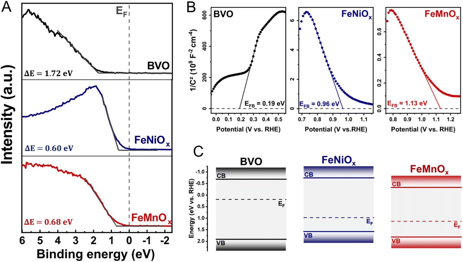 | ||
| Fig. 4 (A) valence band XPS spectra for bare BVO and bare FeMOx films; (B) Mott Schottky plot for bare BVO and bare FeMOx films; (C) band diagrams for isolated BVO and FeMOx semiconductors. (M = Ni, Mn). In Fig. 4A, ΔE indicates the distance between the valence band edge (EV) and Fermi level energy: ΔE = EV − EF. | ||
According to the traditional band alignment based on flat band diagrams, the BVO/FeMnOx heterojunction exhibits a typical type I alignment (see Fig. S8, ESI†), where photogenerated holes in the VB of the BVO layer tend to migrate towards the VB of FeMnOx cocatalyst, and photogenerated electrons in the CB of BVO tend to flow into the CB of FeMnOx. However, the photogenerated electrons in the BVO layer must travel to the FTO substrate to conduct the reduction reactions. Therefore, the electron transfer from BVO to the FeMnOx side potentially limits the PEC performance of the BVO/FeMnOx heterojunction, which clearly contradicts the results of Section 3.3. Similarly, although the BVO/FeNiOx heterojunction presents a typical type II alignment, there is no obvious mechanism that prevents the transfer of electrons from FeNiOx to the BVO layer due to its staggered conduction bands (at room temperature, kT/e ≈ 26 meV, the electrons may eventually tunnel through the potential barrier ΔEC = 60 meV). In conclusion, the absence of type II heterojunctions with high values of conduction band offsets (ΔEC) suggests the existence of p–n heterojunctions with limited PEC performance because they lack adequate potential barriers to prevent the flow of photogenerated electrons from BVO to FeMOx layer. However, as pointed out recently in several publications,19–21 the interfacial alignment using flat band diagrams may lead to misleading interpretations because it ignores the physical effects that occur at the interface during the heterojunction formation, as discussed below.
From the classical band theory, immediately after contact, there is a preferential flow of electrons from FeMOx (semiconductor with higher EF) to BVO (with lower EF) layer to produce a constant Fermi level throughout the entire material (representing a net zero current flow through the p–n heterojunction).18–20 Consequently, (i) the FeMOx valence and conduction bands tend to increase in energy along with its Fermi level, while the valence and conduction bands of the BVO tend to decrease following its Fermi level, and (ii) the band bending effect occurs at the interface between the semiconductors, which is characterized by the development of a built-in electric field that can mediate the separation and transfer of photoinduced charges. Fig. 5A and B depict the interfacial band alignment of the BVO/FeMOx (M = Ni, Mn) heterojunctions constructed from the classical band bending model (details are available in ESI†) under equilibrium conditions, clearly capturing the consequences (i) and (ii) mentioned above. From this result, each p–n interface has a distinct space charge region (SCR) that is defined by the energy drops Ψn and Ψp supported in the n and p layers, respectively, the depletion lengths Wn and Wp in the corresponding layers (whose values are shown in Table 1), and the built-in electric field that points from the n to the p side. Importantly, this built-in electric field accelerates the photogenerated electrons in the CB of the BVO layer to the FTO substrate, providing a mechanism that tends to inhibit the flow of electrons to the FeMOx layer. Interestingly, both BVO/FeNiOx and FeMnOx heterojunctions have a space charge region entirely concentrated on the BVO side, resulting from the higher impurity concentration values in the bimetallic oxides (NA ≫ ND). Furthermore, Table 1 shows that the BVO/FeMnOx heterojunction display a larger SCR both in spatial (Wn) and energetic extent (Ψn) compared to BVO/FeNiOx, suggesting the formation of a more intense built-in electric field that may effectively decrease the onset potential and increase the photocurrent density, which is consistent with the PEC measurements.
 | ||
| Fig. 5 Interfacial band alignment obtained from the classical band model under dark conditions for (A) BVO/FeNiOx and (B) BVO/FeMnOx films. High-resolution XPS (C) V 2p3/2 and Bi 4f7/2 spectra for bare BVO and BVO/FeMOx (M = Ni, Mn) heterojunctions, and high-resolution XPS (D) M 2p3/2 (M = Ni, Mn) for bare FeMOx films and the corresponding BVO/FeMOx heterojunctions. | ||
| Heterojunction | Ψ n (meV) | Ψ p (meV) | Wn (nm) | Wp (nm) | E F (eV) |
|---|---|---|---|---|---|
| BiVO4/FeNiOx | 772 | 7.44 | 29.65 | 0.05 | 0.96 |
| BiVO4/FeMnOx | 940 | 0.72 | 32.70 | 0.01 | 1.13 |
The classical analysis of band bending is performed with a band diagram under the equilibrium condition, without applied light and external bias. It is well-known that the band flattening effect occurs upon AM 1.5G illumination and forward external bias. This effect is characterized by: (i) a reduction in the spatial and energetic extension of SCR, resulting in a decrease of built-in electric field intensity, and (ii) the splitting of constant Fermi levels into quasi-Fermi levels for holes and electrons.20 As a result, the built-in electric field considerably weakens during PEC measurements, potentially allowing photogenerated electrons in the CB of the BVO to migrate into the FeMOx layer (see Fig. S9, ESI†). Therefore, these results (contradicting the PEC measurements) suggest that the electron affinity law, used as a hypothesis in the band bending model, is not respected in the BVO/FeMOx heterojunctions.18 To solve this problem, we employed Kraut's method to directly determine the interfacial band alignment of our p–n heterojunctions from the XPS technique.
Kraut's method, in particular, directly determines the VB offsets (ΔEV) from the relative displacement of the binding energies (BE) of some core levels (and the values of the VB maximum) between the individual semiconductor films and the corresponding heterojunctions.23 To apply this method, we investigated the XPS core-level spectra of bare BVO, bare FeMOx (M = Ni, Mn), and the heterostructured films (BVO/FeNiOx and BVO/FeMnOx). Fig. 5C displays the XPS high-resolution spectra of Bi 4f7/2 for the BVO film and the BVO/FeMOx heterojunctions. This result shows that the deposition of bimetallic oxides causes a relative decrease in the BE of Bi 4f7/2 core levels, which is a characteristic signature of the upward band bending effect, as expected when forming the p–n heterojunction.24,47Fig. 5D shows the high-resolution XPS spectra for Ni 2p3/2 and Mn 2p3/2 for the bare FeMOx films and the subsequent BVO/FeMOx heterojunctions. As indicated in Fig. S11 (ESI†) and Table 2, the predominant peak center (referring to Ni2+ for BVO/FeNiOx and Mn3+ for BVO/FeMnOx) was considered as the core-level peak position. Importantly, the peak at 642 eV in the BVO/FeMnOx heterojunction and the lack of the peak centered at 854 eV for the bare FeNiOx film are likely the results of the strong interaction between the bimetallic oxide atoms and the BVO layer. Crucially, the slight shifts of the core-level peak position of FeNiOx and FeMnOx to the higher BE (compared to the heterostructured films) are directly related to the downward band bending on the p-side of the heterojunction, also indicating the formation of a p–n heterojunction.48 Based on these core-level peak shifts, the VB offset can be calculated from Kraut's equation:
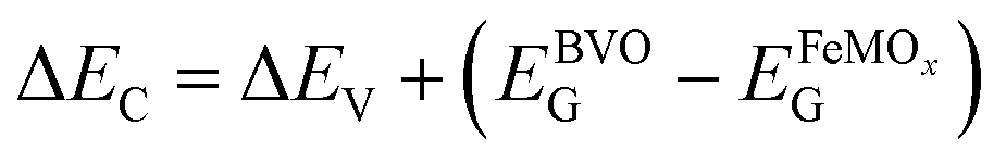
| ΔEV= (EM2p − EVBM)FeMOx − (EBi4f − EVBM)BVO + (EBi4f − EM2p)BVO/FeMOx, | (5) |
 , where EBVOG and
  are the bandgap energies of BVO and FeMOx bare films. Table 2 exhibits the ΔEV and ΔEC values for the BVO/FeMOx films calculated from the equations above.
| Film | E(Co 2p) | E(Ni 2p) | E(Mn 2p) | E(Bi 4f) | E(V 2p) | E V | ΔEV | ΔEC |
|---|---|---|---|---|---|---|---|---|
| BiVO4 | 158.92 | 516.72 | 1.72 | |||||
| FeNiOx | 855.59 | 0.60 | ||||||
| FeMnOx | 641.67 | 0.68 | ||||||
| BVO/FeNiOx | 855.60 | 158.81 | 516.61 | 1.00 | 0.72 | |||
| BVO/FeMnOx | 641.78 | 158.79 | 516.58 | 0.80 | 0.35 |
Fig. 6A and B shows the interfacial band alignment of the BVO/FeMOx (M = Ni, Mn) heterojunctions under dark conditions, considering the ΔEC and ΔEV values calculated by the Kraut's method and the energy drops (Ψn and Ψp) and depletion lengths (Wn and Wp) determined from classic band bending model. Since the values of ΔEV and ΔEC are both positive, typical type II heterojunctions are formed at the BVO/FeMOx interfaces. Importantly, this configuration is ideal for enhancing the PEC performance of photoanodes because the photogenerated holes in the VB of the BVO layer are readily transported to the VB of the FeMOx layer, and the corresponding photogenerated electrons are effectively maintained in the CB of the BVO. Furthermore, the p–n heterojunction induces a built-in electric field, which assists in the transport and separation of the photogenerated charges at the heterojunction, accelerating the holes towards the FeMOx layer and the electrons towards the FTO substrate. Fig. 6C and D show the qualitative interfacial band alignment of BVO/FeMOx heterojunctions (corrected with Kraut's method) under AM 1.5G illumination, clearly indicating the band flattening effect. In this case, although the built-in electric field is considerably weakened, the ΔENiC and ΔEMnC potential barriers inhibit the flow of electrons from the CB of the BVO to the CB of the FeMOx layer (since ΔENi,MnC/e ≫ kT/e at room temperature), ensuring that these electrons are transported to the FTO substrate. Conclusively, our results show that the BVO/FeMnOx heterojunction presents a more intense built-in electric field (indicated by a large SCR) than the BVO/FeNiOx photoanode, suggesting a superior PEC performance which is confirmed by our PEC experiments.
 | ||
| Fig. 6 Interfacial band alignment obtained from Kraut's method combined with the classical band model under dark conditions for (A) BVO/FeNiOx and (B) BVO/FeMnOx films, and under AM 1.5 illumination for (C) BVO/FeNiOx, and (D) BVO/FeMnOx films. Notice that due to band flattening effect, the energy drops and lengths upon illumination (ΦMn and ωMn) are significantly lower than that under dark conditions (ΨMn and WMn), where M = Ni, Mn. | ||
In summary, the simulated interfacial band alignment of our p–n heterojunctions (with or without illumination) show that the deposition of FeMOx (M = Ni, Mn) ultrathin layers can induce significant bending of the BVO energy bands, indicating that in addition to acting as efficient cocatalysts – reducing overpotential for the water oxidation reaction and considerably lowering the resistance at the photoanode/electrolyte interface – they also promote enhanced separation and transport of charges due to the induction of local p–n heterojunctions on the surface of BVO. Interestingly, we showed that the interfacial band alignment using flat diagrams before equilibrium produces misleading results, contradicting the evaluated PEC performance of our photoanodes. In contrast, the combination of Kraut's method with the classical band bending model clearly demonstrates the formation of type II heterojunctions at the BVO/FeMOx interface, also indicating the presence of a built-in electric field that accelerates the photogenerated charges in the ideal direction for PEC applications. Therefore, this model justifies the higher photocurrent densities and durability of the heterostructured films, also suggesting the reasons for the higher PEC performance of our new BVO/FeMnOx heterojunction compared to conventional FeNiOx surface-modified BVO photoanode. Notably, our findings introduce FeMnOx as a potential cocatalyst for surface modification of n-type semiconductors applied in solar water-splitting devices for converting sunlight into storable chemical fuels.
Conclusions
In summary, bare BiVO4 and BiVO4/FeMOx (M = Ni, Mn) heterojunctions were successfully synthesized by magnetron sputtering deposition using a low-cost ceramic target. Photocurrent densities and onset potentials of bare BiVO4 film were significantly improved after the deposition of amorphous bimetallic oxides due to the synergistic effect between p–n heterojunction formation and the cocatalyst effect. The BVO/FeMnOx film exhibited the highest PEC performance among the studied heterojunctions, with a photocurrent density of 1.25 mA cm−2vs. 1.23 V vs. RHE and the highest chemical stability at 1.23 V vs. RHE, thereby suggesting that deposition of Mn-based cocatalysts is very promising for PEC applications. A combination of electronic properties, optical activity, and band diagrams under dark conditions was used to elucidate the improved PEC performance of the heterojunctions. Our analyses of band diagrams after equilibrium unambiguously revealed that the BVO/FeMnOx heterojunction presents a superior PEC performance due to the more intense built-in electric field induced at the p–n interface compared to BVO/FeNiOx. Essentially, our study provides a viable technique for producing photocatalytic heterojunction systems based on metal oxide semiconductor films surface-modified with cocatalysts and introduces simple tools for investigating interface effects on photoinduced charge carrier pathways for PEC applications.Conflicts of interest
There are no conflicts of interest to declare.Acknowledgements
The authors most gratefully acknowledge the financial support of the São Paulo Research Foundation (FAPESP, Grant 2017/18716-3 and 2019/15434-2); to FAPERGS grant 19/2551-0002287; to Coordination for the Improvement of Higher Education Personnel (scholarships 88882.328719/2019-01 and 88887.601485/2021-00) and support of the RCGI – Research Centre for Greenhouse Gas Innovation, hosted by the University of São Paulo (USP) and sponsored by FAPESP – São Paulo Research Foundation (2014/50279-4 and 2020/15230-5) and Shell Brazil, and the strategic importance of the support given by ANP (Brazil's National Oil, Natural Gas and Biofuels Agency) through the R&D levy regulation. We are also grateful the National Centre for Energy and Materials Research (CNPEM) for the experimental facilities (INTERCOVAMEX H2 Sputtering System).References
- D. K. Lee, D. Lee, M. A. Lumley and K. S. Choi, Progress on Ternary Oxide-Based Photoanodes for Use in Photoelectrochemical Cells for Solar Water Splitting, Chem. Soc. Rev., 2019, 48(7), 2126–2157, 10.1039/C8CS00761F.
- Y. Park, K. J. Mc Donald and K. S. Choi, Progress in Bismuth Vanadate Photoanodes for Use in Solar Water Oxidation, Chem. Soc. Rev., 2013, 42(6), 2321–2337, 10.1039/C2CS35260E.
- J. H. Kim and J. S. Lee, Elaborately Modified BiVO4 Photoanodes for Solar Water Splitting, Adv. Mater., 2019, 31(20), 1806938, DOI:10.1002/ADMA.201806938.
- T. W. Kim and K. S. Choi, Nanoporous BiVO4 Photoanodes with Dual-Layer Oxygen Evolution Catalysts for Solar Water Splitting, Science, 2014, 343(6174), 990–994, DOI:10.1126/SCIENCE.1246913/SUPPL_FILE/PAP.PDF.
- X. Zhao, J. Hu, X. Yao, S. Chen and Z. Chen, Clarifying the Roles of Oxygen Vacancy in W-Doped BiVO4 for Solar Water Splitting, ACS Appl. Energy Mater., 2018, 1(7), 3410–3419, DOI:10.1021/ACSAEM.8B00559/SUPPL_FILE/AE8B00559_SI_001.PDF.
- W. Luo, Z. Li, T. Yu and Z. Zou, Effects of Surface Electrochemical Pretreatment on the Photoelectrochemical Performance of Mo-Doped BiVO4, J. Phys. Chem. C, 2012, 116(8), 5076–5081, DOI:10.1021/JP210207Q/ASSET/IMAGES/MEDIUM/JP-2011-10207Q_0011.GIF.
- F. F. Abdi, N. Firet and R. van de Krol, Efficient BiVO4 Thin Film Photoanodes Modified with Cobalt Phosphate Catalyst and W-Doping, ChemCatChem, 2013, 5(2), 490–496, DOI:10.1002/cctc.201200472.
- S. Wang, T. He, J.-H. Yun, Y. Hu, M. Xiao, A. Du and L. Wang, New Iron–Cobalt Oxide Catalysts Promoting BiVO4 Films for Photoelectrochemical Water Splitting, Adv. Funct. Mater., 2018, 28(34), 1802685, DOI:10.1002/ADFM.201802685.
- J. Zhang, Y. Huang, X. Lu, J. Yang and Y. Tong, Enhanced BiVO4 Photoanode Photoelectrochemical Performance via Borate Treatment and a NiFeOx Cocatalyst, ACS Sustain, Chem. Eng., 2021, 9, 8306–8314, DOI:10.1021/acssuschemeng.1c03055.
- Z. He, Y. Shi, C. Gao, L. Wen, J. Chen and S. Song, BiOCl/BiVO4 p–n Heterojunction with Enhanced Photocatalytic Activity under Visible-Light Irradiation, J. Phys. Chem. C, 2013, 118(1), 389–398, DOI:10.1021/JP409598S.
- X. Chang, T. Wang, P. Zhang, J. Zhang, A. Li and J. Gong, Enhanced Surface Reaction Kinetics and Charge Separation of p–n Heterojunction Co3O4/BiVO4 Photoanodes, J. Am. Chem. Soc., 2015, 137(26), 8356–8359, DOI:10.1021/JACS.5B04186/SUPPL_FILE/JA5B04186_SI_001.PDF.
- D. K. Zhong, S. Choi and D. R. Gamelin, Near-Complete Suppression of Surface Recombination in Solar Photoelectrolysis by “Co-Pi” Catalyst-Modified W:BiVO4, J. Am. Chem. Soc., 2011, 133(45), 18370–18377, DOI:10.1021/JA207348X.
- J. A. Seabold and K. S. Choi, Efficient and Stable Photo-Oxidation of Water by a Bismuth Vanadate Photoanode Coupled with an Iron Oxyhydroxide Oxygen Evolution Catalyst, J. Am. Chem. Soc., 2012, 134(4), 2186–2192, DOI:10.1021/JA209001D/SUPPL_FILE/JA209001D_SI_001.PDF.
- T. Palaniselvam, L. Shi, G. Mettela, D. H. Anjum, R. Li, K. P. Katuri, P. E. Saikaly and P. Wang, Vastly Enhanced BiVO4 Photocatalytic OER Performance by NiCoO2 as Cocatalyst, Adv. Mater. Interfaces, 2017, 4(19), 1700540, DOI:10.1002/ADMI.201700540.
- R. Hu, L. Meng, J. Zhang, X. Wang, S. Wu, Z. Wu, R. Zhou, L. Li, D. S. Li and T. Wu, A High-Activity Bimetallic OER Cocatalyst for Efficient Photoelectrochemical Water Splitting of BiVO4, Nanoscale, 2020, 12(16), 8875–8882, 10.1039/D0NR01616K.
- X. Du, T. Zhao, Z. Xiu, Z. Yang, Z. Xing, Z. Li, S. Yang and W. Zhou, Nano-Zero-Valent Iron and MnOx Selective Deposition on BiVO4 Decahedron Superstructures for Promoted Spatial Charge Separation and Exceptional Catalytic Activity in Visible-Light-Driven Photocatalysis-Fenton Coupling System, J. Hazard. Mater., 2019, 377, 330–340, DOI:10.1016/J.JHAZMAT.2019.05.061.
- M. Sun, R. T. Gao, X. Liu, R. Gao and L. Wang, Manganese-Based Oxygen Evolution Catalysts Boosting Stable Solar-Driven Water Splitting: MnSe as an Intermetallic Phase, J. Mater. Chem. A, 2020, 8(47), 25298–25305, 10.1039/D0TA09946E.
- S. M. Sze and K. K. Ng, Physics of Semiconductor Devices, John Wiley & Sons, 2006, p. 77–133 DOI:10.1002/0470068329.
- W. S. Rosa, L. G. Rabelo, L. G. Tiveron Zampaulo and R. V. Gonçalves, Ternary Oxide CuWO4/BiVO4/FeCoOx Films for Photoelectrochemical Water Oxidation: Insights into the Electronic Structure and Interfacial Band Alignment, ACS Appl. Mater. Interfaces, 2022, 14, 22858–22869, DOI:10.1021/acsami.1c21001.
- A. Iqbal, A. Kafizas, C. Sotelo-Vazquez, R. Wilson, M. Ling, A. Taylor, C. Blackman, K. Bevan, I. Parkin and R. Quesada-Cabrera, Charge Transport Phenomena in Heterojunction Photocatalysts: The WO3/TiO2 System as an Archetypical Model, ACS Appl. Mater. Interfaces, 2021, 13(8), 9781–9793, DOI:10.1021/ACSAMI.0C19692/SUPPL_FILE/AM0C19692_SI_001.PDF.
- C. Ràfols I Bellés, S. Selim, N. M. Harrison, E. A. Ahmad and A. Khafiza, Beyond Band Bending in the WO3/BiVO4 Heterojunction: Insight from DFT and Experiment, Sustainable Energy Fuels, 2018, 3(1), 264–271, 10.1039/C8SE00420J.
- I. Grigioni, L. Ganzer, F. V. A. Camargo, B. Bozzini, G. Cerullo and E. Selli, In Operando Photoelectrochemical Femtosecond Transient Absorption Spectroscopy of WO3/BiVO4 Heterojunctions, ACS Energy Lett., 2019, 4(9), 2213–2219, DOI:10.1021/ACSENERGYLETT.9B01150/SUPPL_FILE/NZ9B01150_SI_001.PDF.
- E. A. Kraut, R. W. Grant, J. R. Waldrop and S. P. Kowalczyk, Precise Determination of the Valence-Band Edge in X-Ray Photoemission Spectra: Application to Measurement of Semiconductor Interface Potentials, Phys. Rev. Lett., 1980, 44(24), 1620, DOI:10.1103/PhysRevLett.44.1620.
- J. Zhang, S. Han, M. Cui, X. Xu, W. Li, H. Xu, C. Jin, M. Gu, L. Chen and K. H. L. Zhang, Fabrication and Interfacial Electronic Structure of Wide Bandgap NiO and Ga2O3 p–n Heterojunction, ACS Appl. Electron. Mater., 2020, 2(2), 456–463, DOI:10.1021/ACSAELM.9B00704.
- T. C. Kaspar, P. V. Sushko, S. R. Spurgeon, M. E. Bowden, D. J. Keavney, R. B. Comes, S. Saremi, L. Martin, S. A. Chambers, T. C. Kaspar, P. V. Sushko, S. A. Chambers, M. E. Bowden, D. J. Keavney, R. B. Comes, S. Saremi and L. W. Martin, Electronic Structure and Band Alignment of LaMnO3/SrTiO3 Polar/Nonpolar Heterojunctions, Adv. Mater. Interfaces, 2019, 6(1), 1801428, DOI:10.1002/ADMI.201801428.
- K. Gelderman, L. Lee and S. W. Donne, Flat-Band Potential of a Semiconductor: W Using the Mott–Schottky Equation, 2007, 84, 4, 13.
- M. Valant and D. Suvorov, Chemical Compatibility between Silver Electrodes and Low-Firing Binary-Oxide Compounds: Conceptual Study, J. Am. Ceram. Soc., 2000, 83(11), 2721–2729, DOI:10.1111/J.1151-2916.2000.TB01623.X.
- A. Manohar, V. Vijayakanth and R. Hong, Solvothermal Reflux Synthesis of NiFe2O4 Nanocrystals Dielectric and Magnetic Hyperthermia Properties, J. Mater. Sci.: Mater. Electron., 2020, 31(1), 799–806, DOI:10.1007/S10854-019-02588-Z/FIGURES/10.
- M. V. Nikolic, M. D. Lukovic and N. J. Labus, Influence of Humidity on Complex Impedance and Dielectric Properties of Iron Manganite (FeMnO3), J. Mater. Sci.: Mater. Electron., 2019, 30(13), 12399–12405, DOI:10.1007/S10854-019-01598-1/FIGURES/9.
- H. Dotan, K. Sivula, M. Grätzel, A. Rothschild and S. C. Warren, Probing the Photoelectrochemical Properties of Hematite (α-Fe2O3) Electrodes Using Hydrogen Peroxide as a Hole Scavenger, Energy Environ. Sci., 2011, 4(3), 958–964, 10.1039/C0EE00570C.
- L. Chen, E. Alarcón-Lladó, M. Hettick, I. D. Sharp, Y. Lin, A. Javey and J. W. Ager, Reactive Sputtering of Bismuth Vanadate Photoanodes for Solar Water Splitting, J. Phys. Chem. C, 2013, 117(42), 21635–21642, DOI:10.1021/JP406019R.
- F. D. Hardcastle and I. E. Wachs, Determination of Vanadium-Oxygen Bond Distances and Bond Orders by Raman Spectroscopy, J. Phys. Chem., 2002, 95(13), 5031–5041, DOI:10.1021/J100166A025.
- R. Irani, I. Y. Ahmet, J. W. Jang, S. P. Berglund, P. Plate, C. Höhn, R. Böttger, S. W. Schmitt, C. Dubourdieu, S. Lardhi, L. Cavallo, M. Harb, P. Bogdanoff, R. van de Krol and F. F. Abdi, Nature of Nitrogen Incorporation in BiVO4 Photoanodes through Chemical and Physical Methods, Sol. RRL, 2020, 4(1), 1900290, DOI:10.1002/SOLR.201900290.
- L. Chen, E. Alarcón-Lladó, M. Hettick, I. D. Sharp, Y. Lin, A. Javey and J. W. Ager, Reactive Sputtering of Bismuth Vanadate Photoanodes for Solar Water Splitting, J. Phys. Chem. C, 2013, 117(42), 21635–21642, DOI:10.1021/JP406019R/SUPPL_FILE/JP406019R_SI_001.PDF.
- Z. Jiang, Y. Liu, T. Jing, B. Huang, X. Zhang, X. Qin, Y. Dai and M. H. Whangbo, Enhancing the Photocatalytic Activity of BiVO4 for Oxygen Evolution by Ce Doping: Ce3+ Ions as Hole Traps, J. Phys. Chem. C, 2016, 120(4), 2058–2063, DOI:10.1021/ACS.JPCC.5B10856/SUPPL_FILE/JP5B10856_SI_002.PDF.
- D. Coster, L. Kronig and R. De, New Type of Auger Effect and Its Influence on the X-Ray Spectrum, Physica, 1935, 2(1–12), 13–24, DOI:10.1016/S0031-8914(35)90060-X.
- R. Nyholm, N. Martensson, A. Lebuglet and U. Axelsson, Auger and Coster-Kronig Broadening Effects in the 2p and 3p Photoelectron Spectra from the Metals 22Ti-30Zn, J. Phys. F Met. Phys., 1981, 11(8), 1727, DOI:10.1088/0305-4608/11/8/025.
- S. Jain, J. Shah, N. S. Negi, C. Sharma and R. K. Kotnala, Significance of Interface Barrier at Electrode of Hematite Hydroelectric Cell for Generating Ecopower by Water Splitting, Int. J. Energy Res., 2019, 43(9), 4743–4755, DOI:10.1002/ER.4613.
- S. Ju, J. Jun, S. Son, J. Park, H. Lim, W. Kim, D. Chae and H. Lee, Structured BiVO4 Photoanode Fabricated via Sputtering for Large Areas and Enhanced Photoelectrochemical Performance. ACS Sustain, Chem. Eng., 2020, 8(49), 17923–17932, DOI:10.1021/ACSSUSCHEMENG.0C05225.
- H. Wang, Q. Yao, C. Wang, Z. Ma, Q. Sun, B. Fan, C. Jin and Y. Chen, Hydrothermal Synthesis of Nanooctahedra MnFe2O4 onto the Wood Surface with Soft Magnetism, Fire Resistance and Electromagnetic Wave Absorption, Nanomater., 2017, 7(6), 118, DOI:10.3390/NANO7060118.
- H. Ali-Löytty, M. W. Louie, M. R. Singh, L. Li, H. G. Sanchez Casalongue, H. Ogasawara, E. J. Crumlin, Z. Liu, A. T. Bell, A. Nilsson and D. Friebel, Ambient-Pressure XPS Study of a Ni–Fe Electrocatalyst for the Oxygen Evolution Reaction, J. Phys. Chem. C, 2016, 120(4), 2247–2253, DOI:10.1021/ACS.JPCC.5B10931/SUPPL_FILE/JP5B10931_SI_002.MOV.
- Z. He, Y. Shi, C. Gao, L. Wen, J. Chen and S. Song, BiOCl/BiVO4 p–n Heterojunction with Enhanced Photocatalytic Activity under Visible-Light Irradiation, J. Phys. Chem. C, 2014, 118(1), 389–398, DOI:10.1021/JP409598S/ASSET/IMAGES/MEDIUM/JP-2013-09598S_0011.GIF.
- M. E. Orazem and B. Tribollet, Electrochemical Impedance Spectroscopy, Electrochem. Impedance Spectrosc., 2008, 1–523, DOI:10.1002/9780470381588.
- K. H. L. Zhang, R. Wu, F. Tang, W. Li, F. E. Oropeza, L. Qiao, V. K. Lazarov, Y. Du, D. J. Payne, J. L. Macmanus-Driscoll and M. G. Blamire, Electronic Structure and Band Alignment at the NiO and SrTiO3 p–n Heterojunctions, ACS Appl. Mater. Interfaces, 2017, 9(31), 26549–26555, DOI:10.1021/ACSAMI.7B06025.
- C. M. Tian, M. Jiang, D. Tang, L. Qiao, H. Y. Xiao, F. E. Oropeza, J. P. Hofmann, E. J. M. Hensen, A. Tadich, W. Li, D. C. Qi and K. H. L. Zhang, Elucidating the Electronic Structure of CuWO4 Thin Films for Enhanced Photoelectrochemical Water Splitting, J. Mater. Chem. A, 2019, 7(19), 11895–11907, 10.1039/C8TA12070F.
- H. Li, H. Yu, X. Quan, S. Chen and Y. Zhang, Uncovering the Key Role of the Fermi Level of the Electron Mediator in a Z-Scheme Photocatalyst by Detecting the Charge Transfer Process of WO3-Metal-GC3N4 (Metal = Cu, Ag, Au), ACS Appl. Mater. Interfaces, 2016, 8(3), 2111–2119, DOI:10.1021/ACSAMI.5B10613.
- Y. Hermans, A. Klein, K. Ellmer, R. Van De Krol, T. Toupance and W. Jaegermann, Energy-Band Alignment of BiVO4 from Photoelectron Spectroscopy of Solid-State Interfaces, J. Phys. Chem. C, 2018, 122(36), 20861–20870, DOI:10.1021/ACS.JPCC.8B06241/ASSET/IMAGES/LARGE/JP-2018-06241V_0002.JPEG.
- Y. Gong, Z. Yang, L. Lari, I. Azaceta, V. K. Lazarov, J. Zhang, X. Xu, Q. Cheng and K. H. L. Zhang, Optimizing the Electronic Structure of In2O3 through Mg Doping for NiO/In2O3 p–n Heterojunction Diodes, ACS Appl. Mater. Interfaces, 2020, 12(47), 53446–53453, DOI:10.1021/ACSAMI.0C14348/ASSET/IMAGES/MEDIUM/AM0C14348_M005.GIF.
Footnotes |
| † Electronic supplementary information (ESI) available: The ESI contains details about sample preparation process, fabrication of the BVO ceramic target, additional XRD patterns, Raman spectra, UV-Vis spectra, Tauc plots, SEM images, LSV curves and band alignment model. See DOI: https://doi.org/10.1039/d2ya00247g |
| ‡ Andressa S. Correa and Lucas G. Rabelo contributed equally to this paper. |
| This journal is © The Royal Society of Chemistry 2023 |