
 Open Access Article
 This Open Access Article is licensed under a Creative Commons Attribution-Non Commercial 3.0 Unported Licence
Rewritable resistive memory effect in poly[N-(3-(9H-carbazol-9-yl)propyl)-methacrylamide] memristor†
Yadu Ram
Panthi
 ab,
Jiří
Pfleger
*a,
Drahomír
Výprachtický
a,
Ambika
Pandey
ab,
Muhammed Arshad
Thottappali
ab,
Ivana
Šeděnková
a,
Magdalena
Konefał
a and
Stephen H.
Foulger
cd
ab,
Jiří
Pfleger
*a,
Drahomír
Výprachtický
a,
Ambika
Pandey
ab,
Muhammed Arshad
Thottappali
ab,
Ivana
Šeděnková
a,
Magdalena
Konefał
a and
Stephen H.
Foulger
cd
aInstitute of Macromolecular Chemistry, Czech Academy of Sciences, Heyrovského nám. 2, 16206, Prague 6, Czech Republic. E-mail: pfleger@imc.cas.cz
bFaculty of Mathematics and Physics, Charles University, Ke Karlovu 3, Prague 2, Czech Republic
cCenter for Optical Materials Science and Engineering Technology (COMSET), Department of Materials Science and Engineering, Clemson University, Clemson, SC 29634, USA
dDepartment of Bioengineering, Clemson University, Clemson, SC 29634, USA
First published on 28th November 2023
Abstract
The synthesis of poly[N-(3-(9H-carbazol-9-yl)propyl)methacrylamide] (PCaPMA) is presented, along with its physical, photophysical, and electrical properties, revealing its promising potential for the application in bistable memory devices. The incorporation of the carbazole heterocycle, as a functional charge carrier transporting unit attached to a saturated polymethacryalamide backbone by a flexible alkyl chain, facilitates resistive switching by the applied voltage. Thin films of the polymer, sandwiched between Al or Au and ITO electrodes, exhibit rewriteable flash memory behavior with bistable conductivity with a setting voltage ranging from 2 to 4.5 V, achieving a current ON/OFF ratio exceeding 100. The device demonstrates a remarkable lifetime and remains persistent for more than 104 seconds under a static voltage of 0.5 V. The main physical mechanisms driving the resistive switching have been attributed to the electric field-induced reorientation of heterocycles, which modulates charge transport, and trapping/detrapping of charges in localized states within the bulk of the polymer. Memory persistence is strengthened by the physical crosslinking caused by hydrogen bonds between amide and carbonyl groups in the aliphatic side chains. This physical network further enhances the thermal and mechanical stability of the PCaPMA in comparison to similar polymers highlighting its potential as a suitable material for organic memory devices.
1. Introduction
Organic materials hold great promise as potential candidates for high-density digital and analogue data storage and logic circuits.1,2 Resistive-random-access-memory (ReRAM) devices made of polymers or their composites offer the possibility of manufacturing large-area electronics through cost-effective printing technologies.3–6 Unlike field-effect transistors (FET), which are more difficult to print due to their three-electrode system, two-terminal ReRAMs meet the needs of flexible printed electronics. Moreover, unlike charge-storage-based memory devices with FET floating-gate systems, ReRAMs rely on voltage-induced resistance changes to switch between two conducting states,7–9 representing logical “1” and “0” in digital electronics.10 Engineering these devices in 3D stacked structures using crossbar arrays with peripheral and control circuitry presents a cost-effective alternative for low-end applications compared to conventional electronics.9,11,12 These devices exhibit nonlinear current–voltage (I–V) characteristics with voltage-dependent hysteresis and can mimic the behaviour of biological synapses, making them potentially useful for neuromorphic computing6,12,13 and machine learning.14,15Depending on the material used for the active layer, various mechanisms have been proposed for the transition between different conduction states of the ReRAM. They mainly include redox reactions influenced by ion migration, phase or conformational transitions, thermophoresis, conducting filament formation, electron tunnelling, or charge trapping in localized states.16 In polymers, the introduction of different π-conjugated or electron-donating/accepting substituents, or a modification of the chain length between the polymer backbone and the electronically active group can influence these effects.17 In carbazole-based polymers, the resistance switching is mainly attributed to the voltage-induced conformational changes and/or charge trapping/detrapping processes.7,17–20 The carbazole π-electron moieties in the polymer act as electron donor and hole-transporting units.21,22 When the positive bias is applied to the anode, holes get injected into the organic layer and move in the bulk of the polymer via hopping through the carbazole groups. A sufficiently long flexible spacer in the sidechain can provide these groups with sufficient degrees of freedom, facilitating the reorientation with respect to the direction of the applied electric field. Such reorientation has an impact on the transfer integrals between the molecular orbitals of the adjacent molecules and, hence, can influence the charge carrier transport.17,23
Poly(N-vinyl carbazole) (PVCa), a polymer discovered already in the thirties of the last century, played an important role in organic electronics due to the photosensitivity and charge transport properties of the carbazole group. It was the first polymer in which the photoconductivity was observed. It has been studied intensively due to its capability to photogenerate and transport charges, and having good insulation and charge acceptance properties at the same time, which made the polymer applicable in electrophotography. Later, PVCa and polymers incorporating carbazole units showed promising properties for application in photonics, such as the photorefractive materials for holography, and materials for photonic crystals and light-emitting diodes.24,25 Highly polarizable carbazole groups also yield a very large value of the third-order susceptibility and the polymers containing carbazole groups are promising for application in non-linear optics,26 particularly those with conjugated polymer backbone.27 Later, PVCa and other polymers incorporating carbazole units have demonstrated hysteretic behaviour suitable for volatile or nonvolatile rewritable resistive memory7,28,29 or only write-once-read-many times memory (WORM).17,30 Yanmei et al.18 showed that PVCa can act as an active layer in the rewritable and WORM memory devices, depending on the thickness of the active layer. However, carbazole based rewritable memory devices that exhibit also non-volatile characteristics have not been fully explored yet.
In this study, a carbazole-based non-conjugated polymer, poly[N-(3-(9H-carbazol-9-yl)propyl)methacrylamide] (PCaPMA) was synthesized, and its memristive behaviour was investigated. Sandwiching this polymer between indium–tin oxide (ITO) and aluminium or gold electrodes revealed bistable resistive switching and a non-volatile memory effect. The polymer properties were characterized and compared to the commercially available PVCa, enabling a better understanding of the role of the side groups in the memristive behaviour of the new polymer.
2. Experimental section
Materials
Dimethyl sulfoxide (DMSO), acetonitrile, and chloroform, all the spectroscopic Uvasol grades, were purchased from Merck (Prague, Czech Republic). Chlorobenzene, N,N-dimethyl formamide (DMF), dioxane, tetrahydrofuran (THF), and tetrabutylammonium hexafluorophosphate (n-Bu4NPF6), all analytical grade, were obtained from P-LAB (Prague, Czech Republic) and used as received. Glass substrates coated with a 100 nm thick layer of ITO and quartz substrates (area 15 mm × 20 mm), were purchased from Ossila Ltd (Sheffeld, UK), and Präzisions Glas & Optik GmbH (Iserlohn, Germany), respectively. PVCa (BASF Aktiengesellschaft, Luvican®, Mw ∼ 106) was purified before use by precipitation of its chlorobenzene solution into excess methanol followed by filtration, repeating the process seven times.Synthesis of PCaPMA
The synthesis of PCaPMA is summarized in Scheme 1. It consists of three steps of the monomer preparation, inspired by the early work on the synthesis of aliphatic substituted diamines,31 followed by the radical polymerisation.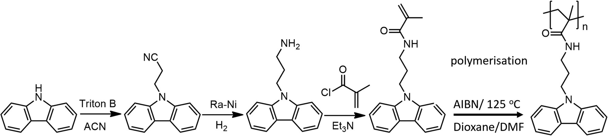 | ||
| Scheme 1 Synthesis of the N-(3-(9H-carbazol-9-yl)propyl)methacrylamide (CaPMA) and its radical polymerisation. | ||
1H NMR (300.13 MHz, CDCl3, δ): 8.07 (d, J = 7.8 Hz, 2H, carbazole), 7.49–7.43 (m, 2H, carbazole), 7.36 (d, J = 8.1 Hz, 2H, carbazole), 7.27–7.23 (m, 2H, carbazole), 4.59 (t, J = 7.20 Hz, 2H, N–CH2), 2.78 (t, J = 7.20 Hz, 2H, N–C–CH2).
FT IR: 3050, 2952, 1592, 1483, 1452, 1351, 1325, 1259, 1224, 1197, 1151, 1123, 1065, 1019, 928, 808, 744, 723, 617, 560, 541, 528 cm−1.
Yield: 55.0 g (72%). M.p. 47–48 °C (lit.1 47–48 °C). Anal. calcd for C15H16N2 (224.30): 80.32% C, 7.19% H, 12.49% N; found: 80.34% C, 7.22% H, 12.29% N. 1H NMR (300.13 MHz, CDCl3, δ): 8.09–8.06 (m, 2H, carbazole), 7.47–7.37 (m, 4H, carbazole), 7.26–7.11 (m, 2H, carbazole), 4.38 (t, J = 6.90 Hz, 2H, N–CH2), 2.71 (t, J = 6.90 Hz, 2H, N–C–C–CH2), 2.07–1.83 (m, 2H, N–C–CH2), 1.07 (br s, 2H, −NH2). 13C NMR (75.45 MHz, CDCl3, δ): 140.5, 125.7, 122.9, 120.4, 118.9, 108.7 (12C carbazole), 40.5, 39.7, 32.7 (3C aliphatic).
Yield: 6.95 g (67%). Anal. calcd for C19H2ON2O (292.37): 78.05% C, 6.89% H, 9.58% N; found: 78.0% C, 6.70% H, 9.61% N. 1H NMR (300.13 MHz, CDCl3, δ): 8.06 (d, J = 7.50 Hz, 2H, carbazole), 7.45–7.09 (m, 6H, carbazole), 5.64 (br s, 1H, NH), 5.42 (s, 1H, ![[double bond, length as m-dash]](https://www.rsc.org/images/entities/char_e001.gif) CH2), 5.17 (t, J = 1.50 Hz, 1H, CH2), 4.34 (t, J = 6.75 Hz, 2H, carbN–CH2), 3.26 (q, J = 6.60 Hz, 2H, carbN–C–C–CH2), 2.10 (pent, 2H, J = 6.75 Hz, carbN–C–CH2), 1.74 (s, 3H, CH3). 13C NMR (75.45 MHz, CDCl3, δ): 168.5 (CO), 140.2 (CCH2), 139.7, 125.9, 123.0, 120.5, 119.6, 108.6 (12C carbazole), 119.2 (CCH2), 40.9, 37.9, 28.7 (3C aliphatic), 18.5 (CH3).
CH2), 5.17 (t, J = 1.50 Hz, 1H, CH2), 4.34 (t, J = 6.75 Hz, 2H, carbN–CH2), 3.26 (q, J = 6.60 Hz, 2H, carbN–C–C–CH2), 2.10 (pent, 2H, J = 6.75 Hz, carbN–C–CH2), 1.74 (s, 3H, CH3). 13C NMR (75.45 MHz, CDCl3, δ): 168.5 (CO), 140.2 (CCH2), 139.7, 125.9, 123.0, 120.5, 119.6, 108.6 (12C carbazole), 119.2 (CCH2), 40.9, 37.9, 28.7 (3C aliphatic), 18.5 (CH3).
Yield: 1.4133 g (78%); Mw = 6000, Mn = 4000, Đ = 1.50, glass transition temperature Tg = 160 °C as determined from the DSC measurements. 1H NMR (600.27 MHz, DMSO, δ): 8.20–6.80 (m, 9H, carbazole 8H + NH), 4.06 (br s, 2H, carbN–CH2), 2.86 (br s, 2H, carbN–C–C–CH2), 1.73 (br s, 2H, carbN–C–CH2), 1.60-0.50 (m, 5H, backbone CH2 + CH3). 13C NMR (150.96 MHz, DMSO, δ): 176.8 (CO), 139.7, 125.6, 122.0, 120.2, 118.6, 109.0 (6 × 2C carbazole), 54.8, 44.6, 37.4, 27.8, 17.8, 16.2 (6C aliphatic).
Besides the polymer prepared according to the procedure described above, two other batches of PCaPMA were synthesized using different reaction times and temperatures during the radical polymerisation (see Procedures 1 and 2 in (ESI,† Section A)) but all of them had lower Mw and Mn than that one used for the study described in this paper (Procedure 3 in (ESI,† Section A)). However, no differences in the UV-vis and fluorescence spectra were observed between solutions of these batches (ESI,† Fig. S3).
Preparation of memory devices
ReRAM devices were fabricated as a sandwich structure (ESI,† Fig. S1) using an ITO on a glass substrate as a bottom electrode (BE). The ITO electrodes were patterned by chemical etching (ESI,† Section B). Before polymer deposition, the substrate was cleaned in an ultrasonic bath subsequently with deionised water, acetone, and isopropanol, each solvent for 15 minutes, dried thoroughly with compressed nitrogen gas, and treated with UV light for 20 minutes. After cleaning, the surface resistance of ITO was verified to be about 80 Ω sq−1.Polymer thin films were deposited by spin-casting using chlorobenzene solution of the respective polymer, with a concentration in the range of 10–110 mg mL−1 and with a rotation speed of 2000–4000 rpm, according to the required thickness. Before casting, the PCaPMA and PVCa solutions were filtered through PTFE membrane syringe filters subsequently with pore sizes of 220 nm and 100 nm. Depending on the solvent, solution concentration and rotation speed, films of various thicknesses were prepared, with the thickness in the range between 30 and 500 nm. Some more detailed examples of various film casting conditions are listed in Table S1, ESI.† For the solvent removal, the deposited layers were thermally cured in a vacuum (pressure 100 mbar) at 120 °C for 4 hours. Finally, a 100 nm thick Al or Au top electrode (TE) was deposited by physical vapour deposition (PVD) through a shadow mask using MiniLab 60 (Moorfield, UK) in a vacuum (10−7 mbar) with a deposition rate of 5–10 Å s−1. The active area between the electrodes was about 2 mm2. Some samples were prepared with a smaller area of 0.15 mm2 for checking the dependence of electrical characteristics on the current density.
Three different types of memory devices were fabricated. Type I and type II devices comprised of a PCaPMA active layer sandwiched between ITO and Al electrodes (ITO/PCaPMA/Al), or Au electrode (ITO/PCaPMA/Au), respectively. Type III devices had a PVCa active layer sandwiched between ITO and Al (ITO/PVCa/Al).
Characterization
Attenuated total reflectance Fourier-transform infrared (ATR FTIR) spectra of polymer thin films cast on Al foil were recorded using a Nicolet Nexus 870 FTIR spectrophotometer (ThermoScientific, Markham, Canada). The samples were measured on an ATR Golden Gate unit (Specac) equipped with a diamond prism and a controlled heated top plate in a dry-air-purged environment. The spectra were recorded at 5 °C steps in the interval 25–100 °C and at 10 °C steps between 100–150 °C, followed by cooling of the sample in 10 °C steps. NMR spectra were measured on multinuclear double-resonance NMR spectrometer 300 (Bruker DPX 300, Magritek, USA). Gel permeation chromatography was obtained on Shimadzu HPLC (Kyoto, Japan) equipped with a PDA detector.Differential scanning calorimetry (DSC) and cyclic voltammetry (CV) measurements were carried out on DSC Instruments Q2000 (Haverhill, USA) and PerkinElmer 8000 and AMEL Potentiostat (AMEL s.r.l., Milano, Italy).
X-Ray Diffraction (XRD) patterns were collected using a high-resolution Explorer diffractometer (GNR, Italy) with a Mythen 1K strip detector, operated at 40 kV and 30 mA. The measurements were performed under the CuKα radiation (wavelength = 1.54 Å) using Bragg–Brentano geometry, in a 2θ range of 2–80°, with a 0.05° step and a step time of 10 s. The peak deconvolution was carried out using the Fityk 1.3.1 program.32
Broadband dielectric spectroscopy (BDS) measurements were performed using Novocontrol Alpha A High-performance frequency analyser in combination with a QUATRO temperature controller and ZGS active sample cell (Novocontrol Technologies, Montabaur, Germany) in the frequency range 10−2–106 Hz and in the temperature range −100 °C to 170 °C for PCaPMA and −100 °C to 250 °C for PVCa, respectively, with 1 VAC applied. About 20 μm thick layers were prepared by drop-casting on a gold-plated brass disc. A second gold-coated brass disc, placed at the layer surface by heating and pressing, was used as the TE.
UV-vis absorption and photoluminescence spectra of solutions and solid-state thin films were recorded on PerkinElmer Lambda 950 spectrophotometer (Shelton, USA) and an FS5 spectrofluorometer (Edinburg Instruments, UK), respectively. The thickness and roughness of the prepared layers were observed on the KLA TENCOR P-10 surface profilometer (KLA-Tencorp, Milpitas, USA).
Keithley 2602 sourcemeter (Keithley Instruments, Solon, USA) was used for the electrical characterization of memory devices. Electrical measurements were performed either on air or inside a vacuum chamber (turbomolecular pump, Pfeiffer Vacuum GmbH, Germany) tempered using a HAAKE F6 thermostat (Thermo Haake, Karlsruhe, Germany). The devices were biased through the ITO BE, while the TE was grounded. The temperature dependences of the current–voltage characteristics were measured in the range 20–100 °C and 100–125 °C with 15 °C or 5 °C steps, respectively, allowing the sample to thermally stabilize for 15 min at each step.
3. Results and discussion
3.1. Solubility and thermodynamic properties
The PCaPMA polymer is well soluble in common organic solvents like chlorobenzene, chloroform, dioxane, and THF. Although a small weight loss of around 2% can be observed below 100 °C (originating from solvent and water residues), it follows from Fig. S2a in ESI† that the polymer is stable up to 250 °C, with the main decomposition starting at 350 °C. The DSC analysis showed a glass transition temperature Tg ∼ 151 °C (ESI,† Fig. S2b), markedly lower than the glass transition temperature Tg ∼ 220 °C of the reference PVCa. The lower value of Tg obtained for PCaPMA should be attributed to the longer spacer between the carbazole group and the polymer backbone. However, compared to poly[(3-(9H-carbazol-9-yl)propyl)methacrylate] (PPrMA, Tg = 111 °C),33 a polymer with a very similar molecular structure, having the same side chain length but missing the amide group, the Tg of our polymer is markedly higher. Analogically to the increase of Tg in polyacrylamide compared to polymethacrylate, the higher Tg of PCaPMA can be partially explained by conformational stiffness of the side group caused by the limited rotation around the C–N bond,34,35 and partially also by the physical crosslinking via hydrogen bonds formed between the amide and carbonyl groups, both on the same sidechain or intermolecularly.3.2. Infrared spectroscopy
The representative IR spectra recorded during the heating-cooling cycle are shown in Fig. 1. The HN–CO amid group in the sidechain of PCaPMA polymer is manifested through its characteristic bands. The N–H stretching band of secondary amines appears as a doublet at 3434 and 3366 cm−1. Upon heating, these peaks shifted to higher frequencies and persisted there during subsequent cooling.
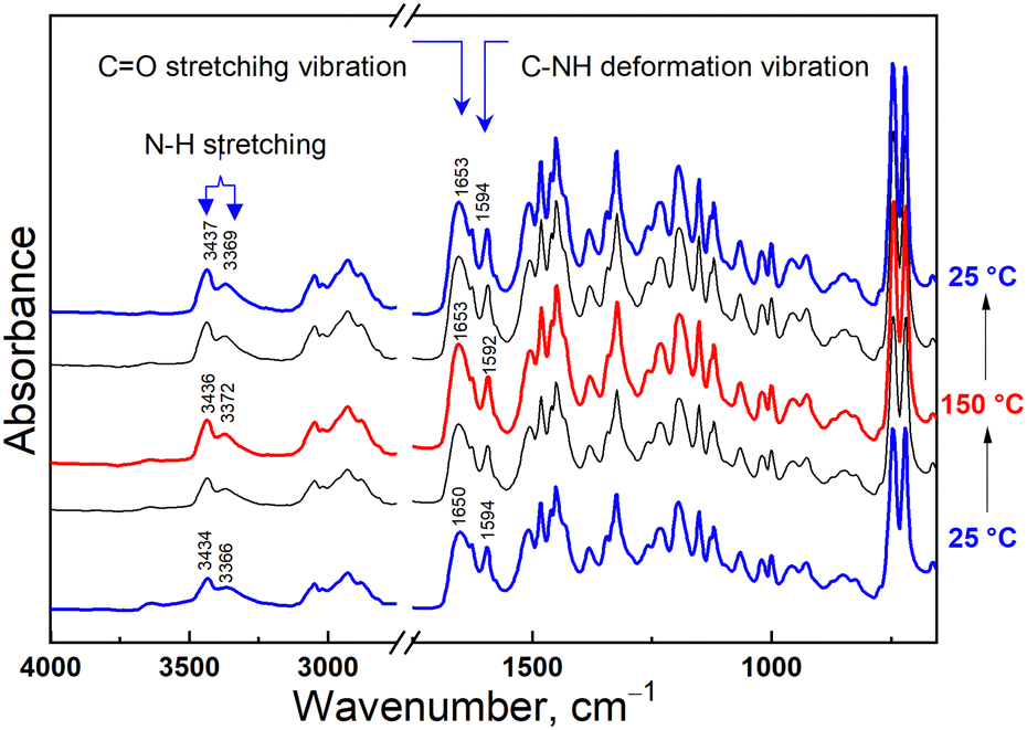 | ||
| Fig. 1 ATR FTIR spectra of PCaPMA at 25 °C, 100 °C, and 150 °C during the heating/cooling cycle. | ||
The amid I (1650 cm−1) and amide II (1594 cm−1) bands, related to the HN–CO group complex vibration, originate from the stretching and deformation vibrations of the CO and C–NH groups, respectively. The amide I peak shifts to 1653 cm−1 upon heating to 100 °C and remains at this frequency during further temperature variations. The amide II band moves to 1592 cm−1 when heated to 150 °C, and returns to 1594 cm−1 after cooling down to room temperature.
Both bands I and II are sensitive to hydrogen bonding as described, for example, in the proteins secondary structures stabilized by H-bonds, where the amid I range for β-sheet is within 1625–1640 cm−1 but for α-helix it is shifted to 1648–1660 cm−1. Similarly, in the infrared spectrum of N-methyl acetamide, there is an amide I band found at 1718 cm−1 for the glass phase, at 1653 cm−1 for the H-bonding network, and 1630 cm−1 for the aqueous solution.36 The H-bond depletes the electron density on the CO group and, consequently, decreases the amide I frequency. On the other hand, when the bending vibration of the N–H group is restricted by the hydrogen bridge, by increasing the force constant the frequency of the amide II band increases.36
The stretching vibration of the H-bonded N–H group demonstrated the most significant shift with increased temperature with the blue shift towards higher frequencies. This can be explained by the increase in the N–H bond force constant as the H-bonds disappear. This aligns with the red shift of the Amide II band at higher temperatures. Conversely, the presence of the hydrogen bridge results in a smaller force constant of the N–H bond, leading to lower frequencies of the NH band in the infrared spectrum. The carbazole out-of-plane C–H vibration related to the bands at 745 cm−1 and 720 cm−1, remains virtually unchanged throughout the heating-cooling cycle.
It is known from the literature cited above that the Amide I band frequency can vary as much as 90 cm−1 depending on the strength of the hydrogen bonds. The changes in the FTIR spectra during heating observed in PCaPMA are small, on the edge of the spectral resolution. However, the position of IR bands typical for the presence of hydrogen bonds and the shift of these bands with temperature, which was reproducible and occurred at temperatures already below 100 °C, suggest that the structure of the polymer is influenced by hydrogen bonds. The more pronounced changes reported in literature36 are due to the nature of those studied materials, and the high amount of carbonyl groups involved in their H-bonds, which are highly disturbed upon the thermal transition. The small changes observed in PCaPMA point only to their weakening at elevated temperatures due to the release in molecular motion.
3.3. X-Ray diffraction
To get an insight into the morphology of the PCaPMA polymer film its diffraction pattern was compared to the XRD of the reference PVCa. To obtain the accurate positions of the peaks, the experimental profiles were deconvoluted and fit with a Gaussian and a pseudo-Voigt function, for amorphous and crystalline phases, respectively. The XRD pattern of the PVCa powder exhibits a broad amorphous peak centred around 2θ = 19° (dashed grey line in Fig. 2) and four relatively wide peaks at 2θ = 7.71°, 9.52°, 13.09°, and 20.10°, corresponding to d-spacing of 11.5 Å, 9.3 Å, 6.8 Å, and 4.4 Å, respectively (Fig. 2). The first peak could be attributed to the interchain spacing of 11.5 Å between PVCa chains aligned together in a pseudohexagonal lattice, while the distance of 6.8 Å denotes the periodicity along the c-axis.37 The peak at 20.10° may be attributed to the X-ray diffraction on π–π stacked carbazole groups.38 In the PCaPMA spectrum, these three peaks are shifted towards lower 2θ values (wider d-spacing) equal to 6.76° (13.1 Å), 12.30° (7.2 Å), 19.86° (4.5 Å), which may have been obtained due to the presence of the PMA spacer. The first reflection is broader and less pronounced than in the case of PVCa, implying less ordered alignment between polymer chains, whereas the intensity of the 12.30° peak is much bigger than in the case of the PVCa sample, suggesting enhanced ordering of polymer chains along the c-axis. The degree of crystallinity, Xc, was estimated based on the method of Nara and Komiya,39 given by the ratio Xc = Ac/(Ac + Aa), where Ac is the area under crystalline peaks and Aa is the area under amorphous region. The degree of crystallinity was found 51.6% for PVCa and 40.6% for PCaPMA.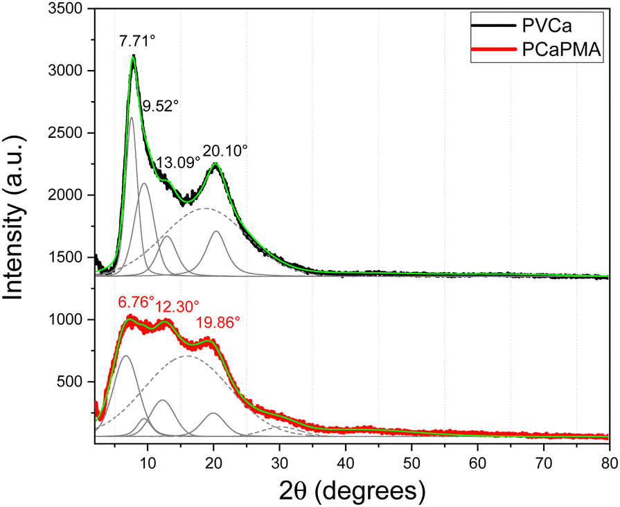 | ||
| Fig. 2 X-Ray diffractograms of PVCa (black curve) and PCaPMA (red curve) together with the peak deconvolution (green line – overall fit, solid gray line – pseudo-Voigt dashed, grey line – Gaussian peaks). The curves are vertically shifted for clarity. | ||
3.4. Optical properties
The UV-vis optical absorption and fluorescence emission spectra of PCaPMA and PVCa dissolved in DMSO and thin films cast on quartz substrates are shown in Fig. 3, all normalised to the respective maxima. Only the vibrionic peaks of the lowest electronic transition in the spectral region with wavelengths longer than 300 nm are presented. These peaks originate from the π–π* (1A–1Lb) transition of the carbazole chromophores, with the transition dipole moment aligned in the direction of the short axis of the carbazole molecule.40 Compared to PVCa, the polymer PCaPMA displayed a small shift towards lower energy, approximately 3 nm, and a very small shift of about 2 nm when going from the solution to a solid phase. Contrary to the broad and red-shifted emission band found in PVCa solution due to a stronger mutual on-chain chromophore interaction, the PCaPMA fluorescence emission spectra demonstrated an almost ideal mirror symmetry with the absorption spectra and a markedly smaller Stokes shift. The fluorescence peaks correspond to the vibrionic structure of the π–π* optical transitions of carbazole monomers, with an intense 0–0 vibronic band centred around 355 nm41,42 and a second vibronic band (0–1) around 372 nm (Fig. 3).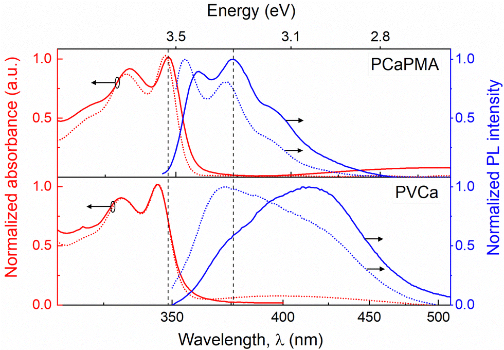 | ||
| Fig. 3 UV-vis absorption (red lines) and emission spectra (blue lines) of (a) PCaPMA and (b) PVCa in thin films (solid lines) and solutions in DMSO, concentration 10−5 M (dashed lines). | ||
In the solid state, there is an increased Stokes shift and the 0–1 band becomes more intense, indicating considerable structural changes in the excited state compared to the ground state. Conversely, PVCa in DMSO solution exhibited a more intense monomeric emission peak around 373 nm and a small broad shoulder around 414 nm pointing to a weak mutual interaction between chromophores in solution. This band increased significantly in a solid state, suggesting the sandwich-type of mutual interactions between carbazole groups, resulting from the overlap of adjacent π-orbitals from intra-chain excimer formation.23,40,41,43,44 Notably, PCaPMA spectra lack this excimer emission, in good agreement with its less ordered structure compared to PVCa, as observed in XRD diffractograms (Fig. 2).
It is known from the literature that, in addition to the mutual interaction of neighbouring molecules in solid state, the positions of the optical bands of carbazole groups depend on their chemical substitution. However, in our case the differences in the optical spectra between PCaPMA and PVCa observed in thin layers are relatively large compared to solution, and therefore we attributed this effect to a different packing of the carbazole molecules in the layer, rather than to the electronic effect observed by other authors on carbazoles substituted with alkyl groups.27 In PCaPMA, besides a higher flexibility of the side groups, the bulky side chains decrease the concentration of chromophores, which also contributes to a lower probability of the excimer formation.42
The absorption and emission spectra were found to be insensitive to the polymerisation conditions within the range of reaction conditions used in our study. All three molecular weights of PCaPMA exhibit identical spectra (ESI,† Fig. S3). For further investigation, we exclusively used the polymer with the highest molecular weight, which also provided the best pinhole-free thin films by spin-casting deposition (ESI,† Fig. S4).
3.5. Cyclic voltammetry (CV)
The cyclic voltammograms of the 30–45 nm thick PCaPMA and PVCa polymer layers cast on an ITO/glass substrate electrode and immersed in a 0.1 M acetonitrile solution of n-Bu4NPF6, measured at a scanning rate of 20 mV s−1, are presented in Fig. 4a. A Pt wire was used as a counter electrode, and Ag/AgCl as a reference electrode. For PCaPMA, the anodic scan reveals an oxidation peak at approximately 1.37 V with an onset of about 0.81 V, while in PVCa, the onset appears at approximately 0.92 V. The highest-occupied molecular-orbital energy level (HOMO) was calculated using eqn (1):29| EHOMO = −[(EOX(onset) – EOX(onset),FER) + 4.8] eV | (1) |
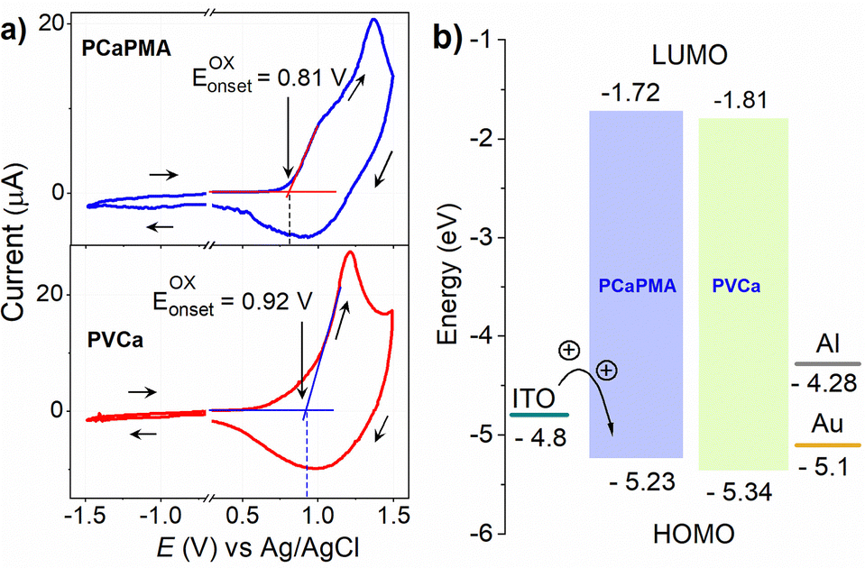 | ||
| Fig. 4 (a) Cyclic voltammogram (CV) of PCaPMA (top) and PVCa (bottom) cast on the ITO electrode. The scan rate was 20 mV s−1, sweep direction indicated by arrows, (b) energy levels diagram of polymers and electrodes. | ||
From these measurements, the energy position of the HOMO level of PCaPMA was determined as EHOMO = −5.23 eV, slightly higher than PVCa, where the value EHOMO = −5.34 eV was obtained, consistent with previous literature reports.29,45,46
Both polymers displayed CV curves that were not fully reversible and exhibited only weak reduction peaks. The bandgap, Eg, was therefore determined from the Tauc plot of the optical absorption spectra. The bandgap for PCaPMA was found to be 3.51 eV, which is only 0.02 eV, i.e. less than the kT value, smaller than that of PVCa. Using the above values, the energy of the lowest-unoccupied molecular-orbital (LUMO) levels were calculated as −1.72 eV and −1.81 eV for PCaPMA and PVCa, respectively. The energy diagram is shown in Fig. 4b.
3.6. Broadband impedance spectroscopy
The impedance spectra of PCaPMA polymer clearly show three distinct relaxation processes labelled as α, β and γ relaxations. These relaxations were distinctly visible in frequency/temperature-dependent loss modulus shown in Fig. 5a. These patterns are similar to those observed in poly[11-(9H-carbazol-9-yl)alkyl methacrylate]s by Bandera Y. et al.47 and McFarlane T. M. et al.33 but they differ in higher-temperature relaxations, namely α-relaxation related to the glass transition temperature, Tg, and its merging with β-transition (αβ-merging). In PCaPMA. We observed a weak band of γ-relaxation (between −90 °C and 0 °C), a strong β-relaxation band (between 0 °C and 140 °C), and an α-relaxation band (between 60 °C and 170 °C). In previous studies on methacrylate-based polymers, such as reported by J. Kolařík et al.48 and J. M. Pochan et al.,49 the γ-relaxation was attributed to the motion of end groups (rotational freedom of the pendant carbazole group), the β-transitions to the relaxation of side chain conformation around the C–C bond connecting the main and the side chains as well as the wagging motions of the carbazole unit, and the α-relaxation to the segmental motion of the main chain. Similar to this series of polymers, PCaPMA also exhibited an increase in intensity and temperature of the γ-relaxation compared to PVCa due to the increased volume fraction of the sidechains. The relaxations were found to be thermally activated processes33 and their activation energies, Ea, were determined from the Arrhenius plots of the frequency of the maxima of the respective relaxation, fmax, versus reciprocal temperature as shown in Fig. 5b. Table 1 summarizes the activation energies of all three discussed relaxations together with the glass transition temperatures obtained from the DSC measurements for both polymers.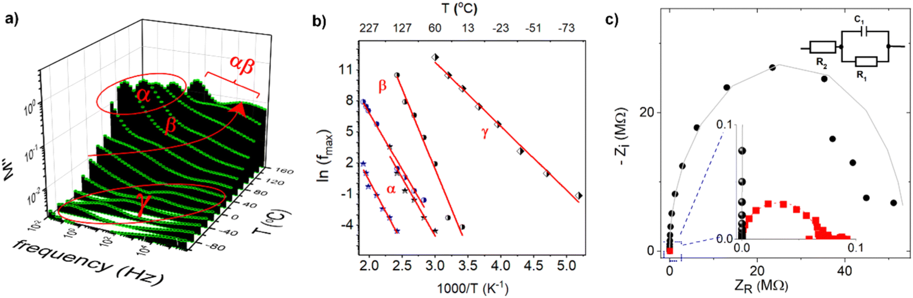 | ||
| Fig. 5 (a) Temperature dependences of the spectra of the loss modulus M′′ of PCaPMA, (b) Arrhenius plot of the frequency of the maxima of the loss modulus spectra for α-, β- and γ-relaxations of PCaPMA (black symbols) and PVCa (blue symbols), respectively, (c) Nyquist plot of the complex impedance of the pristine sample (black circles), and of the sample after application of the DC voltage +5 V (red squares) in the zoomed view of high frequency region. Experimental points were fitted using equivalent circuit shown in the inset with fitting parameters: R2 = 5.4 × 10⁷ Ω (pristine), R2 = 6.5 × 10⁵ Ω (after application of DC voltage); C = 1.2 × 10 −9 F and R1 = 80 Ω in both cases. | ||
| Material | Glass transition temperature, Tg | Activation energy, Ea | |||||
|---|---|---|---|---|---|---|---|
| α- relaxation | β- relaxation | γ-relaxation | |||||
| (°C) | (kJ mol−1) | (eV) | (kJ mol−1) | (eV) | (kJ mol−1) | (eV) | |
| PVCa | 220 | 99.4 | 1.03 | 90.7 | 0.94 | — | |
| PCaPMA | 151 | 93.1 | 0.96 | 128.4 | 1.33 | 51.2 | 0.53 |
As the temperature increased, all relaxation maxima shifted towards higher frequencies. The γ-relaxation in PCaPMA occurred at a higher temperature compared to PPrMA (polymer with the same length of the side chain but missing the amide group), where the γ relaxation was observed in the temperature interval between −150 °C and −70 °C, with Eγ = 45.3 kJ mol−1. This difference can be attributed to the formation of hydrogen bonds in the side chain48 and it is in accord with the similar finding in IR spectroscopy. However, a decrease in the activation energy of the β-transition (Eβ = 128.4 kJ mol−1) for PCaPMA compared to PPrMA (Eβ = 152.6 kJ mol−1) is not fully understood. At higher temperatures, above 120 °C, the α-transition merges with β-relaxation as observed by R. Bergman et al. in polymethylmethacrylates with longer side chains.50
Besides the temperature dependences of the loss modulus (M′′) that best illustrate the relaxation modes of the polymer, we also measured the temperature dependence of the spectra of the dielectric constant, ε′ (see ESI,† Fig. S5). The value ε′ = 3.1 (1 kHz) was found from these measurements at room temperature.
To elucidate the phenomena responsible for resistance switching invoked by the applied voltage, we measured the real and imaginary part of the impedance on a fresh sample (ITO/PCaPMA 80 nm/Al) and the same sample after applying the DC voltage sweep from 0 V to +5 V. The impedance data were analysed using the Nyquist plot (Fig. 5c) and an equivalent electronic circuit model consisting of parallel R2C combination in a serial connection with a resistor R1 (see inset of Fig. 5c). As can be seen from the fitted parameters, only the real part of the impedance has been changed after switching between two conducting states of the device. For both conducting states, an identical value for the capacitance C was obtained as well as for the serial resistance R1. It shows that the interface electrode effects or changes in the injection barrier, possibly formed by Al2O3,51,52 do not play a role in the switching mechanism. Similarly, the unchanged value of capacitance in the pristine and in the voltage-loaded sample suggests that no dielectric breakdown occurred in the active layer.53
3.7. Electrical characterization
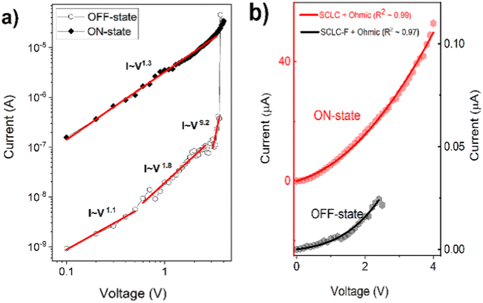
The DC current–voltage (I–V) characteristics of the sandwich devices containing active layer made of PCaPMA (devices I and II) and PVCa (device III) are depicted in Fig. 6. All measurements were performed under ambient conditions at room temperature in the dark unless otherwise stated. The typical electrical measurements were performed by sweeping the voltage in the course 0 V → +Umax → −Umax → 0 V. Two subsequent cycles are shown in each figure. The sign/polarity of the voltage refers to the bottom ITO electrode. The presented I–V characteristics were obtained from devices with an 80 nm thick active layer but similar results were observed for devices with active layer thicknesses ranging between 80 and 190 nm.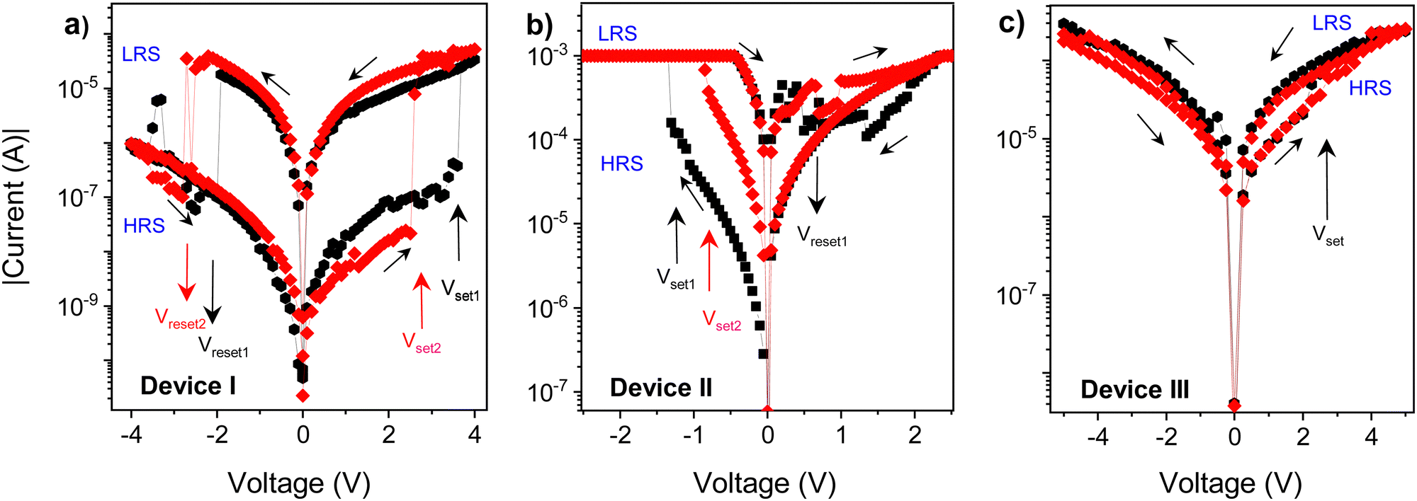 | ||
| Fig. 6 Two subsequent cycles of current–voltage (I–V) characteristics of (a) device I (ITO/PCaPMA/Al), (b) device II (ITO/PCaPMA/Au), and (c) device III (ITO/PVCa/Al) black – 1st cycle, red – 2nd cycle. The thickness of the active layer was ∼80 nm, and voltage sweep rate of 0.05 V s−1 in all cases, sweep direction indicated by the respective arrows. The sign of the applied voltage refers to the bottom ITO electrode. The current compliance value IC = 10−2 A was set for devices I and III, and IC = 5 × 10⁻³ A for device II. HRS and LRS stands for high- and low-resistance state, respectively. Vset and Vreset stands for the threshold voltage in which the resistance changes to LRS and HRS, respectively. | ||
As shown in Fig. 6a, the device I exhibited a repeatable bistable switching behaviour between a high resistance (HR) state and a low resistance (LR) state, with the difference in the resistance exceeding two orders of magnitude. During the positive voltage sweep, when the applied voltage reached a threshold value, VT, the current increased from the HR to the LR state, which could be switched back to the HR state by reversing the voltage polarity. In the first positive bias sweep, 0 → +4 V, the current abruptly increased from HR (OFF state) current ∼10−8 A to ∼10−5 A at about +3.6 V. The LR (ON state) state current was at least 100 times higher than at the OFF state, and in some samples, the ON/OFF current ratio exceeded 104. Such current ON/OFF ratios, 102–104, exceptionally even 105, have been reported for rewritable memories made of similar polymer materials but they mostly compromise their rewritable ability or nonvolatility.7,17,18 During the reverse sweep (4 → 0 V), the device remained ON. However, in the subsequent sweep to the negative applied voltage (0 → − 4 V), the device resets back to the HRS with a resetting voltage of about −2.3 V.
In subsequent I–V cycles, the setting voltage decreased slightly, which could be attributed to easier conformational changes in the sidechains after the 1st cycle, similar as described by the Ling group.10 The setting and resetting processes were not abrupt but continuous in some cells, leading to a negative differential resistance (NDR), which was dominant at fast scan rates, above 10 V s−1. VT ranged from 2 to 4.5 V among devices but most devices with ∼80 nm thick layers switched around 2.7 V. Additionally, some variations in other electrical parameters, such as the current in the HRS and LRS, ON/OFF current ratio, resetting voltage, and device performance were observed from sample to sample. Around 30% of the samples failed to show reproducible characteristics; as they were either short-circuited or showed only a WORM behaviour. The limited reliability might be due to the electrical breakdown of the active layer caused by the substrate inhomogeneity or the formation of pinholes due to the very small thickness of the active layer.
Devices with Au top electrode (device II) also exhibited a hysteresis in the current–voltage characteristics, but the threshold voltage VT was noticeably lower, and the current was higher in both the LR and HR states compared to the device I (Fig. 6b). Setting the compliance limit ICL was necessary to prevent electrical breakdown, and setting it to values higher than 5 × 10⁻³ A mostly resulted in permanent electrical breakdown of the sample. The lower VT and higher current could be attributed to a lower Schottky barrier between the HOMO level of PCaPMA and the work function of gold, compared to ITO (see Fig. 4b). Moreover, a relatively high current was observed even in the OFF state and the electrical breakdown above ICL indicates the possibility of the gold diffusion into the bulk of the sample during the vacuum deposition of Au, forming filaments or nanoparticles that penetrate the polymer layer. As suggested by J. G. Simmons and R. R. Verderber,54 this diffusion can change the electrical characteristics of the device, mainly decreasing the bulk resistance.
In contrast to the devices made of PCaPMA, the device III, having the PVCa active layer, switched from HR to LR state after the threshold voltage had been reached, and it remained permanently in the ON state during further cycling. Even when higher voltages were applied with both polarities, no recovery of the OFF state was observed. Hence, device III behaves as a write-once-read-many times (WORM) memory, which has been previously reported in the literature for pure PVCa17,30 or PVCa composites.55
3.8. Memory device performance
The dynamic switching characteristics of the device I, involving the “write-read-erase-reread” (WRER) process are illustrated in Fig. 7a. The device underwent more than 200 cycles in this test, with +5 V used to switch the device from the HR to the LR state, and −5 V for resetting it back to the HR state. Both voltages were chosen slightly higher than the minimum switching and resetting voltages to ensure the complete transition of the device resistance. After each setting and resetting, the current was measured at the applied voltage of +0.5 V for 60 seconds. The extended reading time in both states was employed to check the persistence of the current level. The device remained electrically stable over 200 WRER cycles. However, after 40 measurement cycles, some partial failure in switching/erasing was observed along with the gradual decrease in conductance of about 10%.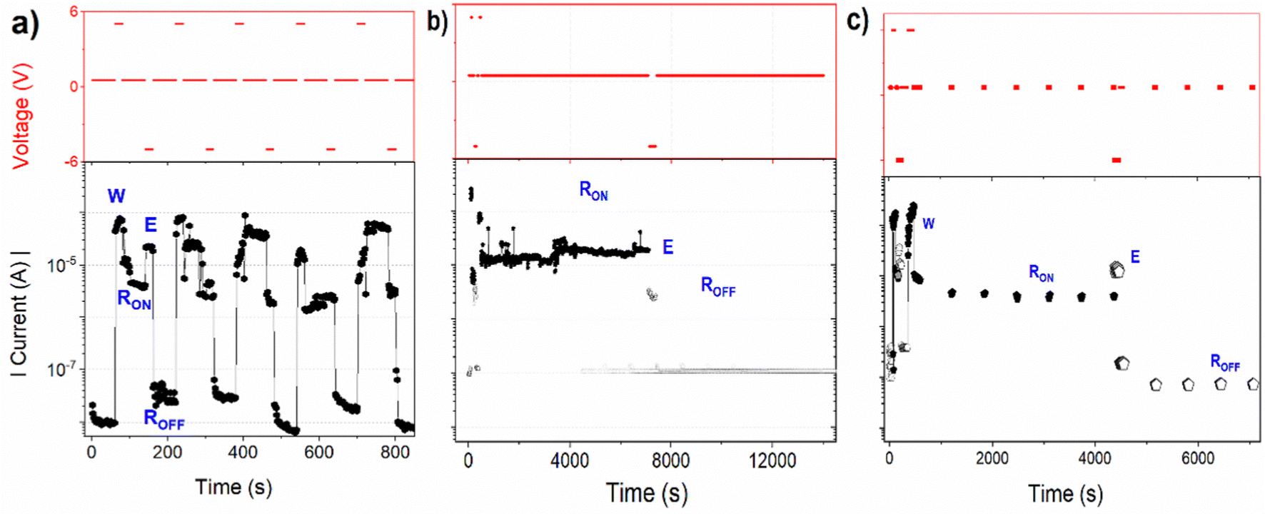 | ||
| Fig. 7 The memory behaviour of the device I, (a) dynamic test with repeated write-read-erase-reread (WRER) cycles, (b) persistence test of both ON and OFF states under constant voltage stress +0.5 V, (c) volatility test. The time course of voltage pulses is shown in red in the upper charts, and the corresponding current response in black colour in the bottom graphs. W, E, RON, and ROFF indicate writing (setting), erasing (resetting), and reading in the LR (ON) state and reading in the LR (OFF) state, respectively. (a) and (b) show the measurements in ambient conditions while (c) was measured in vacuum (pressure 5 × 10⁻⁴ mbar). | ||
To assess the stability or persistence of the device, current measurements in both states were conducted also at the permanently applied +0.5 V (Fig. 7b). The current was found to remain stable for up to 2 h, maintaining the current ON/OFF ratio higher than 100. Both the dynamic WRER and the persistence tests were carried out in the dark and under ambient conditions.
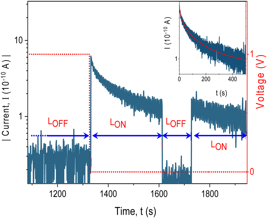
In addition to the persistence, a volatility test was conducted, too. In this test, device I was initially set to the ON state at + 5 V, and then the current was measured at +0.5 V every 10 minutes, with the applied voltage turned off between measurements (Fig. 7c). The test was first performed under vacuum conditions (pressure < 10−4 mbar). After setting the device to the LR state, the current initially decreased, being reduced to about one-half of the current measured immediately after setting the device to the ON state. However, over a longer duration only a small decrease, less than 5%, was observed, indicating a promising retention ability of the device.
The device was also tested under ambient conditions. During this test, several cycles with the voltage sweep 0 → +4 V were recorded with an increasing period between cycles (ESI,† Fig. S6). After the first sweep that switched the device to the ON state at about +3.5 V, the sample was left to relax without the applied voltage for the increasing period between subsequent cycles. During the following sweep after a minute, the I–V characteristics followed the ON state current with only a negligible decrease. However, after 10 minutes of relaxation, the subsequent sweep showed a decrease in current almost an order of magnitude, but the ON state was recovered at about +1.2 V. This markedly smaller value of the voltage setting the device back to the ON state can be understood since the device was not fully reset to the HR state (OFF state) between these cycles. As the time delay between the sweeps increased, the current at a smaller applied voltage decreased, reaching only one hundredth of the ON value after 14 hours of relaxation. The retention capability of the memory device is thus markedly worse in ambient conditions compared to vacuum. However, the ON/OFF ratio of around 50 observed after 14 hours is still quite convincing, indicating that the device retains its memory state to a significant period of time even under ambient conditions.
4. Resistive switching mechanism
For explaining the mechanism of resistive switching several phenomena have to be considered, which were addressed by additional experiments.4.1. Resolving the resistance switching mechanism
First, we wanted to exclude the effect of the electrode oxide layer naturally formed in the air at the Al electrode/polymer interface. For this, the electrical characterization of the memory device was performed inside the evaporation vacuum chamber (pressure ∼10−7 mbar) immediately after depositing the Al top electrode. Before the electrode deposition, the sample was placed in the evacuated vacuum chamber for 48 h to release any trapped oxygen and moisture from the layer. This device showed similar resistance switching behaviour as the device stored and measured in the ambient conditions, with about one order of magnitude higher current in both ON and OFF states. This suggests that a mechanism based on the conducting filament (CF) formation supported by the presence of oxides at the electrode/polymer interface as suggested by H. L. Gomes et al.,56 is not likely. The identical characteristics observed inside the vacuum support the idea that the resistance switching can be attributed to changes in the polymer material properties rather than to the metal oxide.We further compared the I–V characteristics for two samples with different electrode active areas, namely 2 mm2 and 0.15 mm2. The same ON state current density was obtained in both cases (ESI,† Fig. S7), indicating the absence of any localized conducting filament and electrical breakdown that could be responsible for the higher current in the LR state.
4.2. Analysis of the charge transport mechanism
Due to the small Schottky barrier between the work function of ITO and HOMO of the PCaPMA polymer, compared to the barrier height between LUMO and opposite Al electrode (Fig. 4b), the injection of holes is favourable at positive applied voltage. The saturated backbone of the polymer suggests that the polymer is nearly insulating, with only negligible free charge carrier concentration in thermal equilibrium, making the electrical current space charge limited (SCLC).57,58 This SCLC is usually affected by localized states inside the bulk of the layer and, hence, it is trap-controlled.59To confirm the space charge limited nature of the charge transport, we plotted the first sweep of the I–V cycle measured on the device I in a double-logarithmic scale. The data presented in Fig. 8a show several different linear regions that can be fitted with different slopes, pointing to different current regimes. In the OFF state, between 0 and 0.6 V, a typical Ohmic conduction I ∝ Vm with m = 1 dominates.16,57 In the voltage range 0.7–3 V, below the setting voltage, the slope increased to m ∼ 2 suggesting the trap-controlled SCL current.59 At the setting voltage VT, the electric field shifts the quasi-Fermi level above the energy of traps and, consequently, to the trap-free SCLC conduction responsible for the LR (ON) state. The device remains in the trap-free SCLC regime as the voltage decreases but with an increasing contribution of Ohmic conduction below the VT value. It stays in this LR state until the voltage drops below the negative reset value.
 | ||
| Fig. 8 (a) Linear fitting of the first I–V cycle of the device I in log–log scale, (b) fitting of measured I–V curves (dots) of the device I in the OFF and ON state using eqn (2) and (3) (lines). | ||
The device kept its LR state even when the power was turned off, behaving as a nonvolatile memory device. The reverse bias was used to bring the device to its original OFF state by eliminating the previously formed space charge and emptying the filled trapping sites by neutralizing them with electrons.18
The above analysis was even better illustrated by the more accurate fitting of the I–V characteristics plotted in linear scales using analytical formulas for respective regions (Fig. 8b). The experimental data were fitted using several possible charge transport mechanisms, such as SCLC, or SCLC with field dependent mobility (SCLC-F), combined with Ohmic or Schottky contact behaviour. Since the field-dependent mobility was reported in the literature for similar carbazole-based polymers,60 obtained directly from the time-of-flight measurements, we adopted the SCLC-F model, typical for dispersive hopping transport,61 and the Ohmic dependence:28
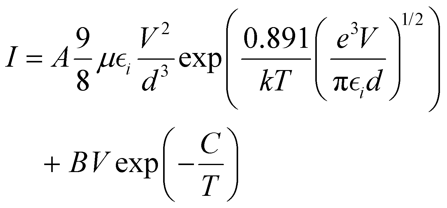 | (2) |
 | (3) |
Additional information about the charge carrier transport mechanism was obtained from the temperature dependence of the ON and OFF state currents. The temperature dependence was recorded on the device I, with the 80 nm thick polymer layer (ESI,† Fig. S8). First, we measured the OFF state at 1 V and then in the ON state at 5 V. The conductivity of the PCaPMA polymer in the ON state was almost temperature independent, similar to the observation made by Kondo et al.63 on the PVCa layer cast on a silver-modified ITO substrate. It shows that the localized states are mostly occupied and the hopping transport is less influenced by the energy barrier between hopping states. It is also in agreement with the above current–voltage characteristics with electric field independent mobility. In contrast, the device showed semiconducting behaviour in the OFF state, with the current increasing with temperature. The activation energy calculated from the Arrhenius plot of the temperature dependence of the current was determined to be Ea = 0.33 eV.
These measurements suggest that the resistive switching mechanism originates from the trapping/detrapping process. However, the observed non-volatility of the device cannot be explained solely by thermally activated detrapping from the trap with a depth of 0.33 eV. There must be some other mechanism stabilizing the LR state. This supporting mechanism is likely related to the reorientation of carbazole groups in the side chains induced by the applied voltage facilitating the charge transfer between adjacent chromophores.23,64,65 The LR state is then stabilized by the hydrogen bonds. The near Ohmic response with a slight SCLC contribution at higher applied voltage is consistent with this mechanism.
The small decrease in current over time observed in both the vacuum and ambient conditions could be attributed to the thermally activated release of carriers from shallow traps localized in the bulk or close to the polymer/electrode interface or changes in the carbazole conformation.10,17
4.3. Trapped charge evaluation by photo-detrapping
To further investigate and validate the presence of trapping centres and to determine the concentration of trapped charge carriers, we conducted an electric field-induced trapping and optical detrapping experiment on Device I, inspired by the work performed by Q. Chen et al.66 In this experimental setup, the traps were initially filled with charge carriers by applying voltage +1 V to the ITO electrode for a specific duration. Subsequently, the sample was connected to the electrometer, and the current was recorded under short-circuit conditions while being illuminated with light from a Xenon lamp equipped with a thermal and bandpass filter transmitting light in a 300–400 nm region. The discharge current under illumination was measured as a function of time (Fig. 9). The current decayed in time asymptotically following the stretched exponential dependence I = I0![[thin space (1/6-em)]](https://www.rsc.org/images/entities/char_2009.gif) exp(−(tα)/τ) with α = 0.5, τ = 6.8 s (inset of Fig. 9) until the traps are emptied. No current observed under the same illumination conditions without prior application of voltage (ESI,† Fig. S9) proves the origin of the current being in trapped charges. Since the current was seen only in the wavelength range where the carbazole chromophore absorbs light, it can be explained by the removal of the space charge trapped in localized energy levels within the bandgap by free charges photogenerated intrinsically in the polymer. By integrating the discharge current, we determined the amount of stored charge in the 80 nm thick film to be approximately 1018 charges per cm3.
exp(−(tα)/τ) with α = 0.5, τ = 6.8 s (inset of Fig. 9) until the traps are emptied. No current observed under the same illumination conditions without prior application of voltage (ESI,† Fig. S9) proves the origin of the current being in trapped charges. Since the current was seen only in the wavelength range where the carbazole chromophore absorbs light, it can be explained by the removal of the space charge trapped in localized energy levels within the bandgap by free charges photogenerated intrinsically in the polymer. By integrating the discharge current, we determined the amount of stored charge in the 80 nm thick film to be approximately 1018 charges per cm3.
 | ||
| Fig. 9 Charging by applied DC voltage and photodetrapping of trapped space charge by illumination of device I (blue line). Applied voltage showed as the red dotted line. Inset: The time course of the discharge current in a semilogarithmic plot fitted with the stretched exponential function (red line). Sample thickness 80 nm, electrode area 2 mm2, illumination through the glass/ITO side using Xe-lamp equipped with a bandpass filter, light intensity 400 μW cm−2. LOFF – in the dark, LON – under illumination. | ||
It can be seen also from Fig. 9 that the discharge current did not change after the illumination had been interrupted for about two minutes but it continued at the same value. It shows that charges are trapped in deep levels with a low escape rate. The charging/light-induced discharging cycle has been found fully reversible. This experiment strongly supports the trapping/detrapping process as the underlying mechanism responsible for the resistive switching behaviour of the device with the long persistence of the resistive state.
5. Conclusion
A new polymer, poly[N-(3-(9H-carbazol-9-yl)propyl)-methacrylamide] (PCaPMA) was prepared by radical polymerization. By the optimization of the initiator concentration, temperature and polymerization time, a sufficient molar mass of the polymer was achieved for casting compact pinhole-free layers suitable for electrical measurements. Contrary to PVCa, the polymer shows molecular dynamics determined by an interplay of the free movement of the sidechains, limited rotation around the C–N bond, and their stabilization by intra- and intermolecular hydrogen bonds. It explains its Tg value, which is lower compared to the reference PVCa but higher than a similar polymer with the equally long side group but missing the amide group. Compared to PVCa, the PCaPMA polymer shows less crystallinity and less ordered alignment between polymer chains, but enhanced ordering of polymer chains along the c-axis. It results in a weaker intermolecular interaction between carbazole groups which is also in agreement with the missing excimer emission. The sandwiched structures incorporating the PCaPMA as an active layer between ITO and Al or Au electrodes exhibited hysteresis in their volt-amp characteristics. The resistance could be switched by an applied voltage between two distinct bistable states, making the polymer applicable in ReRAM resistive memory devices. Such ReRAM showed resistive switching with a significant current ON/OFF ratio of more than 100, and satisfactory retention time in hours under ambient conditions even without the device encapsulation.Based on the experimental findings, it has been concluded that the resistive switching is caused by the bulk properties of the polymer and does not originate in electrode interface phenomena. The combination of several experiments, and particularly the photodischarge experiment performed in the low resistance state, points to trapping/detrapping of charges as the main switching mechanism with the involvement of the physical crosslinking via hydrogen bonds, which are likely to be responsible for the long persistence time of the memory state. The comprehensive understanding of these mechanisms opens up possibilities for the development of nonvolatile memory devices with enhanced performance and stability.
Author contributions
YRP: investigation – device design and preparation, electrical, dielectric and optical study, writing original draft, JP: conceptualization, funding acquisition, supervision and writing – review & editing, DV: investigation - polymer design and synthesis, AP: investigation – electrochemical measurements, MAT: investigation – optical spectroscopy, IŠ: investigation – IR spectroscopy, MK: investigation – structural XRD analysis, SHF: validation.Conflicts of interest
There are no conflicts to declare.Acknowledgements
The authors thank the MEYS (project LTAUSA19066), GAUK (project number: 474122), and the institutional support of the Czech Academy of Sciences, RVO 61389013, for funding the work. The authors also thank David Rais, PhD for his help in the conceptualization of this work, Martina Nevoralová, PhD for the TGA and Michaela Vyroubalová, PhD for the DSC measurements.Notes and references
- Z. Shen, C. C. Zhao, Y. Qi, W. Xu, Y. Liu, I. Z. Mitrovic, L. Yang and C. C. Zhao, Nanomaterials, 2020, 10, 1–31 Search PubMed.
- F. Zahoor, T. Z. Azni Zulkifli and F. A. Khanday, Nanoscale Res. Lett., 2020, 15, 90 CrossRef CAS PubMed.
- H. Andersson, A. Manuilskiy, J. Sidén, J. Gao, M. Hummelgård, G. V. Kunninmel and H. E. Nilsson, Mater. Res. Express, 2014, 1, 035021 CrossRef CAS.
- D. H. Lien, Z. K. Kao, T. H. Huang, Y. C. Liao, S. C. Lee and J. H. He, ACS Nano, 2014, 8, 7613–7619 CrossRef CAS PubMed.
- S. Lee, S. Kim and H. Yoo, Polymers, 2021, 13, 3774 CrossRef CAS PubMed.
- Y. Chen, G. Liu, C. Wang, W. Zhang, R. W. Li and L. Wang, Mater. Horiz., 2014, 1, 489–506 RSC.
- D. He, H. Zhuang, H. Liu, H. Liu, H. Li and J. Lu, J. Mater. Chem. C, 2013, 1, 7883–7889 RSC.
- E. Ryndin, N. Andreeva and V. Luchinin, Micromachines, 2022, 13, 98 CrossRef PubMed.
- W. Banerjee, X. Zhang, Q. Luo, H. Lv, Q. Liu, S. Long and M. Liu, Adv. Electron. Mater., 2018, 4, 1–7 Search PubMed.
- Q. D. Ling, D. J. Liaw, E. Y. H. Teo, C. Zhu, D. S. H. Chan, E. T. Kang and K. G. Neoh, Polymer, 2007, 48, 5182–5201 CrossRef CAS.
- F. Cai, J. M. Correll, S. H. Lee, Y. Lim, V. Bothra, Z. Zhang, M. P. Flynn and W. D. Lu, Nat. Electron., 2019, 2, 290–299 CrossRef CAS.
- Q. Xia and J. J. Yang, Nat. Mater., 2019, 18, 309–323 CrossRef CAS PubMed.
- G. Indiveri, B. Linares-Barranco, R. Legenstein, G. Deligeorgis and T. Prodromakis, Nanotechnology, 2013, 24, 384010 CrossRef PubMed.
- Y. P. Lin, C. H. Bennett, T. Cabaret, D. Vodenicarevic, D. Chabi, D. Querlioz, B. Jousselme, V. Derycke and J. O. Klein, Sci. Rep., 2016, 6, 1–12 CrossRef PubMed.
- T. McFarlane, Y. Bandera, B. Grant, B. Zdyrko, S. H. Foulger, J. Vilčáková, P. Sáha and J. Pfleger, Adv. Electron. Mater., 2020, 6, 1–10 Search PubMed.
- Y. Sun, L. Li, D. Wen and X. Bai, Org. Electron., 2015, 25, 283–288 CrossRef CAS.
- S. L. Lim, Q. Ling, E. Y. H. Teo, C. X. Zhu, D. S. H. Chan, E. T. Kang and K. G. Neoh, Chem. Mater., 2007, 19, 5148–5157 CrossRef CAS.
- S. Yanmei, A. Chunpeng, L. Junguo, L. Lei, W. Dianzhong and B. Xuduo, Thin Solid Films, 2016, 598, 293–298 CrossRef.
- Y. Liu, N. Li, X. Xia, Q. Xu, J. Ge and J. Lu, Mater. Chem. Phys., 2010, 123, 685–689 CrossRef CAS.
- Y. Yang, H. Lu, J. Liu and Y. Shen, Eur. Polym. J., 2018, 108, 10–19 CrossRef CAS.
- C. A. Walsh and D. M. Burland, Chem. Phys. Lett., 1992, 195, 309–315 CrossRef CAS.
- F. Pan, S. Gao, C. Chen, C. Song and F. Zeng, Mater. Sci. Eng., R, 2014, 83, 1–59 CrossRef.
- J. Vandendriessche, S. Toppet, N. Boens, F. C. De Schryver, P. Palmans and H. Masuhara, J. Am. Chem. Soc., 1984, 106, 8057–8064 CrossRef CAS.
- N. Tsutsumi, Polym. J., 2016, 48, 571–588 CrossRef CAS.
- P. Lova, H. Megahd, P. Stagnaro, M. Alloisio, M. Patrini and D. Comoretto, Appl. Sci., 2020, 10, 4122 CrossRef CAS.
- M. Nisoli, V. Pruneri, V. Magni, S. De Silvestri, G. Dellepiane, D. Comoretto, C. Cuniberti and J. Le Moigne, Appl. Phys. Lett., 1994, 65, 590–592 CrossRef CAS.
- C. Colombi, D. Comoretto, C. Cuniberti, G. Musso, P. Piaggio, G. Dellepiane, M. Novi, C. Dell’Erba and A. Bolognesi, Macromol. Chem. Phys., 1996, 197, 1241–1253 CrossRef CAS.
- L. H. Xie, Q. D. Ling, X. Y. Hou and W. Huang, J. Am. Chem. Soc., 2008, 130, 2120–2121 CrossRef CAS PubMed.
- Z. Li, M. Wang, H. Li, J. He, N. Li, Q. Xu and J. Lu, J. Mater. Chem. C, 2017, 5, 8593–8598 RSC.
- J. Lin and D. Ma, Appl. Phys. Lett., 2008, 93, 10–13 Search PubMed.
- F. C. Whitmore, H. S. Mosher, R. R. Adams, R. B. Taylor, E. C. Chapin, C. Weisel and W. Yanko, J. Am. Chem. Soc., 1944, 66, 725–731 CrossRef CAS.
- M. Wojdyr, J. Appl. Crystallogr., 2010, 43, 1126–1128 CrossRef CAS.
- T. M. McFarlane, B. Zdyrko, Y. Bandera, D. Worley, O. Klep, M. Jurča, C. Tonkin, S. H. Foulger, J. Vilčáková, P. Sáha and J. Pfleger, J. Mater. Chem. C, 2018, 6, 2533–2545 RSC.
- A. Karali, P. Dais, E. Mikros and F. Heatley, Macromolecules, 2001, 34, 5547–5554 CrossRef CAS.
- C. R. Kemnitz and M. J. Loewen, J. Am. Chem. Soc., 2007, 129, 2521–2528 CrossRef CAS PubMed.
- Y. Maeda, T. Higuchi and I. Ikeda, Langmuir, 2000, 16, 7503–7509 CrossRef CAS.
- C. H. Griffiths, J. Polym. Sci., Polym. Phys. Ed., 1975, 13, 1167–1176 CrossRef CAS.
- H. Li, Z. Wang, C. Song, Y. Wang, Z. Lin, J. Xiao, R. Chen, C. Zheng and W. Huang, J. Mater. Chem. C, 2014, 2, 6946–6953 RSC.
- S. Nara and T. Komiya, Starch - Stärke, 1983, 35, 407–410 CrossRef CAS.
- P. de Sainte Claire, J. Phys. Chem. B, 2006, 110, 7334–7343 CrossRef PubMed.
- G. E. Johnson, J. Chem. Phys., 1975, 62, 4697–4709 CrossRef CAS.
- S. Ito, K. Yamashita, M. Yamamoto and Y. Nishijima, Chem. Phys. Lett., 1985, 117, 171–175 CrossRef CAS.
- C. E. Hoyle, T. L. Nemzek, A. Mar and J. E. Guillet, Macromolecules, 1978, 11, 429–431 CrossRef CAS.
- T. Ye, J. Chen and D. Ma, Phys. Chem. Chem. Phys., 2010, 12, 15410–15413 RSC.
- A. Bruno, A. D. G. Del Mauro, G. Nenna, M. G. Maglione, S. A. Haque and C. Minarini, J. Photonics Energy, 2013, 3, 033599 CrossRef CAS.
- M. Mergani, A. Shahalizad, S. A. Kandjani and M. S. Zakerhamidi, Phys. Scr., 2013, 7, 014028 CrossRef.
- Y. Bandera, T. M. McFarlane, M. K. Burdette, M. Jurca, O. Klep and S. H. Foulger, J. Polym. Sci., Part A: Polym. Chem., 2019, 57, 70–76 CrossRef CAS.
- J. Kolařík and M. Š;tol, Polym. J., 1973, 5, 158–163 CrossRef.
- J. M. Pochan, D. F. Hinman and R. Nash, J. Appl. Phys., 1975, 46, 4115–4119 CrossRef CAS.
- R. Bergman, F. Alvarez, A. Alegría and J. Colmenero, J. Chem. Phys., 1998, 109, 7546–7555 CrossRef CAS.
- M. Cölle, M. Büchel and D. M. de Leeuw, Org. Electron., 2006, 7, 305–312 CrossRef.
- T. Van Woudenbergh, J. Wildeman, P. W. M. Blom, J. J. A. M. Bastiaansen and B. M. W. Langeveld-Voss, Adv. Funct. Mater., 2004, 14, 677–683 CrossRef CAS.
- C. W. Chu, J. Ouyang, J. H. Tseng and Y. Yang, Adv. Mater., 2005, 17, 1440–1443 CrossRef CAS PubMed.
- R. R. V. J. G. Simmons, Proc. R. Soc. London, Ser. A, 1967, 301, 77–102 Search PubMed.
- P. S. Krylov, A. S. Berestennikov, A. N. Aleshin, A. S. Komolov, I. P. Shcherbakov, V. N. Petrov and I. N. Trapeznikova, Phys. Solid State, 2015, 57, 1678–1684 CrossRef CAS.
- H. L. Gomes, A. R. V. Benvenho, D. M. de Leeuw, M. Cölle, P. Stallinga, F. Verbakel and D. M. Taylor, Org. Electron., 2008, 9, 119–128 CrossRef.
- S. A. Moiz, I. A. Khan, W. A. Younis and K. S. Karimov, Conducting Polymers, InTech, London, 2016, pp. 91–117 Search PubMed.
- P. Martin and S. E. Charles, Electronic Processes in Organic Crystals and Polymers, Oxford University Press, Oxford, 1999 Search PubMed.
- J. Kalinowski, Organic light-emitting diodes: Principles, characteristics and processes, Marcel Dekker, New York, 2004 Search PubMed.
- T. Uryu, H. Ohkawa and R. Oshima, Macromolecules, 1987, 20, 712–716 CrossRef CAS.
- P. N. Murgatroyd, J. Phys. D: Appl. Phys., 1970, 3, 151–156 CrossRef.
- M. Andre, Optoelectronics of molecules and polymers, Springer, New York, New York, 2010 Search PubMed.
- T. Kondo, S. M. Lee, M. Malicki, B. Domercq, S. R. Marder and B. Kippelen, Adv. Funct. Mater., 2008, 18, 1112–1118 CrossRef CAS.
- Y. Wei, D. Gao, L. Li and S. Shang, Polymer, 2011, 52, 1385–1390 CrossRef CAS.
- G. Safoula, K. Napo, J. C. Bernede, S. Touihri and K. Alimi, Eur. Polym. J., 2001, 37, 843–849 CrossRef CAS.
- Q. Chen, B. F. Bory, A. Kiazadeh, P. R. F. Rocha, H. L. Gomes, F. Verbakel, D. M. De Leeuw and S. C. J. Meskers, Appl. Phys. Lett., 2011, 99, 1–4 Search PubMed.
Footnote |
| † Electronic supplementary information (ESI) available. See DOI: https://doi.org/10.1039/d3tc03394e |
| This journal is © The Royal Society of Chemistry 2023 |