
 Open Access Article
 This Open Access Article is licensed under a Creative Commons Attribution-Non Commercial 3.0 Unported Licence
Eu3+ activated BaF2 nanostructured thin films: fabrication and a combined experimental and computational study of the energy conversion process†
Francesca
Lo Presti
 a,
Anna Lucia
Pellegrino
a,
Emil
Milan
b,
Eros
Radicchi
b,
Adolfo
Speghini
*b and
Graziella
Malandrino
*a
a,
Anna Lucia
Pellegrino
a,
Emil
Milan
b,
Eros
Radicchi
b,
Adolfo
Speghini
*b and
Graziella
Malandrino
*a
aDipartimento di Scienze Chimiche, Università di Catania, and INSTM UdR Catania, Viale A. Doria 6, I-95125 Catania, Italy. E-mail: gmalandrino@unict.it
bNanomaterials Research Group, Department of Biotechnology, University of Verona and INSTM RU Verona, Strada Le Grazie 15, I-37134 Verona, Italy. E-mail: adolfo.speghini@univr.it
First published on 4th August 2023
Abstract
Significant work has recently focused on developing novel materials suitable for solar technologies with better conversion efficiencies, while maintaining low costs. BaF2 has been investigated as a fluoride host for doping with luminescent ions for energy conversion processes in photovoltaic cells. This work employed a metal–organic chemical vapor deposition technique to prepare nanostructured europium-doped BaF2 thin films on silicon and quartz substrates. Samples have been fabricated by varying the deposition temperature from 300 to 600 °C in order to examine how temperature affects the structure, morphology, and luminescence of Eu-doped BaF2 thin films. A multicomponent combination of fluorinated β-diketonate metal–organic precursors of barium and europium, Ba(hfa)2·tetraglyme and Eu(hfa)3·diglyme, in an appropriate molar ratio, is employed to fabricate BaF2 based thin films. These precursors serve as a single molten source by delivering all the elements required (Ba, Eu, and F) for forming the Eu-doped BaF2 phase due to the similar nature of the ligands. On silicon substrates, preliminary deposition tests have been carried out to confirm the purity, homogeneity, and appropriate stoichiometry of films. The obtained results pave the way for the production of BaF2 thin films doped with lanthanide ions, particularly interesting for their up-conversion (UC), down-conversion (DC), and down-shifting (DS) properties.
Introduction
Nowadays, scientific research is playing a crucial role in renewable and sustainable energy fields and many efforts have been devoted to upcoming innovations in the photovoltaic industry. Among the numerous materials with photovoltaic (PV) applications, only a few of them can ensure a high conversion efficiency of solar radiation, which appears to be at least greater than 20%.1 Therefore, only a fraction of solar radiation that reaches PV cells is converted into electrical energy. One of the reasons for this low efficiency concerns the capability of photon collection by the active material, which is related to its bandgap characteristics. In the present time, silicon-based solar cells are able to achieve efficiencies of up to 26.7%.2 An innovative approach, tested to enhance the efficiency of PV systems, is based on the conversion of photons whose energies do not match the bandgap of the active material (usually silicon) into an appropriate energetic range. The energy conversion (EC) process can be achieved by integrating, in the PV panel, a material able to host an active luminescent species,3 giving rise to up-conversion, down-conversion or down-shifting processes. In up-conversion (UC) processes, photons with energies generally in the near-infrared (NIR) region are converted into higher energy photons, typically in the ultraviolet (UV) or visible range. The down-conversion (DC) process, also known as “quantum cutting”, is based on the process in which one high energy photon in the UV region is usually converted into two photons of lower energy in the visible range. On the other hand, down-shifting (DS) is the process where high energy photons, often in the UV region, are absorbed by a photoluminescent substance and then released as lower energy photons.4,5 Thus, the insertion of a down-shifting film in a photovoltaic cell would allow the exploitation of UV photons typically unused by the active layer, by converting them into visible, absorbable photons.The choice of the host material plays a crucial role in the DS process: it must be highly crystalline because the potential presence of defects within the host structure may in principle decrease the radiative emission pathways of the activator ion due to non-radiative deexcitation.6 Furthermore, the choice of the correct lanthanide (Ln3+) ion depends on several factors, especially on high emission efficiency and long lifetimes. In fact, due to the forbidden nature of their 4f–4f intra-configurational transitions, the lanthanide ion emissions show long decay times (micro- or even milliseconds), increasing the chances of sequential excitations and energy transfers populating the excited energy levels.7
Eu3+ ions have attracted great attention from the scientific community, thanks to the long decay times of the mainly emitting 5D0 excited state, related to the typical red emission at around 615 nm, making it attractive for applications in nanothermometry,8 biomedicine,9 and, recently, also in photovoltaics as a luminescent dopant in inorganic matrices for DC processes.10,11
Actually, it has been demonstrated that fluoride hosts, compared to other inorganic ones, such as metal oxides, are more efficient for energy conversion processes.12 Specifically, ternary (i.e. NaYF4 and NaGdF4)13–18 and alkaline-earth binary fluorides (i.e. CaF2, SrF2 and BaF2)19–23 are considered among the most efficient hosts for the UC, DC and DS luminescence of Ln3+ ions.
BaF2 has been investigated as a fluoride host for EC processes due to its low phonon energy, high optical transparency (from 150 nm to 15 μm), exceptional chemical stability and versatile synthetic strategies.24,25 To date all literature reports on the luminescence properties of Eu3+ doped BaF2 refer to nanocrystals26 and nanoparticles.27,28 Only one report describes the fabrication of epitaxial Eu-doped BaF2 thin films deposited through the molecular beam epitaxy (MBE) technique,29 and recently Neizvestny et al. have synthesized high epitaxial BaF2 films through MBE.30
Very few studies have been reported for the deposition of pure BaF2 and Eu-doped BaF2 in the form of thin films.29–34 Nevertheless, nanostructured thin films, fabricated through a low-cost, efficient and easily scalable route, are highly required to fabricate a downshifting layer in a photovoltaic cell.
In this context, metal–organic chemical vapor deposition (MOCVD) is a quite appealing technique for the deposition of thin films and is widely used both in scientific and industrial fields thanks to its various advantages that include simplified instrumental equipment, high deposition rate, deposition of uniform films on large areas, straightforward tuning of the doping amount and easy industrial scale-up. To date, very few reports have described the deposition of BaF2 thin films through an MOCVD approach.31–34
Hence, the aim of this study concerns an in-depth study on the MOCVD fabrication of Eu3+ doped BaF2 thin films, focusing attention on the fabrication process and the luminescence properties. This study represents, to our knowledge, the first case of Eu-doped BaF2 fabrication by MOCVD. For the formation of BaF2 doped with Eu3+ ions, a multicomponent mixture of second generation β-diketonate fluorinated precursors has been considered, i.e. Ba(hfa)2·tetraglyme and Eu(hfa)3·diglyme, mixed together to act as a single-molten source. The deposited films have been characterized using several techniques for a thorough structural, morphological, and compositional analysis. The DS luminescent properties have been investigated and the corresponding energy levels of Eu3+ are compared with results obtained from ab initio molecular simulations.
Experimental
Materials
Barium hydroxide octahydrate (purity 98 + %), europium(III) acetate hydrate (purity 99.9%), and β-diketone (Hhfa) (purity 98%) were purchased from STREM Chemicals, while diglyme (purity 99.5%) and tetraglyme (purity 99.9%) were purchased from Sigma Aldrich, and used without further purification processes. Ba(hfa)2·tetraglyme and Eu(hfa)3·diglyme complexes were synthesized by reacting Ba hydroxide or Eu acetate with Hhfa and a polyether such as tetraglyme or diglyme, respectively. The synthesis was carried out, according to the literature, in dichloromethane under reflux for 1 h.35,36Film syntheses
For the MOCVD deposition of pure and Eu-doped BaF2 thin films, a customized, horizontal, hot-wall reactor was used (Fig. S1, ESI†). A multicomponent mixture of “second generation” β-diketonate precursors in different molar ratios was used as a single molten source. The mixture of Ba(hfa)2·tetraglyme and Eu(hfa)3·diglyme precursors with Ba![[thin space (1/6-em)]](https://www.rsc.org/images/entities/char_2009.gif) :Eu ratios of 0.99:0.01, 0.90:0.10 and 0.80:0.20 have been used to produce BaF2 films doped at 1%, 10% or 20%, respectively. The mixture was heated at 160 °C, a suitable temperature for its effective vaporization without thermal degradation. The depositions were carried out for 60 minutes in a horizontal hot-wall reactor at reduced pressure (4 Torr). Deposition temperature was varied in the range from 300 to 600 °C. A flow of argon (150 sccm) was used as the carrier gas and a flow of oxygen (150 sccm) was used as the reactant gas, which was introduced in the main flow in proximity to the reaction zone. The films were deposited on Si (100) and quartz substrates which were introduced into the reactor and coated simultaneously.
:Eu ratios of 0.99:0.01, 0.90:0.10 and 0.80:0.20 have been used to produce BaF2 films doped at 1%, 10% or 20%, respectively. The mixture was heated at 160 °C, a suitable temperature for its effective vaporization without thermal degradation. The depositions were carried out for 60 minutes in a horizontal hot-wall reactor at reduced pressure (4 Torr). Deposition temperature was varied in the range from 300 to 600 °C. A flow of argon (150 sccm) was used as the carrier gas and a flow of oxygen (150 sccm) was used as the reactant gas, which was introduced in the main flow in proximity to the reaction zone. The films were deposited on Si (100) and quartz substrates which were introduced into the reactor and coated simultaneously.
Film characterization
The BaF2:Eu films were analyzed using an XRD Smartlab Rigaku diffractometer in the grazing incidence mode (0.5°) operating with a rotating anode of the Cu Kα source radiation at 45 kV and 200 mA. The diffraction peaks were compared with those present in the Powder Data File database, and a triplet of Miller indices was associated with each peak. The morphology of the deposited films was investigated using a field emission scanning electron microscope (FE-SEM) ZEISS SUPRA 55 VP. The atomic composition of the films was obtained by using an energy dispersive X-Ray (EDX) system, with an INCA-Oxford windowless detector and a resolution of 127 eV calculated as full width half maximum (FWHM) of Kα of Mn.Luminescence investigation
The Eu3+ doped BaF2 films were excited with a LED flashlight centered at 385 nm, and the emission spectra were recorded at 90° geometry with a 4× microscope objective. A band pass filter centered at 390 nm was used to filter the excitation radiation and a cutoff filter at 532 nm was used to reject the scattered excitation radiation. The emission spectra were obtained using a Czerny–Turner monochromator (Andor Shamrock 500i) equipped with a 300 lines per mm grating (resolution 1.27 nm) and an iDus CCD camera cooled to −90 °C. The excitation spectra were recorded using a Fluorolog-3 (Horiba-Jobin Yvon) spectrofluorimeter with a resolution of 2 nm.The emission decay curves were obtained by pulsed excitation with a laser radiation at 532 nm and recorded with a GaAs PMT (Hamamatsu) and a 500 MHz oscilloscope (Le Croy Waverunner, mod. LT342). All the spectroscopy measurements were carried out at room temperature.
Computational details
Complete active space self-consistent field (CASSCF) energy level calculations of Eu3+ ions in different defective sites (i.e., with Oh and C3v symmetry) were performed using the ORCA software, version 5.0.3.37–39 The models were built exchanging Ba2+ with a Eu3+ ion in a BaF2 crystalline cell, starting from the experimental CIF file40 and without further structure optimization. The active space involves seven 4f orbitals and the six Eu3+ valence electrons (i.e., CASSCF(6,7)), while contributions from states of different multiplicity (i.e., quintets, triplets and singlets) were considered in the calculation through the state averaged (SA) approach. To consider relativistic effects, the scalar relativistic Douglas–Kroll–Hess (DKH) Hamiltonian and the spin–orbit coupling (SOC) operator were employed, including its second order DKH transformation. SARC2-DKH-QZVP41 and DKH-DEF2-TZVP42 basis sets were respectively employed for Eu3+ and F−, while Ba2+ cations were treated as 2+ point charges through the effective core potential (ECP) approach.43Results and discussion
An MOCVD approach has been successfully used for the fabrication of undoped BaF2 and Eu-doped BaF2 thin films on Si (100) and quartz substrates, using a multicomponent mixture of second generation β-diketonate precursors consisting of Ba(hfa)2·tetraglyme and Eu(hfa)3·diglyme mixed in 0.99:0.01 molar ratio. Due to the similar nature of the ligands, these precursors act as a single molten source by providing all the necessary elements (Ba, Eu and F) for the formation of the Eu-doped BaF2 phase.
In order to compare the thermal performance of the mixture and the individual precursors, Fig. 1 shows the TGA curves of the single fluorinated β-diketonate precursors of barium and europium along with the 1:0.2 (Ba:Eu) mixture of the same precursors. The graph shows that the weight loss of the mixture as a function of temperature follows the same trend as the least volatile compound, namely Ba(hfa)2·tetraglyme, leaving a residue of less than 10%.
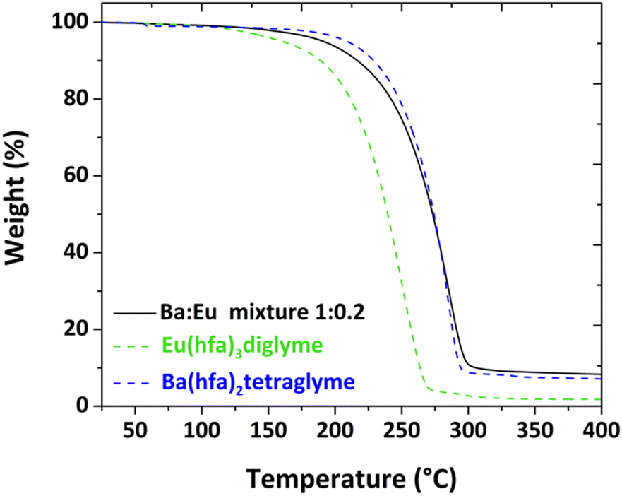 | ||
| Fig. 1 TGA curves of the Ba(hfa)2·tetraglyme and Eu(hfa)3·diglyme single precursors and the Ba(hfa)2·tetraglyme:Eu(hfa)3·diglyme 1:0.2 mixture. | ||
Preliminary deposition studies have been done on silicon substrates to verify the purity, homogeneity, and correct stoichiometry of the films. In order to investigate the influence of temperature on the structure, morphology and DC properties of Eu-doped BaF2 thin films, samples have been fabricated by changing the deposition temperature from 300 to 600 °C. Deposition rates were also estimated from FE-SEM cross-sectional measurements at each temperature. The structural properties of the deposited films were studied by XRD analysis. Fig. 2 illustrates the XRD patterns of Eu-doped BaF2 thin films deposited on silicon substrates at various temperatures and compared with a typical pattern of an undoped BaF2 film deposited at 400 °C.
 | ||
| Fig. 2 XRD patterns of the undoped BaF2 films deposited at 400 °C (black line) on Si and BaF2: Eu (1%) at 300 °C (red line), 350 °C (blue line), 400 °C (yellow line), 500 °C (green line), and 600 °C (purple line) on Si. Graphite has been added as an internal standard. | ||
The diffraction patterns of the analyzed samples show the formation of polycrystalline BaF2 single phase for all the thin films deposited in the 300–600 °C temperature range. In fact, the patterns present diffraction peaks at 2θ values of 25.00°, 28.92°, 41.30°, 48.84°, 51.18°, and 59.82° corresponding, respectively, to the characteristic 111, 200, 220, 311, 222 and 400 reflections of the BaF2 cubic phase (International Centre for Diffraction Data, ICDD, database no. 04-0452). The relative intensities of peaks in these patterns mainly correspond to those reported in the ICDD database, indicating that there is no preferential direction growth. The a-cell parameter for a BaF2 cubic structure was calculated by using graphite as internal standard and the relationship between dhkl and a lattice parameter. In the case of the Eu-doped BaF2 thin films fabricated at different temperatures (300–600 °C), the a-axis cell parameter is 6.16 (7) Å, while for the undoped one the a-axis cell parameter is equal to 6.17 (5) Å. The value of the undoped film is smaller than the theoretical a-axis cell parameter of 6.200 Å (ICDD no. 85-1342), indicating the presence of compressive strain. To our knowledge, no data are available in the literature for the a-axis cell parameter of BaF2 deposited films. The slight reduction of the a lattice parameter for the doped BaF2 samples is due to the introduction, in substitutional positions, of the trivalent Eu3+ ion, which has a smaller ionic radius (1.20 Å in 8-coordination) than the divalent barium ion (1.42 Å in 8-coordination).23
On the other hand, the effect of charge difference between Eu3+ and Ba2+ ions is compensated by the formation of cation vacancies, the formation of fluoride clusters and/or the presence of interstitial fluorine within the structure.44,45 This phenomenon was recently demonstrated by the group of Pellegrino et al. who evaluated the effect of CaF2 structure distortion following the insertion of trivalent Ln ions.21 Therefore, it is expected that an increase of concentration of the dopant ions inside the crystalline structure would produce a shift of the diffraction reflections at even higher 2θ values.
Interestingly, in the present study, the variation of deposition temperature has no evident effect on the diffraction peak positions (Fig. 1), while it can be noted that the peak intensities tend to increase as the deposition temperature is increased, which can be ascribed on the one hand to a higher crystallinity degree, and on the other hand, to an increase of the film thickness up to 500 °C deposition temperature, as also confirmed by the FE-SEM images (see below).
On varying the Eu doping concentrations, as expected, the patterns show a predictable tendency of shifting diffraction peaks to higher values of two theta as the dopant concentration increases.
By extrapolation of the a-axis cell parameter of the doped samples with various amounts of europium, a decreasing trend of the a-axis cell is evident due to the shift of diffraction peaks to higher angles, with values of the parameter going from 6.17(5) for the undoped BaF2 to 6.14 (5) for the 20% doped BaF2 film (Fig. 3). The a-axis cell values of the differently doped films are reported in the table of Fig. 3.
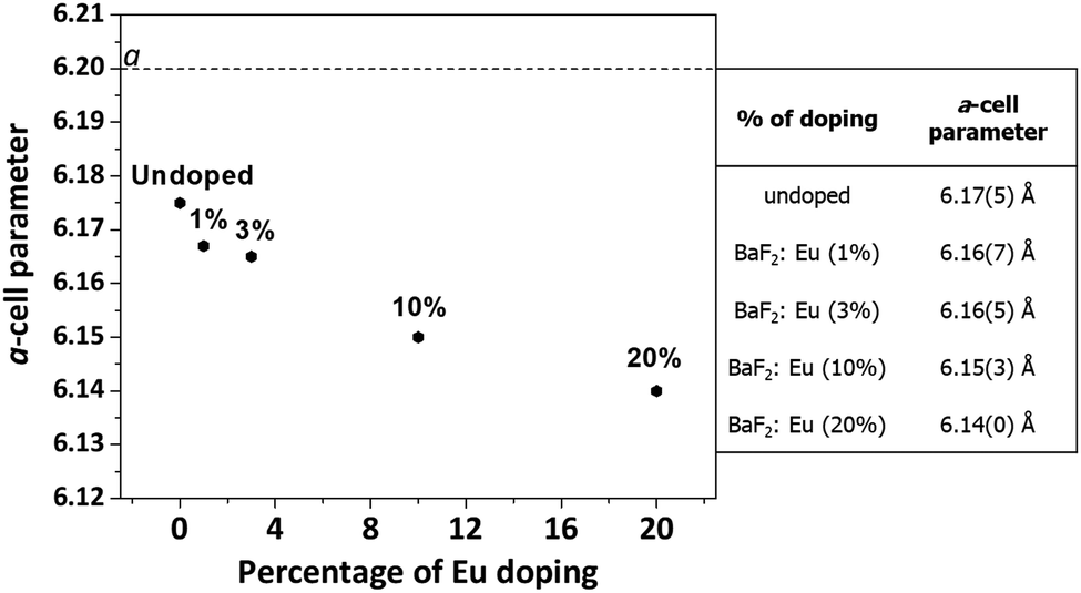 | ||
| Fig. 3 a-axis parameter variation of the BaF2 films as a function of the Eu doping amount. The dotted line indicates the theoretical value of 6.200 Å. | ||
Quantitative EDX analysis has been carried out to establish the composition of the films in terms of Eu3+ ion concentration and to exclude the presence of impurities. Since the percentage of europium (nominal concentration of Eu(hfa)3·diglyme at 1% with respect to Ba(hfa)2·tetraglyme) in the samples is difficult to measure because of the EDX detection limit, additional Eu-doped BaF2 films with a higher concentration of Eu3+ (nominal concentration at 10%) were deposited at 400 °C, in order to evaluate the elemental composition of the film. The EDX spectrum (Fig. S2, ESI†) shows the Ba L lines in the 4.3–5.2 keV range, the F Kα peak at 0.65 keV and the Eu L lines in the 5.5–6.4 keV range. The quantitative analysis confirms a good match between the nominal concentration of the precursor starting mixture, i.e. 0.9 Ba(hfa)2·tetraglyme:0.1 Eu(hfa)3·diglyme, and the EDX quantitative analysis, which yields the following amounts of about 0.9 Ba:0.1 Eu in the film. Furthermore, no O or C peaks are detected (Kα peaks should appear at 0.525 keV and at 0.277 keV, respectively), thus confirming the presence of a pure barium fluoride phase without impurities.
The morphology of the BaF2 thin films was investigated through FE-SEM analysis. The FE-SEM images of Eu-doped BaF2 thin films deposited on Si (100) substrates in the 300–600 °C temperature range are shown in Fig. 4.
 | ||
| Fig. 4 FE-SEM images of BaF2:Eu (1%) films prepared by MOCVD on an Si substrate at deposition temperatures of (a) 300 °C, (b) 400 °C, (c) 500 °C and (d) 600 °C. | ||
For samples deposited at various temperatures, the surfaces look homogeneous and compact over the whole area (1 cm × 1 cm). In Fig. 4(a), the sample deposited at 300 °C presents a very smooth surface with quite small-sized grains, while the films deposited at 400 °C (Fig. 4(b)) present, instead, a compact surface with grains appearing quite irregular in shape and size, of the order of 80 nm. However, when the deposition temperature becomes higher, the grain dimensions increase up to 200–300 nm, as seen in samples deposited at 500 °C (Fig. 4(c)). Furthermore, the sample deposited at the highest temperature of 600 °C (Fig. 4(d)) shows slightly bigger grains up to 400 nm with a well-defined crystalline habit. However, some cracking on the surface is barely visible at this higher temperature. This effect is likely due to the considerable difference between thermal expansion coefficients of the BaF2 film and silicon substrate (BaF2: 18.1 × 10⁻⁶ °C−1vs. Si: 2.6 × 10⁻⁶ °C−1 at 273 K).
Fig. 5 shows a comprehensive overview of cross-sectional images of BaF2: Eu (1%) on films deposited on Si substrates at increasing deposition temperatures. The cross-sections indicate a thickness of 180 ± 30 nm for sample deposited at 300 °C (Fig. 5(a)), 1.93 ± 0.03 μm for films deposited at 400 °C (Fig. 5(b)), 1.91 ± 0.03 μm and 1.43 ± 0.03 μm for samples deposited at 500 °C and 600 °C (Fig. 5(c) and (d)), respectively. Therefore, this behavior points to a clear dependence of film thickness on the deposition temperature. Accordingly, it is possible to calculate the film growth rate (reported in Table S2, ESI†) for films prepared at different temperatures and perform a kinetic study on the MOCVD deposition process of BaF2 films.
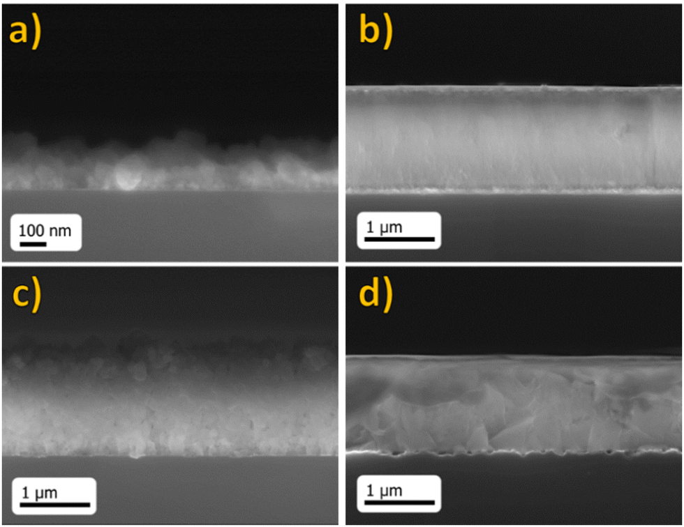 | ||
| Fig. 5 FE-SEM cross-sectional images of Eu-doped BaF2 film on Si at deposition temperatures of (a) 300 °C, (b) 400 °C, (c) 500 °C and (d) 600 °C. | ||
The Arrhenius plot of ln (growth rate) vs. 1000/T for films deposited on Si substrates from 300 °C to 600 °C is shown in Fig. 6. From the Arrhenius plot, two different growth regimes are evident. From 300 °C to 400 °C, the film growth rate increases exponentially with temperature, according to the Arrhenius law. In this temperature range, the BaF2 growth rate is strongly influenced by the substrate temperature and the type of growth is under kinetic control. A growth rate of about 32 nm min−1 is found at 400 °C. Thus, the decomposition of the precursors on the substrate surface can be considered the rate determining step. The activation energy for this first region, calculated from the straight line's slope of Fig. 6, is equal to 77 ± 14 J K−1 mol−1. From 400 °C to 600 °C, instead, a positive slope is derived, from which a negative activation energy is obtained, indicating that, in this deposition temperature range, BaF2 film growth occurs in the mass transport-limited regime, since no dependency of the growth rate on the surface temperature is observed.
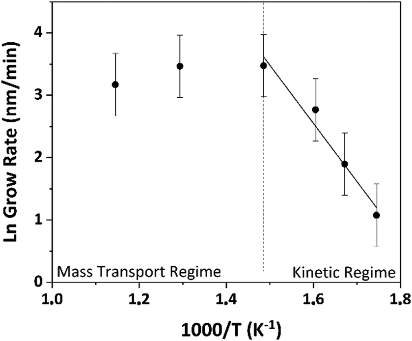 | ||
| Fig. 6 Arrhenius Plot for Eu-doped BaF2 films grown through MOCVD. | ||
Finally, an EDX line mapping investigation has been carried out to assess the vertical compositional homogeneity of the Eu doped BaF2 samples.
The intensities of the Ba L lines and the Eu L lines are remarkably constant throughout the thickness under consideration, as can be observed in Fig. 7 for the 20% Eu-doped sample. This indicates that there is no stratification or segregation of the doping element in the film, thus confirming a compositional homogeneity both on the surface and along the entire thickness of the film.
 | ||
| Fig. 7 EDX line mapping of the BaF2:Eu (20%) cross-sectional sample. | ||
As a representative example, the room temperature excitation spectrum of the Eu3+ doped BaF2 thin film prepared at 600 °C is shown in Fig. 8. The excitation bands are typical of the Eu3+ ion, in good agreement with those found for similar fluoride hosts.46 In particular, the spectrum is dominated by a quite narrow excitation band peaked at 394 nm, due to the 7F0 → 5L6 transition of the Eu3+ ion. Moreover, other less intense bands are present in the spectrum, due to transitions from the ground state to several excited energy levels of the Eu3+ ions.
 | ||
| Fig. 8 Black line: room temperature excitation spectrum (λem = 613 nm) of the Eu3+ doped BaF2 thin film grown at 600 °C. The energy levels involved in the transitions are indicated as 7F0→ 5D4 (1), 5G2–6 (2), 5L6 (3), 5D3 (4), 5D2 (5), 5D1 (6); and 7F1 → 5D1 (7). Red line: emission spectrum of the used UV LED lamp. | ||
It is worth noting that a weak band around 530 nm is present, due to the 7F1 → 5D1 transition.
In fact, the population of the 7F1 energy level (N1) from which this transition starts, can be obtained according to the Boltzmann distribution law:
 | (1) |
From the excitation spectrum shown in Fig. 8, the 7F0 → 5D1 and 7F1 → 5D1 excitation bands have been fitted with Gaussian profiles and their barycenters are found to be at 523.4 ± 0.2 nm (19106 ± 7 cm−1) and 531.5 ± 0.5 nm (18815 ± 17 cm−1), respectively. Therefore, the energy gap between the 7F0 and 7F1 energy levels is estimated to be 290 ± 30 cm−1. For this energy gap, assuming that the population of the 7F2 energy level is negligible at room temperature with respect to the sum of 7F0 and 7F1 energy level populations, from eqn (1) the 7F1/7F0 population ratio is found to be 0.25 at room temperature, indicating that if the laser radiation is properly tuned, transitions starting from the 7F1 level are possible and can contribute to populate the 5DJ excited energy levels. Moreover, in Fig. 8 the emission spectrum of the used UV LED flashlight has been shown (red line).
By comparing the Eu3+ ion excitation spectrum and the emission spectrum of the flashlight, it can be noted that the exciting source can be considered as multi-wavelength radiation, able to efficiently excite the Eu3+ ions. In fact, from Fig. 8, it can be noted that the stronger Eu3+ excitation bands, indicated as (2) and (3) in Fig. 8, are located in the near UV region from 350 to 400 nm, well inside the radiation emitted from our LED flashlight.
The luminescence spectra of Eu-doped BaF2 thin films grown at different temperatures are shown in Fig. 9. The emission bands are due to transitions of the Eu3+ ions, decaying radiatively from the 5D0 excited level to the lower lying 7FJ (J = 0, 1, 2, 3, 4) ones.
 | ||
| Fig. 9 Room temperature emission spectra of Eu doped (1%) BaF2 thin films (λexc = 385 nm) on Si (100) support, at different deposition temperatures: (a) 600 °C; (b) 500 °C; (c) 400 °C; (d) 350 °C; and (e) 300 °C. Transition assignments for emission bands: (1) 5D1 → 7F2; (2) 5D0 → 7F0; (3) 5D0 → 7F1; (4) 5D0 → 7F2; (5) 5D0 → 7F3; and (6) 5D0 → 7F4. Energy transitions calculated for Eu3+ ions in C3v (black bars) and Oh (red bars) local symmetry (from ref. 47 and 48). | ||
All the samples show excellent emission intensities, as demonstrated by the observed high signal to noise ratios.
For the sake of clarity, the energy level schemes of Eu3+ ions in the BaF2 host, in Oh and C3v symmetry sites, have been shown in Fig. 10, taken from Jouart et al.47,48
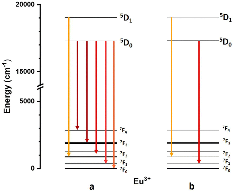 | ||
| Fig. 10 Energy level schemes of Eu3+ ions in the BaF2 host, in C3v (a) and Oh (b) symmetry sites (from ref. 47 and 48). Arrows represents the observed emission transitions. | ||
From the emission spectra, it can be noted that the features of the emission bands are different on changing the deposition temperature. Of great significance are the emission bands in the 580–600 nm (17240–16667 cm−1) range, due to 5D0 → 7F1 magnetic dipole transitions that are poorly dependent on the local environment around the lanthanide ions.49 Differently, the bands in the 610–630 nm (16393–15873 cm−1) region are due to 5D0 → 7F2 electric dipole transitions that are allowed only for lanthanide sites without inversion symmetry, and they are very sensitive to local symmetry.
The asymmetry ratio R, defined as
 | (2) |
From the observed emission spectra, it is clear that for the sample deposited at 300 °C (see Fig. 9(e)) the intensity ratio of the two emission bands in the 610–630 nm (16393–15873 cm−1) and 580–600 nm (17240–16667 cm−1) range, due to the 5D0 → 7F2 and 5D0 → 7F1 transitions, respectively, is much higher (around 2) than those observed for the emission spectra for samples deposited at higher temperatures, for which R is less than 1.3 (see Fig. 9(a)–(d)).
Interestingly, this behavior suggests that, on average, the Eu3+ ions in the BaF2 sample deposited at 300 °C are in a less symmetric environment, which is compatible with a slightly lower crystallinity degree with respect to other samples prepared at higher temperatures.
These results are also in agreement with those found from the XRD analysis (Fig. 2). The lower symmetry for the sample prepared at the lowest temperature could therefore be due to a higher number of defects, and this observation indicates that the defect amount decreases in the lattice structure with increasing deposition temperature, due to the higher crystallinity degree. This behavior agrees with the results obtained by Sharma et al., who investigated the spectroscopic properties of Eu3+ doped BaF2 nanoparticles13 heat treated at different temperatures (from 400 to 800 °C) and found that the Eu3+ ions are in a more asymmetric environment in the sample treated at lower temperatures.
The specific nature of the sites in which the Eu3+ ions are accommodated was investigated through site-selective laser spectroscopy.47,48 Generally, Eu3+ in doped fluorite-type crystals is located in cubic sites with Oh symmetry, i.e. with a bivalent cation being replaced and a charge-compensating F− ion distant from the Eu3+, (see Fig. S3a, ESI†) which is the case for BaF2 when co-doped with a small amount of NaF.53
Additionally, a trigonal site with C3v symmetry has been identified,47,51 where a compensating F− ion is located in the (½, ½, ½) next-nearest-neighbor (NNN) interstitial position (see Fig. S3b, ESI†). This arrangement causes the energy levels of the lanthanide ions to split into several components, in particular in two components for both the 7F1 and 7F2 multiplets, which is the most common situation for very low Eu3+ concentrations in the BaF2 host (0.03 mol%).42 For higher Eu3+ concentrations (around 1 mol%) other emission lines were also observed, attributed to different local environments of the lanthanide, tentatively also proposed for pairs of nearest neighbors (NN) or NNN Eu3+ ions.
To corroborate these findings, we conducted ab initio multireference SA-CASSCF calculations on Eu-doped BaF2 models featuring Oh and C3v symmetry (see Fig. S3c and d, respectively, ESI†). Remarkably, such models are strongly ionic due to the presence of several unbalanced F− anions, but this should not influence the energy levels of Eu3+ in a considerable way, while the coordination around the lanthanide does.52,53 Evaluation of the 7FJ (J = 0–6) energies in the two cases, compared with the available experimental data from Jouart et al.,47,48 is reported in Table 1. The calculated energies follow the trend of the experimental data, showing a good agreement (i.e., within ±100 cm−1) in all cases but the 7F2 levels, for which the discrepancy is up to almost 200 cm−1. Some information on the location of Eu3+ ions can also be inferred from the profile detail of the emission bands of the measured spectra. As a general observation, the emissions starting from the different Stark levels are strongly overlapped, mainly due to homogeneous (i.e., thermal) and inhomogeneous (i.e., local disorder around the lanthanide ion) broadening. The good agreement between the theoretical and experimental data of the 7FJ level energies makes it possible to compare the presently observed transitions with those previously reported by Jouart et al. in relation to different sites.47,48 To clearly show the presence of Eu3+ in different sites in our samples, in Fig. 9 we report, along with the emission spectra, the 5D0 → 7FJ (J = 0–5) and 5D1 → 7F2 transition energies taken from the literature,47 with black and red bars referring to transitions between energy levels in trigonal (C3v) and cubic (Oh) symmetry, respectively. To do this, we analyzed the emission bands due to the 5D0 → 7F1 magnetic dipole transition, for which emission contributions deriving from Eu3+ ions accommodated both in C3v and Oh sites are expected.
| O h | C 3v | |||||||
|---|---|---|---|---|---|---|---|---|
| Exp48 | Th | n | Δ | Exp47 | Th | n | Δ | |
| 7F0 | 0 | 0.0 | 1 | 0 | 0 | 1 | ||
| 7F1 | 348 | 366.1 | 3 | −18.1 | 327 | 343.7 | 2 | −16.7 |
| 392 | 414.8 | 1 | −22.8 | |||||
| 7F2 | 869 | 990.6 | 3 | −121.6 | 859 | 977.5 | 2 | −118.5 |
| 1283 | 1087.7 | 2 | 195.3 | 884 | 1014.9 | 1 | −130.9 | |
| 1290 | 1094.2 | 2 | 195.8 | |||||
| 7F3 | 1865 | 1899.5 | 3 | −34.5 | 1845 | 1890.8 | 2 | −45.8 |
| 1938 | 1902.0 | 3 | 19.3 | 1877 | 1906.1 | 2 | −29.1 | |
| 1968.7 | 1 | 1924 | 1910.9 | 2 | 13.1 | |||
| 1950 | 1974.1 | 1 | −24.1 | |||||
| 7F4 | 2857 | 2765.7 | 1 | 2850 | 2767.7 | 1 | 82.3 | |
| 2902.4 | 3 | 2869 | 2900.7 | 1 | ||||
| 2970.2 | 3 | −74.3 | 2906.4 | 2 | ||||
| 2999.3 | 2 | 2967.5 | 1 | −85.8 | ||||
| 2975.7 | 2 | |||||||
| 3003.2 | 2 | |||||||
| 7F5 | — | 3970.3 | 3 | 3789 | 3969.6 | 3 | ||
| 4038.8 | 3 | 4035.7 | 2 | |||||
| 4101.5 | 2 | 4041.2 | 1 | |||||
| 4102.3 | 3 | 4083.9 | 1 | |||||
| 4106.6 | 2 | |||||||
| 4125.8 | 2 | |||||||
| 7F6 | — | 5184.0 | 1 | — | 5149.6 | 1 | ||
| 5197.8 | 3 | 5163.9 | 2 | |||||
| 5205.4 | 3 | 5196.1 | 2 | |||||
| 5277.2 | 2 | 5230.7 | 1 | |||||
| 5279.4 | 3 | 5238.4 | 1 | |||||
| 5283.7 | 1 | 5284.4 | 2 | |||||
| 5298.2 | 2 | |||||||
| 5304.6 | 1 | |||||||
| 5306.8 | 1 | |||||||
In this case, the two expected 5D0 → 7F1 transitions for Eu3+ ions in BaF2 in the C3v symmetry site found by Jouart et al.47 and peaked at 16975 and 16910 cm−1, at a measurement temperature of 77 K, are in very good agreement with our measurements, thus suggesting that contributions from the Eu3+ ions in C3v symmetry is remarkable for our samples. On the other hand, energy gaps of 17304 cm−1 and 16956 cm−1 between the 5D0 and 7F0 or 7F1 Stark energy sublevels of Eu3+ ions in cubic center (Oh),48 respectively, have been estimated, which were hardly recognized in the present investigation. Thus, the latter contribution to the 5D0 → 7F1 emission transitions is probably low, since the respective band (around 16700–17200 cm−1) shows a very broad profile without prominent features. Moreover, it should be underlined that the emission spectra could also feature contributions from Eu3+ ions located in other sites47 and/or from vibronic transitions, particularly important at room temperature,54 as well as bands derived from Eu3+ clustering, i.e. pairs of NN or NNN Eu3+ ions, as observed in doped CaF255 and BaF2 hosts.56 Remarkably, a weak but clearly detected emission band is observed at 562.4 ± 0.3 nm (17781 ± 9 cm−1), attributed to a transition between the 5D1 and 7F2 levels of the Eu3+ ions. Notably, the wavelength position of this band is in perfect agreement with that by Jouart et al.47 (562.7 nm, 17771 cm−1), assigned to a transition of Eu3+ ions in a C3v center. From the emission spectra, it can be noted that the intensity of this band increases on increasing the deposition temperature. Since the 5D1 emission is strongly quenched by cross-relaxation processes between two Eu3+ ions47 the observed behavior suggests the presence of clustering of the Eu3+ ions for samples prepared at the lowest temperature. On increasing the deposition temperature, the emission intensity of the band from the 5D1 level increases, indicating that the Eu3+ ions tend to separate, therefore decreasing the cross-relaxation processes.
In order to gain more information about the sites where the Eu3+ ions are accommodated, room temperature emission decay curves were also measured for the Eu doped (1%) BaF2 thin film sample deposited at 600 °C on Si (100) by monitoring emissions at 612 nm (16340 cm−1) and at 589 nm (16978 cm−1), attributed to 5D0 → 7F2 and 5D0 → 7F1 transitions, respectively. The measured emission decay curves are shown in Fig. 11.
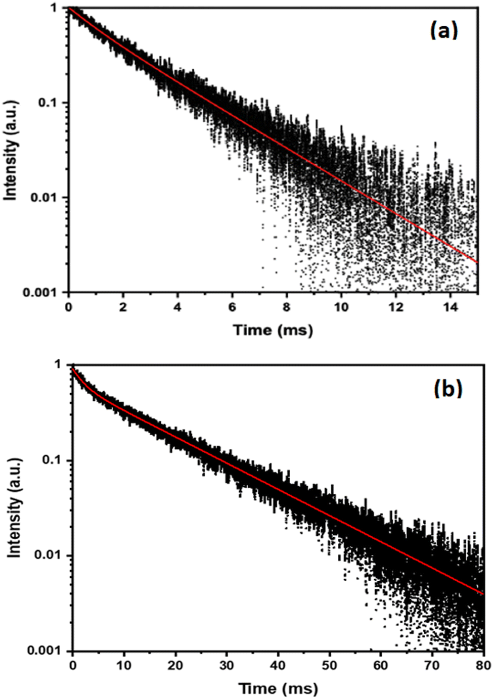 | ||
| Fig. 11 Room temperature emission decays of Eu doped (1%) BaF2 thin films (λexc = 532 nm) on the Si (100) support, at 600 °C deposition temperature: (a) λem = 612 nm, 5D0 → 7F2 transition and (b) λem = 589 nm, 5D0 → 7F1 transition. | ||
The emission decays were fitted using a multiexponential curve, defined as:
 | (3) |
The intensity-weighted average lifetime τavg is defined as:57
 | (4) |
The emission decays measured at 612 and 589 nm were fitted with a biexponential curve (see eqn (3)) and the values of weights, decay times and intensity-weighted average lifetime are reported in Table 2. It is worth noting that the obtained τavg value, 2.36 ms, for the emission at 612 nm (due to the 5D0 → 7F2 transition) is similar to the value (1.80 ms) found at room temperature from the same emission wavelength by Wang et al.58 for Eu3+ doped BaF2 microcrystals, prepared by a hydrothermal technique. Of notable interest, the τavg value obtained in the present investigation for the emission at 589 nm (due to the 5D0 → 7F1 transition) is much longer than the value found for the 612 emission (see Table 2). This behavior indicates that contributions to the emission intensity from different sites are present in the decay curves. In fact, this indicates that Eu3+ sites with relatively high symmetry, probably close to cubic, can generate emission intensity mainly around 589 nm, as highly symmetric sites allow mainly 5D0 → 7F1 magnetic dipole transitions. Moreover, these highly symmetric sites do not contribute to the emission at a wavelength around 612 nm, as for them the 5D0 → 7F2 electric dipole transitions are almost completely forbidden. The τavg value found at room temperature in the present study for emission at 589 nm, which is 15.03 ms, is much longer than those found by other authors for the same fluoride nanocrystals in different systems, as nanocrystalline BaF2:Eu3+ glass-ceramic materials,59 with an average lifetime of around 3.4 ms, or Eu3+ doped nanoparticles prepared by the ionic liquid-assisted solvothermal method,13 with average lifetimes depending on the experimental conditions, ranging from 1.15 to 5.61 ms at room temperature. This behavior suggests that for the sample deposited at the highest temperature (600 °C) a significant fraction of the luminescent Eu3+ ions are accommodated in sites with high symmetry, tentatively attributed to site close to cubic symmetry (see Fig. S3, ESI†). Nonetheless, other experimental evidence involving site selection spectroscopy would be needed to confirm this hypothesis, but this is outside of the scope of this study.
| Emission wavelength (nm) | τ 1 (ms) | A 1 | τ 2 (ms) | A 2 | τ avg (ms) |
|---|---|---|---|---|---|
| 612 nm | 0.97 ± 0.03 | 22% ± 2% | 2.520 ± 0.015 | 78% ± 2% | 2.36 ± 0.03 |
| 589 nm | 2.073 ± 0.015 | 31.6% ± 0.1% | 15.81 ± 0.02 | 68.4% ± 0.1% | 15.03± 0.02 |
Conclusions
An extensive study has been conducted on the production of europium doped BaF2 thin films for use in energy conversion. In order to have an easily scalable process and strong control over the composition, microstructure, and morphology of the films, an MOCVD approach is proposed. The chemical composition of the films has been tuned by changing the composition of the precursor mixture in order to tailor the useful Eu amount to optimize the luminescence properties. The diffraction patterns show that polycrystalline BaF2 phase films are produced in the 300 to 600 °C temperature range, with peak intensities that tend to increase with the increasing deposition temperature. These phenomena can be attributed to both an increase in film thickness and a higher degree of crystallinity. Additionally, the peak positions are strictly related to the dopant %, with a shift toward higher angle with increasing Eu3+ ion concentrations, thus resulting in a decrease of the lattice parameter, an effect due to the replacement of larger Ba2+ ions by the smaller Eu3+ ions. The morphology, investigated through FE-SEM analysis is impacted by temperature, particularly as the deposition temperature increases, grain dimension tends to rise up until 400 nm, as it is observed in samples deposited at 600 °C. Film growth rates as high as 32 nm min−1 have been found in the deposition range of 400–500 °C.The prepared thin films show a strong Stokes luminescence under excitation in the excited levels of Eu3+ ions. The profile of the emission bands depends on the deposition temperature, indicating that the local environment of the lanthanide ions is slightly different. The sample prepared at the lowest temperature reveals that the Eu3+ ions are accommodated in sites of lower symmetry with respect to the samples prepared at other temperatures, most probably due to a higher number of defects. The defect amount decreases in the lattice structure with increasing deposition temperature. Analysis of the emission decay curves reveals that a relevant number of Eu3+ ions with quite high symmetry is present. The simulation of the energy levels of the 7FJ (J = 0–6) multiplets for the Eu3+ ions in different site geometries, calculated by CASSCF methods, indicates that the calculated energy levels agree with those extracted from experimental data.
These MOCVD grown Eu-doped BaF2 films are very promising for applications as downshifting layers in photovoltaic cells to exploit the UV component of the solar spectrum.
Conflicts of interest
There are no conflicts to declare.Acknowledgements
This work has been partially funded by the European Union (NextGeneration EU), through the MUR-PNRR project SAMOTHRACE (ECS00000022). A. S. thanks the University of Verona, Verona, Italy, for funding in the framework of the “Joint Research 2022”. A. L. Pellegrino and E. Radicchi thank the Ministero dell’Università e della Ricerca within the PON “Ricerca e Innovazione” 2014–2020 Azioni IV.4 program. The authors thank Francesco Mazzer, Treviso, Italy, and Claudia Mezzalira, Nanomnia, Viale Archimede, 25, Campagnola di Zevio, Verona, Italy, for expert technical assistance. The authors thank the Bionanotech Research and Innovation Tower (BRIT) Laboratory of University of Catania (Grant no. PONa3_00136 financed by the Italian Ministry for Education, University and Research, MIUR) for the diffractometer facility. The authors gratefully acknowledge the Technological Platform Center of the University of Verona, Italy, for use of optical experimental setups. The authors also acknowledge the Computational Platform of the Information Systems and Technology Direction of the University of Verona, Italy.Notes and references
- G. W. Crabtree and N. S. Lewis, Phys. Today, 2007, 60, 37–42 CrossRef CAS.
- NREL. Best Research-Cell Efficiency. (2020).
- X. Huang, S. Han, W. Huang and X. Liu, Chem. Soc. Rev., 2013, 42, 173–201 RSC.
- D. Yang, H. Liang, Y. Liu, M. Hou, L. Kan, Y. Yang and Z. Zanga, Dalton Trans., 2020, 49, 4725–4731 RSC.
- H. T. Kim, K. Lee, W. Jin, H. D. Um, M. Lee, E. Hwang, T. H. Kwon and K. Seo, Sci. Rep., 2018, 8, 16974 CrossRef PubMed.
- J. C. Bünzli and A. S. Chauvin, Chapter 261 – Lanthanides in Solar Energy Conversion. in Including Actinides, Elservier, 2014, vol. 44, pp. 169–281 Search PubMed.
- J. C. G. Bünzli and S. V. Eliseeva, Chem. Sci., 2013, 4, 1939–1949 RSC.
- G. Lucchini, A. Speghini, P. Canton, F. Vetrone and M. Quintanilla, Nanoscale Adv., 2019, 1, 757 RSC.
- N. Kumam, L. P. Singh, K. Srivastava and N. R. Singh, J. Lumin., 2018, 203, 59–66 CrossRef CAS.
- N. U. Rahman, W. U. Khan, S. Khan, X. Chen, J. Khan, J. Zhao, Z. Yang, M. Wu and Z. Chi, J. Mater. Chem. A, 2019, 7, 6467–6474 RSC.
- M. Ran, N. Liu, H. Y. Yang, R. Meng, M. Chen, H. Lu and Y. Yang, Appl. Phys. Lett., 2020, 116, 113503 CrossRef CAS.
- R. N. Grass and W. J. Stark, Chem. Commun., 2005, 1767–1769 RSC.
- R. K. Sharma, S. Nigam, Y. N. Chouryal, S. Nema, S. P. Bera, Y. Bhargava and P. Ghosh, ACS Appl. Nano Mater., 2019, 2, 927–936 CrossRef CAS.
- E. Palo, L. Pihlgren, M. Tuomisto, T. Laihinen, I. Hyppanen, J. Kankare, M. Lastusaari, T. Soukka, H. C. Swart and J. Holsa, Opt. Mater., 2016, 59, 49–54 CrossRef CAS.
- V. Kale, M. Lastusaari, J. Holsa and T. Soukka, RSC Adv., 2015, 5, 35858–35865 RSC.
- M. R. Catalano, A. L. Pellegrino, P. Rossi, P. Paoli, P. Cortelletti, M. Pedroni, A. Speghini and G. Malandrino, New J. Chem., 2017, 41, 4771–4775 RSC.
- A. L. Pellegrino, M. R. Catalano, P. Cortelletti, G. Lucchini, A. Speghini and G. Malandrino, Photochem. Photobiol. Sci., 2018, 17, 1239–1246 CrossRef CAS PubMed.
- X. Zhang, Z. Zhao, X. Zhang, D. B. Cordes, B. Weeks, B. Qiu, K. Madanan, D. Sardar and J. Chaudhur, Nano Res., 2015, 8, 636–648 CrossRef CAS.
- A. L. Pellegrino, P. Cortelletti, M. Pedroni, A. Speghini and G. Malandrino, Adv. Mater. Interfaces, 2017, 4, 1–6 Search PubMed.
- A. L. Pellegrino, G. Lucchini, A. Speghini and G. Malandrino, J. Mater. Res., 2020, 35, 2950–2966 CrossRef CAS.
- A. L. Pellegrino, S. La Manna, A. Bartasyte, P. Cortelletti, G. Lucchini, A. Speghini and G. Malandrino, J. Mater. Chem. C, 2020, 8, 3865–3877 RSC.
- S. Balabhadra, M. F. Reid, V. Golovko and J. R. Wells, J. Alloys Compd., 2020, 834, 155165 CrossRef CAS.
- E. I. Madirov, V. A. Konyushkin, A. N. Nakladov, P. P. Fedorov, T. Bergfeldt, D. Busko, I. A. Howard, B. S. Richards, S. V. Kuznetsov and A. Turshatov, J. Mater. Chem. C, 2021, 9, 3493–3503 RSC.
- J. R. Wells and R. J. Reeves, J. Lumin., 1996, 66–67, 219–223 Search PubMed.
- W. Drozdowski and A. J. Wojtowicz, J. Alloys Compd., 2000, 300–301, 261–266 CrossRef CAS.
- M. Heise, G. Scholz, T. Krahl and E. Kemnitz, Solid State Sci., 2019, 91, 113–118 CrossRef CAS.
- B. Ritter, P. Haida, F. Fink, T. Krahl, K. Gawlitza, K. Rurack, G. Scholz and E. Kemnitz, Dalton Trans., 2017, 46, 2925–2936 RSC.
- C. Lorbeer, J. Cybinska, E. Zych and A.-V. Mudring, Opt. Mater., 2011, 34, 336–340 CrossRef CAS.
- I. G. Neizvestny, D. V. Ishchenko, I. O. Akhundov, S. P. Suprun and O. E. Tereshchenko, Dokl. Phys., 2020, 65, 15–17 CrossRef CAS.
- X. M. Fang, T. Chatterjee and P. J. McCann, J. Vac. Sci. Technol., B, 1996, 14, 2267–2270 CrossRef CAS.
- P. S. Kirlin, R. Binder, D. R. Winn, J. O'Hare, C. LaPierre and M. Whitmore, Nucl. Instrum. Methods Phys. Res., Sect. A, 1990, 289, 261–264 CrossRef.
- M. L. Hitchman, S. H. Shamlian, D. D. Gilliland, D. J. Cole-Hamilton, J. A. P. Nash, S. C. Thompson and S. L. Cook, J. Mater. Chem., 1995, 5, 47–52 RSC.
- A. P. Purdy, A. D. Berry, R. T. Holm, M. Fatemi and D. K. Gaskill, Inorg. Chem., 1989, 28, 2799–2803 CrossRef CAS.
- H. Sato and S. Sugawara, Inorg. Chem., 1993, 32, 1941–1945 CrossRef CAS.
- G. Malandrino, F. Castelli and I. L. Fragalà, Inorg. Chim. Acta, 1994, 224, 203–207 CrossRef CAS.
- G. Malandrino and I. L. Fragalà, Coord. Chem. Rev., 2006, 250, 1605–1620 CrossRef CAS.
- F. Neese, Wiley Interdiscip. Rev.: Comput. Mol. Sci., 2012, 2, 73–78 CAS.
- F. Neese, Wiley Interdiscip. Rev.: Comput. Mol. Sci., 2022, 12, e1606 Search PubMed.
- F. Neese, F. Wennmohs, U. Becker and C. Riplinger, J. Chem. Phys., 2020, 152(22), 224108 CrossRef CAS PubMed.
- H. E. Swanson and E. Tatge, Standard X-ray diffraction powder patterns, National Bureau of Standards Circular (U.S.), Circular, 1953, 539(1), 1–95 Search PubMed.
- D. Aravena, F. Neese and D. A. Pantazis, J. Chem. Theory Comput., 2016, 12(3), 1148–1156 CrossRef CAS PubMed.
- F. Weigend and R. Ahlrichs, Phys. Chem. Chem. Phys., 2005, 7, 3297–3305 RSC.
- M. Kaupp, P. v R. Schleyer, H. Stoll and H. Preuss, J. Chem. Phys., 1991, 94(2), 1360–1366 CrossRef CAS.
- F. Ma, F. Su, R. Zhou, Y. Ou, L. Xie, C. Liu, D. Jiang, Z. Zhang, Q. Wu, L. Su and H. Liang, Mater. Res. Bull., 2020, 125, 110788 CrossRef CAS.
- D. Chen and Y. Wang, Nanoscale, 2013, 5, 4621–4637 RSC.
- P. Cortelletti, M. Pedroni, F. Boschi, S. Pin, P. Ghigna, P. Canton, F. Vetrone and A. Speghini, Cryst. Growth Des., 2018, 18, 686–694 CrossRef CAS.
- J. P. Jouart, C. Bissieux and G. Mary, J. Lumin., 1987, 37(3), 159–165 CrossRef CAS.
- J. P. Jouart, M. Bouffard, G. Klein and G. Mary, J. Lumin., 1991, 50(5), 273–277 CrossRef CAS.
- R. D. Peacock, The intensities of lanthanide f ↔ f transitions, Rare Earths. Structure and Bonding, Springer, Berlin, Heidelberg, 1975, p. 22 Search PubMed.
- A. M. Srivastava, M. G. Brik, W. W. Beers and W. Cohen, Opt. Mater., 2021, 110931 CrossRef CAS.
- J. P. R. Wells, Laser spectroscopy of alkaline earth fluoride crystals doped with trivalent samarium and europium ions, University of Canterbury. Physics and Astronomy, 1996 Search PubMed.
- D. Aravena, M. Atanasov and F. Neese, Inorg. Chem., 2016, 55(9), 4457–4469 CrossRef CAS PubMed.
- L. Babetto, S. Carlotto, A. Carlotto, M. Rancan, G. Bottaro, L. Armelao and M. Casarin, Inorg. Chem., 2021, 60(1), 315–324 CrossRef CAS PubMed.
- P. A. Tanner, Chem. Soc. Rev., 2013, 42, 5090 RSC.
- S. Renard, P. Camy, A. Braud, J. L. Doualan and R. Moncorgé, J. Alloys Compd., 2008, 451(1–2), 71–73 CrossRef CAS.
- E. I. Madirov, V. A. Konyushkin, A. N. Nakladov, P. P. Fedorov, T. Bergfeldt, D. Busko, I. A. Howard, B. S. Richards, S. V. Kuznetsov and A. Turshatov, J. Mater. Chem. C, 2021, 9, 3493 RSC.
- Y. Li, S. Natakorn, Y. Chen, M. Safar, M. Cunningham, J. Tian and D. D. Li, Front. Phys., 2020, 8, 576862 CrossRef.
- X. Wang, Y. Bu, Y. Xiao, C. Kan, D. Lu and X. Yan, J. Mater. Chem. C, 2013, 1, 3158–3166 RSC.
- N. Pawlik, B. Szpikowska-Sroka, J. Pisarska, T. Goryczka and W. A. Pisarski, Materials, 2019, 12, 3735 CrossRef CAS PubMed.
Footnote |
| † Electronic supplementary information (ESI) available. See DOI: https://doi.org/10.1039/d3tc02666c |
| This journal is © The Royal Society of Chemistry 2023 |