
 Open Access Article
 This Open Access Article is licensed under a
 Creative Commons Attribution 3.0 Unported Licence
High gain complementary inverters based on comparably-sized IGZO and DNTT source-gated transistors
Eva
Bestelink
 a,
Pongsakorn
Sihapitak
ab,
Ute
Zschieschang
c,
Leslie
Askew
a,
John M.
Shannon
a,
Juan Paolo
Bermundo
b,
Yukiharu
Uraoka
b,
Hagen
Klauk
c and
Radu A.
Sporea
*a
a,
Pongsakorn
Sihapitak
ab,
Ute
Zschieschang
c,
Leslie
Askew
a,
John M.
Shannon
a,
Juan Paolo
Bermundo
b,
Yukiharu
Uraoka
b,
Hagen
Klauk
c and
Radu A.
Sporea
*a
aAdvanced Technology Institute, School of Computer Science and Electronic Engineering, Faculty of Engineering and Physical Sciences, University of Surrey, Guildford, Surrey, GU2 7XH, UK. E-mail: r.a.sporea@surrey.ac.uk
bDivision of Materials Science, Nara Institute of Science and Technology, 8916-5 Takayama, Ikoma, Nara 630-0192, Japan
cMax Planck Institute for Solid State Research, 70569 Stuttgart, Germany
First published on 8th August 2023
Abstract
We report the first implementation of a complementary circuit using thin-film source-gated transistors (SGTs). The n-channel and p-channel SGTs were fabricated using the inorganic and organic semiconductors amorphous InGaZnO (IGZO) and dinaphtho[2,3-b:2′,3′-f]thieno[3,2-b]thiophene (DNTT), respectively. The SGTs exhibit flat output characteristics and early saturation (dVDSAT/dVGS = 0.2 and 0.3, respectively), even in the absence of lateral field-relief structures, thanks to the rectifying source contacts realized with Pt and Ni, respectively. Hence, the complementary inverter shows excellent small-signal gain of 368 V V−1 and noise margin exceeding 94% of the theoretical maximum. We show that the trip point of such inverters can be tuned optically, with interesting applications in compact detectors and sensors. Numerical simulation, using Silvaco ATLAS, reveals that optimized and monolithically-integrated SGT-based complementary inverters may reach a small-signal gain over 9000 V V−1, making them highly suited to low and moderate speed digital thin-film applications. This proof-of-concept demonstration provides encouraging results for further integration and circuit level optimizations.
Introduction
Traditionally used in display panels, thin-film transistor (TFT) circuits are expanding to cover a wide range of applications.1–6 While current density, cut-off frequency and transconductance are important for driving large loads at high frequencies, properties such as: stability under electrical, thermal, and optical stress; ease of fabrication with good performance uniformity; and cost of production over large areas are important for viable commercial application.7,8Metal oxide semiconductors show great potential for future analog and digital applications due to their high electrical performance, comparatively low-cost fabrication and ability to easily tune their properties via material composition and processing.5,9,10 Such materials offer predominantly unipolar carrier transport, with one of the most widely adopted, indium–gallium–zinc oxide (IGZO), operating with electron conduction.11 Hole-conducting oxides are being actively researched and recent progress focuses on simultaneously obtaining high charge-carrier mobility and an adequate on/off current ratio.12
This is important because, for complementary digital logic circuits, a large mismatch in carrier mobility and thus on-current density needs to be compensated by proportional sizing of the respective transistors,13 which in some cases can be quite extreme. Device stability and off-current-related challenges in p-channel amorphous oxides have been persistent and are still hampering development of commercial applications.9,12,14
Ideally, complementary logic would be used, as opposed to unipolar circuits, because of the compact footprint and the negligible standby power dissipation.13 Thus, it is favorable to attempt to create n- and p-channel transistors with closely matched on-state current density. A comprehensive review by Nomura15 covers the design considerations, as well as various implementations of complementary inverters. The highest small-signal gain obtained by the complementary inverters reviewed produced a value up to 123 V V−1 at a supply voltage of 10 V and with a power consumption of 9.8 μW.16 This result was obtained using p-channel TFTs based on semiconducting carbon nanotubes (CNTs). Although CNT-based technologies are attractive for their high performance, the associated safety and toxicity concerns17 render them less favorable than many alternatives.
Organic semiconductors have a long history of development, with a majority of available materials showing hole conduction. A wide selection of materials with relatively high mobilities are available, and, even as the current density is not quite on par with that of InGaZnO (IGZO) transistors, complementary logic circuits have been successfully demonstrated.15 Inverters with ZnO n-channel and pentacene p-channel TFTs are capable of delivering a gain of around 100 V V−1 at VDD = 7 V and a much lower power consumption of 0.7 nW.18 Another typical implementation demonstrated complementary inverters based on In2O3/ZnO heterostructure n-channel TFTs with small molecule 2,7-dioctyl[1]-benzothieno[3,2-b][1]benzothiophene (C8-BTBT) and polymer indaceno-dithiophene-benzothiadiazole (C16IDT-BT) blend p-channel TFTs. The inverters produced a small-signal gain of 30 V V−1 at supply voltage VDD = 60 V.19 These results were obtained with devices that required relatively large footprints (W/L = 500/90 μm and 500/90 μm for the former n- and p-channel devices, while W/L = 1000/80 μm and 1000/50 μm interdigitated channel for the latter).
Here, we show a proof of concept realization of complementary logic operation using n-channel (IGZO-based) and p-channel (dinaphtho[2,3-b:2′,3′-f]thieno[3,2-b]thiophene20(DNTT)-based) transistors realized using vacuum processing in a source-gated transistor (SGT)21,22 architecture. The advantage of our approach is that the transistors display high intrinsic gain and low-voltage saturation, promoting a sharp logic transition with good noise margin in a complementary inverter configuration,23 with very small standby-power dissipation.24 In principle, the channel length could also be reduced significantly without suffering from deleterious scaling effects.25,26 Highly pertinent to digital logic applications, by relying on the contact barrier introduced at the source electrode to tailor the current density, the two transistors show similar on-current levels, which permits close to equal sizing in the circuit layout.
To our knowledge, this is the first report of a source-gated transistor-based complementary inverter. The circuit shows highly promising low-frequency metrics using transistors having a channel width on the order of 100 μm. At a supply voltage of 40 V, the inverter has a small-signal gain of 368 V V−1, a noise margin of 94%, and standby currents below the noise floor of the measurement setup in either logic state. Hence, the static power dissipation is in the sub-nW range, a performance which cannot be attained by unipolar inverters using only enhancement-mode transistors.
This report first presents the electrical characteristics of the IGZO and DNTT SGTs. Subsequently, the switching performance of the complementary inverter is discussed. Finally, a set of TCAD simulations are shown, which extrapolate the steady-state-performance characteristics of the complementary inverter to ascertain the potential advantages of a fully integrated solution.
Results and discussion
Thin-film transistor fabrication and characterization
IGZO and DNTT transistors have been fabricated on different substrates using the methods outlined in the Experimental Section. Due to their similar principal mode of operation, namely as contact-controlled, Schottky-barrier source-gated transistors,27–29 their electrical behavior will be described jointly.Fig. 1 shows the schematic cross sections and optical micrographs of the fabricated thin-film transistors. Both the inorganic IGZO SGTs (Fig. 1(a) and (b)) organic DNTT SGTs (Fig. 1(c) and (d)) were fabricated in the staggered-electrode configuration, using a doped silicon wafer as a back gate. The active semiconductor island is patterned in both cases, however, in the case of DNTT, this extends fully underneath and beyond the top electrodes.
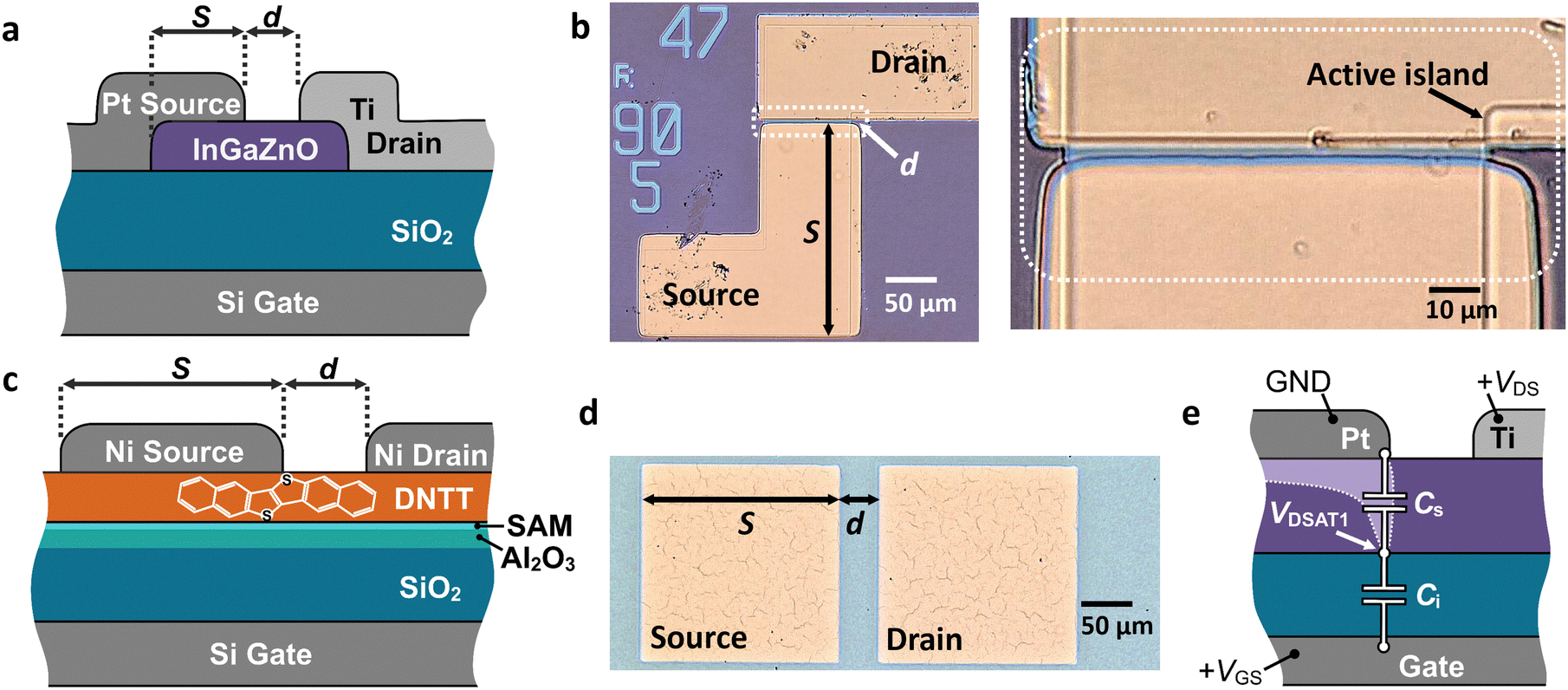 | ||
| Fig. 1 Schematic cross-sections (a), (c) and optical micrographs (b), (d) of staggered-electrode thin-film source gated transistors (SGTs) made with IGZO (a), (b) and DNTT (c), (d) via vacuum processing. Indicated are the source-gate overlap (S) and source–drain gap (d) along with the chemical structure of DNTT in the inset of (c). Due to the injection principles of SGTs, the source-gate overlap, S, of the active layer is a design parameter and is distinguished from source length. (e) Schematic representation of the source pinch-off condition showing the depletion envelope (dotted line) and the capacitive voltage divider pinning the voltage at the semiconductor–insulator interface to VDSAT1, as a sub-unity ratio of gate overdrive voltage. | ||
The top electrode metals are deliberately chosen to produce a weakly rectifying contact, to achieve source-gated transistor (SGT) operation.27,29 In the case of the DNTT SGT, both the source and the drain are made using nickel. The rectifying drain contact usually plays very little role in the region of operation considered, as it is forward-biased and significantly more conductive than the semiconductor channel and the reverse-biased source contact. The IGZO SGT has a rectifying platinum source and an Ohmic titanium drain contact.
To briefly review the distinct operation of source-gated transistors (Table 1), the rectifying source contact induces a depletion region within the semiconductor. When a relatively small drain–source voltage is applied, this depletion condition extends across the entire width of the semiconductor in the region of the source edge closest to the drain.27Fig. 1(e) describes schematically the behavior of an n-channel SGT. A positive gate-source voltage creates an accumulation layer, not only between the source and the drain (the geometrical separation d in Fig. 1 is equivalent in the first order to a conventional TFT's geometrical channel), but also underneath the source contact, where the gate and the source overlap over distance S (Fig. 1).28 This conductive layer is pinched off at the source edge by the application of a small drain–source voltage, resulting in the saturation of the output characteristics at a drain–source voltage VDS proportional to the overdrive voltage VGS − Vth, where Vth is the notional threshold voltage of the device, but also to the ratio of the potential divider formed by the specific capacitances of the depleted semiconductor and the gate insulator.27,28,30 It follows that, for a semiconductor with a large capacitance and a gate insulator of relatively low capacitance, the saturation voltage in SGTs can be substantially lower than in TFTs, as is its change with the applied gate-source voltage.30 Moreover, since the source area is responsible for restricting the current through the transistor,28 any variations of the geometrical or electrical properties within the source–drain gap (i.e., the channel) of the device will be well tolerated.25 With adequate design, the SGT can produce extremely flat output characteristics even in challenging material conditions.23,31 Together, these properties recommend source-gated transistors for a wide range of analog and digital functions.23
| Performance characteristic | TFT | SGT |
|---|---|---|
| V DSAT | High | Low |
| dVDSAT/dVGS | 1 | ≪1 |
| Drain current | High | Low |
| Power consumption | High | Low |
| Output impedance in saturation | Low | High |
| Intrinsic gain | Low | High |
| Off-current | Moderate | Low |
| Transconductance | High (quadratic) | Low (Linear/exponential) |
| Contact resistance | Low | High |
| Immunity to short channel effects | Poor | Excellent |
| Current stability in disordered semiconductors | Poor | Good |
| Temperature dependence | Low | High or low (design dependent) |
| Maximum operating frequency | Good | Moderate/poor |
DC output and transfer curves for DNTT and IGZO transistors are shown in Fig. 2. Both transistors show an on–off ratio of 107, with off-state drain currents below the noise floor of the measurement equipment (about 10−12 A). Importantly, the on-state drain current is comparable, on the order of 10 μA when operating in saturation at |VGS| = 20 V. Considering the similar channel width of the IGZO (W = 90 μm) and DNTT (W = 200 μm) SGTs, this feature is encouraging for sensible implementation of digital logic functions. The DNTT transistor is normally off, with a small negative onset voltage. In the case of the IGZO SGT, the onset voltage is positive and comparatively large. As a result, we expect that complementary inverter characteristics will exhibit a shift in the switching voltage.
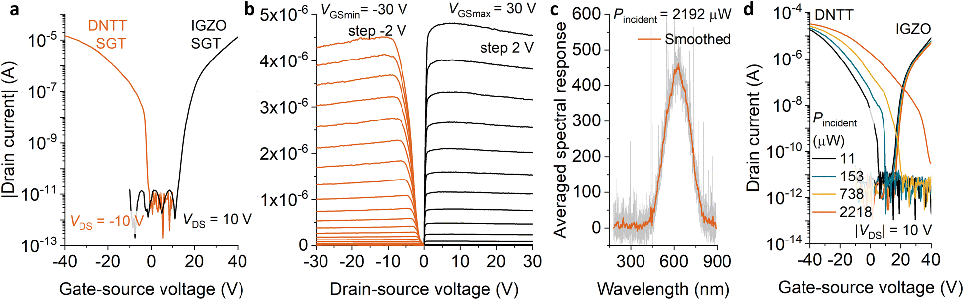 | ||
| Fig. 2 (a) Transfer and (b) output characteristics for the IGZO and DNTT SGTs having channel widths WDNTT = 200 μm and WIGZO = 90 μm. Both transistors operate in enhancement mode, have large on–off current ratio and similar on-state drain currents; (c) measured spectral response of the light source used for photostimulation; (d) transfer characteristics for the IGZO and DNTT SGTs under illumination using the light source in (c) at different intensities. | ||
The SGTs output characteristics (Fig. 2(b)) show early saturation in either type of device, with calculated saturation coefficient γDNTT = 0.26 and γIGZO = 0.21 comparing favorably to the extracted dVDSAT/dVGS values of 0.3 and 0.2, respectively.30 At high absolute gate-source voltage, both transistors exhibit negative differential resistance in the output curves. This has been observed in several SGT implementations26,30,32 and will be investigated separately. Nevertheless, flat output characteristics are obtained across a large range of operating conditions. Overall, these properties are close to ideal, and well suited to complementary digital logic realization.
Fig. 2 shows the effect of incident light (Fig. 2(c)) on the transfer curves (Fig. 2(d)). While a full treatment is beyond the scope of this study, the DNTT SGTs show a strong response in the subthreshold region,33 whereas this effect is far less pronounced in the IGZO transistors, owing to the wavelength considered and potentially to the shielding effect of the staggered electrode configuration. The low off-state current is maintained in both cases, as is the relatively low photosensitivity of the on-current at high absolute gate-source voltages. This dissimilar behavior is interesting to note in the context of future sensor development.
Inverter-circuit characterization
A complementary inverter circuit was realized with the two types of SGTs by making the connections via the probe station and source-measure unit, as previously reported.34 Since this method introduces extremely large parasitic capacitances in relation to the drive capability of the realized transistors, dynamic measurements would not have been representative and thus have been omitted. The parasitic resistances, however, are unlikely to play a significant role. The total resistance from source-measure unit to probe pad ranges from 0.2 to 2.1 Ω per channel, creating at most microvolts of series voltage drop, which does not represent a measurable contribution to either transistor output characteristics or the static performance of the circuit.The DC characteristics of the complementary inverters are presented in Fig. 3.
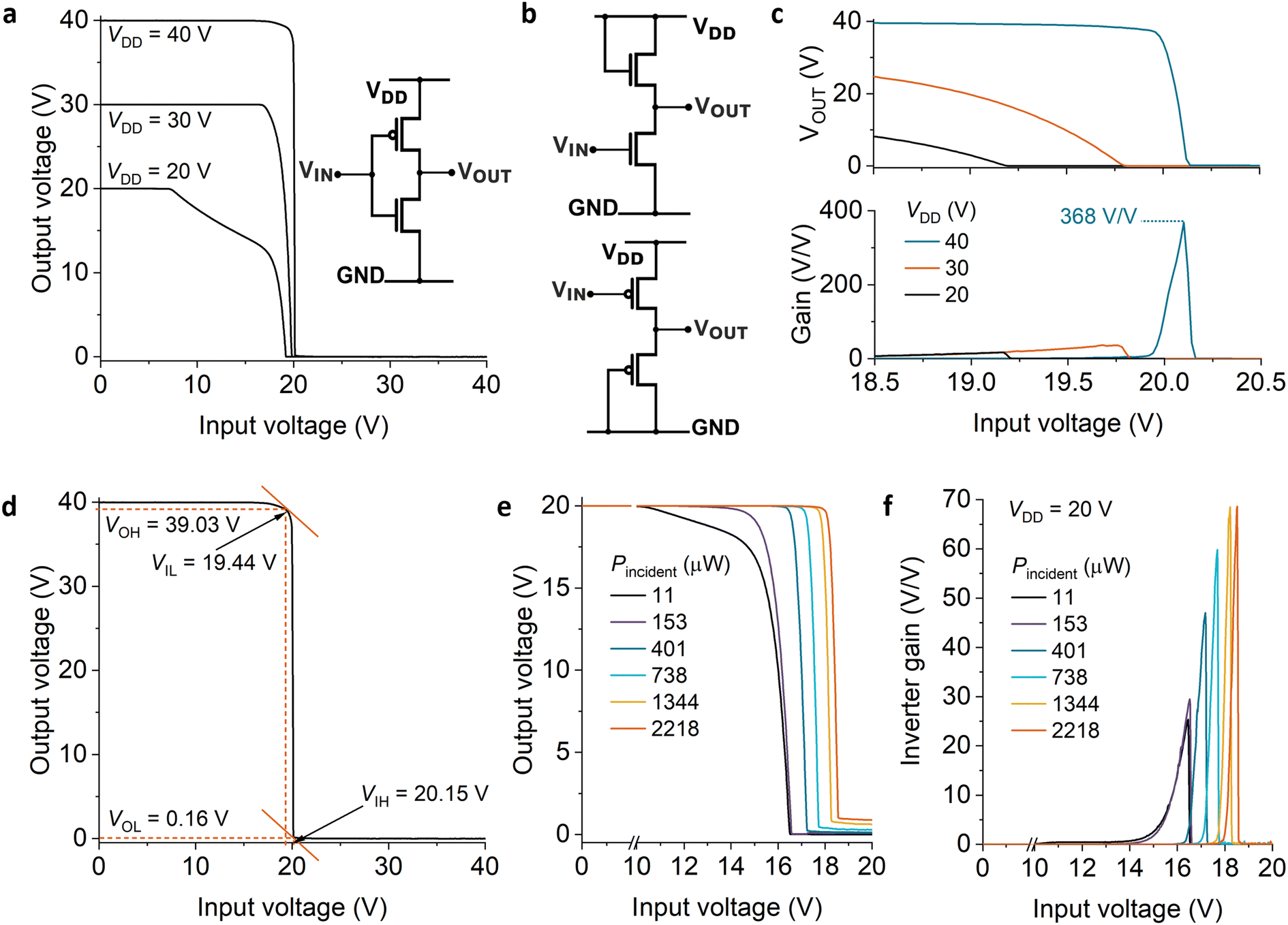 | ||
| Fig. 3 Low-frequency electrical characteristics of complementary inverters made with IGZO and DNTT source-gated transistors. (a) Inverter transfer curves at several power supply voltages, VDD, with circuit diagram inset; (b) circuit diagrams for n-channel (top) and p-channel (bottom) diode-load unipolar inverters; (c) detail of the region of interest around the switching voltage for the curves in (a); (d) voltage gain of the inverter circuit in (a) shown for the region of interest around the switching voltage with noise margin calculation for the inverter operating at VDD = 40 V; (e) inverter transfer characteristic under different illumination intensities; (f) inverter gain under different illumination intensities. | ||
Fig. 3(a) shows the transfer curve of the complementary inverter (schematic shown in the inset), measured at different supply voltages. As expected, the transitions are sharp and the switching voltage tends to the center of the supply voltage (VDD) range, as the current capability of the two devices matches closely at higher absolute drive voltage.
If implementation is practical, complementary realization of inverters is preferred to unipolar15 (e.g. diode-load circuits as illustrated in Fig. 3(b)), due to the fact that power dissipation is practically negligible in both logic states, with one of the transistors connected in series being turned off in this configuration. Fig. 3(c) shows a magnified view of the input voltage region of interest. In this same range of voltages, Fig. 3(d) shows the voltage gain, which peaks at 368 V V−1 at VDD = 40 V, a value in excess of any reasonable requirement and similar to that of complementary inverters based on organic TFTs.35 This is encouraging performance, considering that the constituent transistors did not include any lateral field-relief structures.23,30,34,36–38 The switching current exhibited for the small input voltage interval in which both transistors are conducting reaches a maximum of 130.5 nA for VDD = 40 V, for transistors with a channel width on the order of 100 μm. The switching power dissipation could be reduced by decreasing the channel width, but more so by increasing the effective energy barrier at the source contact. The decrease in drive current and transconductance will naturally result in a lower cut-off frequency. Depending on the application, this may be a suitable trade-off. For example, bio-signal recording or environmental monitoring applications require a modest bandwidth,39 and the power saving would be preferred.
For the case when the inverter trip point approaches VDD/2, the noise margin performance is also excellent, with values in excess of 18.8 V (94% of the theoretical maximum) for either logic values at VDD = 40 V (Fig. 3(f)).
The effects of photostimulation are shown in Fig. 3(g) and (h).
For digital applications, the shift in the tripping voltage of a complementary inverter could be used to sense incident light above a certain intensity by means of a change of logic state at a given bias point. More generally, the change in inverter gain could also be used in an analog implementation using feedback to translate changes in light intensity to voltage, current, or frequency changes.
The current demonstration is a first step toward proving the merits of this approach. Naturally, the integration of the organic and inorganic transistor poses its own challenges, and deserves due care and consideration, not least because of the different chemical and mechanical resilience of the two active materials. It should be, however, simply a matter of judicious process design, as reports exist of successfully co-patterning such active layers, including vacuum and solution techniques.40–43
Numerical simulation of source-gated transistors and inverters
A qualitative, first order simulation of the two types of transistors has been performed with Silvaco ATLAS. While our models can reproduce measured devices with great fidelity,44 here, the focus was on showing the net benefit of utilizing the complementary configuration over the diode-load topology for the inverter, realized with thin-film source-gated transistors.Output characteristics (Fig. 4(a) and (b)) show typical early saturation and flat output characteristics. From our observations, the negative differential resistance observed in fabricated devices (Fig. 2(b)) is bias-time dependent and is unable to be captured by the conventional d.c. “solve” statements in ATLAS. In future, we will be investigating these effects, along with their influence on the static and dynamic performance of logic gates in more detail.
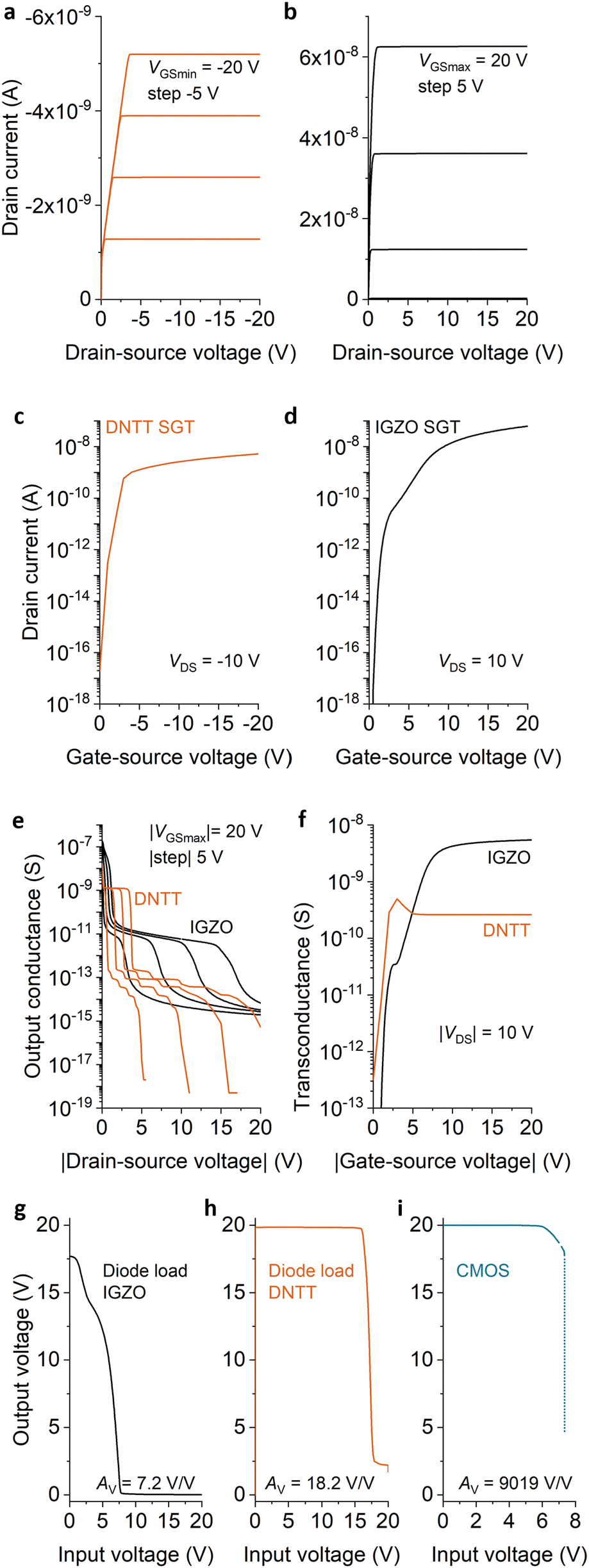 | ||
| Fig. 4 Simulated output (a), (b) and transfer (c), (d) characteristics for DNTT and IGZO source-gated transistors; (e) comparison of output conductance change with absolute drain–source voltage; (f) transconductance evolution with absolute gate-source voltage; inverter transfer characteristics and maximum gain for: (g) diode-load (IGZO), (h) diode-load (DNTT) and (i) complementary (IGZO-DNTT) inverter implementations. | ||
Transfer characteristics (Fig. 4(c) and (d)) show enhancement-mode operation, suitable for logic gate realization in either diode-load or complementary topology.
Fig. 4(e) and (f) show the evolution of essential ingredients for the intrinsic-gain performance of each transistor, namely output conductance (gd) and transconductance (gm). Since Av = gm/gd, ideally, gm should be large and gd small. Owing to the pinch-off process of the source-gated transistor configuration, saturated output curves can be very flat indeed, with extremely low values of gd.
It is interesting to note in Fig. 4(e) that both transistors show two plateaus in their gd values, corresponding to applied drain voltages between the source pinch-off voltage (VDSAT1) and the drain pinch-off voltage (VDSAT2) and above VDSAT2, respectively, as noted and analyzed previously,23,30,36,45 although this behavior cannot be inferred simply by inspecting the output characteristics, as the change in slope is practically negligible in both ranges.45
Transconductance (Fig. 4(f)) is comparatively low in both transistors, expected due to the constraint imposed on the drain current by the limiting process arising at the source contact. Even so, the intrinsic gain in these devices is 103–104 at low VDS and over 105 at high VDS. Thus, we expect that circuit configurations which make full use of the transistor's gain performance (complementary and, not applicable here, zero-VGS) would exhibit sharp transitions between logic states.
The diode-load inverter (Fig. 3(b)) is not able to achieve high gain, because the load device is always in a relatively low impedance state.34 Thus, as Fig. 4(g) and (h) show, the circuits are functional but have modest low-frequency switching performance. Conversely, the complementary inverter (Fig. 4(i)) exhibits a very sharp state transition, which makes it difficult for the numerical simulator to attain convergence. From the computed data, it is clear that the gain of this circuit is much superior to the diode-load configuration, making a strong case for complementary logic implementations. This holds true even if in this comparison no effort was made to position the trip point of the inverter in the middle of the supply voltage range, by geometrically matching the current drive of the n-channel and p-channel transistors, as, qualitatively, the result would have been similar, but at great time expense due to difficult numerical convergence.
Experimental
DNTT TFTs fabrication
Bottom-gate organic source-gated transistors (OSGTs) were fabricated on heavily p-type doped silicon substrates to take advantage of the Si as a gate electrode. The gate insulator stack comprised as follows: 100 nm thermally grown SiO2; 8 nm Al2O3, deposited by atomic layer deposition (ALD) at 250 °C; and a n-tetradecylphosphonic acid (C14H29PO(OH)2; PCI Synthesis, Newburyport, MA, USA)46 self-assembled monolayer (SAM), deposited via immersing the substrate into a 2-propanol solution with phosphonic acid. A 25-nm-thick active layer of dinaphtho[2,3-b:2′,3′-f]thieno[3,2-b]thiophene (DNTT, Sigma Aldrich)20 was vacuum deposited at a rate of 0.3 Å s−1 by thermal sublimation with the substrate temperature maintained at 60 °C. Source and drain contact electrodes were defined by thermally evaporating Ni through a shadow mask at a rate of 0.3 Å s−1. The mask features comprised contacts with channel width W = 200 μm and various source–drain separation d (also referred to as channel length L in conventional TFTs). The source-gate overlap is S = 200 μm by design, however this is shortened, due to the nature of probing. Probes are placed at the far end of the pad where S > 100 μm in order to measure the device where S would be injecting charge beyond SSAT. Single devices were isolated via scoring of the DNTT around the contacts to reduce the gate leakage current. The global bottom gate was contacted using a diamond scribe to expose the doped Si beneath the gate insulator stack.IGZO TFTs fabrication
Bottom gate a-IGZO SGTs were fabricated on Si/SiO2 wafer with heavily doped p-type doped Si with 85 nm thermally oxidized SiO2. The a-IGZO channel (In2O3![[thin space (1/6-em)]](https://www.rsc.org/images/entities/char_2009.gif) :Ga2O3:ZnO = 1:1:1) was deposited by radio frequency (RF) magnetron sputtering with power of 100 W at room temperature under an O2/(Ar + O2) ratio of 4.5% atmosphere and with a deposition pressure of 0.6 Pa (base pressure around 10−5 Pa). Next, the active layer was patterned by photolithography and wet etched with 0.02 M HCl. The source–drain separation and width of the SGT are 5 and 90 μm, respectively, with source-gate overlap S = 210 μm, which again ensures operation in the SSAT regime. The source and drain contacts were deposited separately. The 80 nm Pt source was deposited before the 80/20 nm, stack of Ti/Pt drain contact. The Ti/Pt contacts were deposited by RF sputtering with a power of 100 W at 10 and 5 sccm Ar, respectively. Finally, the samples were furnace annealed at 300 °C under N2:O2 = 4:1 atmospheric conditions for 2 hours. The Si bottom gate was again exposed by using a diamond scribe.
:Ga2O3:ZnO = 1:1:1) was deposited by radio frequency (RF) magnetron sputtering with power of 100 W at room temperature under an O2/(Ar + O2) ratio of 4.5% atmosphere and with a deposition pressure of 0.6 Pa (base pressure around 10−5 Pa). Next, the active layer was patterned by photolithography and wet etched with 0.02 M HCl. The source–drain separation and width of the SGT are 5 and 90 μm, respectively, with source-gate overlap S = 210 μm, which again ensures operation in the SSAT regime. The source and drain contacts were deposited separately. The 80 nm Pt source was deposited before the 80/20 nm, stack of Ti/Pt drain contact. The Ti/Pt contacts were deposited by RF sputtering with a power of 100 W at 10 and 5 sccm Ar, respectively. Finally, the samples were furnace annealed at 300 °C under N2:O2 = 4:1 atmospheric conditions for 2 hours. The Si bottom gate was again exposed by using a diamond scribe.
Device and circuit measurement
Devices and circuits were electrically characterized in dark and light conditions using a Wentworth probe station connected to a Keysight B2902A source/measure unit (SMU). Results from individual devices were compared, and devices with similar magnitude of drain current were selected for complementary circuit implementation. The circuits were manually connected using a six-probe setup and BNC cables. For the transfer and output characteristics, as per Fig. 2(a), (b), (d), and circuit results in Fig. 3(f) and (g), an OSGT with d = 40 μm was used. An OSGT with d = 20 μm was used for the remainder.Photostimulation setup
A Schott KL1500 LCD fiber optic cold light illuminator was used to expose devices and circuits to various light intensity at a distance of approximately 5 cm from the samples/circuits. The colour temperature of the light was set to 2650 K and the aperture was varied to increase the exposure, doubling with each increase in setting. The incident light was characterized using an Ocean Optics USB4000 spectrometer and a Gentec XLP12 spectral power meter. The thermal head has a 1.13 cm2 capture area, hence all incident light power corresponds to μW per 1.13 cm2. The lowest incident power Pincident was 11.05 μW, corresponding to the dark condition. External sources of light from other equipment are low and do not significantly affect device behaviour for the purposes of the study.Device simulation
Transistors were simulated in two dimensions using Silvaco ATLAS version 5.28.1.R.IGZO transistor geometry
The IGZO transistor was closely replicated to the measured device in a bottom-gate top-contact structure with highly doped p-type Si common gate and 85 nm thermally grown SiO2 gate insulator. The a-IGZO active layer was defined with source drain-separation and width of d = 5 μm and W = 90 μm, respectively. The Pt source was implemented by defining the contact work function to create a Schottky contact. Similarly, the Ti drain was defined with an Ohmic contact with a thickness of 80 nm. The source-gate overlap was S = 210 μm.IGZO transistor parameters
The reference structure was fabricated and replicated in the simulation with the density-of-states (DoS) of the simulated IGZO TFT having been modified to match the transfer and output curves of the device. Thus, by tailoring DoS, a good approximation can be made to the measured structure. For simulation of the IGZO active layer, the following DoS parameters were used: the effective density of states in the conduction and valence bands were NC = NV = 5.0 × 1018 cm−3; density of tail states at conduction band NTA = 3.0 × 1018 cm−3 eV−1; density of tail states at the valence band NTD = 3.0 × 1020 cm−3 eV−1; density of Gauss acceptor-like states NGA = 1.0 × 1016 cm−3 eV−1; density of Gauss donor-like states NGD = 1.0 × 1017 cm−3 eV−1; the relative permittivity of the gate insulator and semiconductor were εi = 3.9 and εs = 10, respectively; the electron affinity of semiconductor was 4.16 eV; the band gap and electron mobility were Eg = 3.1 eV and μn = 13 cm2 V−1 s−1, respectively; the work function of platinum and titanium were WF = 4.6 and 4.13 eV, respectively.DNTT transistor geometry
DNTT SGTs were simulated using previously verified material parameters as per Chen et al.44 The device geometry included 25 nm semiconductor layer thickness; 110 nm SiO2 gate insulator; 100 nm electrode thicknesses, with metals defined by using a work function. The source-gate overlap was set to S = 150 μm and source drain separation d = 8 μm.DNTT transistor parameters
DNTT material parameters were as follows: Eg = 2.9 eV; affinity of 2.9 eV; NC = NV = 3 × 1019 cm−3; metal work function WF = 4.88 eV, including barrier lowering parameter α = 2.7 nm with surface recombination enabled for the Schottky source contact; μp was set to 550 cm2 V−1 s−1. When taking into account the default organics default models,47 these parameters produce source-gated transistors operating with an apparent effective hole mobility in the order of several tenths of 1 cm2 V−1 s−1, which is in good agreement with fabricated devices.44Circuit simulation
Circuit simulations were performed using the Mixed-Mode capability of Silvaco ATLAS.47 The transistors were instantiated as ATLAS circuit elements, while the supply and input voltage sources were defined as SPICE components. To aid convergence, transient simulations with slow (100 ms) ramps of the input voltage have been implemented for the diode-load circuits. In the case of the complementary circuit, oscillations in the off state of the IGZO transistor made numerical convergence difficult. Hence, we adopted a piecewise dc simulation, first ramping the supply voltage to 20 V, then partitioning the input voltage range into regions with decreasing voltage steps (100 mV, 200 μV, 10 μV, 2 nV) to achieve a balance between compute time and fidelity. Even in these circumstances, the simulator was unable to converge fully, enabling us to state that the gain is in excess of 9000.Conclusions
We have reported the first complementary implementation of a thin-film source-gated transistor (SGT) based inverter using IGZO and DNTT n-channel and p-channel semiconductors, respectively. Given the flat output characteristics and early saturation of SGTs, attainable in the technologies used even in the absence of lateral field-relief structures, the complementary inverter shows excellent gain and noise margin.It is useful to remark that Ni and Pt both have relatively high work function. Through process optimization, it is conceivable that the same source contact metal may be used for both n- and p-channel transistors, potentially via specific surface treatment.
Moreover, we show that the trip point of such inverters can be tuned optically, with interesting applications in compact detectors and sensors.
This proof-of-concept demonstration provides encouraging initial results for further integration and circuit-level optimizations. Numerical simulation using Silvaco ATLAS show that, with adequate design, SGT-based inverters fabricated monolithically could reach gain levels in excess of 9000. Given their superior static performance, relative ease of fabrication and energy efficiency, such complementary inverters may find important uses in circuits for low and moderate speed digital processing of biological, user interaction, or health sensor data.
Author contributions
PS, UZ, EB, RAS led different parts of the investigation, performed the experiments and measurements. All authors were involved in setting out the methodology, conceptualisation and formal analysis. YU, JPB, HK and RAS supervised and validated the work, oversaw project administration and date curation. YU, HK and RAS were responsible for resource and funding acquisition. EB performed the visualisation, with assistance from all authors. RAS and EB wrote the original draft. All authors reviewed and edited the manuscript.Conflicts of interest
There are no conflicts to declare.Acknowledgements
Partial support for this project was provided by the Engineering and Physical Sciences Research Council, UK through grant no. EP/V002759/1. Travel between the Surrey and NAIST groups was made possible in part by the Royal Society of Great Britain International Exchange Programme Grant No. IEC\R3\183042, NAIST Grant in Aid, and partial support by JSPS Kakenhi No. 22K14291. RAS thanks Dr Ahmed Nejim for assistance with setting up the mixed-mode circuit simulations for improved numerical convergence.References
- E. Ozer, J. Kufel, J. Myers, J. Biggs, G. Brown, A. Rana, A. Sou, C. Ramsdale and S. White, Nat. Electron., 2020, 3, 419–425 CrossRef.
- M. Fattori, S. Cardarelli, J. Fijn, P. Harpe, M. Charbonneau, D. Locatelli, S. Lombard, C. Laugier, L. Tournon, S. Jacob, K. Romanjek, R. Coppard, H. Gold, M. Adler, M. Zirkl, J. Groten, A. Tschepp, B. Lamprecht, M. Postl, B. Stadlober, J. Socratous and E. Cantatore, Nat. Electron., 2022, 5, 289–299 CrossRef CAS.
- Y. Dai, H. Hu, M. Wang, J. Xu and S. Wang, Nat. Electron., 2021, 4, 17–29 CrossRef CAS.
- K. Myny, Nat. Electron., 2018, 1, 30–39 CrossRef CAS.
- L. Petti, N. Münzenrieder, C. Vogt, H. Faber, L. Büthe, G. Cantarella, F. Bottacchi, T. D. Anthopoulos and G. Tröster, Appl. Phys. Rev., 2016, 3, 1–53 Search PubMed.
- A. Tixier-Mita, S. Ihida, B. D. Ségard, G. A. Cathcart, T. Takahashi, H. Fujita and H. Toshiyoshi, Jpn. J. Appl. Phys., 2016, 55, 04EA08 CrossRef.
- A. F. Paterson and T. D. Anthopoulos, Nat. Commun., 2018, 9, 5264 CrossRef CAS PubMed.
- S. D. Brotherton, Introduction to Thin Film Transistors: Physics and Technology of TFTs, Springer International Publishing, Switzerland, 2013.
- J. F. Wager, Inf. Disp., 2020, 9–13 Search PubMed.
- M. Lorenz, M. S. Ramachandra Rao, T. Venkatesan, E. Fortunato, P. Barquinha, R. Branquinho, D. Salgueiro, R. Martins, E. Carlos, A. Liu, F. K. Shan, M. Grundmann, H. Boschker, J. Mukherjee, M. Priyadarshini, N. Dasgupta, D. J. Rogers, F. H. Teherani, E. V. Sandana, P. Bove, K. Rietwyk, A. Zaban, A. Veziridis, A. Weidenkaff, M. Muralidhar, M. Murakami, S. Abel, J. Fompeyrine, J. Zuniga-Perez, R. Ramesh, N. A. Spaldin, S. Ostanin, V. Borisov, I. Mertig, V. Lazenka, G. Srinivasan, W. Prellier, M. Uchida, M. Kawasaki, R. Pentcheva, P. Gegenwart, F. Miletto Granozio, J. Fontcuberta and N. Pryds, J. Phys. D: Appl. Phys., 2016, 49, 433001 CrossRef.
- H. Hosono, Nat. Electron., 2018, 1, 41928 Search PubMed.
- D. E. Gomersall, K. M. Niang, J. D. Parish, Z. Sun, A. L. Johnson, J. L. Macmanus-driscoll and A. J. Flewitt, J. Mater. Chem. C, 2023, 11, 5740–5749 RSC.
- P. R. Gray, P. J. Hurst, S. H. Lewis and R. G. Meyer, Analysis and design of analog integrated circuits, John Wiley & Sons, Inc., USA, 5th edn, 2009 Search PubMed.
- J. Zhang, J. Yang, Y. Li, J. Wilson, X. Ma, Q. Xin and A. Song, Materials, 2017, 10, 319 CrossRef PubMed.
- K. Nomura, J. Inf. Disp., 2021, 22, 211–229 CrossRef CAS.
- Y. Lee, J. Yoon, J. T. Jang, B. Choi, H. J. Kim, G. H. Park, D. M. Kim, D. H. Kim, M. H. Kang and S. J. Choi, AIP Adv., 2020, 10, 025131 CrossRef CAS.
- S. P. B. Sousa, T. Peixoto, R. M. Santos, A. Lopes, M. da, C. Paiva and A. T. Marques, J. Compos. Sci., 2020, 4, 106 CrossRef CAS.
- M. S. Oh, W. Choi, K. Lee, D. K. Hwang and S. Im, Appl. Phys. Lett., 2008, 93, 033510 CrossRef.
- I. Isakov, A. F. Paterson, O. Solomeshch, N. Tessler, Q. Zhang, J. Li, X. Zhang, Z. Fei, M. Heeney and T. D. Anthopoulos, Appl. Phys. Lett., 2016, 109, 263301 CrossRef.
- U. Kraft, K. Takimiya, M. J. Kang, R. Rödel, F. Letzkus, J. N. Burghartz, E. Weber and H. Klauk, Org. Electron., 2016, 35, 33–40 CrossRef CAS.
- J. M. Shannon and E. G. Gerstner, IEEE Electron Device Lett., 2003, 24, 405–407 CAS.
- G. Wang, X. Zhuang, W. Huang, J. Yu, H. Zhang, A. Facchetti and T. J. Marks, Adv. Sci., 2021, 2101473 CrossRef CAS PubMed.
- R. A. Sporea, M. J. Trainor, N. D. Young, J. M. Shannon and S. R. P. Silva, Sci. Rep., 2014, 4, 4295 CrossRef CAS PubMed.
- X. Xu, R. A. Sporea and X. Guo, in IEEE/OSA Journal of Display Technology, IEEE, 2014, vol. 10, pp. 928–933.
- R. A. Sporea, A. S. Alshammari, S. Georgakopoulos, J. Underwood, M. Shkunov and S. R. P. Silva, in European Solid-State Device Research Conference, 2013, pp. 280–283.
- E. Bestelink, H. Teng, U. Zschieschang, H. Klauk and R. A. Sporea, Adv. Electron. Mater., 2023, 9, 2201163 CrossRef CAS.
- J. M. Shannon, R. A. Sporea, S. Georgakopoulos, M. Shkunov and S. R. P. Silva, IEEE Trans. Electron Devices, 2013, 60, 2444–2449 Search PubMed.
- R. A. Sporea and S. R. P. Silva, in Proceedings of the International Semiconductor Conference, CAS, 2017, pp. 155–158.
- A. Valletta, L. Mariucci, M. Rapisarda and G. Fortunato, J. Appl. Phys., 2013, 114, 064501 CrossRef.
- E. Bestelink, U. Zschieschang, H. Klauk and R. A. Sporea, Adv. Electron. Mater., 2021, 8, 2101101 CrossRef.
- J. M. Shannon and F. Balon, IEEE Trans. Electron Devices, 2007, 54, 354–358 CAS.
- X. Zhuang, J. Kim, W. Huang, Y. Chen, G. Wang, J. Chen, Y. Yao, Z. Wang, F. Liu, J. Yu, Y. Cheng, Z. Yang, L. J. Lauhon, T. J. Marks and A. Facchetti, Proc. Natl. Acad. Sci. U. S. A., 2023, 120, e2216672120 CrossRef CAS PubMed.
- J. Milvich, T. Zaki, M. Aghamohammadi, R. Rödel, U. Kraft, H. Klauk and J. N. Burghartz, Org. Electron., 2015, 20, 63–68 CrossRef CAS.
- E. Bestelink, K. M. Niang, G. Bairaktaris, L. Maiolo, F. Maita, K. Ali, A. J. Flewitt, S. R. P. Silva and R. A. Sporea, IEEE Sens. J., 2020, 20, 14903–14913 CAS.
- S. C. Martens, U. Zschieschang, H. Wadepohl, H. Klauk and L. H. Gade, Chem. – Eur. J., 2012, 18, 3498–3509 CrossRef CAS PubMed.
- R. A. Sporea, M. J. Trainor, N. D. Young, J. M. Shannon and S. R. P. Silva, IEEE Trans. Electron Devices, 2012, 59, 2180–2186 CAS.
- Y. Hemmi, Y. Ikeda, R. A. Sporea, Y. Takeda, S. Tokito and H. Matsui, Nanomaterials, 2022, 12, 4441 CrossRef CAS PubMed.
- Y. Hemmi, Y. Ikeda, R. A. Sporea, S. Inoue, T. Hasegawa and H. Matsui, Adv. Electron. Mater., 2023, 9, 2201263 CrossRef CAS.
- T. Moy, L. Huang, W. Rieutort-Louis, C. Wu, P. Cuff, S. Wagner, J. C. Sturm and N. Verma, IEEE J. Solid-State Circuits, 2017, 52, 309–321 Search PubMed.
- M. Li, J. Wang, X. Cai, F. Liu, X. Li, L. Wang, L. Liao and C. Jiang, Adv. Electron. Mater., 2018, 4, 1800211 CrossRef.
- Z. Peng, F. Liu, H. Sun, Y. Wang, J. Wang and C. Jiang, IEEE J. Electron Devices Soc., 2021, 9, 933–938 CAS.
- H. Cheong, K. Kuribara, S. Ogura, N. Fukuda, M. Yoshida, H. Ushijima and S. Uemura, Jpn. J. Appl. Phys., 2016, 55, 04EL04 CrossRef.
- K. G. Cho, H. J. Kim, H. M. Yang, K. H. Seol, S. J. Lee and K. H. Lee, ACS Appl. Mater. Interfaces, 2018, 10, 40672–40680 CrossRef CAS PubMed.
- M. Chen, B. Peng, R. A. Sporea, V. Podzorov and P. K. L. Chan, Small Sci., 2022, 2100115 CrossRef CAS.
- R. A. Sporea, M. J. Trainor, N. D. Young, J. M. Shannon and S. R. P. Silva, IEEE Trans. Electron Devices, 2010, 57, 2434–2439 CAS.
- S. Bisoyi, R. Rödel, U. Zschieschang, M. J. Kang, K. Takimiya, H. Klauk and S. P. Tiwari, Semicond. Sci. Technol., 2016, 31, 025011 CrossRef.
- Atlas User's Manual: Device Simulation Software, Silvaco Inc., 2016 Search PubMed.
| This journal is © The Royal Society of Chemistry 2023 |