
 Open Access Article
 This Open Access Article is licensed under a Creative Commons Attribution-Non Commercial 3.0 Unported Licence
Particle size effect on the microstructure and the aging process of flash-sintered barium titanate from micro and nanopowders†
Samuel
López-Blanco
 *a,
Xavier
Vendrell
b,
Lourdes
Mestres
b,
Diego A.
Ochoa
a and
Jose E.
García
a
*a,
Xavier
Vendrell
b,
Lourdes
Mestres
b,
Diego A.
Ochoa
a and
Jose E.
García
a
aDepartment of Physics, Universitat Politècnica de Catalunya – BarcelonaTech, 08034 Barcelona, Spain. E-mail: samuel.lopez.blanco@upc.edu
bDepartment of Inorganic and Organic Chemistry, Universitat de Barcelona, 08028 Barcelona, Spain
First published on 8th August 2023
Abstract
Flash sintering is a novel sintering technique that allows high-density ceramics to be obtained at low temperatures and using short dwell times, thus providing an energy-efficient alternative to conventional sintering. The microstructure of flash-sintered samples can be fine-tuned by a proper control of electrical parameters such as current density, electric field, and current profile, yielding significant improvements of functional properties. The starting powder should also be carefully selected since better sintering results are reported for smaller green grain sizes. However, this work evidences time evolution of electrical properties of flash-sintered BaTiO3 ceramics from submicron powders. The results reveal that these transformations greatly depend on powder grain size and can be further adjusted with an adequate selection of electric power profiles. This work provides new insights into ongoing phenomena during field-assisted sintering, such as grain growth and defect formation dynamics. Although the results focus on BaTiO3, it offers a new pathway to tailor the microstructure of flash-sintered ceramics, which may be extended to other electronic materials.
1. Introduction
Ceramic manufacturing is still based on the traditional sintering technique, which is very energy inefficient because lengthy, high-temperature heat treatments are required. Nowadays, world events point out the need to reduce energy consumption and the environmental impact related to the industrial production of ceramic materials. In this regard, field-assisted flash sintering has arisen as a compelling energy-efficient technique since it has proven to significantly reduce sintering time and temperature via electric field application.1 Although a flash sintering experiment involves many parameters such as sintering atmosphere, powder size, electric field, electric current, and current profile, among others, an adequate control of them has been shown to dictate the sample properties crucially.2,3 Several phenomenological descriptions of the flash sintering underlying mechanisms have been proposed, yet a unanimous consensus has still not been reached.4–6Due to its novelty, flash sintering viability is yet to be studied for many systems, especially for functional materials.7,8 In particular, works related to flash sintering of ferroelectric compositions are scarce and typically focused on obtaining dense ceramics with suitable microstructure,9–13 tending to ignore the microstructure–properties relationship. BaTiO3 (BTO) is an extensively studied ferroelectric material widely regarded as a perovskite-structured model of polar oxide. Therefore, BTO is used as an archetype system for a wide variety of studies involving grain and scaling effects, and doping effects, among others.14 Binary and ternary BTO-based ferroelectric systems have also been developed, chemically designed to show enhanced properties for specific applications.15,16 Both undoped and doped BTO were recently proven to be achievable via flash sintering,9,10 and fine microstructure tuning has been proven to be obtained by a proper electric current control.17
In this work, two different-sized commercial powders of BTO are subject to flash sintering experiments, evidencing the influence of working conditions over the achieved microstructures and, consequently, functional properties. Moreover, we take a step further and report the presence of a time instability of properties as a consequence of flash sintering for smaller powder sizes, which appears to be linked to an abnormal grain size distribution. The aging of the properties also depends on the specific electric profile, hinting towards the influence of electric power over defect formation during flash sintering. This report clashes with the established idea that sintering from nanopowders achieves better densification at lower temperatures and was therefore thought to be the best powder option for flash sintering experiments.18
2. Experimental procedure
2.1 Sintering experiments
Commercial powders of BaTiO3, provided by Sigma Aldrich, are used for sintering experiments. Particle sizes with average grain size of ∼2 μm (Sigma Aldrich, 99.5%, ref. 338842, hereafter referred to as micropowder) and ∼100 nm (Sigma Aldrich, ≥99%, ref. 467634 hereafter referred to as nanopowder) are used. Dog bone pellets (Fig. S1a, ESI†) are obtained using a 270 MPa uniaxial load to form the initial green sample (GS). The GS is suspended in the center of the furnace using two platinum wires attached to its handles following a typical flash sintering experiment setup (Fig. S1b, ESI†). A homemade software controls the programmable DC power supply (Ametek XG 600-2.6), changing its operation mode automatically upon reaching the previously set current limit. Platinum paint (SPI Supplies, 04990-AB) mixed with platinum paint thinner (SPI Supplies, 04989-AB) is used in order to ensure electrical contact between the sample and the platinum wire electrodes. A uniform electric current flow along the sample is achieved using an adequate paint geometry mimicking a plane parallel capacitor (Fig. S1a, ESI†). A CCD camera records the samples’ luminescence and shrinkage.Both conventional flash sintering (CF) and controlled current flash sintering (CCF) experiments are carried out in order to study the influence of the electric current profile (Fig. S2, ESI†) on the microstructure.19 For a CF experiment, the sample is heated at a furnace rate of 10 °C min−1 from room temperature while a constant electric field is held until the current runaway takes place; at this time, the power source changes to constant current mode (Fig. S2a, ESI†). The sample is left to dwell for a fixed time, and then both furnace and power supply are turned off to let the sample cool naturally. For CCF experiments, the sample is also heated at a furnace rate of 10 °C min−1 but no electric power is applied until reaching the preset temperature of 950 °C, where the sample is held exclusively under current control. After reaching the maximum preset current, the sample is left to dwell and then cools naturally, like in a CF experiment. Current profiles are selected (i.e., conventional, ramp, step, quadratic and square root) so that the current limit is reached at the same time in all cases (Fig. S2b, ESI†). The sample’s resistivity during flash sintering is evaluated to study the intrinsic uncertainty of the results and their reproducibility due to the nature of the electrical contacts. All tested samples achieve similar resistivity values during the dwell stage; that is, when the same electrical conditions are applied (Fig. S3, ESI†) such that the flash sintering experiments are not critically affected by the electrical contacts.
In order to ensure reproducibility and minimize density inhomogeneities, sintered specimens are cut far from the vicinity of the electrical contacts in a rectangular cuboid shape (10 mm × 3 mm × 0.7 mm). The Archimedes method is used to measure density. Density gradients are known to appear due to the nature of the flash sintering technique, but they can be lessened by proper control of the flash event.2,3 Scanning electron microscopy (SEM) images show no visible presence of density gradients, as shown in a representative illustration in Fig. S4 (ESI†).
2.2 Microstructure and functional properties
The microstructure is evaluated using a field-emission scanning electron microscope (JEOL, JSM-7001F), for which samples are firstly polished and chemically etched for 1 min. The grain size distribution is determined from SEM images by processing an area of no less than 1000 grains. In order to electrically characterize the samples, electrical contacts are applied on the samples' parallel faces using gold coating sputtering. Permittivity values of unpoled samples are measured using an LCR meter (Agilent E4980A) from about 520 K to 20 K at frequencies ranging from 100 Hz to 1 MHz. Electric field–induced polarization (P–E) hysteresis loops are measured in a typical Sawyer–Tower configuration by applying a triangular electric field of amplitude of 2 kV mm−1 at a frequency of 1 Hz at room temperature. Impedance spectroscopy experiments are carried out using a frequency response analyzer (AMETEK Solartron Analytical). Impedance values are recorded using a frequency sweep ranging from 100 mHz to 1 MHz at different temperatures. Samples are heated in a furnace from room temperature using a ramp of 5 °C min−1 until the desired temperature is reached; at this point, the sample is left for 10 min to allow thermal stabilization. Impedance spectroscopy data is analyzed following the work of Irvine et al.203 Results and discussion
3.1 Conventional flash sintering
Powder selection is a crucial factor for optimizing the flash sintering process. For instance, smaller powder sizes are known to reduce the onset temperature for a given electric field (or, equivalently, the onset electric field for a given temperature) and improve the final density of the sintered samples.18 Here, the relations between electric field, onset temperature, and density are studied for flash sintering of BTO from both micro and nano-sized powders, and the results are gathered in Fig. 1. Electric current density limit and dwell time are set at 15 mA mm−2 and 10 min, respectively. As previously mentioned, the smaller powder requires a lower temperature to sinter when the same conditions as for the micrometric powder are applied, but the results show that the parameter region in which dense samples are obtained is narrower for sintering from the nanopowder. The sample’s density decreases directly with the electric field for both cases in accordance with the literature.9 In a previous work, we found that a homogeneous microstructure is obtained for flash-sintered BTO from micropowder and that the main electrical parameter affecting grain growth is the electric current, while the electric field does not seem to have a discernible effect.17 This result is replicated in this experiment and recorded in Fig. 1f–h. Similar results are obtained for flash-sintered BTO from nanopowder, as shown in Fig. 1c–e, but the sintered microstructure appears to be very heterogeneous.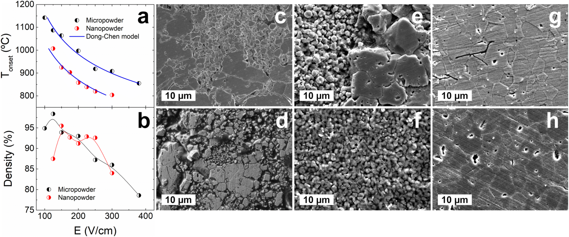 | ||
| Fig. 1 (a) Sintering temperature (Tonset) and (b) relative density of samples obtained in conventional flash experiments carried out using different electric field values (E). Current density and dwell time have been maintained at 15 mA mm−2 and 10 min, respectively. The Dong–Chen model21 is used to validate the dependence of Tonset with E, showing a reasonable fit to the experimental data. (c)–(e) Representative micrographs of samples obtained in conventional flash sintering experiments using nanopowder under different electric conditions: (c) 150 V cm−1 and 10 mA mm−2, (d) 200 V cm−1 and 10 mA mm−2, (e) 150 V cm−1 and 15 mA mm−2. (f)–(h) Representative micrographs of samples obtained in conventional flash sintering experiments using micropowder under different electric conditions: (f) 150 V cm−1 and 10 mA mm−2, (g) 200 V cm−1 and 15 mA mm−2, (h) 150 V cm−1 and 15 mA mm−2. Dwell time has been maintained at 10 min for all cases. Bigger grains are obtained with increasing electric current. A heterogeneous microstructure is displayed for samples obtained from nanopowders. | ||
Fine powder is known to enhance sintering due to improved reactivity related to a higher free surface energy,22 but it seems to introduce unexpected phenomena when interacting with the electric field and the out-of-equilibrium nature of the flash sintering technique. In order to evaluate this possibility, the real-time densification of different samples is studied using video data. Results are shown in Fig. S5 (ESI†), where samples display different behaviors depending on the powder size. Samples obtained from micropowder begin to shrink near the flash event, with most of the contraction occurring during dwelling. On the other hand, samples obtained from the nanopowders experience the majority of their shortening steadily since the incubation stage, so dwell has minimal effect regarding their final length. Moreover, depending on the electrical conditions, different trends appear for the shrinkage of the samples obtained from nanopowders, showing a strong influence of the electric sintering parameters on the shrinkage mechanism. It can be speculated that the samples densification mechanism strongly depends on the starting powder size when undergoing flash sintering, which is further supported by the fact that nanometric and micrometric powder mixtures were flash-sintered with disappointing results (a higher furnace temperature was needed for the flash event to take place and lower densities were achieved, as recorded in Fig. S6, ESI†). It should be noted that shrinkage is not a good measure of density, as seen in Fig. S7 (ESI†), where no correlation is found between both magnitudes. Samples tend to shrink more along the electric field axis in a non-isotropic manner, so this measurement should not be taken as direct information regarding the density of the samples. Shrinkage measurements are, therefore, only used to qualitatively analyze the densification behavior during flash sintering.
As previously mentioned, samples obtained from nanopowder have a very inhomogeneous microstructure. Fig. S8b–d (ESI†) shows the presence of both bimodality and abnormal grain growth for these samples at different sintering conditions. It is worth noting that samples obtained from nanopowder have a few grains that grow abnormally but contribute heavily towards the total sample volume. At the same time, their conventionally-sintered counterpart (Fig. S8a, ESI†) follows the same behavior as the samples obtained from micropowder. However, this abnormal growth depends on the electric sintering conditions (Fig. S8b–d, ESI†), where higher current densities create a bimodal microstructure and higher electric fields tend to prevent the formation of huge abnormal grains. On the other hand, samples obtained from micropowder (Fig. S8e–h, ESI†) tend to follow a lognormal distribution of their grain sizes, achieving around 50% of their cumulative volume near the distribution peak.
Powder selection seems to affect not only the densification profile but also the resulting microstructure, which could have unforeseen consequences regarding the sample properties. Two interesting features are noticed in the samples sintered from nanopowders: (i) samples become macroscopically conductive a couple of weeks after sintering, causing a sharp evolution in their functional properties; and (ii) the density drops after a year, while their micropowder counterparts stay stable (Fig. S9, ESI†). These samples also exhibit a slight increase in their thickness after a long period of time, which could explain the density drop. This swelling is yet to be fully understood, although we hypothesize it might be related to the stress relaxation associated with lattice mismatch and/or to a change in the lattice parameter due to reoxygenation of the flash-sintered reduced lattice.23,24
It is well-known that the dielectric response of BTO suffers a mild aging effect whose origin is still debated.19,25 However, the aging effect reported in this work is much faster than the one reported in the literature. Moreover, no discussion about the change in BTO density with time has been found, leading to the assumption that the time evolution of properties reported here for flash-sintered samples obtained from nanopowder differs from the conventionally reported aging process. Therefore, a flash-induced aging process seems to appear for samples obtained from nanopowders, which will henceforth be labeled as FINA (flash-induced nanopowder aging). Because flash sintering is known to be able to induce the formation of metastable phases8 that could explain the observed FINA, synchrotron XRD measurements are done in order to evaluate the presence of spurious phases. Diffraction patterns of flash-sintered samples obtained from both micro and nanopowders are compared in Fig. S10 (ESI†), where no apparent differences are observed. No spurious phases are detected. Lattice parameters are calculated using peak analysis for both samples, obtaining tetragonality values of 1.0089 and 1.0093 for samples obtained from nanopowder and micropowder, respectively. The difference in the tetragonality could be attributed to the stress induced during sintering or the lattice mismatch between the matrix and the abnormally big grains in the sample obtained from nanopowder.26
In order to probe the origin of the FINA, three new samples are prepared to study the evolution of their functional properties: (i) flash-sintered BTO from micropowder at 150 V cm−1, 15 mA mm−2, 10 min dwell time; (ii) conventionally-sintered BTO from nanopowder, following a typical sintering scheme (Fig. S11, ESI†); (iii) flash-sintered BTO from nanopowder at 150 V cm−1, 15 mA mm−2, 10 min dwell time. Results from impedance spectroscopy analysis are displayed in Fig. 2, showing that the main factor affecting the aging process is a combination of both the nanopowder and the flash sintering route. The flash-sintered sample from micropowder suffers a small decrease in grain boundary resistance (Fig. 2b), while bulk resistance (Fig. 2a) and capacitances (Fig. 2e and f) seem to undergo no significant change. For the case of conventional sintering from nanopowder, the specimen not only stays immutable with time (Fig. 2c and g) but also yields the highest values of impedance (i.e., it works as an ideal capacitor, obtaining capacitance and impedance values that exceed our device measuring range). However, when the nanopowder is used for flash sintering, the resulting sample exhibits both bulk and grain boundary resistivities that strongly reduce over time (around an order of magnitude decrease for 14 days, as shown in Fig. 2d). In addition, both bulk and grain boundary capacitances significantly increase as reported in Fig. 2h.
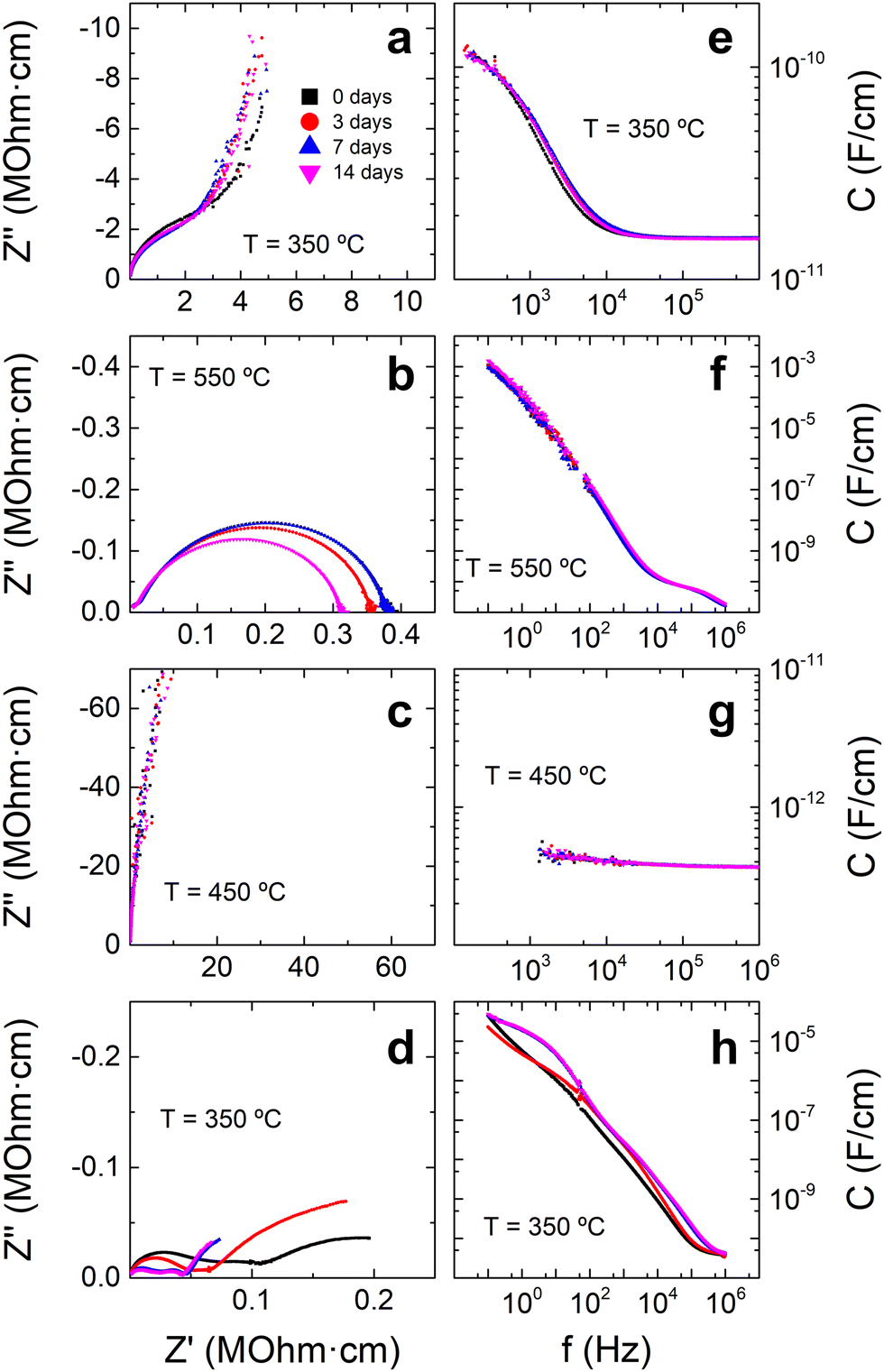 | ||
| Fig. 2 Time evolution of (a)–(d) Nyquist plots and (e)–(h) capacitance versus frequency response of samples sintered under different conditions: (a), (b), (e) and (f) flash-sintered from micropowder; (c) and (g) conventionally-sintered from nanopowder; (d) and (h) flash-sintered from nanopowder. Samples were flash-sintered at 150 V cm−1 and 15 mA mm−2 with a dwell time of 10 min. | ||
To better understand the time evolution of the electrical properties of the flash-sintered samples from nanopowder, temperature dependence of the conductivity is studied. A flash-sintered sample from micropowder is also examined for comparison. Fig. 3 shows that, initially, all samples have the same behavior at high temperatures (above 200 °C), suggesting roughly equal activation energy for conduction of 0.82 eV. This value is similar to the reported migration energy for oxygen vacancies in BTO, pointing towards the possible presence of these defects.27 However, the flash-sintered samples from nanopowder appear to have an electronic-like contribution to the conduction at low temperatures. This is characterized by the decrease of the conduction with temperature, but with a conductivity value several orders of magnitude below what would be expected for metallic conduction.28 This regime also depends on the sintering conditions, hinting that the microstructure (or defects structure) influences the non-ionic conduction. Furthermore, the conductivity of these samples undergoes a complex evolution for both low and high temperatures, while no changes are detected for the sample sintered from micropowder. A more detailed analysis is shown in Fig. S12 (ESI†), where it may be seen that the low-temperature regimen splits, which could indicate the presence of electrochemical reactions or a mixed conduction regime.29
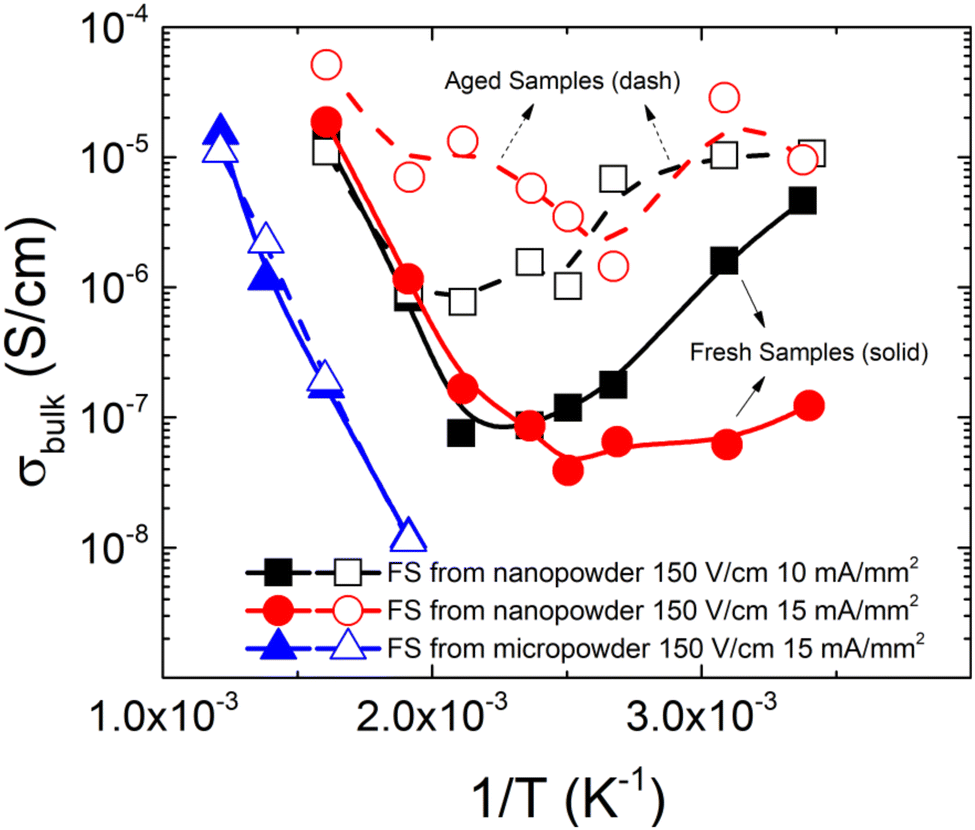 | ||
| Fig. 3 Time evolution of bulk conductivity for samples flash-sintered under different conditions. Filled points and solid lines correspond to measurements taken after sintering the sample, while hollow points and dashed lines correspond to data taken two weeks after sintering. The flash-sintered sample from micropowder stays stable, whereas flash-sintered samples from nanopowder evolve, showing an electronic-like contribution to conductivity at low temperatures that disappears after heating at around 200 °C. The samples obtained from micropowder have a low temperature resistivity value higher than the experimental detection limit. | ||
Although the microscopic origin of this phenomenon is still unknown, aging is found to be strongly related to the microstructure. Flash-sintered samples from nanopowder show a very heterogeneous microstructure alongside abnormal grain growth, while the samples that manifest no impactful aging (i.e., the conventionally-sintered nanopowder and the flash-sintered micropowder) have a well-defined and homogeneous microstructure, as shown in Fig. 4. This result allows us to speculate that this abnormal structure arises as a consequence of the flash sintering of highly reactive submicron-powders, which in turn could be responsible for the FINA process. Since the samples are stored at room temperature under atmospheric conditions, we hypothesize that defect dynamics may be the leading phenomenon governing the behavior of the samples. Moreover, an important difference can be made between the low-temperature and high-temperature regimes: the low-temperature electronic-like contribution to conductivity disappears after thermal treatment for an aged sample, while the high-temperature contribution retains the same behavior with a lower total conductivity value (Fig. S13, ESI†). The electronic-like contribution, however, reappears after around 2 days, indicating that the sample tends to become conductive with time, even after the heat treatment.
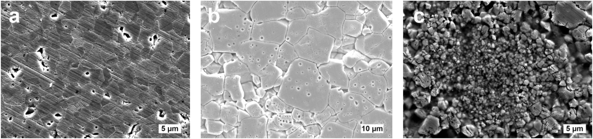 | ||
| Fig. 4 SEM micrographs of samples sintered under different conditions: (a) flash-sintered sample from micropowder at 150 V cm−1 and 15 mA mm−2; (b) conventionally-sintered sample from nanopowder; (c) flash-sintered sample from nanopowder at 150 V cm−1 and 15 mA mm−2. | ||
The impedance measurement protocol involves heating the samples until up to 500 °C such that the sample undergoes a heat treatment every time a set of measurements is done. As a result, the low-temperature conductivity regime modifies and, therefore, it may yield false information about its time evolution (we can only report how it changes between measurements). Therefore, to establish an adequate measuring protocol, only the high-temperature conductivity regime will be considered hereafter, excluding the electronic-like conduction regime.
To summarize, a thorough study on flash sintering conditions for nanometric and micrometric BTO powders has been done. Results show nanopowders require lower energy for the flash sintering event to occur, leading to better densification. However, an aging effect regarding density and functional properties becomes apparent for nanopowders, which has not previously been reported. This phenomenon appears to be related to the microstructure inhomogeneity induced by the flash sintering, and it seems to be a consequence of defect generation dynamics.
3.2 Controlled current flash sintering
Current density rate is known to be an electrical parameter that affects the microstructure during a flash sintering experiment. It has been demonstrated that applying a slow current ramp during the incubation stage helps achieve better densification and microstructure homogeneity, although there is no consensus on the microscopic origin of these enhancements.3,30–33 In a previous work,17 the influence of the current density profile during flash sintering over the microstructure and functional properties of BTO obtained from micropowder was widely discussed. It was reported that improved densification and enhanced functional properties were observed for initially low electric current slopes and current rates, which hints that defect dynamics play an important role during flash sintering.In this regard, if the FINA process is related to defect dynamics, the choice of different current profiles during flash sintering should lead to different defect structures and, therefore, different functional properties. For this purpose, a new set of samples are flash-sintered at 950 °C under current control using different current profiles (Fig. S2b, ESI†). Shrinkages for these flash sintering experiments are reported in Fig. S14 (ESI†), where different behaviors appear depending on the current profile, thereby evidencing the importance of the instantaneous electric current and electric field values during flash sintering. Microstructures of current-controlled flash sintering (CCFS) samples are reported in Fig. S15 (ESI†), showing a clear difference in both grain size and grain size distribution when different current profiles are employed (a detailed study of the grain size and volume distributions is reported in Fig. S16, ESI†).
Both conductivity and activation energy are recorded for all flash sintering profiles over a period of two weeks. Results are plotted in Fig. 5, where bulk and grain boundary contributions are separated from the total conduction. Firstly, it is interesting to note that different profiles show slightly different activation energy values, which can be attributed to differences in the defect microstructure. Secondly, two different behaviors are apparent when the time evolution of the samples is examined: square root, conventional and step profiles remain arguably constant regarding their total conductivity, while both ramp and quadratic profiles have a sharp decrease in their total activation energy and an increase in conductivity.
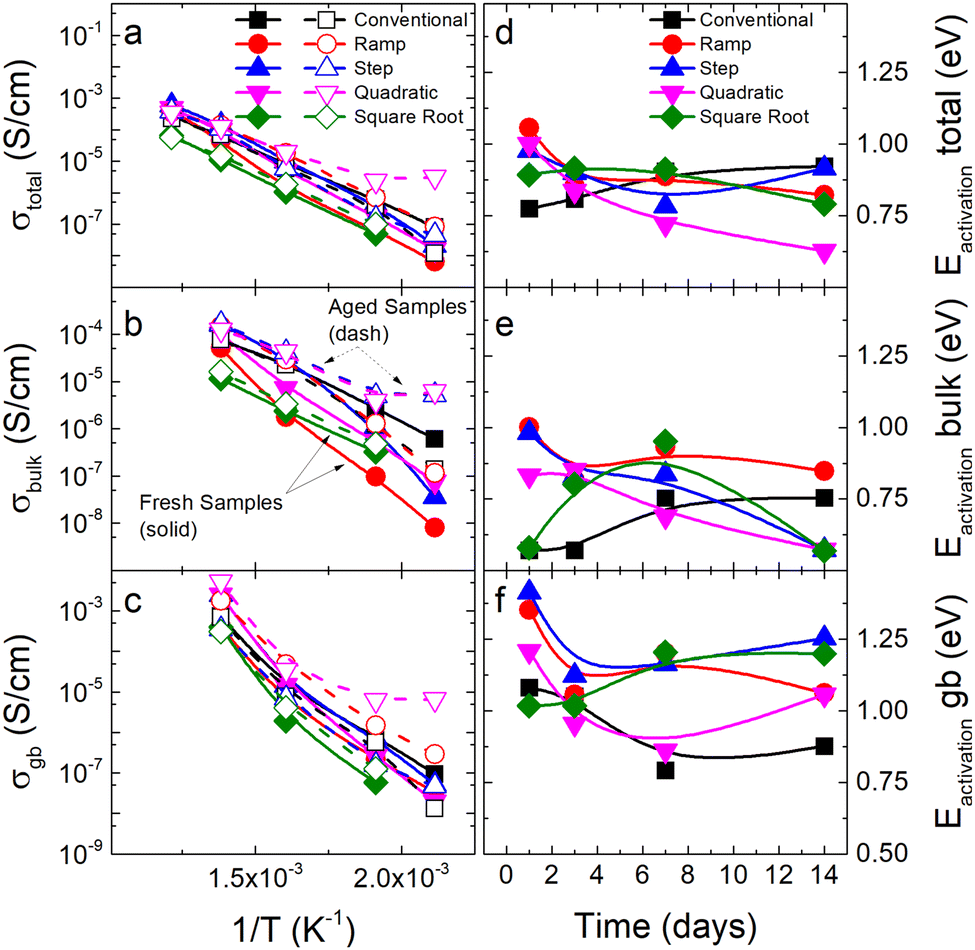 | ||
| Fig. 5 (a)–(c) Arrhenius plots of conductivity and (d)–(f) activation energy values for samples flash-sintered using different electric current profiles. Bulk contribution, grain boundary contribution, and total conductivity values are given for freshly sintered samples (solid points and lines) and are compared to the same samples but aged 14 days (hollow points and dashed lines). Conductivity changes with time, and its Arrhenius plots also change in slope, suggesting an evolution of conduction mechanisms. Different current profiles manifest different evolution in their activation energies. | ||
Grain boundary, bulk activation energies, and conductivities exhibit complex behaviors for all samples, suggesting the existence of several processes or electrochemical reactions during flash sintering. In particular, the sample obtained using the quadratic current profile shows the sharpest time evolution of properties and the most heterogeneous microstructure. Furthermore, the aged sample exhibits super-Arrhenius-like behavior for all conductivity contributions, even for temperatures above 200 °C. This phenomenon has already appeared in previous experiments (Fig. S12, ESI†), but for this case, there appears to be a shift in temperature with time. In fact, it can be shown (Fig. S17, ESI†) this sample exhibits more than the three typical contributions to conductivity (i.e., bulk, grain boundary, and interface contributions), thereby indicating the possible presence of a chemical reaction or mixed conduction for high temperatures that disappears with time.29 This process, however, is not exclusive to this sample: most of the CCFS samples exhibit this behavior when measured three days after sintering, suggesting a clear evolution of the sample properties is present even for the high-temperature Arrhenius regimen (Fig. S17, ESI†).
3.3 Origin of the FINA process
Functional ceramics are known to become slightly conductive after sintering due to the formation of oxygen vacancies during the process.34 Moreover, BTO is known to be an ionic conductor in the range of 300–500 °C,35 but it can become a mixed conductor due to oxygen nonstoichiometry.36 In this regard, samples sintered using nanopowder are more susceptible to the existence of these defects,22 which tend to disappear after heat treatment or long exposure to the ambient atmosphere. Here, this phenomenon appears to be evident, as shown in Fig. S18 (ESI†), where the evolution of hysteresis loops is recorded for conventionally-sintered samples from both BTO powders. Initially, the sample obtained from the nanopowder is more conductive than the micropowder counterpart, which can be explained in terms of a higher concentration of oxygen vacancies due to the higher reactivity of the nanopowder. After a year of air exposure, oxygen vacancies tend to disappear, and the samples become less conductive. In contrast, when the BTO nanopowder is flash-sintered, an opposite trend is evidenced (Fig. S9c, ESI†): the samples tend to become more conductive and exhibit electronic conduction for the first weeks after sintering. This is further supported by the shift of the paraelectric transition of a CF sample towards higher temperatures with time (Fig. S19, ESI†), which can be explained in terms of a higher concentration of oxygen vacancies37 or lattice stress relaxation.38,39The evolution of the impedance given in Fig. 2 and the corresponding activation energy shift towards lower values reported in both Fig. 3 and Fig. S12 (ESI†) can also be explained regarding oxygen vacancies generation. It has been reported that electron transport in BTO doped with oxygen vacancies becomes metallic above a critical electron concentration,40 which also explains the observed electronic-like conduction.41 The mixed conduction regime reported in Fig. S12 (ESI†) implies the presence of some electrochemical or stress-related phenomenon that favors the formation of vacancies, which in turn could explain the unusual impedance arcs reported in Fig. S17 (ESI†). For the case of CCFS samples, the same arguments can be made. EDS measurements (Fig. S20, ESI†) of the CCFS sample obtained using a quadratic current profile show a difference in the composition of the grains, shifting from 58.3% atomic oxygen in small grains to 54.9% in abnormally grown grains. It is known that during flash sintering, oxygen is consumed from the environment to annihilate the oxygen vacancies and corresponding defects, playing a major role in rapid densification.34 In the case of highly reactive nanopowders, the oxygen vacancies formation rate may be too high, and total annihilation might be impossible, leading to defects accumulation in the abnormally grown grains.34,42,43
In order to probe the oxygen vacancy formation hypothesis, a CCFS sample obtained using the quadratic profile is cut in two halves, and each one of them is kept in different conditions for three weeks: one in a furnace at 800 °C and the other in vacuum at room temperature. After the treatments, both samples are stored in ambient atmosphere. Impedance spectroscopy measurements are then performed weekly for two weeks, and the results are shown in Fig. 6. On the one hand, the half held in furnace conditions experiences a sharp increase in its resistivity and a notable reduction of its capacitance while maintaining almost constant activation energy. After the sample remains in air for one week, it returns to its previous state becoming even more conductive and with higher capacitance than when freshly sintered. Moreover, the activation energy drops following the same evolution reported in Fig. 2 for a freshly-sintered sample. On the other hand, the half held in vacuum conditions follows an alternating behavior, changing between higher and lower values of both resistance and capacitance depending on the week the measurement took place. Furthermore, after the sample remains in air, it tends to increase its resistivity and reduce its capacitance response for all frequencies, demonstrating the opposite behavior of its other half held in a furnace.
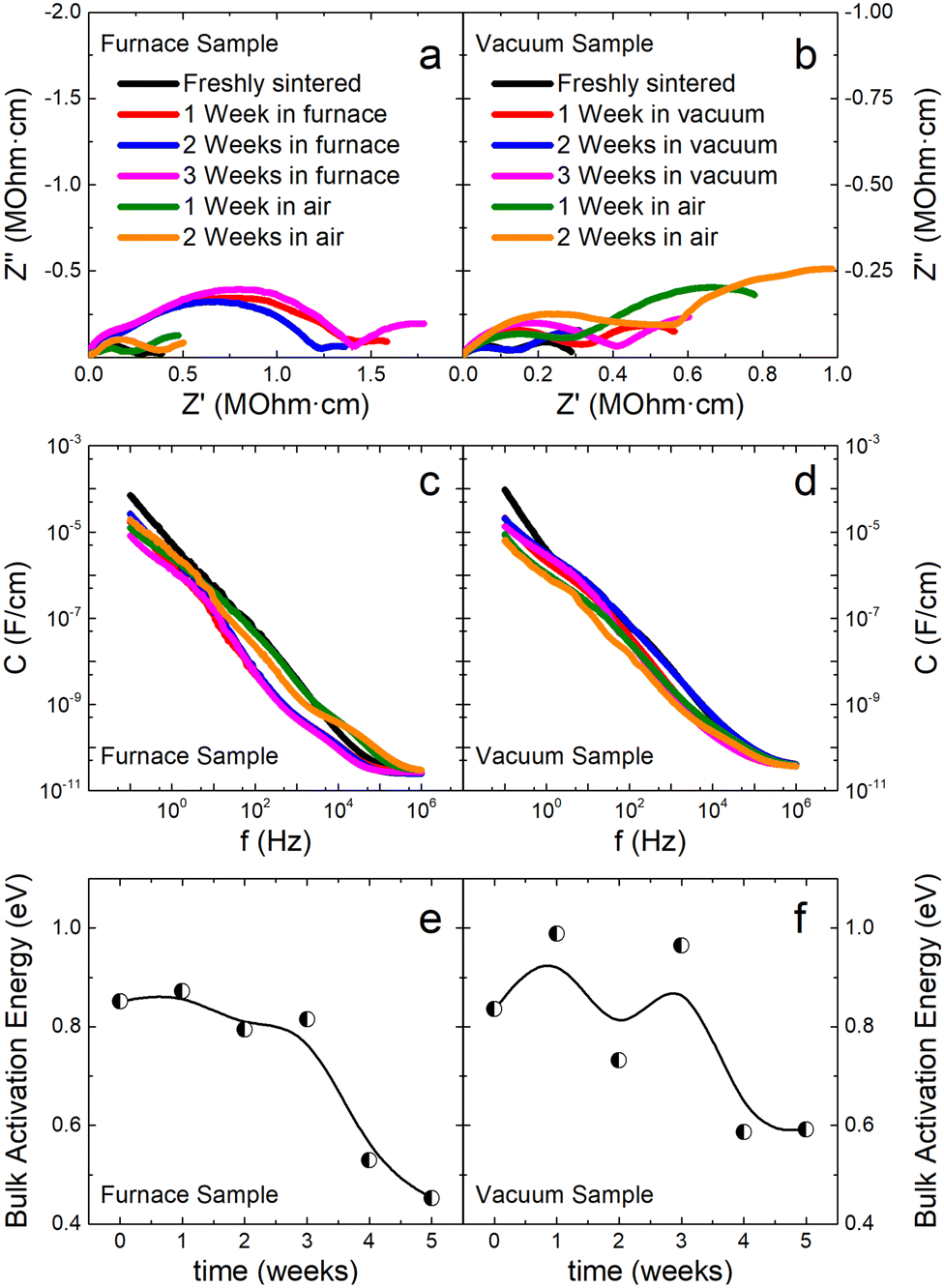 | ||
| Fig. 6 Time evolution of (a) and (b) Nyquist plots, (c) and (d) capacitance versus frequency response, and (e) and (f) activation energy for bulk conduction of a CCFS sample under a quadratic current profile. The sample is cut in two halves after sintering; one is kept in vacuum and the other in a furnace at 800 °C for three weeks. After that, both halves are stored in ambient atmosphere and measured at one-week intervals for two weeks. Measurements were performed at 350 °C. | ||
If the formation of oxygen vacancies was the only underlying mechanism responsible for the FINA effect, the sample held in the furnace for three weeks should reoxygenate rapidly and be stable with time but instead tends to become conductive again after the treatment. Otherwise, the sample held in vacuum should favor the formation of oxygen vacancies until saturated, but it has a non-trivial time dependence. Consequently, we hypothesize that the FINA process has two underlying mechanisms: (i) a short-range one responsible for the oxygen vacancies formation and increase of conductivity during the first weeks after sintering, and (ii) a long-range one related to the annihilation of the same defects. In order to probe this hypothesis, impedance spectroscopy measurements for both samples after remaining 9 months in ambient atmosphere are performed. As shown in Fig. 7, the resistivity of both samples significantly improves while the capacitance decreases several orders of magnitude for all frequency spectrums.
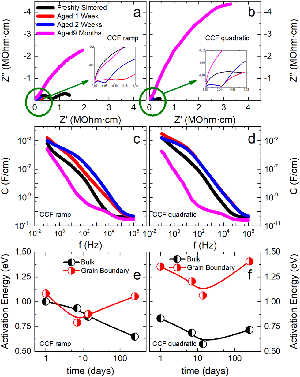 | ||
| Fig. 7 (a) and (b) Time evolution of Nyquist plots, (c) and (d) capacitance versus frequency response, and (e) and (f) activation energy for conduction of CCFS samples under two different current profiles. Measurements were carried out at 350 °C. | ||
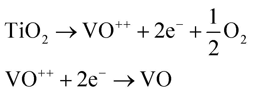
Even though the long-range mechanism of the FINA seems to be the normal recombination of oxygen vacancies, the short-range mechanism is still not fully understood. We speculate that due to higher reactivity, samples obtained from nanopowders tend to reduce during sintering following the reactions:
4. Conclusions
This work discusses the influence of the starting powder over the flash-sintered sample behavior during and after sintering. We selected BaTiO3 since it is a well-known perovskite-structured ferroelectric archetype. As already reported, submicron powders require less energy to densify, but we observed the time evolution of the sample properties towards becoming electronically conductive at room temperature. This abnormal behavior is accompanied by a highly inhomogeneous microstructure, which can be exhaustively tuned using a proper electric current profile during flash sintering, providing a new pathway to tailor the microstructure. While the origin of the properties’ evolution is not fully understood, the results evidence that lattice reduction and oxygen vacancies play a crucial role. The formation of these defects seems to be enhanced when using submicron powders, which until now were thought to be able to achieve better results in flash sintering experiments.Author contributions
Samuel Lopez-Blanco: conceptualization, methodology, formal analysis, investigation, resources, visualization, writing – original draft. Xavier Vendrell: methodology, formal analysis, visualization, writing – review & editing. Lourdes Mestres: validation, project administration. Diego A. Ochoa: validation, investigation, formal analysis. Jose E. Garcia: conceptualization, methodology, visualization, writing – review & editing, supervision, project administration, funding acquisition.Conflicts of interest
There are no conflicts to declare.Acknowledgements
This work was supported by the Agencia Estatal de Investigación (AEI), Spain, project PGC2018-099158-B-I00. S. L-B. thanks Agència de Gestió dAjuts Universitaris i de Recerca (AGAUR), Catalonia, Spain, for the FI-SDUR contract (2020 FISDU 00489). The authors acknowledge the ESRF (The European Synchrotron) for provision of synchrotron radiation facilities, and we would like to thank the SpLine-BM25 staff for assistance in using the beamline.Notes and references
- M. Cologna, B. Rashkova and R. Raj, J. Am. Ceram. Soc., 2010, 93, 3556–3559 CrossRef CAS.
- J. Luo, Scr. Mater., 2018, 146, 260–266 CrossRef CAS.
- H. Charalambous, S. K. Jha, K. H. Christian, R. T. Lay and T. Tsakalakos, J. Eur. Ceram. Soc., 2018, 38, 3689–3693 CrossRef CAS.
- R. Todd, E. Zapata-Solvas, R. Bonilla, T. Sneddon and P. Wilshaw, J. Eur. Ceram. Soc., 2015, 35, 1865–1877 CrossRef CAS.
- M. Cologna, J. S. Francis and R. Raj, J. Eur. Ceram. Soc., 2011, 31, 2827–2837 CrossRef CAS.
- R. Raj, A. Kulkarni, J.-M. Lebrun and S. Jha, MRS Bull., 2021, 46, 36–43 CrossRef CAS.
- C. Dancer, Mater. Res. Express, 2016, 3, 102001 CrossRef.
- M. Biesuz and V. M. Sglavo, J. Eur. Ceram. Soc., 2019, 39, 115–143 CrossRef CAS.
- J.-C. MPeko, J. S. Francis and R. Raj, J. Eur. Ceram. Soc., 2014, 34, 3655–3660 CrossRef CAS.
- R. Shi, Y. Pu, W. Wang, Y. Shi, J. Li, X. Guo and M. Yang, Ceram. Int., 2019, 45, 7085–7089 CrossRef CAS.
- X. Su, G. Bai, Y. Jia, Z. Wang, W. Wu, X. Yan, T. Ai, P. Zhao and L. Zhou, J. Eur. Ceram. Soc., 2018, 38, 3489–3497 CrossRef CAS.
- Y. Wu, X. Su, G. An and W. Hong, Scr. Mater., 2020, 174, 49–52 CrossRef CAS.
- A. Taibi, S. Chaguetmi, P. E. Sánchez-Jiménez, A. Perejón, J. E. Garca, H. Satha and L. A. Pérez-Maqueda, Ceram. Int., 2021, 47, 26947–26954 CrossRef CAS.
- V. Buscaglia and C. A. Randall, J. Eur. Ceram. Soc., 2020, 40, 3744–3758 CrossRef CAS.
- M. Acosta, N. Novak, V. Rojas, S. Patel, R. Vaish, J. Koruza, G. Rossetti Jr and J. Rödel, Appl. Phys. Rev., 2017, 4, 041305 Search PubMed.
- J. Gao, D. Xue, W. Liu, C. Zhou and X. Ren, Actuators, 2017, 24 CrossRef CAS.
- S. López-Blanco, D. A. Ochoa, X. Vendrell, L. Mestres and J. E. Garca, J. Eur. Ceram. Soc., 2022, 42, 5669–5674 CrossRef.
- J. S. Francis, M. Cologna and R. Raj, J. Eur. Ceram. Soc., 2012, 32, 3129–3136 CrossRef CAS.
- K. Wu and W. A. Schulze, J. Am. Ceram. Soc., 1992, 75, 3390–3395 CrossRef CAS.
- J. T. Irvine, D. C. Sinclair and A. R. West, Adv. Mater., 1990, 2, 132–138 CrossRef CAS.
- Y. Dong and I.-W. Chen, J. Am. Ceram. Soc., 2015, 98, 3624–3627 CrossRef CAS.
- R. D. Levi and Y. Tsur, Adv. Mater., 2005, 17, 1606–1608 CrossRef CAS.
- S. Tsunekawa, S. Ito, T. Mori, K. Ishikawa, Z.-Q. Li and Y. Kawazoe, Phys. Rev. B: Condens. Matter Mater. Phys., 2000, 62, 3065 CrossRef CAS.
- S. Tsunekawa, K. Ishikawa, Z.-Q. Li, Y. Kawazoe and A. Kasuya, Phys. Rev. Lett., 2000, 85, 3440 CrossRef CAS PubMed.
- S. K. Upadhyay, V. R. Reddy, K. Sharma, A. Gome and A. Gupta, Ferroelectrics, 2012, 437, 171–180 CrossRef CAS.
- V. P. Pavlović, M. V. Nikolić, V. B. Pavlović, N. Labus, L. Živković and B. D. Stojanović, Ferroelectrics, 2005, 319, 75–85 CrossRef.
- G. Lewis, C. Catlow and R. Casselton, J. Am. Ceram. Soc., 1985, 68, 555–558 CrossRef CAS.
- A. R. West, Solid state chemistry and its applications, John Wiley & Sons, 2022, pp. 359–362 Search PubMed.
- J. Jamnik and J. Maier, J. Electrochem. Soc., 1999, 146, 4183 CrossRef CAS.
- A. Uehashi, H. Yoshida, T. Tokunaga, K. Sasaki and T. Yamamoto, J. Ceram. Soc. Jpn., 2015, 123, 465–468 CrossRef CAS.
- W. Ji, B. Parker, S. Falco, J. Zhang, Z. Fu and R. Todd, J. Eur. Ceram. Soc., 2017, 37, 2547–2551 CrossRef CAS.
- P. Kumar MK, D. Yadav, J.-M. Lebrun and R. Raj, J. Am. Ceram. Soc., 2019, 102, 823–835 CrossRef CAS.
- I. R. Lavagnini, J. V. Campos, J. A. Ferreira and E. M. A. Pallone, J. Am. Ceram. Soc., 2020, 103, 3493–3499 CrossRef CAS.
- K. Ren, S. Huang, Y. Cao, G. Shao and Y. Wang, Scr. Mater., 2020, 186, 362–365 CrossRef CAS.
- D. Glower and R. Heckman, J. Chem. Phys., 1964, 41, 877–879 CrossRef CAS.
- H.-I. Yoo, C.-R. Song and D.-K. Lee, J. Electroceram., 2002, 8, 5–36 CrossRef CAS.
- S. Lee, Z.-K. Liu, M.-H. Kim and C. A. Randall, J. Appl. Phys., 2007, 101, 054119 CrossRef.
- B. Li, X. Wang, L. Li, H. Zhou, X. Liu, X. Han, Y. Zhang, X. Qi and X. Deng, Mater. Chem. Phys., 2004, 83, 23–28 CrossRef CAS.
- Y. Park, K. Cho and H.-G. Kim, Mater. Res. Bull., 1997, 32, 1485–1494 CrossRef CAS.
- J. A. Dawson, Phys. Status Solidi b, 2020, 257, 1900422 CrossRef CAS.
- J. Fujioka, A. Doi, D. Okuyama, D. Morikawa, T. Arima, K. Okada, Y. Kaneko, T. Fukuda, H. Uchiyama and D. Ishikawa, et al. , Sci. Rep., 2015, 5, 13207 CrossRef CAS PubMed.
- J. Narayan, Scr. Mater., 2013, 68, 785–788 CrossRef CAS.
- J. Narayan, Scr. Mater., 2020, 176, 117–121 CrossRef CAS.
- M. Buscaglia, V. Buscaglia, M. Viviani, P. Nanni and M. Hanuskova, J. Eur. Ceram. Soc., 2000, 20, 1997–2007 CrossRef CAS.
- J. Li, J. Cho, J. Ding, H. Charalambous, S. Xue, H. Wang, X. L. Phuah, J. Jian, X. Wang and C. Ophus, et al. , Sci. Adv., 2019, 5, eaaw5519 CrossRef CAS PubMed.
- J. Cho, Q. Li, H. Wang, Z. Fan, J. Li, S. Xue, K. Vikrant, H. Wang, T. B. Holland and A. K. Mukherjee, et al. , Nat. Commun., 2018, 9, 2063 CrossRef PubMed.
- X. Su, Z. Jiao, M. Fu, G. An, Y. Wu, Q. Tian, P. Xu, W. Wu, X. Chang and J. Liu, Int. J. Appl. Ceram. Technol., 2021, 18, 1999–2009 CrossRef CAS.
- M. Jongmanns, R. Raj and D. E. Wolf, New J. Phys., 2018, 20, 093013 CrossRef.
- M. Jongmanns and D. E. Wolf, J. Am. Ceram. Soc., 2020, 103, 589–596 CrossRef CAS.
- B. Yoon, D. Yadav, R. Raj, E. Sortino, S. Ghose, P. Sarin and D. Shoemaker, J. Am. Ceram. Soc., 2018, 101, 1811–1817 CrossRef CAS.
- P. Maldonado, K. Carva, M. Flammer and P. M. Oppeneer, Phys. Rev. B: Condens. Matter Mater. Phys., 2017, 96, 174439 CrossRef.
Footnote |
| † Electronic supplementary information (ESI) available. See DOI: https://doi.org/10.1039/d3tc02143b |
| This journal is © The Royal Society of Chemistry 2023 |