
 Open Access Article
 This Open Access Article is licensed under a
 Creative Commons Attribution 3.0 Unported Licence
Blocking wide bandgap mixed halide perovskites’ decomposition through polymer inclusion†
Francesco
Bisconti
 a,
Mauro
Leoncini
a,
Gianluca
Bravetti
ab,
Antonella
Giuri
a,
Laura
Polimeno
a,
Sonia
Carallo
a,
Silvia
Colella
c,
Lorenzo
Gatto
de,
Federico
Grandi
de,
Eugenio
Cinquanta
e,
Caterina
Vozzi
e,
Salvatore
Gambino
a,
Lorenzo
Dominici
*a and
Aurora
Rizzo
*a
a,
Mauro
Leoncini
a,
Gianluca
Bravetti
ab,
Antonella
Giuri
a,
Laura
Polimeno
a,
Sonia
Carallo
a,
Silvia
Colella
c,
Lorenzo
Gatto
de,
Federico
Grandi
de,
Eugenio
Cinquanta
e,
Caterina
Vozzi
e,
Salvatore
Gambino
a,
Lorenzo
Dominici
*a and
Aurora
Rizzo
*a
aCNR NANOTEC – Istituto di Nanotecnologia, c/o Campus Ecotekne, Via Monteroni, 73100 Lecce, Italy. E-mail: lorenzo.dominici@nanotec.cnr.it; aurora.rizzo@nanotec.cnr.it
bDepartment of Mathematics and Physics “E. De Giorgi”, University of Salento, Campus Ecotekne, via Arnesano, 73100 Lecce, Italy
cCNR NANOTEC – Istituto di Nanotecnologia, c/o Dipartimento di Chimica, Università di Bari, Via Orabona 4, 70126 Bari, Italy
dDipartimento di Fisica, Politecnico di Milano, Piazza Leonardo da Vinci, 20133 Milano, Italy
eCNR IFN – Istituto di Fotonica e Nanotecnologie, Piazza Leonardo da Vinci 32, 20133 Milano, Italy
First published on 3rd August 2023
Abstract
The relatively easy tunability of perovskites’ energy gap, as well as the synthesis of mixed halide perovskites, make them highly versatile and compatible with others semiconductor materials to produce efficient tandem solar cells. However, one of the obstacles holding back the development of this technology is the poor photostability of perovskite, one of the most critical aspects of mixed halide formulations. In this work, we use a polymeric additive to improve the photostability of halide perovskites. We developed a polymer-mediated crystallization (PMC) perovskite that allowed obtaining solar cells with photovoltaic performances equal to reference perovskites (power conversion efficiency ∼17%) but with superior endurance to light exposure, demonstrated by a laser-induced photostability assessment. Furthermore, by photoluminescence mapping and terahertz spectroscopy we carried out an in-depth investigation of the photodegradation process, revealing that in PMC perovskite, halogen segregation effects can still take place but are confined to spatially limited regions of the sample.
Introduction
Metal halide perovskite semiconductors have emerged among the leading candidates for the next generation of solar cells thanks to their excellent photovoltaic performance combined with simple manufacturing processes.1–3 The recent integration of wide-bandgap perovskite solar cells (PSCs) in perovskite/perovskite, perovskite/Si, and perovskite/CIGS tandem devices can in principle result in very high power conversion efficiency (PCE).4–7 This design indeed can better harness solar energy, since both the high- and low-energy photons can be complementarily absorbed by the wide- and low-bandgap top and bottom subcells, eventually overcoming the Shockley–Queisser limit.8–11 To be efficiently integrated into a tandem device, the perovskite top cells should feature a bandgap in the range of ∼1.6–1.8 eV, which depends upon the characteristic bandgap of the bottom subcell. Although widening the bandgap of perovskite materials through I–Br halogen mixing is rather simple, there are still significant issues related to the inherent instability of mixed halide compositions. Besides the combined effects of moisture and light illumination, which can induce a rapid chemical and structural modification in perovskite materials, light-induced halide segregation also happens when Br content is above 20%.12–19Several works have studied and proposed methods to improve mixed halide perovskite stability or suppress halide segregation. An improvement of the stability against photoinduced halide segregation by the compression of MAPb(I1−xBrx)3 film applying external pressure or reducing the cation size has been demonstrated.20 Regarding the cation site, a higher methylammonium (MA+) content was revealed to speed up the degradation, whereas the partial substitution with formamidium (FA+) could benefit from an increased energetic barrier for halide segregation.21 McGehee's group also developed a more stable perovskite, suitable for the tandem application, by the suppression of the phase segregation developing a triple-halide formulation.6 Other approaches to increase photostability reside in the use of small molecules and polymers as additives. Ethylenediamine inclusion into perovskite precursors was found to be useful to improve the photovoltaic performance and the material stability,22 as well as a coating layer of poly(methyl methacrylate) (PMMA) was successfully used to the scope.23 For this reason, considering the importance that perovskite-Si tandem solar cells represent in the scenario of photovoltaic technology and in light of the problems related to material stability in terms of photodegradation and phase segregation, we sought to exploit our experience with the use of polymers as cooperative agents to control the crystallisation of perovskite films24–26 to tackle the stability issues. Therefore, we have selected Gellan Gum as a polymeric not toxic additive to stabilize the perovskite structure and to improve its photostability. The choice of this material was driven by our previous studies with similar polysaccharides where we were able to obtain a better processability25 and increased thermal stability,24,27,28 exploiting the capability of these polymers to interact via hydroxyl functionalities with the perovskite organic cations already in the precursors’ solutions. Moreover, Gellan Gum is a gelling agent and is capable to modify the perovskite precursors’ solution rheology. The combined effect of enhanced precursors’ ink viscosity and the interaction with the organic cation precursors allows to interfere with the crystallization process and to obtain a compact and homogenous morphology via a single-step coating, as already observed for other polysaccharides.29–31 In this work, we exploit Gellan Gum polysaccharide to obtain mixed halide perovskite films with a reduced photodegradation without disturbing the photovoltaic performance. At the same time, an in-depth investigation was conducted to study the dynamics involved in the degradation process.
Material development and device implementation
Considering the proportional bandgap's blueshift with the bromine content, several formulations of wide band gap perovskite were developed varying the bromine concentration in a MAPb(I1−xBrx) perovskite. The values of the optimized energy gap for efficient Perovskite/Si tandem solar cells can be obtained with 10–20% of Br,11 while perovskites with higher Br concentration are generally used as a model to study the phenomena behind the photoinstability.32Here, we first produced reference mixed I–Br perovskites according to literature,33 MAPb(I1−xBrx)3 perovskites with x = 0, 0.1, 0.2, 0.3, 0.4, 1. Then, we realize the same formulations with the addition of Gellan Gum (chemical structure in Fig. 1a).
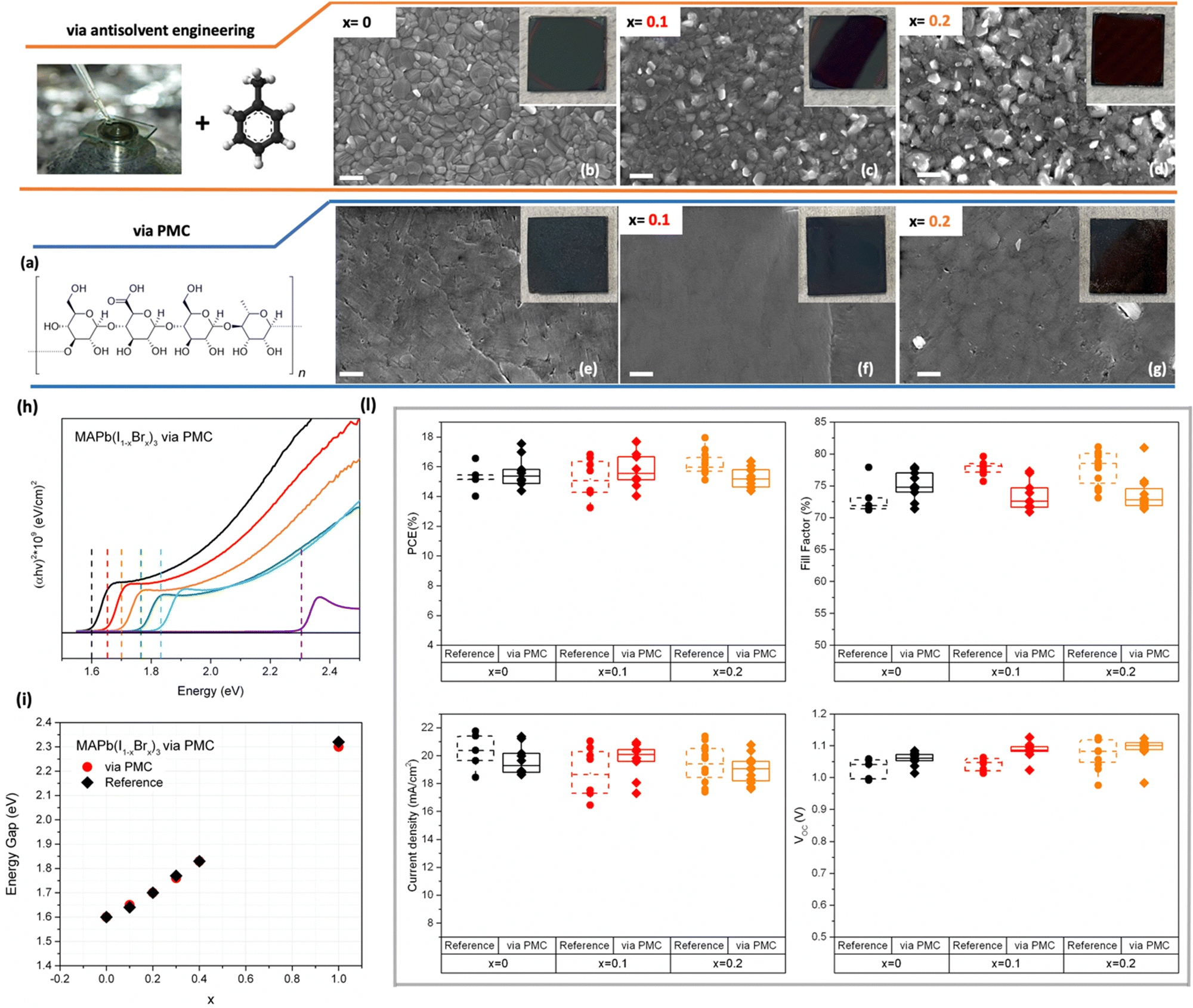 | ||
Fig. 1 From perovskite morphology to device integration. (a) Gellan Gum chemical structure. SEM analysis reference MAPb(I1−xBrx)3 perovskite formulations at Br concentration (b) x = 0, (c) x = 0.1, (d) x = 0.2 and corresponding (e) x = 0, (f) x = 0.1, (g) x = 0.2 perovskite obtained via polymer mediated crystallization. Scale bar 300 nm. (h–i) Energy gap of each formulation based on the different I![[thin space (1/6-em)]](https://www.rsc.org/images/entities/char_2009.gif) :Br ratio determined by applying the Tauc Plot method (vertical dot lines to facilitate the readability). (l) Statistic comparison of photovoltaic parameters recorded from devices based on reference and via PMC perovskite with different Br concentrations. :Br ratio determined by applying the Tauc Plot method (vertical dot lines to facilitate the readability). (l) Statistic comparison of photovoltaic parameters recorded from devices based on reference and via PMC perovskite with different Br concentrations. | ||
Reference perovskites were deposited via antisolvent engineering obtaining perovskite films with a homogenous morphology, except for x = 0.4 that show the presence of some pinholes. (Fig. 1b–d and Fig. S1, S2, ESI†). At the same time, we optimized the deposition of MAPb(I1−xBrx)3via polymer-mediated crystallization (via PMC), where the use of the polymer as a rheological modifier allows avoiding the use of the additional antisolvent dripping step. Based on this approach, we achieved perovskite films that exhibited a good morphology with bigger and uniform perovskite grains (Fig. 1e–g and Fig. S3, S4, ESI†) and suitable crystallographic features, ideal to allow good results in terms of power conversion efficiency of the complete device. About the latter, we carried out an X-ray diffractometric (XRD) analysis on perovskite films to evaluate if a desired crystallization process took place despite the absence of the antisolvent step, generally used for proper control of the perovskite crystal growth, and if the conversion to perovskite phase is completed. XRD analysis revealed a slightly slower crystallization, from the residual presence of peaks related to the precursor's intermediates at 2 Theta = 6.6°, 7.2°, 9.2°. Hence, we protracted the annealing step from 30 min to 45 min obtaining the complete conversion from precursors to perovskite (Fig. S5–S7, ESI†).
The absorption spectra of the reference perovskite and that obtained PMC perovskite were acquired and the optical Energy Gap (Eg) was calculated by the Tauc plot equation (Fig. 1h–i). The reference perovskite Eg was also calculated (Fig. S8 and S9, ESI†). They show the typical proportional blueshift induced by the increasing Br content. Once we confirmed the good quality of the perovskite film, we fabricated p–i–n architecture-based solar cells (see ESI†). The overall photovoltaic parameters reported in Fig. 1l show that the via PMC approach allows reaching similar performance to the reference perovskite, also when varying the I–Br ratio from x = 0 to x = 0.2. The numerical data of best and average performance are reported in Fig. S10 (ESI†), while the maximum power point and the incident photon to current efficiency of reference and PMC x = 0.2 perovskite were also analyzed and shown in Fig. S11 (ESI†). Interestingly, via PMC, in particular devices with x = 0.1 and x = 0.2 perovskite revealed a clear improvement of the Voc values if compared to the reference perovskite. This result could be explained by considering the morphology of the PMC perovskite that is characterised by large and compact grains, which is recognised as one of the essentials factors to achieve higher Voc values. Morphology that also plays a key role in the photostability of the perovskite material.34 Nonetheless a reduction of the FF and Jsc can be also noticed via PCM that can be attributed to the insulating nature of the GG polymers.35
Photostability and halide-segregation
Despite the remarkable performance allowed by perovskite, the material suffers from stability issues that affect the lifespan of the entire photovoltaic device. Extrinsic factors, mainly environmental like oxygen, light, and humidity, as well as intrinsic factors like ion migration, cause the degradation of the perovskite.36 In particular, light has a strong impact on mixed halide perovskites where decomposition of the perovskite takes place due to the halide segregation phenomenon.37 To study the photostability of the perovskite, we first measured the photoluminescence (PL) after light exposure. The samples were irradiated at a wavelength of 500 nm by a pulsed laser source with a frequency of 20 Hz and width of 7 ns with an average power of 8.4 mW, keeping the exposure on for 2 hours and the PL measurements were acquired every 20 minutes, exciting the sample at 430 nm with a power of 2.4 mW. The measurements were carried out illuminating an area of 3 mm2.The analysis of the photoaging of the x = 0.4 samples (Fig. 2) showed that the reference perovskite is affected by a strong blueshift in the PL spectra compared to the PMC perovskite (unnormalized data in Fig. S12, ESI†). This phenomenon has never been observed for polycrystalline perovskite films, but was previously observed for perovskite nanocrystals, albeit under continuous illumination.38 The authors explained this blue shift phenomenon by considering that the Pb–Br bond is shorter and stronger than the Pb–I bond. Thus, upon laser excitation, the Pb–I bond is disrupted, leading to the formation of Br-rich domains and thus a blueshifted emission, which is reversible. In our case, the reported blueshift was only observed for the reference mixed halide perovskite and it was obtained upon pulsed laser irradiation. We have found that this process is not reversible, (see Fig. S13, ESI†) so we have attributed it to a photodegradation phenomenon, which needs to be further investigated. The absence of this blue shift in the perovskite with gellan gum suggests a better stability of the material, which could be due to a more compact morphology of the perovskite films via PMC. This better stability is also consistent with the generally better robustness of the perovskite-polymer composite to stress factors such as heat, moisture or light.38,39 The incorporation of polysaccharide into perovskite can indeed mitigate the decomposition of volatile MA cation and iodine species, limiting further degradation.35
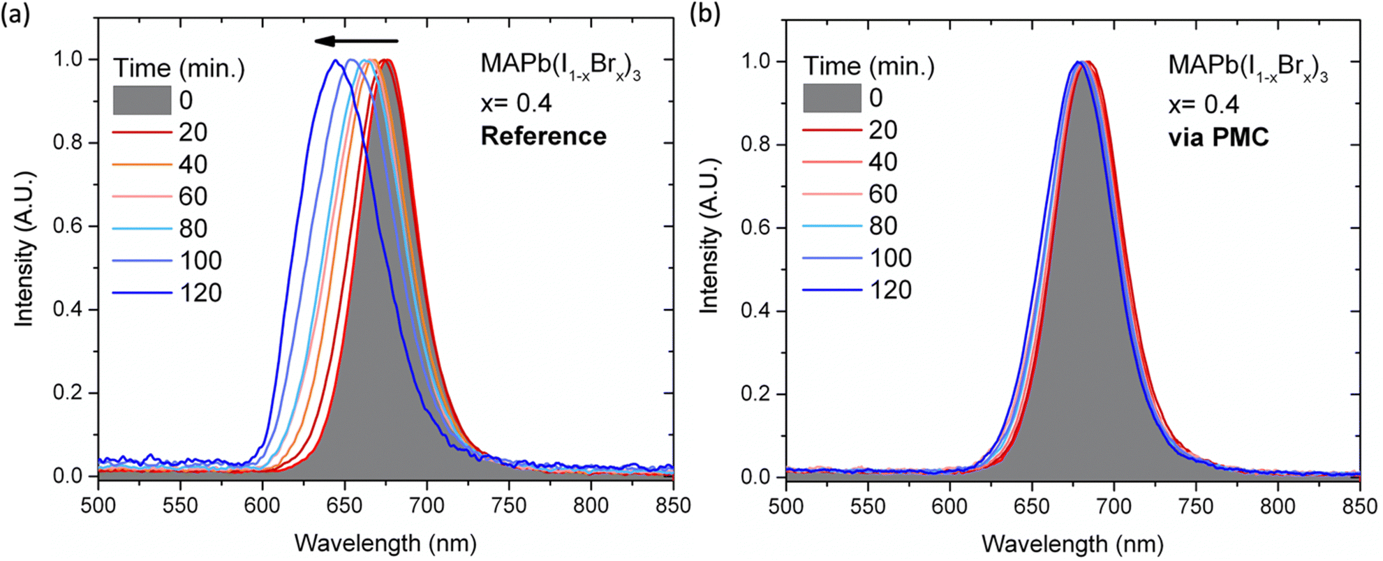 | ||
| Fig. 2 Laser-induced photo-instability assessment. Reference and via PMC MAPb(I1−xBrx)3 films at x = 0.4 irradiated with a 500 nm pulsed laser. The PL spectra acquired at steps of 20 minutes show that the (a) neat perovskite undergoes a deep blueshift of the emission compared to the (b) perovskite obtained via PMC. | ||
We then evaluated if the polymer stabilization could positively also influence the phase segregation. Photoluminescence measurements under continuum light at a wavelength of 385 nm were carried out acquiring each spectrum after 2.5 s for 130 s. For both samples, the reference and PMC perovskites, we observed a redshift in the PL emission (Fig. 3a and b, respectively), which is related to the well-known halide segregation phenomenon,15,17 leading to I-rich domains. This redshift is reversible (Fig. S14, ESI†), following halide segregation effects, in opposition to the irreversible blueshift observed under pulsed laser light, ascribed to photo-degradation, and inhibited by the Gellan Gum. From the PL redshift shown in Fig. 3, we concluded that the PMC method is not able to block the segregation effects. However, we can note a different ratio of the amplitudes among the long-time redshifted peaks and the early-time original peaks, in the reference and PMC cases. The latter case shows a lesser relative enhancement of the peak in time (Fig. S15, ESI†). This may indicate different segregation effects in the two materials. For a deeper analysis of the samples and the modifications induced by light exposure, we perform a mapping of the photoluminescence.
 | ||
| Fig. 3 Laser-induced phase segregation assessment. PL measurements under a continuum light illumination at a wavelength of 385 nm for (a) reference and (b) via PMC perovskites films. PL spectra were acquired for 130 seconds at steps of 2.5 s. | ||
Hyperspectral photoluminescence maps
We performed a spectrally resolved imaging of the photoluminescence on different samples, after keeping the films exposed to continuous wave (CW) light for inducing the segregation effect. The optical images (white light reflection) and single-line emission PL maps of the MAPb(I1−xBrx)3 films at x = 0.2 appear in the first part of Fig. 4, both for the reference (Fig. 4a–c) and the via PMC perovskite (Fig. 4d–f). When looking at the optical images, it is possible to see a larger sizing of the structures or grains in the case of the Gellan Gum adjuvanted fabrication (compare Fig. 4d with Fig. 4a). Such larger structures are also visible in the PL map obtained at the emission wavelength close to that of the original phase (730 nm, corresponding to Fig. 4b and e). However, at a longer wavelength (770 nm, in Fig. 4c and f) some spatially confined features appear in the PMC case that can in principle be associated with more localized segregation.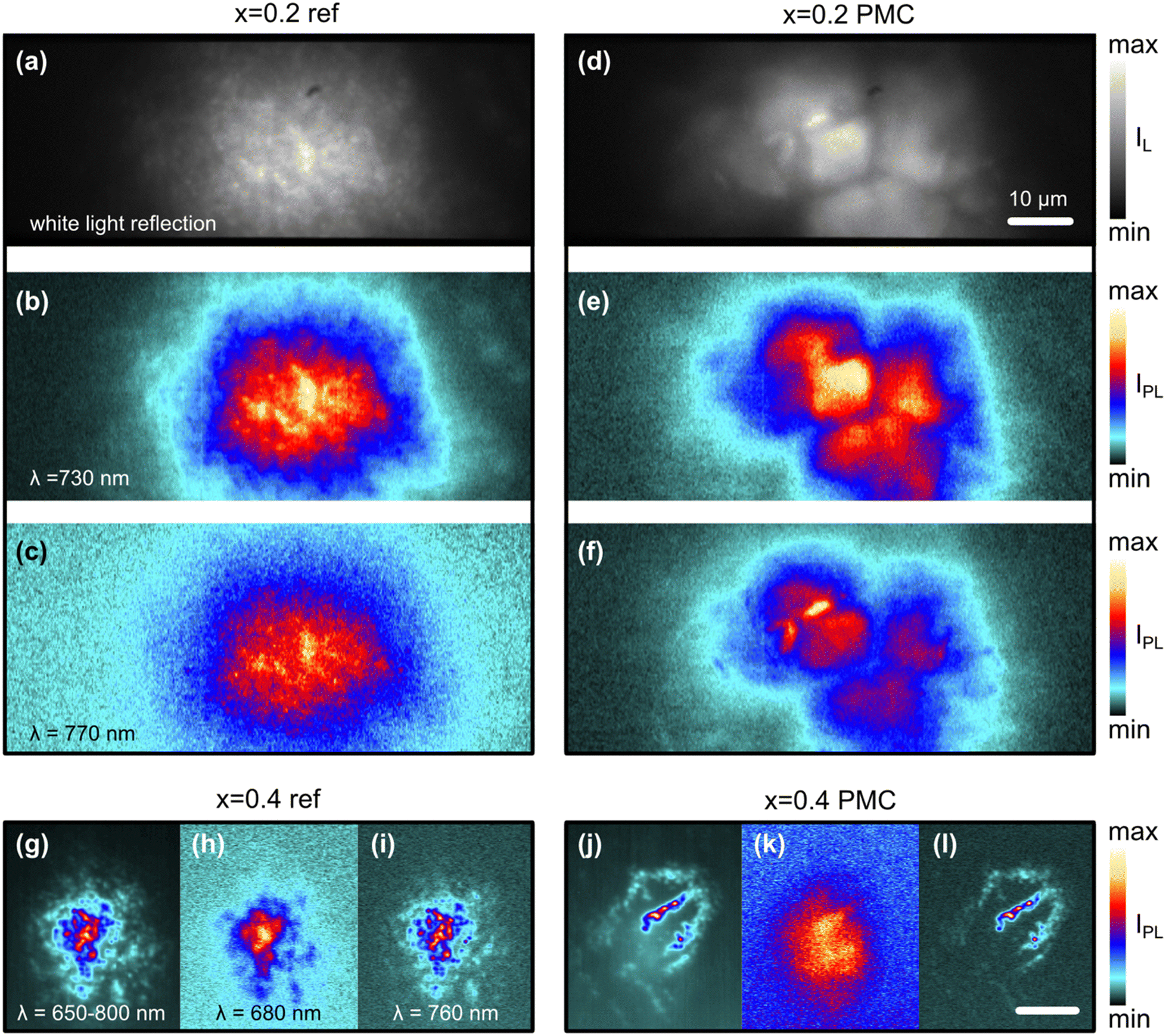 | ||
| Fig. 4 Hyperspectral photoluminescence maps and opticals images. Optical image of reference perovskite at Br concentration of x = 0.2 (a) and corresponding single-line PL emission at 730 nm and 770 nm (b) and (c). Optical image of PMC perovskite at x = 0.2 (d), and corresponding single-line PL emission at 730 nm and 770 nm (e) and (f). The optical images are taken under white light reflection, the boundaries of the entrance slit appear as two dark stripes in the top and bottom parts of panels (a) and (d). Reference perovskite at Br concentration of x = 0.4 (g), (h) and (i) and corresponding PMC perovskite at x = 0.4 (j)–(l), imaged at a PL emission integrated in the 650–800 nm (g) and (j) and at single-line PL emission of wavelength 680 nm (h) and (k) and 760 nm (i) and (l). The scale bar is 10 μm across all the panels. | ||
The trend is even more evident in the case of a Br content x = 0.4 (Fig. 4g–l). Here we used as a comparison image the wavelength resolved PL emission, integrated in the 650–800 nm interval (new panels Fig. 4g and j). In this case, it is possible to see that the PL emission at the higher wavelength is a footprint of the localized features of the area morphology, while the shorter wavelength emission is more delocalized across the whole area. In fact, we could use more separated observational wavelengths to compare the different phases. We used the original peak wavelength as also seen from the spectra of Fig. 3 to observe a more or less uniform original phase in both references and via PMC perovskites (680 nm, in Fig. 4h and k). However, at the longer wavelengths close to the peak of the segregated phase (760 nm, in Fig. 4i and l), the PMC perovskite shows highly localized emission (Fig. 4l) with respect to the reference perovskite (Fig. 4i). Upon comparing the PL maps to the SEM microphotographs of the perovskite films at x = 0.4 (see ESI†), we observed similarly sized structures. From the hyperspectral maps, we hence deduced that the PMC helps to have larger and smoother crystalline grains, where the segregation is also hindered. Furthermore, the residual grain boundaries and other defects act as localized areas of enhanced segregation. The reduced area affected by the segregation may be also correlated with the smaller relative increase of the associated peaks’ intensity during irradiation in the PMC case in Fig. 3.
Terahertz spectroscopy
To gain further insight into the phase-segregation process in the perovskite films, we performed a terahertz time-domain spectroscopic (THz-TDS) characterization of the reference sample of MAPb(I1−xBrx)3 with x = 0.4, following the approach proposed in the literature.40 The real part of the conductivity, retrieved by a thin-film approximation41 (using an estimated film thickness of 300 nm, based on a previous statistical calibration of the fabrication protocol), is shown by the blue circles in Fig. 5 (pre-exposure). We repeated the measurement in different positions of the sample (Fig. 5a and b) and we obtained good agreement between the spectra and the THz spectrum previously reported by Motti et al.40 In particular, the frequencies of the two absorption features are in good agreement with the literature, while the amplitude value depends on the estimated thickness of the sample in the specific position. We then exposed the sample to continuous radiation at a wavelength of 532 nm (average power of 0.1 W) for 20 minutes and, keeping the 532 nm laser on, we repeated the THz-TDS characterization. The results (represented by the green triangles in Fig. 5a) indicate a significant increase in absorption at higher frequencies.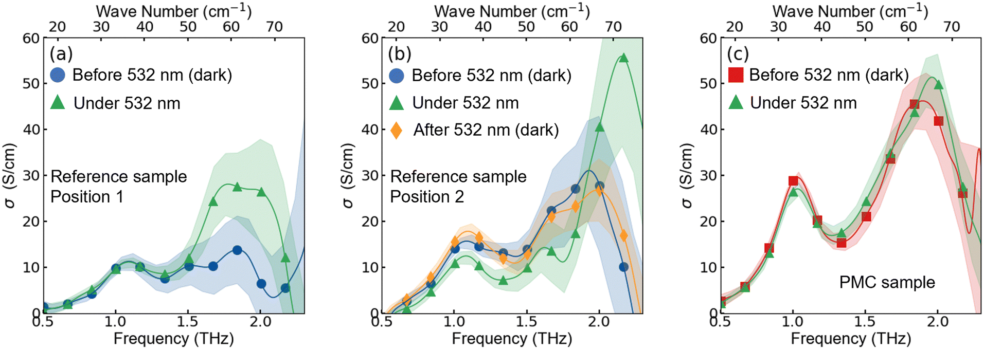 | ||
| Fig. 5 Terahertz spectroscopy. THz static conductivity spectra (real part). (a) x = 0.4 reference sample (position 1) before (blue circles) and during (green triangles) the exposure to cw 532 nm radiation. (b) x = 0.4 reference sample (position 2) before (blue circles) and during (green triangles) the exposure to cw 532 nm. The measurement was repeated after switching off the 532 nm light and leaving the sample for 30 minutes in the dark (orange diamonds). (c) x = 0.4 PMC sample before (red squares) and during (green triangles) the exposure to cw 532 nm. To compute the conductivity we used the estimated thickness of 300 nm for the reference sample (a) and (b) and 400 nm for the PMC sample (c). | ||
Following the same procedure, we repeated the characterization in the second position of the sample, and we obtained the results represented in Fig. 5b, with the same colour code (blue circles for pre-exposure and green triangles for the exposed sample). The differences between Fig. 5a and b can be attributed to a spatial non-uniformity of the perovskite film. It should be noticed that the 532 nm radiation can photoexcite charge carriers above the bandgap of the x = 0.4 samples (1.83 eV according to Fig. 1i and Fig. S9, ESI†) and the THz measurements are performed in a condition of dynamical equilibrium set by the cw charge injection together with the recombination inside the material. Using the rate constants reported from ref. 40 and representative optical parameters at 532 nm of A. Ishteev et al.,42 we numerically solved the rate equation with a cw power of 0.1 W over a spot diameter of 5 mm obtaining a steady-state carrier density of 1 × 1014 cm−3. Given a mobility of 37 cm2 V−1 s−1,38 this carrier density corresponds approximately to a DC conductivity of 8 × 10⁻⁴ S cm−1. This contribution cannot explain a photoinduced change of the order of S cm−1 or larger. Moreover, its effect should be a higher real part of the conductivity at all the frequencies, according to the Drude or Drude-Smith models. Instead, in Fig. 5a the conductivity strongly increases only in a specific interval between 1.5 and 2.2 THz. In Fig. 5b we even see a smaller conductivity below 2 THz, while we observe the opposite trend only above 2 THz. We propose instead that the dominant change comes from the modification of the lattice as a consequence of the halide segregation phenomenon. This is indeed a photoinduced modification of the lattice and can correspond to a different infrared activity and a consequent change of the response function in the far-IR. In the second position on the reference sample, we also measured the response after switching off the 532 nm radiation and waiting for 30 minutes. The results (corresponding to the orange diamonds in Fig. 5b) indicate the recovery of the original static THz response. This means that the observed photo-alteration of the THz response is a reversible process and corroborates its relationship with the halide segregation. Nevertheless, a similar change of the static response was not reported in literature,40 where the signature of the halide segregation was instead the appearance of a signal in a 700 nm pump – THz probe experiment. The reason for the different outcome of our static measurements after the segregation could be the larger area that we exposed to the 532 nm cw beam. This could open a new route to investigate the effects of the halide segregation process. We completed our measurements with an 800 nm pump – THz probe experiment, but we did not detect any signal after the exposure to the 532 nm radiation and we attribute this to the lower pump photon energy. We used the same procedure to study the x = 0.4 perovskite sample prepared via PMC. In this case, we did not observe any change induced by the continuous 532 nm radiation, as shown by the two spectra reported in Fig. 5c. Here the THz conductivity was retrieved using an estimated thickness of 400 nm for the sample, also in this case based on a previous statistical calibration of the fabrication protocol. This suggests that the PMC can prevent the reversible photo-activated segregation process, related to a change in the THz response. It is interesting to compare this with the spectral shift reported in Fig. 3 and the PL maps in Fig. 4. From Fig. 3 we deduced a quantitative reduction of the shift associated with the segregation effect in the case of PMC perovskites. Similarly, from Fig. 4 we can conclude that the segregation is limited to strongly localized areas in the case of PMC perovskites. This behavior could be in good agreement with the fact that the observed THz response (differently from the PL maps) is affected by the volume fraction of the segregated phase, as it can be understood in the framework of an effective medium theory.43 Therefore, in the case of PMC perovskite films, the localized segregation does not appear in the effective THz response. Under the spot of the THz probe (diameter ∼1 mm) the film presents regions with and without segregation. When the segregation is more uniform, as in the reference films, the altered lattice contributes to the THz signal modification. When the segregation is localized in a small fraction of the total volume, the THz signal mainly probes an unaltered lattice. This makes an interesting case to rely on a hybrid approach and integrate different diagnostic techniques, such as imaging, PL, and THz to study photochemistry in composite micro- and nanostructured films.
Conclusions
The versatility and compatibility of perovskite for tandem solar cells is a fundamental asset for fabricating very efficient devices, whereas the sensitivity to light irradiation itself represents an issue. We presented an effective approach to mitigate the light-induced photodegradation of the perovskite without compromising the photovoltaic performance of the device. To the scope, we used Gellan Gum to develop a via PMC MAPb(I1−xBrx)3 perovskite, where the polymer adjuvant allows to improve the stability of the material. At the same time, a comparison of the photovoltaic performance reveals no clear differences as compared to a reference perovskite. The photostability assessment under laser exposure showed that the irreversible blueshift related to the degradation of the perovskite is almost avoided in the case of the via PMC perovskite. Furthermore, we also use PL spectra, PL mapping, and terahertz spectroscopy to study the halide segregation process associated with the photoinduced reversible redshift. Interestingly, while a similar signature of segregation phenomena is observed in both the spectra of reference and PMC perovskite, the spatial analysis revealed that the perovskite added with Gellan Gum presents confinement of the segregation in localized regions. To this extent, terahertz spectroscopy measurements represent a further complementary technique, able to probe the difference in the response of the modified lattice in the case of the reference perovskite, after photo-induced segregation, and to witness its reversibility. However, such a difference does not appear in the case of the PMC perovskite, and we ascribe this to the highly reduced volume fraction of the segregated phase, as confirmed by the PL mapping analysis. In conclusion, we propose a new method to obtain a more photostable perovskite via polymer-mediated crystallization, and we provide insight into the response of the PMC MAPb(I1−xBrx)3 perovskite to the light. Different imaging and analysis techniques can be used to assess different properties or different aspects of the same phenomena. Here, PL hyperspectral mapping and THz-TDS are combined to track segregation effects. However, they could be exploited also to tackle structural, diffusive, conduction, and strength properties, in both bare perovskite films as well as the promising polymer stabilized ones, and even in their integrating devices such as tandem solar cells.Conflicts of interest
The authors declare no competing financial interest.Acknowledgements
This study is a result of the research project “nuovi Concetti, mAteriali e tecnologie per l’iNtegrazione del fotoVoltAico negli edifici in uno scenario di generazione diffuSa” [CANVAS], funded by the Italian Ministry of the Environment and the Energy Security, through the Research Fund for the Italian Electrical System (type-A call, published on G.U.R.I. n. 192 on 18-08-2022). AR gratefully acknowledges the PNRR MUR project: “Integrated Infrastructure Initiative in Photonic and Quantum Sciences” – I-PHOQS (IR0000016); AR and AG gratefully acknowledge the project “Mission Innovation, IEMAP” founded by Ministero della Transizione Ecologica, MiTE (CUP B82C21001820001). AR acknowledges the project Ricerca@Cnr VertiGrow (CUP B15F21004410005). SC acknowledges the project Ricerca@Cnr PHOTOCAT (CUP B93C21000060006). The authors also acknowledge the project funded by the European Union's Horizon 2020 research and innovation programme under Grant Agreement No. 860553 (SMART-X).References
- H. J. Snaith, Present status and future prospects of perovskite photovoltaics, Nat. Mater., 2018, 17, 372–376 CrossRef CAS PubMed.
- S. W. Lee, S. Bae, D. Kim and H. S. Lee, Historical Analysis of High-Efficiency, Large-Area Solar Cells: Toward Upscaling of Perovskite Solar Cells, Adv. Mater., 2020, 2002202, 1–25 Search PubMed.
- H.-J. Kim, H.-S. Kim and N.-G. Park, Progress of Perovskite Solar Modules, Adv. Energy Sustainable Res, 2021, 2000051 CrossRef CAS.
- Y. Hou, et al., Efficient tandem solar cells with solution-processed perovskite on textured crystalline silicon, Science, 2020, 1140, 1135–1140 CrossRef PubMed.
- A. S. Subbiah, et al., High-performance perovskite single-junction and textured perovskite/silicon tandem solar cells via slot-die-coating, ACS Energy Lett., 2020, 5, 3034–3040 CrossRef CAS.
- J. Xu, et al., Triple-halide wide-band gap perovskites with suppressed phase segregation for efficient tandems, Science, 2020, 367, 1097–1104 CrossRef CAS PubMed.
- G. Coletti, et al., Bifacial Four-Terminal Perovskite/Silicon Tandem Solar Cells and Modules, ACS Energy Lett., 2020, 5, 1676–1680 CrossRef CAS.
- Z. Zhang, Z. Li, L. Meng, S. Y. Lien and P. Gao, Perovskite-Based Tandem Solar Cells: Get the Most Out of the Sun, Adv. Funct. Mater., 2020, 2001904 CrossRef CAS.
- M. I. Hossain, et al., Perovskite/perovskite planar tandem solar cells: a comprehensive guideline for reaching energy conversion efficiency beyond 30%, Nano Energy, 2021, 79, 105400 CrossRef CAS.
- R. Wang, et al., Prospects for metal halide perovskite-based tandem solar cells, Nat. Photonics, 2021, 15, 411–425 CrossRef CAS.
- R. He, et al., Wide-bandgap organic-inorganic hybrid and all-inorganic perovskite solar cells and their application in all-perovskite tandem solar cells, Energy Environ. Sci., 2021, 14, 5723–5759 RSC.
- J. H. Warby, et al., Revealing Factors Influencing the Operational Stability of Perovskite Light-Emitting Diodes, ACS Nano, 2020, 14, 8855–8865 CrossRef CAS PubMed.
- R. Liu, L. Wang, Y. Fan, Z. Li and S. Pang, UV degradation of the interface between perovskites and the electron transport layer, RSC Adv., 2020, 10, 11551–11556 RSC.
- Z. Wang, et al., Recent Advances and Perspectives of Photostability for Halide Perovskite Solar Cells, Adv. Opt. Mater., 2020, 10 Search PubMed.
- Y. Wang, et al., Phase segregation in inorganic mixed-halide perovskites: from phenomena to mechanisms, Photon. Res, 2020, 8, A56 CrossRef CAS.
- L. A. Muscarella, et al., Lattice Compression Increases the Activation Barrier for Phase Segregation in Mixed-Halide Perovskites, ACS Energy Lett., 2020, 5, 3152–3158 CrossRef CAS PubMed.
- A. J. Knight, J. B. Patel, H. J. Snaith, M. B. Johnston and L. M. Herz, Trap States, Electric Fields, and Phase Segregation in Mixed-Halide Perovskite Photovoltaic Devices, Adv. Energy Mater., 2020, 10, 1903488 CrossRef CAS.
- S. K. Gautam, et al., Reversible Photoinduced Phase Segregation and Origin of Long Carrier Lifetime in Mixed-Halide Perovskite Films, Adv. Funct. Mater., 2020, 30, 1–10 CrossRef.
- S. Fang, et al., Stability in Photoinduced Instability in Mixed-Halide Perovskite Materials and Solar Cells, J. Phys. Chem. C, 2021, 125, 21370–21380 CrossRef CAS.
- E. M. Hutter, et al., Thermodynamic Stabilization of Mixed-Halide Perovskites against Phase Segregation, Cell Rep. Phys. Sci., 2020, 1, 100120 CrossRef CAS.
- P. Nandi, et al., Stabilizing Mixed Halide Lead Perovskites against Photoinduced Phase Segregation by A-Site Cation Alloying, ACS Energy Lett., 2021, 6, 837–847 CrossRef CAS.
- M. Taddei, et al., Ethylenediamine Addition Improves Performance and Suppresses Phase Instabilities in Mixed-Halide Perovskites, ACS Energy Lett., 2022, 7(12), 4265–4273 CrossRef CAS.
- W. Chai, et al., Suppressing Halide Phase Segregation in CsPbIBr2Films by Polymer Modification for Hysteresis-Less All-Inorganic Perovskite Solar Cells, ACS Appl. Mater. Interfaces, 2021, 13, 2868–2878 CrossRef CAS PubMed.
- F. Bisconti, et al., Managing transparency through polymer/perovskite blending: a route toward thermostable and highly efficient, semi-transparent solar cells, Nano Energy, 2021, 89, 106406 CrossRef CAS.
- F. Bisconti, et al., One-step polymer assisted roll-to-roll gravure-printed perovskite solar cells without using anti-solvent bathing, Cell Rep. Phys. Sci., 2021, 2, 100639 CrossRef CAS.
- F. Bisconti, et al., Polymer-Assisted Single-Step Slot-Die Coating of Flexible Perovskite Solar Cells at Mild Temperature from Dimethyl Sulfoxide, ChemPlusChem, 2021, 86, 1442–1450 CrossRef CAS PubMed.
- M. Leoncini, et al., Electronic transport, ionic activation energy and trapping phenomena in a polymer-hybrid halide perovskite composite, J. Sci. Adv. Mater. Dev., 2021, 6, 543–550 CAS.
- S. Valastro, et al., Preventing lead leakage in perovskite solar cells with a sustainable titanium dioxide sponge, Nat. Sustain., 2023 DOI:10.1038/s41893-023-01120-w.
- H. Kim, et al., Impact of Hydroxyl Groups Boosting Heterogeneous Nucleation on Perovskite Grains and Photovoltaic Performances, J. Phys. Chem. C, 2018, 122, 16630–16638 CrossRef CAS.
- A. Giuri, et al., Polymeric rheology modifier allows single-step coating of perovskite ink for highly efficient and stable solar cells, Nano Energy, 2018, 54, 400–408 CrossRef CAS.
- S. Masi, et al., Connecting the solution chemistry of PbI2 and MAI: a cyclodextrin-based supramolecular approach to the formation of hybrid halide perovskites, Chem. Sci., 2018, 9, 3200–3208 RSC.
- A. J. Knight and L. M. Herz, Preventing phase segregation in mixed-halide perovskites: a perspective, Energy Environ. Sci., 2020, 7, 2024–2046 RSC.
- J. H. Noh, S. H. Im, J. H. Heo, T. N. Mandal and S. Il Seok, Chemical management for colorful, efficient, and stable inorganic-organic hybrid nanostructured solar cells, Nano Lett., 2013, 13, 1764–1769 CrossRef CAS PubMed.
- A. J. Knight, et al., Halide Segregation in Mixed-Halide Perovskites: Influence of A-Site Cations, ACS Energy Lett., 2021, 6, 799–808 CrossRef CAS PubMed.
- A. Giuri, et al., Robust, High-Performing Maize-Perovskite-Based Solar Cells with Improved Stability, ACS Appl. Energy Mater., 2021, 4, 11194–11203 CrossRef CAS PubMed.
- L. Meng, J. You and Y. Yang, Addressing the stability issue of perovskite solar cells for commercial applications, Nat. Commun., 2018, 9, 1–4 CrossRef CAS PubMed.
- H. Choe, D. Jeon, S. J. Lee and J. Cho, Mixed or Segregated: Toward Efficient and Stable Mixed Halide Perovskite-Based Devices, ACS Omega, 2021, 6, 24304–24315 CrossRef CAS PubMed.
- T. H. Han, et al., Perovskite-polymer composite cross-linker approach for highly-stable and efficient perovskite solar cells, Nat. Commun., 2019, 10, 520 CrossRef CAS PubMed.
- H. Zhang, et al., Phase segregation due to ion migration in all-inorganic mixed-halide perovskite nanocrystals, Nat. Commun., 2019, 10, 1–8 CrossRef PubMed.
- S. G. Motti, et al., Phase segregation in mixed-halide perovskites affects charge-carrier dynamics while preserving mobility, Nat. Commun., 2021, 12, 6955 CrossRef CAS PubMed.
- A. M. Ulatowski, L. M. Herz and M. B. Johnston, Terahertz Conductivity Analysis for Highly Doped Thin-Film Semiconductors, J. Infrared, Millimeter, Terahertz Waves, 2020, 41, 1431–1449 CrossRef CAS.
- A. Ishteev, et al., Investigation of structural and optical properties of MAPbBr3 monocrystals under fast electron irradiation, J. Mater. Chem. C, 2022, 10, 5821–5828 RSC.
- P. Kužel and H. Němec, Terahertz conductivity in nanoscaled systems: effective medium theory aspects, J. Phys. D: Appl. Phys., 2014, 47, 374005 CrossRef.
Footnote |
| † Electronic supplementary information (ESI) available: Chemicals; perovskite solution preparation; perovskite film deposition and characterisation; device fabrication and characterization; photo-stability and halide segregation; PL Mapping; THz time-domain spectroscopy; SEM analysis of reference MAPb(I1−xBrx)3, images at low magnification; SEM analysis of reference MAPb(I1−xBrx)3, images at high magnification; SEM analysis of via PMC MAPb(I1−xBrx)3, images at low magnification; SEM analysis of via MAPb(I1−xBrx)3, images at high magnification; XRD analysis of MAPb(I1−xBrx)3via PMC at 30 min of annealing; XRD analysis of MAPb(I1−xBrx)3via PMC to evaluate the best annealing condition; XRD analysis of MAPb(I1−xBrx)3via PMC based on the proper annealing condition; estimation of optical bandgap; the relation between [Br] and Energy gap for the I–Br reference perovskite; figure of merit and performance analysis (PDF). See DOI: https://doi.org/10.1039/d3tc01833d |
| This journal is © The Royal Society of Chemistry 2023 |