
 Open Access Article
 This Open Access Article is licensed under a
 Creative Commons Attribution 3.0 Unported Licence
Influence of excitation and detection geometry on optical temperature readouts – reabsorption effects in luminescence thermometry†
Natalia
Stopikowska
*a,
Przemysław
Woźny
 a,
Markus
Suta
b,
Teng
Zheng
*c,
Stefan
Lis
a and
Marcin
Runowski
*ad
a,
Markus
Suta
b,
Teng
Zheng
*c,
Stefan
Lis
a and
Marcin
Runowski
*ad
aAdam Mickiewicz University, Faculty of Chemistry, Uniwersytetu Poznańskiego 8, 61-614 Poznań, Poland. E-mail: natalia.stopikowska@amu.edu.pl; runowski@amu.edu.pl
bInorganic Photoactive Materials, Institute of Inorganic and Structural Chemistry, Heinrich Heine University Düsseldorf, Universitätsstraße 1, 40225 Düsseldorf, Germany
cSchool of Information and Electrical Engineering, Hangzhou City University, 310015 Hangzhou, Zhejiang, China. E-mail: zhengteng@zucc.edu.cn
dUniversidad de La Laguna, Departamento de Física, MALTA-Consolider Team, IMN and IUdEA, Apdo. Correos 456, E-38200, San Cristóbal de La Laguna, Santa Cruz de Tenerife, Spain. E-mail: mrunowsk@ull.edu.es
First published on 16th June 2023
Abstract
The technology of lanthanide-based luminescent thermometers enabling remote optical temperature measurements is intensively developed. Sensors that allow the most precise, remote temperature readouts can be successfully used in biological, electronic, engineering and industrial processes. This work analyses the often-underestimated effect of excitation and detection geometry, as well as the sample thickness on the spectroscopic properties of the material and performance of the resulting luminescent thermometers. In the case of thick-layer samples, a significant change in the luminescence intensity ratios was observed compared to the thin-layer counterparts. This resulted in varying values of absolute and relative sensitivities for different sample thicknesses. The observed changes are assigned to a reabsorption effect, which is particularly significant for the thick-layer samples examined in the transmission (back-illuminated) geometry. The results presented in this work have very important implications on the accuracy of optical temperature monitoring via luminescence thermometry with Er3+ ions.
Introduction
Optical materials containing lanthanide (Ln) ions are widely studied due to their promising potential for application in many fields of science and industry.1–11 This is because these materials are capable of generating luminescence,9,12i.e. emission of light resulting from the excitation of electrons of a given material with radiation from the ultraviolet (UV), visible or near-infrared (NIR) spectral ranges and their subsequent radiative relaxation to the ground states.12–16 The common and extensive utilization of Ln-doped materials is associated with unique optical properties of Ln ions, especially narrow absorption/emission lines, abundance of emission lines from the UV to NIR range, their ladder-like electronic structure, long radiative decay times (μs–ms), etc. In materials containing Ln3+ ions, energy or charge transfer processes are often utilized to significantly increase the luminescence brightness, which is very important for materials engineering and their real applications, both in industrial and scientific areas.1,2,4–7,11 Depending on the wavelength (energy) of the incident photons, excitation of Ln3+ ions can result either in classical luminescence (Stokes emission) or up-conversion luminescence (UCL), i.e. anti-Stokes emission. The UCL process involves the excitation of a sample with two or more low energy NIR photons, resulting in the emission of a higher-energy photon in the visible or UV range.13,14,17–21Optical materials doped with Ln3+ ions are increasingly used in luminescence thermometry.1,19,22–32 Accurate temperature monitoring in isolated and dynamic systems often require a remote detection principle. Inaccessible systems (such as the interior of biological tissue, or closed systems under pressure) can be explored by optical thermometry using diverse temperature-dependent (thermometric) properties of Ln3+ ions and remote detection of light emission.1,5,13,30,33–42 An increasing number of research studies on thermometry is related to the development and analysis of primary thermometers.24,25,28,30,38,43,44 Primary thermometers are characterized by a well-established equation of state that directly relates a given measurement value to absolute temperature without the need for calibration. Such thermometers should in principle allow temperature measurements without a time-consuming calibration of the system in different laboratories in a reliable and reproducible way.25,31,32,38,45 Their operation principle allows the prediction of the temperature of the system based on the knowledge of the spectroscopic properties of the tested material and the magnitude of the energy gap between the thermally coupled (thermalized) levels (TCLs) of Ln ions.9,24,28,30,38,46–48 Thermometric systems that must be referred to a well-known temperature in order to calibrate them are classified as secondary thermometers.22,30 Theoretically, primary luminescence thermometers can displace the limitation of secondary thermometers because the intrinsic calibration parameter is dependent on known quantities and can be derived from other measurements not explicitly requiring calibration.6,30,44
Here we show that utilizing the back-illuminated, i.e. transmission geometry, the principle of primary thermometers is valid only for a very thin sample layer, in which the reabsorption effect is marginal. To investigate the mentioned effects, we have used well-established inorganic materials based on fluoride and vanadate matrices, doped with Yb3+/Er3+, while Er3+ is the most frequently used activator ion in luminescence thermometry. The studies presented in this work reveal the commonly underestimated effect of the excitation and detection geometry and thickness of the material studied on the spectroscopic properties of the material, which are mainly caused by reabsorption effects. We investigated the influence of the sample layer thickness on the luminescence intensity ratio (LIR) resulting in significant differences in the values of absolute and relative sensitivities of the developed optical thermometers. The results presented in this work emphasize a significant impact of the experimental setup and reabsorption on the remote temperature readings and performance of optical temperature sensors.
Experimental section
Materials
The oxides Ln2O3 (Ln = Y, Er, Yb; 99.99%; Stanford Materials) were separately dissolved in HCl (35–38%; pure p.a.; POCh. S.A.) to prepare the corresponding aqueous RECl3 solutions. When the solution became transparent, excess acid was evaporated. The following reagents were purchased from Sigma Aldrich: ammonium metavanadate (NH4VO3, ACS reagent ≥ 99.0%), ammonium fluoride (NH4F; ≥ 98%; pure p.a.), and PEG 6000. Sodium hydroxide (NaOH; 98.8%; pure p.a.) was purchased from POCh. S.A. Deionized water was used for all experiments.Synthesis
Synthesis of YVO4:Yb3+, Er3+
For the synthesis 0.5 g of YVO4:20% Yb3+, x% Er3+ (x = 0.1, 0.5, 2), aqueous solutions of YCl3, YbCl3, and ErCl3 were mixed in a molar ratio 0.78![[thin space (1/6-em)]](https://www.rsc.org/images/entities/char_2009.gif) :0.2:x/100, i.e. 3.478 mL of 0.5 M YCl3, 0.892 mL of 0.5 M YbCl3 and 0.089 mL of 0.5 M ErCl3 in the representative case of x = 2. Subsequently, 10 mL of water and 0.5 g of PEG 6000 (anti-agglomeration agent) were added to the as-prepared solution. A separate aqueous solution of 0.2607 g of NH4VO3 in 20 mL of distilled water, which was combined with an aqueous sodium hydroxide solution in a molar ratio of 1:1 (0.0892 g NaOH in 15 mL of water). All solutions were heated up to 343 K to obtain transparent solutions. The [VO3]−-containing solution was added dropwise to the continuously stirred solution of Ln3+. After that, it was diluted with distilled water (up to 40 mL volume) and the pH of the solution was adjusted to ≈ 10 by addition of 1.5 M NaOH. The entire mixture was then transferred into a Teflon-lined vessel and hydrothermally treated in an autoclave (18 h, 453 K). The resulting white precipitate was then dispersed in ethanol and water several times to purify the final product. The obtained product YVO4:Yb3+, Er3+ was dried in an oven at 358 K for 15 h, and subsequently, the sample was ground in an agate mortar. Afterward, in order to improve the crystallinity and luminescent properties of the material, part of the sample was calcined in an oven for 4 h at 673 K. After calcination, the product was ground in an agate mortar once again.
:0.2:x/100, i.e. 3.478 mL of 0.5 M YCl3, 0.892 mL of 0.5 M YbCl3 and 0.089 mL of 0.5 M ErCl3 in the representative case of x = 2. Subsequently, 10 mL of water and 0.5 g of PEG 6000 (anti-agglomeration agent) were added to the as-prepared solution. A separate aqueous solution of 0.2607 g of NH4VO3 in 20 mL of distilled water, which was combined with an aqueous sodium hydroxide solution in a molar ratio of 1:1 (0.0892 g NaOH in 15 mL of water). All solutions were heated up to 343 K to obtain transparent solutions. The [VO3]−-containing solution was added dropwise to the continuously stirred solution of Ln3+. After that, it was diluted with distilled water (up to 40 mL volume) and the pH of the solution was adjusted to ≈ 10 by addition of 1.5 M NaOH. The entire mixture was then transferred into a Teflon-lined vessel and hydrothermally treated in an autoclave (18 h, 453 K). The resulting white precipitate was then dispersed in ethanol and water several times to purify the final product. The obtained product YVO4:Yb3+, Er3+ was dried in an oven at 358 K for 15 h, and subsequently, the sample was ground in an agate mortar. Afterward, in order to improve the crystallinity and luminescent properties of the material, part of the sample was calcined in an oven for 4 h at 673 K. After calcination, the product was ground in an agate mortar once again.
Synthesis of YF3:20% Yb3+, 2% Er3+
For the synthesis of 0.5 g of nanocrystalline YF3:20% Yb3+, 2% Er3+, aqueous solutions of YCl3, YbCl3, and ErCl3 were mixed together in a molar ratio of 0.78:0.2:0.02, i.e. 4.747 mL of 0.5 M YCl3, 1.217 mL of 0.5 M YbCl3 and 0.121 mL of 0.5 M ErCl3. Subsequently, 19 mL of water, 25 mL of ethanol, and 0.5 g of PEG 6000 (anti-agglomeration agent) were added to the solution of Ln3+ ions. A separate solution was prepared by mixing 0.368 g of NH4F (100% molar excess) and 0.3 g of PEG 6000 in 25 mL of water and ethanol (12.5/12.5). These solutions were heated to 343 K. The solution of Ln3+ ions was added dropwise to the continuously stirred and heated solution of NH4F. After the addition, the solutions were stirred for 1 h at 343 K and dilute HCl was added to adjust the pH of the solution to ≈ 2.7. The entire mixture was then transferred into a Teflon-lined vessel and hydrothermally treated in an autoclave (18 h, 453 K). After hydrothermal treatment, the prepared white precipitate was purified by centrifugation and repeatedly washing with ethanol and water. The obtained product YF3:Yb3+, Er3+ was dried in an oven at 358 K for 15 h, and subsequently, the sample was ground in an agate mortar. To synthesize 0.5 g of microcrystalline YF3:20% Yb3+, 2% Er3+, the entire procedure described above was repeated, excluding addition of PEG 6000 to the respective reaction mixtures.
Characterization
Powder X-ray diffraction (XRD) patterns were obtained using a Bruker AXS D8 Advance diffractometer in Bragg–Brentano geometry, with Cu Kα radiation (λ = 0.15406 nm). Transmission electron microscopy (TEM) images were taken on a Hitachi HT7700 transmission electron microscope (100 kV accelerating voltage, source of electron beam - LaB6 filament). Emission spectra were measured using an Andor Shamrock 500i spectrograph coupled with a silicon iDus CCD camera as a detector. The sample was excited using a fiber-coupled, solid-state diode pumped (SSDP) laser FC-975-2W (CNI). The laser power used was adjusted to 300 mW (size of the beam spot radius 1 mm), which corresponds to a power density of ≈9.55 W cm−2. To adjust thickness of the sample layer for the luminescence measurements, the samples were place between two quartz plates, and uniformly distributed over the whole quartz surface, by gently pressing both plates in a metal holder, i.e. by tightening the threaded holder, and measuring the final thickness of the quartz plates with the sample layer in between using a high-precision micrometer screw (with accuracy of ±1 μm).Results and discussion
Structure and morphology
The recorded powder X-ray diffraction (PXRD) patterns of the synthesized micro- and nano-sized YF3:20% Yb3+, 2% Er3+ compounds (Fig. 1a) and the nano-sized YVO4:20% Yb3+, 2% Er3+ (Fig. 1c) agree with the reference patterns from the ICDD database (international centre for diffraction data) for orthorhombic YF3 crystallization in the Pnma (no. 62) space group (card no. 96-412-4706) and the tetragonal xenotime-type YVO4, crystallizing in the I41/amd (no. 141) space group (card no. 96-900-9765). The significant broadening of the Bragg reflections is associated with the nanocrystallinity of the obtained particles. Fig. 1b and d shows a graphical representation of the arrangement of atoms in the synthesized crystal structures. The Y3+ ions in the crystal lattice were partly substituted either by Yb3+ and Er3+ ions, respectively. The transmission electron microscopy (TEM) images (Fig. 1e–g) show that the obtained materials are composed of irregularly agglomerated particles. The hydrothermally prepared YVO4:Yb3+, Er3+ nanocrystals have average particle size of about (21 ± 4) nm, while the hydrothermally prepared YF3:Yb3+, Er3+ nanomaterial is composed of nanoparticles (NPs) of about (92 ± 18) nm. On the other hand, the microcrystalline YF3:Yb3+, Er3+ compound is made up of much larger crystals with a diameter of (5 ± 1) μm, as depicted Fig. S1a–c presented in the ESI.† These particular samples were chosen based on their spectroscopic properties (intense UCL) associated with their relatively low cutoff phonon energies, but most importantly due to their significant difference in size and cutoff phonon energies of the crystal lattices. The cutoff phonon energy of YF3 is about 350 cm−1, while that of YVO4 is about 880 cm−1 according to the vibrational spectra (Fig. S2, ESI†). In such a way, we could investigate the potential effects of both factors on the reabsorption phenomena in the systems studied. Moreover, fluoride and vanadate materials co-doped with Yb3+ and Er3+ ions are frequently used as optical sensors, in which the related absorption and emission effects play a vital role.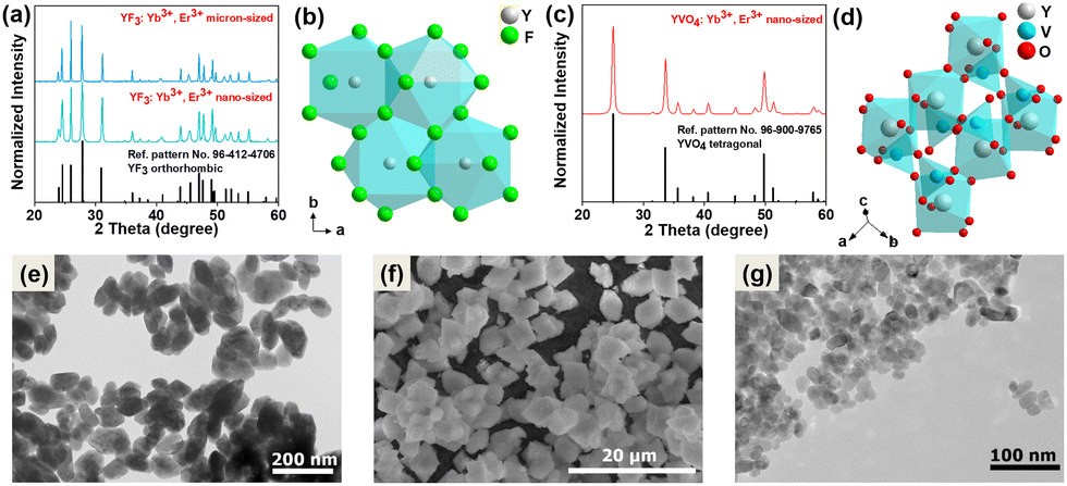 | ||
| Fig. 1 Powder XRD patterns of the (a) YF3:20% Yb3+, 2% Er3+ and (c) YVO4:20% Yb3+, 2% Er3+ and (b and d) corresponding graphical representation of the arrangement of atoms in the crystal lattice, TEM/SEM images of (e) nanocrystalline YF3:Yb3+, Er3+, (f) microcrystalline YF3:Yb3+, Er3+, and (g) nanocrystalline YVO4:Yb3+, Er3+. | ||
Luminescence properties
All synthesized samples exhibit intense green UCL clearly visible to the naked eye. Their emission spectra reveal narrow bands characteristic of Er3+ emission, namely the 2H11/2 → 4I15/2 (525 nm), 4S3/2 → 4I15/2 (550 nm) and 4F9/2 → 4I15/2 (660 nm) transitions, associated with 4f11–4f11 radiative transitions of Er3+ ions (see Fig. 2–4).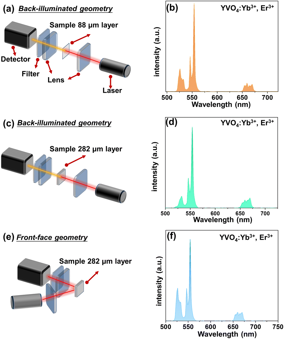 | ||
| Fig. 2 (a, c and e) Schematic representation of the experimental setup, i.e. optical geometry for the UCL measurements and (b, d and f) the corresponding UC emission spectra for the YVO4:Yb3+, Er3+ sample. (a–d) back-illuminated excitation geometry for the 88 μm thick sample (a and b), and for the 282 μm thick sample (c and d); (e and f) front-face excitation geometry for the 282 μm thick sample. | ||
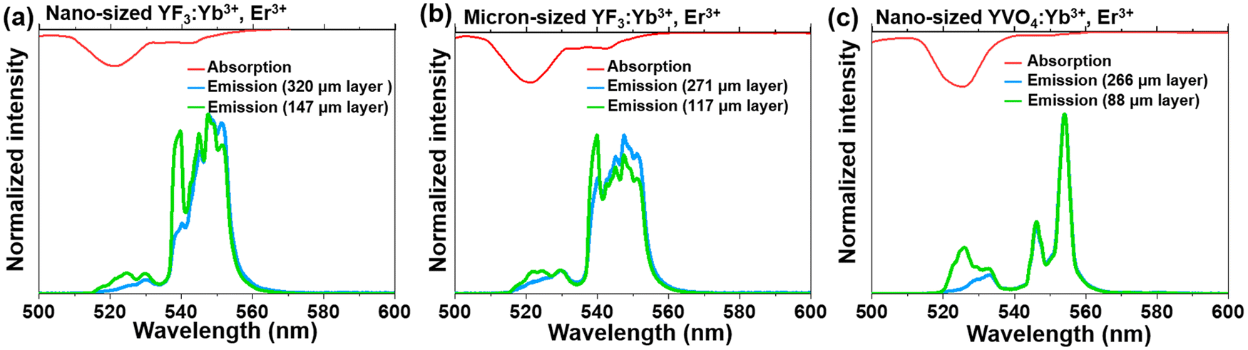 | ||
| Fig. 3 Normalized UC emission spectra of (a) the nano-sized YVO4:Yb3+, Er3+, (b) micron-sized YF3:Yb3+, Er3+, and (c) nano-sized YF3:Yb3+, Er3+, recorded for different sample thicknesses; (λex= 975 nm, bottom) combined with absorption spectra (top) of the obtained products. | ||
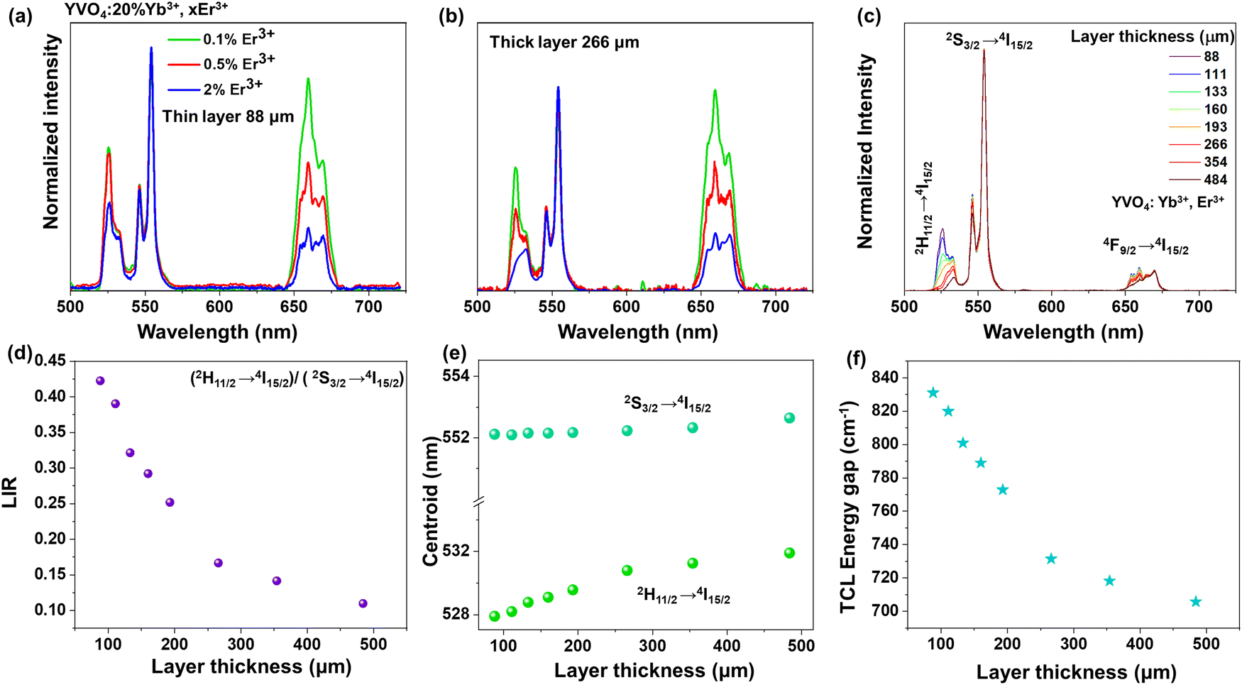 | ||
| Fig. 4 (a and b) Emission spectra of nanocrystalline YVO4:Yb3+, Er3+ recorded for different concentrations of Er3+ (0.1%, 0.5% and 2%) and for different sample thicknesses: (a) 88 μm and (b) 266 μm (c) emission spectra recorded for different layer thicknesses and corresponding (d) luminescence intensity ratios, (e) centroid associated with its 4f12–4f12-related 4S3/2 → 4I15/2 and 2H11/2 → 4I15/2 transitions, and (f) energy gap of the TCLs; λex = 975 nm. | ||
In order to simply check the potential effect of excitation-detection geometry and sample thickness on the shape of the UCL spectra, we have measured the same representative sample (YVO4:Yb3+, Er3+) with different thicknesses in back-illuminated (transmission) and front-face geometry, as depicted in Fig. 2. It is clear, that the emission spectrum of the thin-layer sample measured in the transmission geometry has a similar shape to the spectrum recorded in front-face geometry. However, in the case of UCL spectrum of the thick-layer sample measured in the transmission geometry, the 2H11/2 → 4I15/2-based emission band of Er3+ located around 525 nm has a much lower intensity, most plausibly due to partial reabsorption of the emitted light in this range. Additionally, we measured the UCL intensities vs. laser power and plotted them in a log–log representation and confirmed the square dependence of the non-linear UCL process (see Fig. S3, ESI†) on the incident laser power density.
In order to confirm the previously mentioned hypothesis and investigate in detail the anticipated reabsorption effects, we have measured the UC emission spectra for the synthesized micron- and nano-sized fluoride and vanadate materials (Fig. 3; bottom; λex = 975 nm), and compared them with absorption characteristics of these compounds (Fig. 3; top). The upper part of Fig. 3 shows the absorption spectra of the corresponding samples, presented in the 500–600 nm range (absorption spectra in the broader range, i.e. 200–1800 nm are shown in Fig. S4, ESI†). It can be seen that the absorption bands generally overlap with the emission bands, although a slight Stokes shift can be observed. It has already been elucidated by Hellwege and later by Ellens et al.49–51 that the electron–phonon coupling of 4fN levels (N = 1…13) is stronger for trivalent lanthanides close to an empty 4f0 (Ce3+, Pr3+, Nd3+) or fully filled 4f14 (Er3+ Tm3+, Yb3+) subshell, while those close to the half-filled 4f7 subshell (Eu3+, Gd3+, Tb3+) show the narrowest 4fn–4fn transitions among all lanthanide ions. Consequently, one would expect the largest emission bandwidths and Stokes shifts, and hence, re-absorption effects for the previously mentioned lanthanide ions including Er3+. It can be observed that for both materials (fluorides and vanadates) radiation in the 515–530 nm range is particularly strongly absorbed. In addition, in the case of fluorides, substantial absorption of radiation also occurs in the 645–660 nm range.
We were interested in the effect of sample thickness on the luminescence properties of the material, particularly how these factors affect the TCLs of Er3+ (2H11/2 and 4S3/2), which are related to the emission bands centered around 525 and 550 nm. For this purpose, the UC emission spectra of the samples with different layer thicknesses were measured in the back-illuminated geometry, and shown in the mentioned spectral range of interest, i.e. from 500 to 600 nm in Fig. 3. The spectral position of the emission band at 525 nm (2H11/2 → 4I15/2 transition) strongly overlaps with the respective absorption band with high oscillator strength (4I15/2 → 2H11/2 transition). This expectedly leads to re-absorption effects, dependent on the thickness of the sample layer. When the sample layer is very thin, the light reabsorption phenomenon occurs to a negligible extent, so the intensity of the 2H11/2 → 4I15/2 band is higher than for a thick-layer sample. In the case of a thicker sample layer, the phenomenon of selective reabsorption is more pronounced and results in a lowering of the respective band intensity. This is particularly noticeable for the vanadate material, which exhibits relatively strong absorption around 525 nm compared to the fluoride samples. In general, stronger absorption effects may be associated with enhanced defect-state absorption in the case of smaller NPs, typically containing more crystal defects. With the increase of the thickness of the sample layer, a more than 2-fold decrease in the intensity of the 525 nm band of Er3+ (located in the strongly absorbed region) was observed. At the same time, the band located around 550 nm (4S3/2 → 4I15/2 transition), where absorption of Er3+ is almost negligible, hardly changed its intensity. Non-normalized UC emission spectra recorded in the broader range, i.e. from 500 to 700 nm (see Fig. S5, ESI†) confirm the observed trend for the 4F9/2 → 4I15/2 band.
Due to the fact that modern optical thermometers are often based on changes in the relative intensities of the TCLs 2H11/2 and 4S3/2 of Er3+, and because of these changes were most pronounced for the YVO4 nanomaterial (comparing UCL spectra of the thin- and thick-layer samples), we decided to select this compound for further, more detailed studies. At first, to examine effect of Er3+ concentration on the shape and intensity of UCL spectra, three materials with varying Er3+ content (0.1, 0.5 and 2 mol%) were synthesized. As presented in Fig. 4a and b, with increasing amount of Er3+, the relative intensities (with respect to the emission at 550 nm, 4S3/2 → 4I15/2) of the emission peaks at 525 nm (2H11/2 → 4I15/2) and 660 nm (4F9/2 → 4I15/2) significantly decreased. Importantly, the intensity of the 2H11/2 → 4I15/2-based emission at 525 nm decreased much more for the thick-layer sample (Fig. 4b), confirming the discussed reabsorption phenomenon, resulting in a decrease in the intensity of the 2H11/2 → 4I15/2 band with respect to the intensity of the 4S3/2 → 4I15/2-related emission band. It should be noted that a significant decrease of the relative intensity of the red emission at 660 nm may also be related to cross-relaxation processes, which are typically enhanced in highly doped materials.52–54 Non-normalized emission spectra with increasing doping amount of Er3+ are included in the ESI† data (Fig. S6).
In the next step, the UC emission spectra of the nano-sized YVO4:20% Yb3+, 2% Er3+ samples were recorded in the range of 500–725 nm in back-illuminated excitation geometry for 8 samples with different thicknesses of the material layer (ranging from 88 to 484 μm; Fig. 4c). It was done in order to analyze spectroscopic parameters such as luminescence intensity ratio (LIR), position of the band centroids and size of the energy gap between the TCLs (Fig. 4d–f). It is observable that with increasing sample thickness the intensity of the 525 nm band gradually decreases compared to the 550 nm band. The emission at 660 nm also decreases to a smaller extent compared to the one at 525 nm. Subsequently, the LIR for the TCLs of the Er3+ ions (2H11/2 → 4I15/2/4S3/2 → 4I15/2), i.e. the intensity ratio of the integrated 525/550 nm emission bands was determined and plotted as a function of the sample thickness in Fig. 4d. With increasing thickness of the sample, the LIR values gradually decrease, which can be assigned to a higher reabsorption of light emitted from the excited 2H11/2 state in the thicker materials.
Due to the decrease in the intensity of the 525 nm band (2H11/2 → 4I15/2) with increasing thickness of the sample layer, its centroid shifts into higher wavelengths, while the centroid of the non-absorbed 550 nm band (4S3/2 → 4I15/2) remains constant, as shown in Fig. 4e. As a consequence, the energy gap value between the TCLs, derived from the spectra, decreases by around ≈ 115 cm−1 (from ≈ 831 cm−1 to 708 cm−1) with increasing thickness of the sample layer, as presented in Fig. 4f.
An alternative explanation for the observation of a decreasing LIR with increasing sample thickness could be ineffective heat transfer along the sample, which may result in changes of the thermalization between the 2H11/2 and 4S3/2 levels of Er3+, respectively. It should be noted that prior to any luminescence measurements, the laser power was set sufficiently low to avoid an uncontrolled increase in the local temperature of the samples, which could be potentially caused by the light-to-heat conversion effect. This could be especially relevant for thin sample layers, which in general are more susceptible to optical heating with the laser beam. Such laser-induced sample heating effect manifests in a form of thermalization of states of Er3+ TCLs, leading to the increasing of LIR values as a function of laser power, measured under ambient conditions. In order to exclude this possibility, the UC emission spectra of the obtained compounds were measured at different incident excitation power densities and the impact on the corresponding LIR values for the TCLs of the Er3+ ions (2H11/2 → 4I15/2/4S3/2 → 4I15/2) was investigated (see Fig. S7, ESI†). It is evident that for both samples (vanadate with different sample thicknesses) the LIR values of the Er3+ TCL bands remain constant up to ≈ 11 W cm−2 revealing that the laser-induced heating effect is negligible in the low-power density range used during the measurements and starts to be detectable around ≈ 15 W cm−2.
Changes in the values of the previously mentioned spectroscopic parameters induced by the reabsorption phenomena can be relevant in the development of optical, remote nanothermometers. In order to check how the thickness of the sample layer affects the thermometric properties and performance of luminescence thermometers, the UC emission spectra of the thin- and thick-layer vanadate nanomaterial were measured as a function of temperature, in the range of 298–573 K (Fig. 5a and e; λex = 975 nm) in transmission geometry. In both cases the intensity of the 4S3/2 → 4I15/2-based emission decreases in favor of the intensity of the 2H11/2 → 4I15/2-based emission with increasing temperature. The thermal equilibrium between those two excited levels of Er3+ follows Boltzmann's law:
 | (1) |
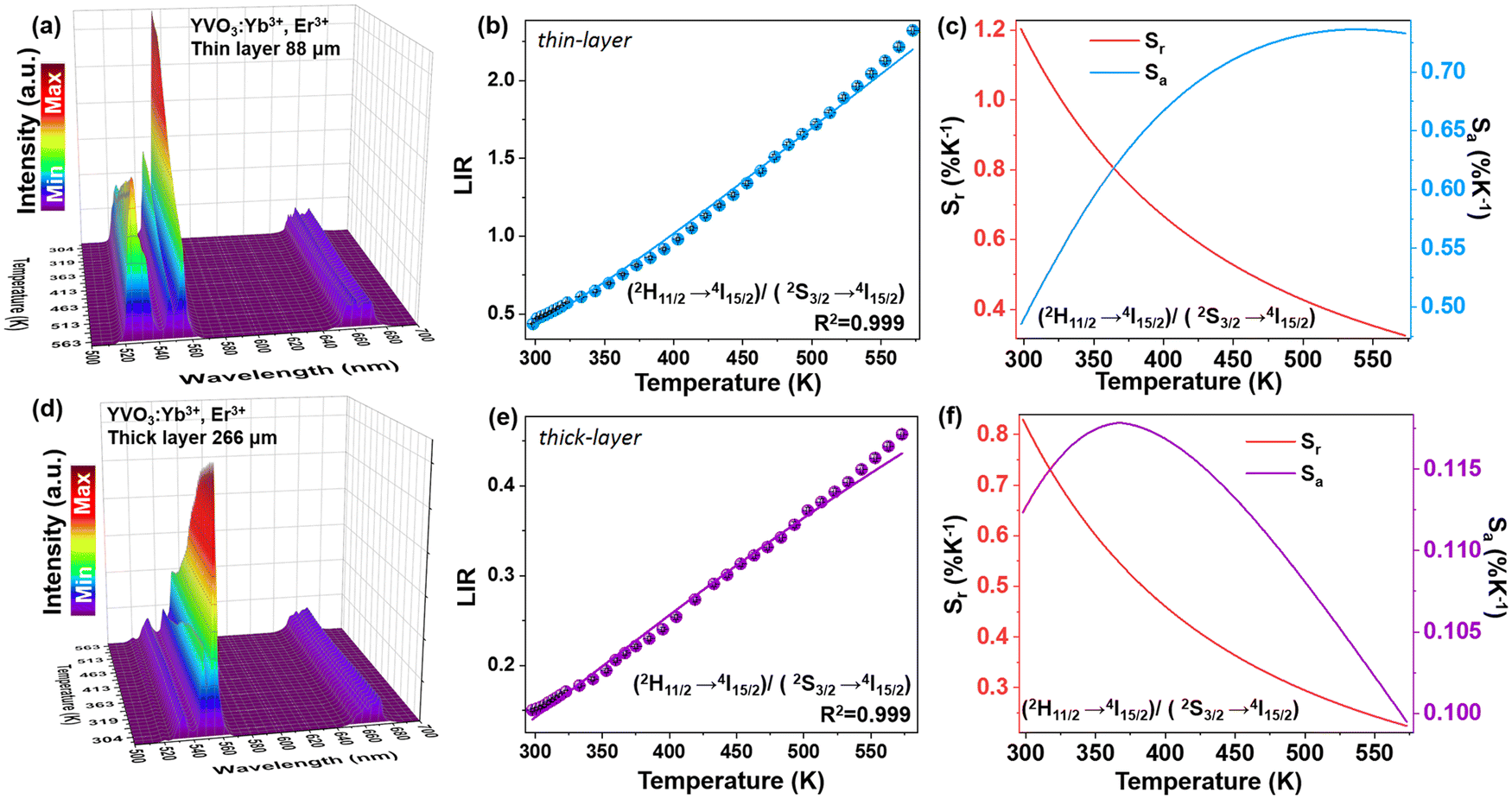 | ||
| Fig. 5 (a and d) UC emission spectra of the thin-layer (a) and thick-layer (d) sample of YVO4:Er3+, Yb3+ nanocrystals measured at increasing temperature values (λex = 975 nm); (b and e) the determined LIR values (525/550 nm) and (c and f) the corresponding Sr and Sa values as a function of temperature, obtained for the thin-layer (b and c) and thick-layer (e and f) samples, respectively. | ||
In order to investigate the performance of any nanothermometer, parameters such as absolute sensitivity and relative sensitivities should be determined.9 The absolute sensitivity (Sa) was calculated based on the eqn (2). This parameter is usually expressed in K−1.45
 | (2) |
However, the relative temperature sensitivity, Sr, allows to quantitatively compare thermometers with different operating principles (developed using different measuring setups). This parameter reflects by what amount the analyzed thermometric parameter (LIR) changes per 1 K (typically expressed in % K−1),45 and it is defined according to the eqn (3).
 | (3) |
Importantly, the thin-layer sample (thickness of 88 μm) has maximum Sr value of 1.2% K−1 at 298 K and Sa of 0.73% K−1 (Fig. 5c), while the thick-layer sample (thickness of 266 μm) has much lower maximum Sr value, reaching only ≈0.85% K−1 at 298 K and Sa of 0.12% K−1 (Fig. 5f). However, please note that the Sr parameter is a statistical error measure (it is not a systematic error), and reabsorption gives rise to a systematic error that needs to be taken into account to get the actual correct temperature.
Due to the strong temperature dependence of the determined thermometric parameters and derived quantities, i.e. LIR and Sr, there is a necessity for recalibration of the developed thermometers, always when they are used in different conditions and/or in a different form. Moreover, it is clear that depending on the measuring conditions, the increase in the sample thickness may deteriorate performance of luminescent thermometers.
Conclusions
In this work, the influence of the sample layer thickness and excitation geometry on the luminescence properties of the material was investigated. Using exemplary fluoride and vanadate materials activated with Er3+ ions, it has been shown that in the case of the back-illuminated excitation geometry, the effect of reabsorption on the luminescence properties of the material is more pronounced with the increase in the thickness of the sample layer. This phenomenon causes an artificial lowering of the LIR (by a factor of almost 5) and thus, a severe systematic bias in temperature measurements with the thermally coupled excited 2H11/2 and 4S3/2 levels of Er3+ ions. A conclusion from this work is that the operating principle of primary thermometers is only valid and accurate for sufficiently thin sample layers, in which the observed reabsorption effects are marginal, or in the case of optical temperature measurements/readouts performed in a front-face detection geometry. Moreover, the results presented emphasize a significant impact of the experimental setup and reabsorption on the remote temperature readings and performance of optical temperature sensors, having severe implications for the community working in the area of luminescence thermometry.Author contributions
N. S.: data curation, formal analysis, funding acquisition, investigation, validation, writing – original draft, P. W.: formal analysis, investigation, M. S.: data curation, investigation, writing – review & editing, T. Z.: validation, visualization, S. L.: resources, supervision, writing – review & editing, M. R.: conceptualization, data curation, funding acquisition, investigation, project administration, supervision, writing – review & editing.Conflicts of interest
There are no conflicts to declare.Acknowledgements
This work was supported by the Polish National Science Centre (grant no. 2018/31/N/ST4/00684 and 2018/31/N/ST5/00636). M. S. is grateful for funding from a materials cost allowance of the Fonds der Chemischen Industrie e.V. and a scholarship from the “Junges Kolleg” of the North Rhine-Westphalian Academy of Sciences and Arts. M. R. acknowledges support from Fondo Social Europeo and Agencia Estatal de Investigación (RYC2020-028778-I/AEI/10.13039/501100011033).Notes and references
- M. Runowski, N. Stopikowska, D. Szeremeta, S. Goderski, M. Skwierczyńska and S. Lis, ACS Appl. Mater. Interfaces, 2019, 11, 13389–13396 CrossRef CAS PubMed.
- Z. Chen, H. Jia, K. Sharafudeen, W. Dai, Y. Liu, G. Dong and J. Qiu, J. Alloys Compd., 2016, 663, 204–210 CrossRef CAS.
- K. Nigoghossian, M. F. S. Peres, F. L. Primo, A. C. Tedesco, E. Pecoraro, Y. Messaddeq and S. J. L. Ribeiro, Colloids Interface Sci. Commun., 2014, 2, 6–10 CrossRef CAS.
- Q. Liu, W. Feng and F. Li, Coord. Chem. Rev., 2014, 273–274, 100–110 CrossRef CAS.
- M. K. Tsang, C. F. Chan, K. L. Wong and J. Hao, J. Lumin., 2015, 157, 172–178 CrossRef CAS.
- N. Stopikowska, M. Runowski, P. Woźny, S. Goderski and S. Lis, J. Lumin., 2020, 228, 117643 CrossRef CAS.
- M. Runowski, Pressure and temperature optical sensors: Luminescence of lanthanide-doped nanomaterials for contactless nanomanometry and nanothermometry, in Handbook of Nanomaterials in Analytical Chemistry, ed. C. M. Hussain, Elsevier, 2020, pp. 227–273 DOI:10.1016/B978-0-12-816699-4.00010-4.
- D. Jaque and F. Vetrone, Nanoscale, 2012, 4, 4301–4326 RSC.
- L. R. Dačanin, S. R. Lukić-Petrović, D. M. Petrović, M. G. Nikolić and M. D. Dramićanin, J. Lumin., 2014, 151, 82–87 CrossRef.
- C. D. S. Brites, A. Millán and L. D. Carlos, Handb. Phys. Chem. Rare Earths, 2016, 49, 339–427 CAS.
- R. Ma, R. Shimmon, A. McDonagh, P. Maynard, C. Lennard and C. Roux, Forensic Sci. Int., 2012, 217, 22–25 CrossRef PubMed.
- J. C. G. Bünzli, Trends Chem., 2019, 1, 751–762 CrossRef.
- M. Runowski, A. Shyichuk, A. Tymiński, T. Grzyb, V. Lavín and S. Lis, ACS Appl. Mater. Interfaces, 2018, 10, 17269–17279 CrossRef CAS PubMed.
- A. Nadort, J. Zhao and E. M. Goldys, Nanoscale, 2016, 8, 13099–13130 RSC.
- W. Zheng, P. Huang, D. Tu, E. Ma, H. Zhu and X. Chen, Chem. Soc. Rev., 2015, 44, 1379–1415 RSC.
- S. Goderski, M. Runowski, N. Stopikowska and S. Lis, J. Lumin., 2017, 188, 24–30 CrossRef CAS.
- F. Karely Chamé, M. Miguel Ojeda, G. Federico González, T. Víctor M. Rentería, M. Ma. Luisa Ojeda and O. Celso Velásquez, J. Alloys Compd., 2018, 744, 683–690 CrossRef.
- Y. Liu, D. Tu, H. Zhu and X. Chen, Chem. Soc. Rev., 2013, 42, 6924–6958 RSC.
- H. Suo, F. Hu, X. Zhao, Z. Zhang, T. Li, C. Duan, M. Yin and C. Guo, J. Mater. Chem. C, 2017, 5, 1501–1507 RSC.
- P. Qiu, N. Zhou, H. Chen, C. Zhang, G. Gao and D. Cui, Nanoscale, 2013, 5, 11512–11525 RSC.
- A. Gnach and A. Bednarkiewicz, Nano Today, 2012, 7, 54–66 CrossRef.
- D. Chen, Z. Wan, Y. Zhou, X. Zhou, Y. Yu, J. Zhong, M. Ding and Z. Ji, ACS Appl. Mater. Interfaces, 2015, 7, 19484–19493 CrossRef CAS PubMed.
- M. D. Dramićanin, J. Appl. Phys., 2020, 128, 040902 CrossRef.
- F. H. Borges, J. C. Martins, F. J. Caixeta, L. D. Carlos, R. A. S. Ferreira and R. R. Gonçalves, J. Lumin., 2022, 248, 118986 CrossRef CAS.
- H. Suo, X. Zhao, Z. Zhang, Y. Wang, J. Sun, M. Jin and C. Guo, Laser Photonics Rev., 2021, 15, 1–25 Search PubMed.
- M. Runowski, P. Wozny, N. Stopikowska, I. R. Martín, V. Lavín and S. Lis, ACS Appl. Mater. Interfaces, 2020, 12, 43933–43941 CrossRef CAS PubMed.
- G. Dantelle, V. Reita and C. Delacour, Nanomaterials, 2021, 11(2), 479 CrossRef CAS PubMed.
- C. D. S. Brites, E. D. Martínez, R. R. Urbano, C. Rettori and L. D. Carlos, Front. Chem., 2019, 7, 267 CrossRef CAS PubMed.
- A. M. P. Botas, C. D. S. Brites, J. Wu, U. Kortshagen, R. N. Pereira, L. D. Carlos and R. A. S. Ferreira, Part. Part. Syst. Charact., 2016, 33, 740–748 CrossRef CAS.
- W. Xu, H. Zhao, Y. Li, L. Zheng, Z. Zhang and W. Cao, Sens. Actuators, B, 2013, 188, 1096–1100 CrossRef CAS.
- W. Xu, Q. Song, L. Zheng, Z. Zhang and W. Cao, Opt. Lett., 2014, 39, 4635 CrossRef CAS PubMed.
- S. Balabhadra, M. L. Debasu, C. D. S. Brites, R. A. S. Ferreira and L. D. Carlos, J. Phys. Chem. C, 2017, 121, 13962–13968 CrossRef CAS.
- A. A. Kalinichev, M. A. Kurochkin, E. V. Golyeva, A. V. Kurochkin, E. Lähderanta, M. D. Mikhailov and I. E. Kolesnikov, J. Lumin., 2018, 195, 61–66 CrossRef CAS.
- C. D. S. Brites, P. P. Lima, N. J. O. Silva, A. Millán, V. S. Amaral, F. Palacio and L. D. Carlos, Nanoscale, 2012, 4, 4799–4829 RSC.
- T. Bai and N. Gu, Small, 2016, 12, 4590–4610 CrossRef CAS PubMed.
- S. Mahlik, M. Grinberg, E. Cavalli, M. Bettinelli and P. Boutinaud, J. Phys.: Condens. Matter, 2009, 21, 105401 CrossRef CAS PubMed.
- I. K. van Ravenhorst, R. G. Geitenbeek, M. J. van der Eerden, J. Tijn van Omme, H. H. Peréz Garza, F. Meirer, A. Meijerink and B. M. Weckhuysen, ChemCatChem, 2019, 11, 5505–5512 CrossRef CAS.
- P. Woźny, M. Runowski and S. Lis, J. Lumin., 2019, 209, 321–327 CrossRef.
- M. Runowski, P. Woźny, N. Stopikowska, Q. Guo and S. Lis, ACS Appl. Mater. Interfaces, 2019, 11, 4131–4138 CrossRef CAS PubMed.
- T. Zheng, M. Runowski, N. Stopikowska, M. Skwierczyńska, S. Lis, P. Du and L. Luo, J. Alloys Compd., 2021, 890, 161830 CrossRef.
- M. A. Hernández-Rodríguez, A. D. Lozano-Gorrín, I. R. Martín, U. R. Rodríguez-Mendoza and V. Lavín, Sens. Actuators, B, 2018, 255, 970–976 CrossRef.
- F. H. Borges, J. C. Martins, F. J. Caixeta, R. R. Pereira, L. D. Carlos, R. A. S. Ferreira and R. R. Gonçalves, J. Sol-Gel Sci. Technol., 2022, 102, 249–263 CrossRef CAS.
- Y. Gao, F. Huang, H. Lin, J. Xu and Y. Wang, Sens. Actuators, B, 2017, 243, 137–143 CrossRef CAS.
- J. C. Martins, A. R. N. Bastos, R. A. S. Ferreira, X. Wang, G. Chen and L. D. Carlos, Adv. Photonics Res., 2021, 2, 2000169 CrossRef CAS.
- N. Stopikowska, M. Runowski, M. Skwierczyńska and S. Lis, Nanoscale, 2021, 13, 14139–14146 RSC.
- C. D. S. Brites, S. Balabhadra and L. D. Carlos, Adv. Opt. Mater., 2019, 7, 1–30 Search PubMed.
- A. Bednarkiewicz, L. Marciniak, L. D. Carlos and D. Jaque, Nanoscale, 2020, 12, 14405–14421 RSC.
- A. Nexha, M. C. Pujol, F. Díaz, M. Aguiló and J. J. Carvajal, Opt. Mater., 2022, 134, 113216 CrossRef CAS.
- A. M. G. B. A. Ellens and H. Andres, Phys. Rev. B: Condens. Matter Mater. Phys., 1997, 55, 173–179 CrossRef CAS.
- G. B. A. Ellens, H. Andres, M. L. H. ter Heerdt, R. T. Wegh and A. Meijerink, Phys. Rev. B: Condens. Matter Mater. Phys., 1997, 55, 529–542 Search PubMed.
- K. H. Hellwege, Ann. Phys., 1941, 432, 529–542 CrossRef.
- H. Wang, M. Xing, X. Luo, X. Zhou, Y. Fu, T. Jiang, Y. Peng, Y. Ma and X. Duan, J. Alloys Compd., 2014, 587, 344–348 CrossRef CAS.
- D. Pugliese, N. G. Boetti, J. Lousteau, E. Ceci-Ginistrelli, E. Bertone, F. Geobaldo and D. Milanese, J. Alloys Compd., 2016, 657, 678–683 CrossRef CAS.
- S. Ryszczyńska, K. Trejgis, Ł. Marciniak and T. Grzyb, ACS Appl. Nano Mater., 2021, 4, 10438–10448 CrossRef.
- T. P. van Swieten, T. van Omme, D. J. van den Heuvel, S. J. W. Vonk, R. G. Spruit, F. Meirer, H. H. P. Garza, B. M. Weckhuysen, A. Meijerink, F. T. Rabouw and R. G. Geitenbeek, ACS Appl. Nano Mater., 2021, 4(4), 4208–4215 CrossRef CAS PubMed.
- P. Rühl, D. Wang, F. Garwe, R. Müller, M. Haase, K. W. Krämer, W. Pa, R. Heintzmann, S. H. Heinemann and H. Stafast, J. Lumin., 2021, 232, 117860 CrossRef.
Footnote |
| † Electronic supplementary information (ESI) available. See DOI: https://doi.org/10.1039/d3tc01684f |
| This journal is © The Royal Society of Chemistry 2023 |