
 Open Access Article
 This Open Access Article is licensed under a
 Creative Commons Attribution 3.0 Unported Licence
Crystalline solid retains memory of anisotropy in precursor liquid crystalline phase†
Kushal
Bagchi
 a,
Tadej
Emeršič
a,
Zhongyang
Wang
a,
Wen
Chen
a,
Mincheol
Kim
a,
Christopher
Eom
a,
Zhang
Jiang
b,
Joseph
Strzalka
b,
Juan J.
de Pablo
ac and
Paul F.
Nealey
*ac
a,
Tadej
Emeršič
a,
Zhongyang
Wang
a,
Wen
Chen
a,
Mincheol
Kim
a,
Christopher
Eom
a,
Zhang
Jiang
b,
Joseph
Strzalka
b,
Juan J.
de Pablo
ac and
Paul F.
Nealey
*ac
aPritzker School of Molecular Engineering, The University of Chicago, Chicago, Illinois 60637, USA. E-mail: nealey@uchicago.edu
bX-ray Science Division, Argonne National Laboratory, Lemont, Illinois 60439, USA
cMaterials Science Division, Argonne National Laboratory, Lemont, Illinois 60439, USA
First published on 31st July 2023
Abstract
From chemical reactivity to mechanical strength, crystal texture plays a central role in determining the key properties of solids. In organic electronics, texture determines the charge carrier mobility of the active layer in devices such as organic field effect transistors (OFETs). Current methods of controlling the texture of thin films of organic crystals through solution processing are restricted by the stochastic nucleation that accompanies rapid solvent evaporation. We report here a facile method to create biaxially textured crystals of thin films of discotic organic semiconductor, HAT6 (2,3,6,7,10,11-Hexakis(hexyloxy)triphenylene). We first direct the self-assembly of the precursor discotic liquid crystalline (DLC) state; the columnar hexagonal (ColH) phase of HAT6 is biaxially aligned in lithographically fabricated microchannels. Synchrotron X-ray scattering measurements reveal the direction of π-stacking is perpendicular to the channel walls. The biaxial alignment and the directionality of π-stacking in the liquid crystalline phase are transferred to the crystalline state through rapid cooling. Contrary to previous reports, we observe preservation of anisotropy upon crystallization of DLCs. As a significant fraction of organic semiconductors exhibit a liquid crystalline phase, we expect our method of creating textured crystals to be of broad interest.
Introduction
From structural biology to material science, understanding structure at the molecular level is intimately linked with our ability to grow single crystals. Single crystals enable investigation of the intrinsic properties of materials and are necessary for fundamental understanding of transport in solids. Identification of new strategies to grow large single crystals can have far-reaching technological implications. The Czochralski method of growing single crystalline inorganic semiconductors has made modern integrated circuits possible. An analogous ability to control the molecular organization of organic materials over macroscopic length scales is therefore expected to have far-reaching technological implications, especially for fields such as organic electronics and photonics.1,2 For instance, the performance of organic field effect transistors (OFETs) is highly dependent on the degree of lattice orientation or “the texture” of organic crystals in thin films.3The inherent complexity of organic molecules can complicate the growth of large single crystals. The challenge of forming single crystals of organic molecules is further exacerbated for thin films which are formed by processes far from equilibrium such as physical vapor deposition and spin-coating. Growing highly textured, single crystalline molecular solids in confined geometries such as thin films is a fundamental problem in crystal nucleation and growth, the resolution of which is likely to have far-reaching implications for organic electronics.
Thin films of organic semiconductors are generally prepared either by vacuum deposition or solution processing. While vacuum deposition offers several advantages for growth of organic thin films it is an expensive method and suited for high-end applications. As solution processing is more viable for low-cost and large-area coating applications than vacuum deposition, a variety of solvent-based techniques have been used to deposit thin, crystalline films of small molecule organic semiconductors. Several approaches have been used to optimize crystal texture of solution-processed films such as dip-coating,4 zone casting,5 solution shearing,6 and fluid-enhanced crystal engineering7 (FLUENCE). However, the stochastic nature of nucleation that results from rapid solvent evaporation hinders the formation of single crystals for most of these approaches. Crystallization from a rapidly evaporating solvent can also result in other undesirable outcomes such as dendritic growth and thickness non-uniformity. The techniques that have been used to form single crystalline states directly from solution typically involve controlling several process parameters simultaneously. A facile and scalable method of producing biaxial crystals of organic semiconductors in the thin film format is lacking and would have broad implications both for organic electronics and for fundamental understanding of transport in molecular solids.
We demonstrate here that liquid crystallinity can be harnessed to prepare biaxial crystals of organic semiconductors. We use lithographically fabricated microchannels to attain biaxial alignment of thin films of discotic liquid crystal (DLC) former, HAT6. We demonstrate transfer of biaxiality from the discotic to crystalline phase, thereby challenging the view in the literature that crystallization of liquid crystals results in loss or reduction of anisotropy.8–11 We characterize the aligned phases using synchrotron grazing incidence wide-angle X-ray scattering (GIWAXS) as well as atomic force microscopy (AFM) and polarized optical microscopy (POM). In addition to triphenylenes, several other important organic semiconductors classes12–14 such as perylene diimides,15,16 porphyrins,17 phthalocyanines,18 and hexabenzocoronenes19,20 also exhibit discotic liquid crystalline phases, making our results of broad interest. We expect our method of attaining aligned molecular crystals will be of interest for applications that use discotic molecules such as organic transistors,5 light-emitting diodes,16 and solar cells.21
Results
HAT6 (2,3,6,7,10,11-Hexakis(hexyloxy)triphenylene) is a model DLC former and organic semiconductor. Shown in Fig. 1(a) is the chemical structure of HAT6. It has a conjugated, charge-conducting triphenylene core and six alkyl side chains that increase the molecule's solubility in organic solvents. Differential scanning calorimetry is performed to determine the phase transition temperatures of HAT6 (Fig. 1(b)). Consistent with previous reports,22 we observe two transitions at ≈100 °C and ≈65 °C, corresponding to the melting of the columnar hexagonal (ColH) and plastic crystalline phases into the isotropic and ColH phases, respectively. As shown in Fig. 1(c), in the ColH liquid crystalline state, HAT6 molecules self-assemble into columns which in turn organize hexagonally. The columnar structure is preserved in the plastic crystalline state of alkylated triphenylenes; however, the hexagonal symmetry is lost, and the cores are tilted with respect to the columnar axes.23 Shown in Fig. 1(d) is a schematic of the generic crystal structure that alkylated triphenylenes adopt. The organization of the triphenylene cores into columns in both the crystalline and liquid crystalline phases enables these materials to function as one-dimensional conductors or molecular wires. However, to harness one-dimensional charge conduction the columnar axis needs to be organized along the desired direction of transport.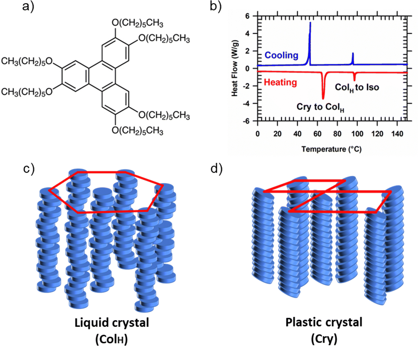 | ||
| Fig. 1 Structure and phase behavior of HAT6. (a) Chemical structure of HAT6. (b) Differential scanning calorimetry of HAT6. The columnar hexagonal phase (ColH) occurs between 65 to 100 °C. At room temperature, HAT6 is a plastic crystal. (c) Schematic representation of molecular packing in the liquid crystalline and (d) plastic crystalline phases. Only the triphenylene cores are depicted in the illustrations to emphasize the parts of the molecule that can exhibit ordering. | ||
Microchannels are known to induce directional planar alignment in DLCs.18 Structure in thin films of DLCs is determined by competition between the different molecular orientations that are favored at the air and solid interfaces. While molecules prefer to exhibit edge-on orientation at the free surface, face-on packing is favored at the buried solid interface. Introduction of two solid surfaces, perpendicular to the substrate makes directional planar alignment energetically favorable. Although the molecules adopt face-on packing with respect to the surfaces of the walls, with reference to the substrate the orientation is edge-on. Consequently, an overall planar alignment, with the direction of π-stacking perpendicular to the grating walls, results in energetically favorable molecular orientation at three out of four interfaces. The only unfavorable structure occurs at the horizontal substrate interface.
To induce planar alignment of the ColH phase, microchannels are fabricated using photolithography. The workflow for the preparation of microchannels with cross-linked polystyrene (X-PS) walls on a silicon substrate is shown in Fig. 2(a). X-PS is spin-coated onto a silicon wafer; cross-linking is induced by thermal annealing. Photolithography is performed to create alternating regions of exposed and photoresist-protected polystyrene. The exposed regions are etched away using oxygen plasma and the photoresist is subsequently stripped in solvent resulting in microchannels on silicon with X-PS walls. An AFM image of the topographical pattern before filling with HAT6 is shown in Fig. 2(b). The bright and dark regions are the polystyrene and silicon regions, respectively. The pattern pitch and channel width are ≈5 and 3 μm, respectively; this pattern geometry is utilized in all the POM images shown subsequently (in the main manuscript). HAT6 is spin-coated onto the patterns, heated to the isotropic phase, and cooled to the discotic phase to induce alignment. The film is then cooled to room temperature for imaging under the POM. The AFM image of the patterned region after spin-coating and thermal processing is shown in Fig. 2(c). Linecuts of the AFM images in Fig. 2 are shown in Fig. S1 (ESI†). The AFM image and the linecut (Fig. S1, ESI†) indicate that HAT6 partially fills the trenches and grows selectively on the silicon regions.
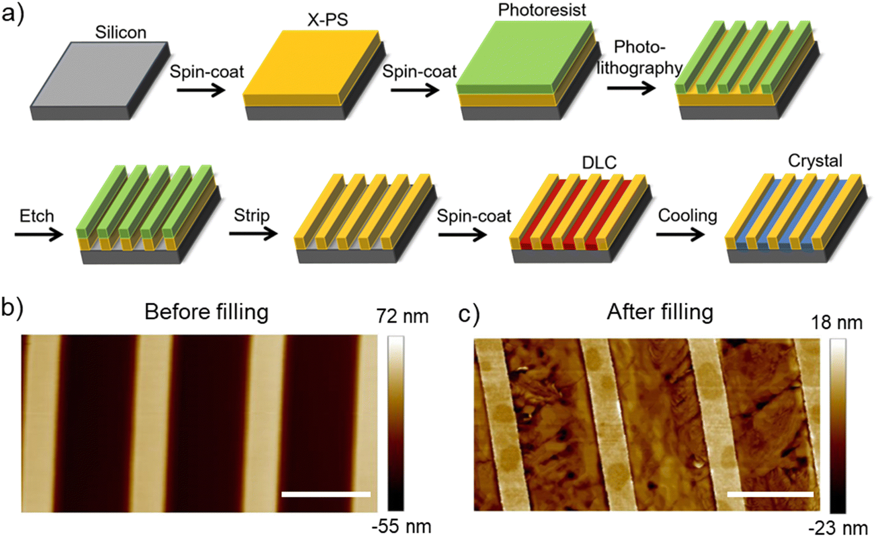 | ||
| Fig. 2 Fabrication and characterization of microchannels for alignment of HAT6. (a) Schematic representation of the fabrication process to prepare microchannels with cross-linked polystyrene (X-PS) walls on a silicon substrate. AFM images of channels (b) before and (c) after filling with HAT6. The thickness of the spin-coated HAT6 film is ≈70 nm. The scale bar for AFM images is 4 μm. HAT6 partially fills the trenches, growing preferentially on the silicon regions. | ||
The plastic crystal state of HAT6, obtained from cooling the liquid crystalline phase exhibits biaxial alignment. Shown in Fig. 3 are POM images, taken at room temperature, for films of HAT6 spin-coated onto ≈3 μm wide polystyrene channels. The thinnest film is ≈30 nm while the thickest film is ≈130 nm. The square region in the images is the patterned region while the area outside it is the un-patterned background. Images are taken with the channel walls along and rotated 45° with respect to the crossed polarizers. Characteristic of directional planar alignment, the intensity under a crossed polarized geometry changes with rotating the sample in-plane. A video of the change of intensity with in-plane rotation can be found in Supplemental Video S1 (ESI†).
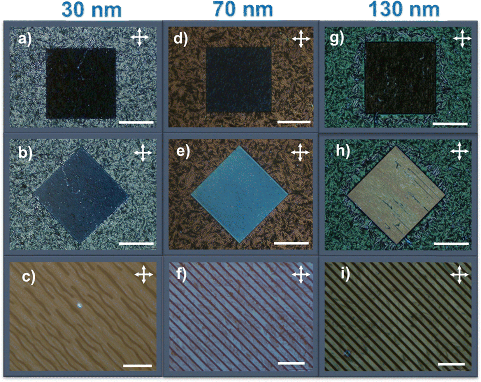 | ||
| Fig. 3 Alignment of plastic crystalline phase of HAT6 in microchannels. POM images of crystalline HAT6 films of thickness 30 nm (a)–(c), 70 nm (d)–(f), and 130 nm (g)–(i). All images were acquired at room temperature where HAT6 is a crystal. POM images are taken at 4× magnification at 0° (a), (d), and (g) and 45° (b), (e), and (h) angles of the channel walls with respect to the crossed polarizers. Images are also taken at a 100× magnification and 45° rotation (c), (f), and (i). Scale bar for (a), (b), (d), (e), (g), and (h) is 500 μm and (c), (f), and (i) is 20 μm. Alignment of the HAT6 crystals is possible down to ≈30 nm. The X-PS grating heights are 35 nm, 80 nm, and 180 nm for (a)–(c), (d)–(f), and (g)–(i), respectively. | ||
The degree of biaxial alignment of HAT6 crystals in microchannels is quantitatively similar in the thickness range of interest for organic electronic applications. For quantitative analysis, the POM images shown in Fig. 3 are integrated. The difference in the average intensity in the patterned regions at 0° and 45° is a measure of biaxial alignment. The sum of intensities at 0° and 45° is used as a normalization factor. The variable plotted in the Y-Axis in Fig. 4, 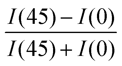 is 1 when there is perfect biaxial alignment; the quantity is zero when the structure is random in-plane. The quantitative analysis, shown in Fig. 4 indicates that films in the range of 30–130 nm show a quantitatively similar degree of alignment in the microchannels. De-wetting prevents exploration of films thinner than 30 nm (Fig. 3(c)). The 70 nm film however exhibits a smooth and continuous morphology in the microchannels, as is evident from the AFM image in Fig. 2 and POM images in Fig. 3. In addition to thickness uniformity, the smooth textures observed in Fig. 3(e), (f), (h) and (i) arise from the absence of grain boundaries. The POM images of a HAT6 film deposited on un-patterned silicon and subjected to the same thermal treatment are shown in Fig. S2 (ESI†) for comparison. On un-patterned silicon, HAT6 thin films exhibit a granular and polycrystalline morphology.
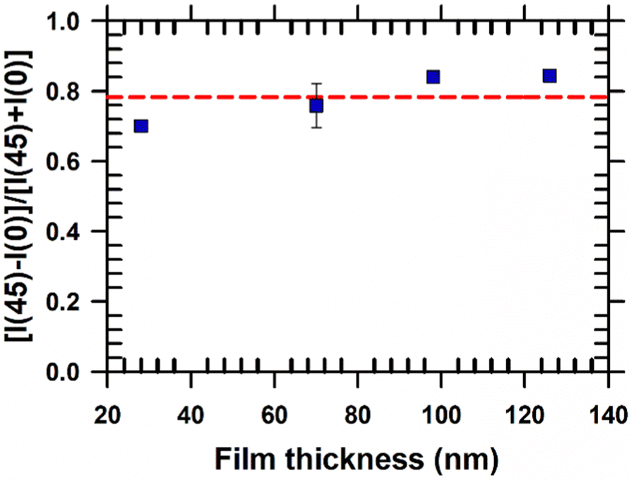 | ||
| Fig. 4 Quantification of biaxial alignment of crystalline HAT6 films in microchannels. The POM images shown in Fig. 3 are integrated to quantify the difference in intensity between images collected when the channel is at 45° and 0° with respect to the crossed polarizers. The pitch and width of the channels are ≈5 μm and ≈3 μm respectively, for all samples analyzed. The red-dotted line is an eye guide. Alignment of HAT6 crystals is quantitatively similar for films that are 30 to 130 nm in thickness. | ||
Our results indicate that up to a film thickness of ≈30 nm, structure is determined by interactions of HAT6 molecules with the side walls and at the free surface. It is conceivable that below a certain critical thickness the structure will be determined by the substrate and the molecular orientation will flip from edge-on to face-on. Future studies using narrower channels, which will more efficiently inhibit de-wetting and allow exploration of packing in even thinner films, could shed light on whether there is a thickness limit for grapho-epitaxial alignment. A bottleneck for the use of liquid crystal films for sub 5 nm lithography24 is attaining alignment in ultrathin films. An essential step in using soft materials for lithography is pattern transfer; for pattern transfer of small features sizes alignment is required in ultrathin films.
Biaxial alignment of HAT6 crystals in microchannels is possible even when the chemical nature of the confining surface is vastly different. The lithographic workflow shown in Fig. 2 was modified to create channels where the walls are also made of silicon or gold. As shown in Fig. S3 and Table S1 (ESI†), quantitatively similar results are obtained when the channel walls are composed of silicon, gold, and polystyrene. Similarly, alignment is quantitatively alike when the bottom surface is modified through silanization. Our results suggest that geometry rather than chemistry determines the optical texture of thin films of discotic molecules.
To probe structure at molecular length scales we perform X-ray scattering. Specifically, we perform synchrotron grazing incidence wide-angle X-ray scattering (GIWAXS), a technique well-suited to study the structure of organic thin films.25 For GIWAXS measurements, the pattern geometry is altered to decrease the fraction of polystyrene; the channel width and pitch are increased to ≈8 and 10 μm, respectively. Polystyrene produces an amorphous halo in reciprocal space close to the π-stacking peaks of interest. POM images of aligned HAT6 crystals in this pattern geometry are shown in Fig. S4 (ESI†); biaxially aligned crystals are formed in wider channels as well. Shown in Fig. 5 are GIWAXS patterns from HAT6 deposited on patterned and un-patterned substrates. Qz and Qy represent scattering vectors in the out-of-plane and in-plane directions, respectively. Qz is along the surface normal, while Qy is perpendicular both to Qz and the incoming X-ray beam. The color in the two-dimensional scattering patterns represents intensity. Red and blue represent high and low scattered intensity, respectively. The samples are processed as described earlier.
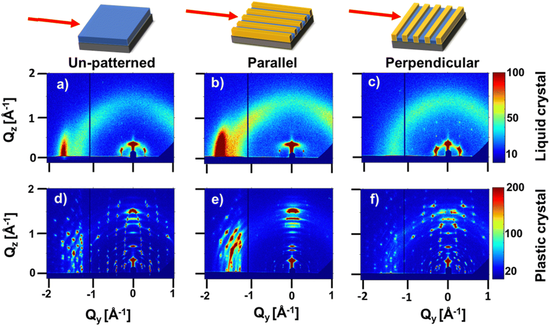 | ||
| Fig. 5 X-ray scattering patterns from HAT6 thin films in liquid crystal and plastic crystal states on un-patterned and patterned substrates. GIWAXS (grazing incidence wide-angle X-ray scattering) patterns collected in the liquid crystal state (80 °C) on (a) an un-patterned substrate and on a patterned substrate with channel walls (b) parallel and (c) perpendicular to the X-ray beam. GIWAXS patterns in the crystalline state (25 °C) on (d) an un-patterned substrate and on a patterned substrate with channel walls (e) parallel and (f) perpendicular to the X-ray beam. The film thicknesses are between 50–60 nm. For b, c, e, and f, the width of the channels and pitch of the patterns are ≈8 μm and ≈10 μm, respectively. The biaxial anisotropy of the liquid crystalline state is transferred to the crystalline state. The gratings and the films are of approximately the same thickness. | ||
In the liquid crystalline phase of HAT6, molecules exhibit edge-on packing on the un-patterned silicon substrate. Two peaks are visible in Fig. 5(a). At Qy ≈ 1.7 Å−1 and d ≈ 3.7 Å is the peak that corresponds to π-stacking. The excess scattered intensity along Qy, as compared to Qz, is indicative of edge-on packing. The peak at Q ≈ 0.35 Å−1 corresponds to the spacing between the centers of the columns. The presence of both columnar peaks (spacing between columns) and π-stacking peaks in the same pattern indicates the structure, in the sample deposited on silicon, is random in-plane.
When the DLC phase is random in-plane, the plastic crystalline state exhibits uniaxial texture. Shown in Fig. 5(d) is the X-ray scattering pattern from a HAT6 thin film on un-patterned silicon, collected at room temperature where it is a crystal. Consistent with expectations, the pattern from the plastic crystal state exhibits sharp diffraction spots that arise from the long-range ordering of the triphenylene cores. The side chains, which are liquid-like and disordered produce an amorphous halo that is evident when the scattering pattern at 25 °C is integrated to provide a one-dimensional I(Q) vs. Q plot (see Fig. 6). The stacking peaks from the crystal lie in the cluster of peaks from Q of 1.4 to 2.0 Å−1 (in χ range of 45° and 90, where χ is zero along Qz and 90 along Qy).
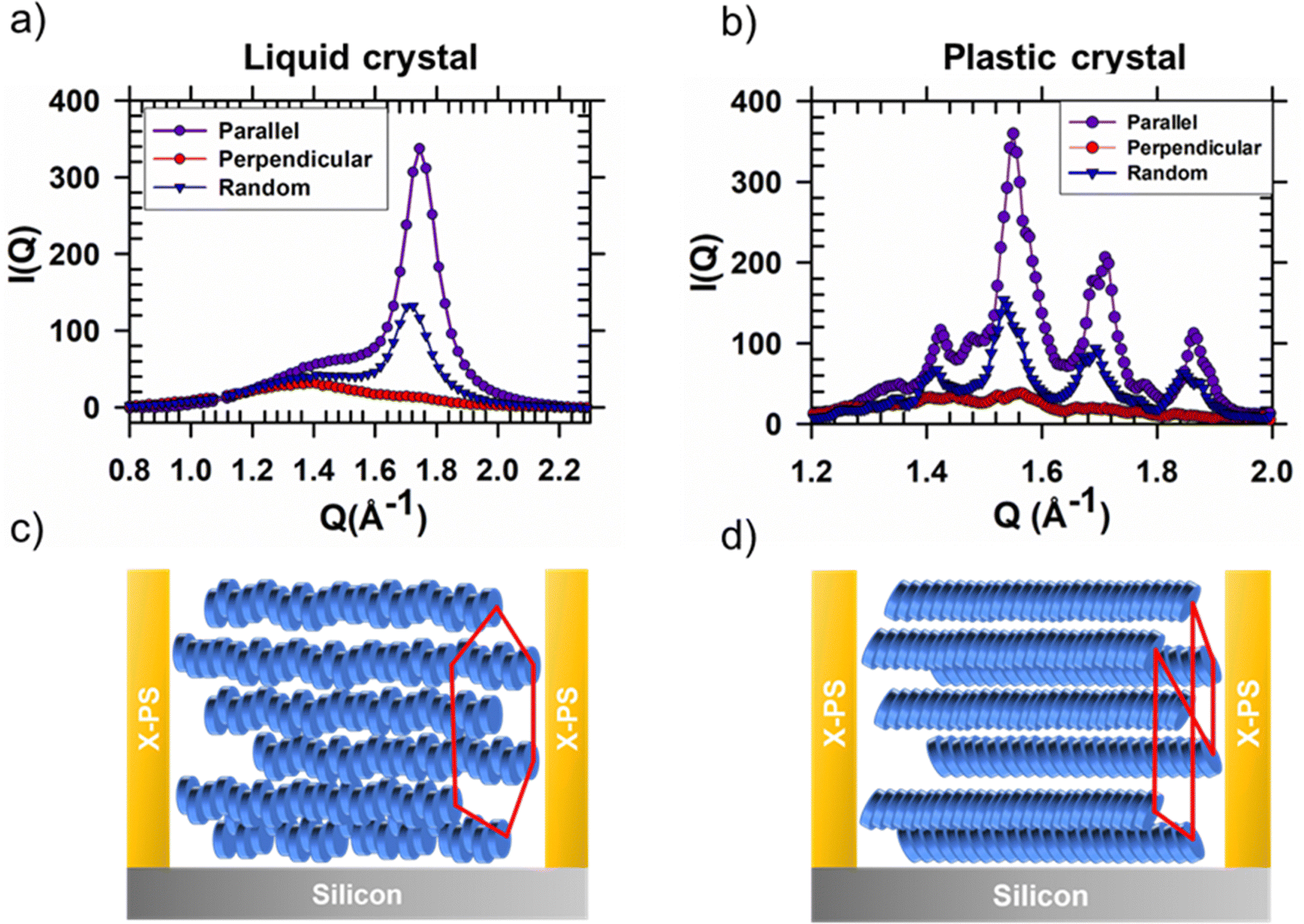 | ||
| Fig. 6 Scattering peaks arising from π-stacking interactions in HAT6 thin films in the liquid crystal and plastic crystal states. I(Q) vs. Q curves for (a) liquid crystal and (b) plastic crystal states on un-patterned (blue triangles) and patterned substrates with the X-ray beam parallel (purple circles) and perpendicular (red circles) to the X-PS gratings. X-ray scattering integrations are performed to capture π-stacking peaks. The films are between 50–60 nm in thickness. For the patterned sample, the width of the channels and pitch of the pattern are ≈8 μm and ≈10 μm, respectively. Schematic illustration of packing of discotic molecules in a microchannel in (c) the liquid crystal and (d) plastic crystal states. The π-stacking anisotropy in the liquid crystal state is transferred to the plastic crystalline phase. | ||
In the liquid crystalline phase of HAT6, molecules exhibit both edge-on packing and in-plane alignment in microchannels. Scattering patterns, collected with the microchannels parallel and perpendicular to the incoming X-ray beam are shown in Fig. 5. Characteristic of biaxial alignment, the scattered intensity varies with in-plane rotation.26 When the X-ray beam is parallel to the microchannels, the columnar peaks (spacing between columns) at Q ≈ 0.35 Å−1 nearly disappear and the intensity of the π-stacking peak at Qy ≈ 1.7 increases. The opposite effect is observed when the microchannels are perpendicular to the X-ray beam, indicating that the direction of π-stacking is perpendicular to the polystyrene walls. The intensity of the π-stacking peak for the un-patterned film, and for the patterned sample with the X-ray beam parallel and perpendicular to the X-PS walls is quantified in Fig. 6(a). The change in the intensity of the columnar peaks at Q ≈ 0.35 Å−1 with sample rotation is shown in Fig. S5 (ESI†). The liquid crystalline structure consistent with the scattering patterns from the film deposited on the patterned substrate is illustrated in Fig. 6(c).
When the DLC phase of HAT6 is aligned in-plane, the plastic crystalline state exhibits biaxial texture. Shown in Fig. 5(e) and (f) are the X-ray scattering patterns from HAT6 confined in microchannels, at room temperature and in its crystalline state. The cluster of crystal stacking peaks, at Q of 1.4–2.0 Å−1, which is bright when the X-ray is parallel to the microchannels almost completely disappears when the sample is rotated 90°. The change in scattered intensity with sample rotation is quantified in Fig. 6(b). The orientation of the columns in the plastic crystalline state confined in the microchannels is illustrated in Fig. 6(d).
Discussion
The present work challenges the view that crystallization of discotic liquid crystals leads to loss of optical anisotropy. Previous studies on DLC former HBC-C12 (hexakis-dodecyl-hexa-peri-hexabenzocoronene) showed that optical anisotropy can be switched off and on by transitioning between the crystalline and liquid crystalline states, respectively. The loss of optical anisotropy on cooling into the crystalline states was attributed to twisting of the conjugated cores upon solidification. Here, we do observe twisting of cores in the crystalline state but not loss of anisotropy. As shown in Fig. S6 and Table S2 (ESI†) a phase transition produces minimal change in optical texture. We observe, however, that the extent of anisotropy in the crystalline state is processing-dependent. As shown in Fig. S7 and Table S3 (ESI†), a crystalline sample prepared through quenching from the LC state exhibits significantly higher optical anisotropy than one prepared by slow cooling. It is therefore possible that HBC-C12 processed in the manner described in this manuscript would also exhibit optical anisotropy in its crystalline state.The results shown here establish that biaxiality can be transferred from an aligned DLC phase to the crystalline state. Confinement in microchannels is one of several methods to align DLCs. DLCs can also be aligned using magnetic fields27 or shear forces,28 and we expect the transfer of biaxiality to the crystalline state to occur irrespective of the method used to align the fluid phase. Fukushima and co-workers used shear forces to induce planar alignment of the DLC phase of a fluorinated triphenylene.29 Consistent with our observations, the authors observe transfer of biaxiality on crystallizing from the mesophase. The authors of the study use films that are ≈8 μm thick whereas we study films that are between 30–130 nm. The transfer of alignment from the discotic to crystalline phase is therefore possible across a broad thickness window. Moreover, the consistency between the results here and those of Fukushima and co-workers, where a different molecule was used, suggests the phenomenon observed here is not specific to a given molecule but rather could be applicable to a broad class of DLC formers.
One of the principal advantages of liquid crystals is the large volume over which they can be uniformly assembled. The largest lateral dimensions over which grapho-epitaxy of discotic liquid crystals has been achieved is 25 μm.18 We discussed earlier the broad thickness range over which DLCs can be aligned. The alignment attained over these large volumes can be transferred to the solid-state either through crystallization as reported here, or the mesophase structure can be frozen through photopolymerization. While the photopolymerization of mesophases has been extensively researched,30–32 the crystallization of DLCs as a route to prepare macroscopically organized solids has remained almost completely unexplored. Our work demonstrates the promise of using precursor liquid crystal phases to crystallize thin films of biaxial crystals over micrometer-length scales. The length scale over which grapho-epitaxy can be used to align DLCs and their crystals is comparable to channel lengths used in organic field effect transistors.33,34
Crystallization of molecular solids in nanoconfined geometries has been extensively studied.35,36 Confinement can influence crystal structure,37 polymorph selectivity,38 and lattice orientation.35 In our study, through crystallization of a discotic liquid crystal aligned in microchannels we gain control over crystal texture. The length scale of confinement differentiates the present study from previous work. Earlier studies of crystals grown from isotropic liquids have investigated texture in geometries where the confining dimension is ∼100 nm or less;35,39–41 the widths of the microchannels here are at-least an order of magnitude higher. Solidification from the liquid crystalline state therefore provides control of texture over much larger length scales than crystallization of confined isotropic liquids.
One of the questions that the present study raises is whether the transfer of alignment from the mesophase to the crystalline state would occur for liquid crystalline phases other than discotics. Several small molecule organic semiconductors exhibit smectic phases.42 Crystallization of smectic liquid crystals could also be used to organize molecular crystals over large length scales. Several molecules with a conjugated core, called chromonic LC formers,43 form lyotropic LC phases in water. Chromonic liquid crystalline phases can also be aligned on substrates with patterned topography.44 Crystallization of aligned chromonic LCs could be another avenue to form biaxial crystals from aligned mesophases. The organization and crystallization of mesogens with asymmetric side chain structure,45 such as Ph-BTBT-C10, in microchannels could also be an interesting research direction. It remains to be seen whether symmetric and asymmetric mesogens organize in a similar manner in microchannels.
Methods
Materials
HAT6 (2,3,6,7,10,11-Hexakis (hexyloxy) triphenylene) with an HPCL purity >98% was purchased from TCI (Tokoyo Chemical Industry) chemicals. Thermally cross-linkable polystyrene (X-PS; AZEMBLY NLD-128) was obtained from EMD Performance Materials. All chemicals were used as received.Sample preparation
The patterned areas for the POM and GIWAXS measurements were 1 mm × 1 mm and 1 cm × 1 cm, respectively. A larger area was patterned for GIWAXS measurements owing to the large beam footprint in the grazing incidence geometry.
Silicon channels
To promote photoresist adhesion, a monolayer of hexamethyldisilazane (HMDS) was deposited from the vapor phase onto an oxygen-plasma-cleaned silicon wafer. The positive photoresist AZ MiR 703 was spin-coated and the same photolithography and development process, described above was followed resulting in alternating regions of photoresist and exposed silicon. To etch the exposed silicon regions a CHF3/O2-based plasma was used under a pressure of 10 mTorr. The CHF3 and O2 flow rates were 35 sccm and 20 sccm, respectively. The RF (radiofrequency) and ICP (inductively coupled plasma) powers were 100 W and 300 W, respectively.After etching, the photoresist was stripped by sonicating in NMP (N-methylpyrrolidone) at 80 °C for 5 minutes. After sonication, the sample was rinsed with NMP, IPA (isopropyl alcohol), and H2O, and dried under N2 gas. Finally, the sample was cleaned using a 200 W oxygen plasma.
HAT6 spin-coating and thermal treatment
Solutions of HAT6 were prepared in chloroform and filtered with a 0.2 μm PTFE membrane prior to spin coating. The spin-coating speed and acceleration were 3000 rpm and 3000 rpm s−1, respectively. Spin-coated films were prepared on (1) cleaned, flat silicon (2) polystyrene gratings on silicon (3) topographically patterned silicon and (4) topographically patterned Au on silicon. After spin-coating, the samples were annealed at ≈105 °C for at least one minute to induce transition into the isotropic phase. The samples were then cooled to 90 °C to induce a transition to the discotic liquid crystalline phase. From 90 °C, the sample was rapidly quenched to room temperature, where HAT6 is a crystal. A metal block was used for quenching.For film thickness measurements, HAT6 was spin-coated on a clean, un-patterned silicon wafer and spectroscopic ellipsometry was performed. As it is not possible to directly measure the film thickness inside the grating with ellipsometry, the thicknesses reported in this manuscript are based on measurements performed on substitute silicon wafers. The thickness is calculated using the equation:
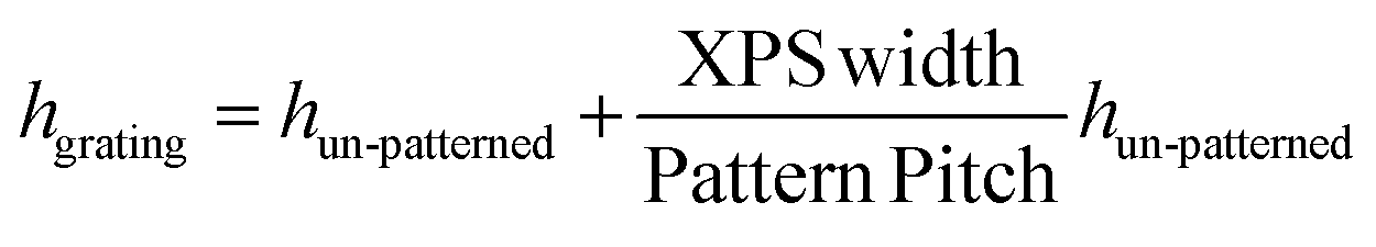
 describes the area fraction covered by XPS. In this calculation, we assume the material initially on top of X-PS migrates to the region below during annealing. AFM measurements of the thickness in the channel (Fig. S1, ESI†) are consistent with the thickness calculated using the above equation.
Microscopy
The optical microscopy images in Fig. 3 were collected between crossed polarizers in reflection mode using an Olympus BX51 microscope. Tapping mode atomic force microscopy was performed on a Bruker Multimode 5 instrument to obtain the images in Fig. 2. The image in Fig. S8b (ESI†) was acquired on a Carl Zeiss Merlin SEM instrument using an in-lens detector, an accelerating voltage of 3 keV and a working distance of ∼3 mm.GIWAXS
GIWAXS patterns were collected at Beamline 8-ID-E at the Advanced Photon Light source, Argonne National Lab. Diffraction patterns were collected using a photon energy of 10.9 KeV. An incidence angle of 0.14° was chosen for all reported measurements; this angle was chosen as it is above the typical critical angle of organic thin film but below the critical angle of the silicon substrate. The images were collected at a sample-to-detector distance of 217 mm using a Pilatus MF pixel array detector. The exposure time for the measurements was 2 s. To minimize beam damage and background air scatter, measurements were performed in a low vacuum chamber of ∼10−3 mbar.Prior to beamtime, the samples were subjected to the thermal treatment described above. For the un-patterned sample, a 5 °C min−1 heating rate was used in going from 25 °C (plastic crystal) to 80 °C (liquid crystal). For the grating samples, measurements were first performed at 25 °C with the X-ray beam perpendicular to the grating. The same was then heated to 80 °C at 5 °C min−1, and measurements were performed in the same geometry. The sample was then cooled to 25 °C at 5 °C min−1. The sample was rotated to make the gratings parallel to the X-ray beam. The same thermal protocol was then followed for the parallel geometry.
To produce the plot in 6a, the region from χ of 82° to 87° in the 2D pattern was integrated. For 6b, data from χ of 50° to 80° was integrated. Regions where there were no Bragg peaks were used to background subtract the 1D data shown in Fig. 6.
Differential scanning calorimetry
Differential scanning calorimetry was performed using the TA Instrument Discovery 2500. Both cooling and heating were performed at a rate of 10 °C min−1.Author contributions
K. B. and P. F. N. conceived and planned the experiments. Nanofabrication was performed by K. B. and W. C. X-ray measurements were performed by K. B., Z. J., J. S., and Z. W. Synthesis of TP6EO2M, described in the SI was performed by M. K. and C. E. All other experiments were performed by K. B. Data was analyzed by K. B. Paper was written by K. B. and T. E. J. J. d. P. and P. F. N. reviewed the paper before submission.Conflicts of interest
The authors declare no conflict of interest.Acknowledgements
We gratefully acknowledge support from the U.S. Department of Energy (DOE), Basic Energy Sciences, Materials Sciences and Engineering Division. This research used resources of the Advanced Photon Source; an Office of Science User Facility operated for the U.S. Department of Energy (DOE) by Argonne National Laboratory under contract no. DE-AC02-06CH11357. We acknowledge the MRSEC Shared User Facilities at the University of Chicago (NSF DMR-1420709). This work made use of the Pritzker Nanofabrication Facility of the Institute for Molecular Engineering at the University of Chicago, which receives support from Soft and Hybrid Nanotechnology Experimental (SHyNE) Resource (NSF ECCS-1542205), a node of the National Science Foundation's National Nanotechnology Coordinated Infrastructure. Parts of this work were carried out at the Soft Matter Characterization Facility of the University of Chicago.References
- H. Jiang and W. Hu, Angew. Chem., Int. Ed., 2020, 59, 1408–1428 CrossRef CAS PubMed.
- X. Zhang, H. Dong and W. Hu, Adv. Mater., 2018, 30, 1801048 CrossRef PubMed.
- J. Mei, Y. Diao, A. L. Appleton, L. Fang and Z. Bao, J. Am. Chem. Soc., 2013, 135, 6724–6746 CrossRef CAS PubMed.
- C. W. Sele, B. K. C. Kjellander, B. Niesen, M. J. Thornton, J. B. P. H. Van Der Putten, K. Myny, H. J. Wondergem, A. Moser, R. Resel, A. J. J. M. Van Breemen and others, Adv. Mater., 2009, 21, 4926–4931 CrossRef CAS PubMed.
- W. Pisula, A. Menon, M. Stepputat, I. Lieberwirth, U. Kolb, A. Tracz, H. Sirringhaus, T. Pakula and K. Müllen, Adv. Mater., 2005, 17, 684–689 CrossRef CAS.
- G. Giri, E. Verploegen, S. C. B. Mannsfeld, S. Atahan-Evrenk, D. H. Kim, S. Y. Lee, H. A. Becerril, A. Aspuru-Guzik, M. F. Toney and Z. Bao, Nature, 2011, 480, 504–508 CrossRef CAS PubMed.
- Y. Diao, B. C. K. Tee, G. Giri, J. Xu, D. H. Kim, H. A. Becerril, R. M. Stoltenberg, T. H. Lee, G. Xue, S. C. B. Mannsfeld and others, Nat. Mater., 2013, 12, 665–671 CrossRef CAS PubMed.
- J. Li, R. Xia, H. Xu, J. Yang, X. Zhang, J. Kougo, H. Lei, S. Dai, H. Huang, G. Zhang and others, J. Am. Chem. Soc., 2021, 143, 17857–17861 CrossRef CAS PubMed.
- T. Rozwadowski, M. Massalska-Arodź, Ł. Kolek, K. Grzybowska, A. Bak and K. Chłędowska, Cryst. Growth Des., 2015, 15, 2891–2900 CrossRef CAS.
- J. Piris, M. G. Debije, N. Stutzmann, B. W. Laursen, W. Pisula, M. D. Watson, T. Bjørnholm, K. Müllen and J. M. Warman, Adv. Funct. Mater., 2004, 14, 1053–1061 CrossRef CAS.
- J. Piris, W. Pisula, A. Tracz, T. Pakula, K. Müllen and J. M. Warman, Liq. Cryst., 2004, 31, 993–996 CrossRef CAS.
- T. Wöhrle, I. Wurzbach, J. Kirres, A. Kostidou, N. Kapernaum, J. Litterscheidt, J. C. Haenle, P. Staffeld, A. Baro, F. Giesselmann and others, Chem. Rev., 2016, 116, 1139–1241 CrossRef PubMed.
- S. Sergeyev, W. Pisula and Y. H. Geerts, Chem. Soc. Rev., 2007, 36, 1902–1929 RSC.
- A. M. van de Craats and J. M. Warman, Adv. Mater., 2001, 13, 130–133 CrossRef CAS.
- Z. An, J. Yu, S. C. Jones, S. Barlow, S. Yoo, B. Domercq, P. Prins, L. D. A. Siebbeles, B. Kippelen and S. R. Marder, Adv. Mater., 2005, 17, 2580–2583 CrossRef CAS.
- E. Juliana, C. Faria, H. Bock, H. Von Seggeren and I. Bechthold, Appl. Mater. Interfaces, 2013, 5, 11935–11943 CrossRef PubMed.
- S.-W. Kang, Q. Li, B. D. Chapman, R. Pindak, J. O. Cross, L. Li, M. Nakata and S. Kumar, Chem. Mater., 2007, 19, 5657–5663 CrossRef CAS.
- J. Cattle, P. Bao, J. P. Bramble, R. J. Bushby, S. D. Evans, J. E. Lydon and D. J. Tate, Adv. Funct. Mater., 2013, 23, 5997–6006 CrossRef CAS.
- A. M. van de Craats, J. M. Warman, A. Fechtenkötter, J. D. Brand, M. A. Harbison and K. Müllen, Adv. Mater., 1999, 11, 1469–1472 CrossRef CAS.
- A. Pipertzis, G. Zardalidis, K. Wunderlich, M. Klapper, K. Müllen and G. Floudas, Macromolecules, 2017, 50, 1981–1990 CrossRef CAS.
- L. Schmidt-Mende, A. Fechtenkotter, K. Mullen, E. Moons, R. H. Friend and J. D. MacKenzie, Science, 2001, 293, 1119–1122 CrossRef CAS PubMed.
- C. Krause, R. Zorn, F. Emmerling, J. Falkenhagen, B. Frick, P. Huber and A. Schönhals, Phys. Chem. Chem. Phys., 2014, 16, 7324–7333 RSC.
- I. G. Voigt-Martin, R. W. Garbella and M. Schumacher, Liq. Cryst., 1994, 17, 775–801 CrossRef CAS.
- K. Nickmans and A. P. H. J. Schenning, Adv. Mater., 2018, 30, 1703713 CrossRef PubMed.
- D. M. DeLongchamp, R. J. Kline, D. A. Fischer, L. J. Richter and M. F. Toney, Adv. Mater., 2011, 23, 319–337 CrossRef CAS PubMed.
- J. Rivnay, S. C. B. Mannsfeld, C. E. Miller, A. Salleo and M. F. Toney, Chem. Rev., 2012, 112, 5488–5519 CrossRef CAS PubMed.
- N. Boden, R. J. Bushby and J. Clements, J. Chem. Phys., 1993, 98, 5920–5931 CrossRef CAS.
- M. Yoshio, T. Mukai, H. Ohno and T. Kato, J. Am. Chem. Soc., 2004, 126, 994–995 CrossRef CAS PubMed.
- Y. Shoji, M. Kobayashi, A. Kosaka, R. Haruki, R. Kumai, S. Adachi, T. Kajitani and T. Fukushima, Chem. Sci., 2022, 13, 9891–9901 RSC.
- X. Feng, M. E. Tousley, M. G. Cowan, B. R. Wiesenauer, S. Nejati, Y. Choo, R. D. Noble, M. Elimelech, D. L. Gin and C. O. Osuji, ACS Nano, 2014, 8, 11977–11986 CrossRef CAS PubMed.
- X. Feng, K. Kawabata, M. G. Cowan, G. E. Dwulet, K. Toth, L. Sixdenier, A. Haji-Akbari, R. D. Noble, M. Elimelech, D. L. Gin and others, Nat. Mater., 2019, 18, 1235–1243 CrossRef CAS PubMed.
- X. Feng, S. Nejati, M. G. Cowan, M. E. Tousley, B. R. Wiesenauer, R. D. Noble, M. Elimelech, D. L. Gin and C. O. Osuji, ACS Nano, 2016, 10, 150–158 CrossRef CAS PubMed.
- S. Wang, M. Kappl, I. Liebewirth, M. Müller, K. Kirchhoff, W. Pisula and K. Müllen, Adv. Mater., 2012, 24, 417–420 CrossRef CAS PubMed.
- H. Bronstein, Z. Chen, R. S. Ashraf, W. Zhang, J. Du, J. R. Durrant, P. Shakya Tuladhar, K. Song, S. E. Watkins, Y. Geerts and others, J. Am. Chem. Soc., 2011, 133, 3272–3275 CrossRef CAS PubMed.
- Q. Jiang and M. D. Ward, Chem. Soc. Rev., 2014, 43, 2066–2079 RSC.
- F. C. Meldrum and C. O’Shaughnessy, Adv. Mater., 2020, 32, 2001068 CrossRef CAS PubMed.
- A. O. F. Jones, B. Chattopadhyay, Y. H. Geerts and R. Resel, Adv. Funct. Mater., 2016, 26, 2233–2255 CrossRef CAS.
- G. T. Rengarajan, D. Enke, M. Steinhart and M. Beiner, Phys. Chem. Chem. Phys., 2011, 13, 21367–21374 RSC.
- B. D. Hamilton, I. Weissbuch, M. Lahav, M. A. Hillmyer and M. D. Ward, J. Am. Chem. Soc., 2009, 131, 2588–2596 CrossRef CAS.
- Q. Jiang, C. Hu and M. D. Ward, J. Am. Chem. Soc., 2013, 135, 2144–2147 CrossRef CAS PubMed.
- J.-M. Ha, J. H. Wolf, M. A. Hillmyer and M. D. Ward, J. Am. Chem. Soc., 2004, 126, 3382–3383 CrossRef CAS.
- T. Kato, M. Yoshio, T. Ichikawa, B. Soberats, H. Ohno and M. Funahashi, Nat. Rev. Mater., 2017, 2, 1–20 Search PubMed.
- S.-W. Tam-Chang and L. Huang, Chem. Commun., 2008, 1957–1967 RSC.
- J. Y. Kim, K. Nayani, H. S. Jeong, H.-J. Jeon, H.-W. Yoo, E. H. Lee, J. O. Park, M. Srinivasarao and H.-T. Jung, Phys. Chem. Chem. Phys., 2016, 18, 10362–10366 RSC.
- H. Iino, T. Usui and J. Hanna, Nat. Commun., 2015, 6, 6828 CrossRef CAS PubMed.
Footnote |
| † Electronic supplementary information (ESI) available. See DOI: https://doi.org/10.1039/d3tc01175e |
| This journal is © The Royal Society of Chemistry 2023 |