
 Open Access Article
 This Open Access Article is licensed under a Creative Commons Attribution-Non Commercial 3.0 Unported Licence
Vector piezoelectric response and ferroelectric domain formation in Hf0.5Zr0.5O2 films†
Huan
Tan
,
Tingfeng
Song
,
Nico
Dix
 ,
Florencio
Sánchez
* and
Ignasi
Fina
*
,
Florencio
Sánchez
* and
Ignasi
Fina
*
Institut de Ciència de Materials de Barcelona (ICMAB-CSIC), Campus UAB, Bellaterra 08193, Barcelona, Spain. E-mail: fsanchez@icmab.es; ifina@icmab.es
First published on 10th May 2023
Abstract
The piezoelectric response in polycrystalline films of doped ferroelectric HfO2 has been explored so far; however, the lack of texture in most of the studied films prevents its full understanding. By selecting the appropriate substrate orientation, the ferroelectric orthorhombic phase ratio and crystallographic orientation can be modified in epitaxial films. We exploit this possibility to get further insight into the ferroelectric hafnium oxide piezoelectric response. While characterizing in-plane and out-of-plane piezoelectric responses, it is observed that their magnitude is mainly ruled by the presence of the orthorhombic phase and the polar axis of the polarization along the probing direction. It is also found for the as-grown state that along the out-of-plane direction a single ferroelectric domain is formed, and instead the in-plane response reveals a rich domain structure with a domain size of ≈10–30 nm. By characterizing the in-plane piezoelectric response, it is observed that it is anisotropic if the specific orientation, (110), of the SrTiO3 substrate is used. We propose that an out-of-plane single domain is formed due to the presence of an imprint electric field, whereas in-plane domains are formed by non-purely electrostatic interactions as revealed by their relatively large size. Besides, the small but sizeable in-plane anisotropic response is found to result from the in-plane crystallographic configuration, ultimately determined by the selected substrate.
 Ignasi Fina | Dr Ignasi Fina is a tenured scientist at Institut de Ciència de Materials de Barcelona from Consejo Superior de Investigaciones Científicas (ICMAB-CSIC). In 2012, he obtained his PhD studying single-phase and composite multiferroic films. He worked as Beatriu the Pinós fellow in Max Planck Institute of Microstructure Physics (Germany). He was also Juan de la Cierva and Ramon y Cajal fellow and he was awarded with the First Prize as Postdoctoral Investigator in the XXXVI meeting of the Real Sociedad Española de Física. He is the corresponding author of more than 50 publications and an author of over 120. His current research interests mainly focus on new ferroelectric materials for non-volatile memory devices. |
Introduction
Ferroelectric doped HfO2 is receiving technological interest for memory applications due to its CMOS compatibility. Beyond memory applications, it is also appealing to develop devices based on other functionalities such as piezoelectricity and pyroelectricity, inherently present in all ferroelectric materials. Pyroelectric and electrocaloric effects have been widely reported in polycrystalline ferroelectric doped HfO2 films.1–3 Piezoelectric response, on the other hand, has gotten less attention, until very recently when a negative piezoelectric response has been theoretically predicted4–6 and experimentally probed.6,7So far, most of the studies related to the piezoelectric response of ferroelectric doped HfO2 make use of the Piezoelectric Force Microscopy (PFM) tool. These studies mainly focus on the characterization of PFM loops and/or PFM images after electric lithography to further demonstrate the ferroelectric character of the material.8–10 More specific studies focus on the ferroelectric switching dynamics11,12 or ferroelectric retention.13 The findings in epitaxial ultrathin (≈≤ 2 nm) films are also relevant, where P–E loops in macroscopic devices and a ferroelectric PFM response have been observed.14,15 The coexistence of ferroelectric and paraelectric regions, which are attributed to the orthorhombic and monoclinic/cubic phases, respectively, has also been identified using PFM imaging.16,17 However, the crystalline grains of the various phases are of the same order as the normal PFM tip radii, making it challenging to distinguish among them.18,19 Additionally, quantification of the piezoelectric response using PFM is very limited, most probably due to the low piezoelectric response of the material (0.5–5.5 pm V−1) and the intrinsic difficulties of quantification related to its very insulating character.16,20 Note that the clamping effect produced by the presence of coexisting non-ferroelectric phases with lower piezoelectric response can reduce the out-of-plane deformation, whereas the presence of the substrate clamps the in-plane deformation.21,22
Despite the listed difficulties, the characterization of the out-of-plane and in-plane piezoelectric response is of relevance for several applications. F.i., regarding in-plane responses, in layered strain-mediated magnetoelectric systems composed of a ferroelectric and a magnetic material, the in-plane deformation of the ferroelectric layer (controlled by an external electric field) dictates the magnetization of an adjacent magnetic material.23 In particular, in-plane anisotropic piezoelectric effects can result in the in-plane rotation of the magnetization, which can lead to the observation of large magnetoelectric coupling effects.24–28 However, in polycrystalline HfO2 films, the in-plane response must be isotropic. Instead, in epitaxial films, the control of the in-plane and out-of-plane crystalline orientations is possible by the use of appropriate substrates, allowing in-plane anisotropic piezoelectric effects. Besides, there are no systematic studies on the as-grown ferroelectric domain development in ferroelectric HfO2, despite the fact that they would aid in a better understanding of the mechanisms underlying ferroelectric responses.
Hf0.5Zr0.5O2 (HZO) epitaxial films on La2/3Sr1/3MnO3(LSMO)/SrTiO3(001) show (111) out-of-plane texture and therefore polarization is tilted by 54.7° with respect to the out-of-plane direction with three possible orientations (Fig. 1(a)) and three possible in-plane orientations rotated by 120° are possible. In addition, 4 in-plane crystalline variants rotated by 90° appear (Fig. 1(c)), and thus polarization shows 12 possible directions.29 In films grown of LSMO/SrTiO3(110), (111) out-of-plane texture is present with also three possible polar directions (Fig. 1(a)), but two sets of 2 crystalline variants separated by only 8.5° are formed. Each of these two sets is separated by 180° (Fig. 1(d)).30 Finally, films on LSMO/SrTiO3(111) show tilted epitaxy with one of the orthorhombic cell axes parallel to the [0–11] axes of the substrate and the other two at 24° and 66° away from the out-of-plane direction (Fig. 1(b)). Three crystalline variants are present in this case separated by 120° (Fig. 1(e)).31 Thus, the in-plane response along perpendicular directions, in films grown on LSMO/SrTiO3(110) and (111), is expected to be anisotropic (Fig. 1(d and e)), but not on films grown on LSMO/SrTiO3(001). In addition, an in-plane response is expected to depend on the orthorhombic phase ratio, the presence of which is also tailored by the selected substrate orientation.29–31
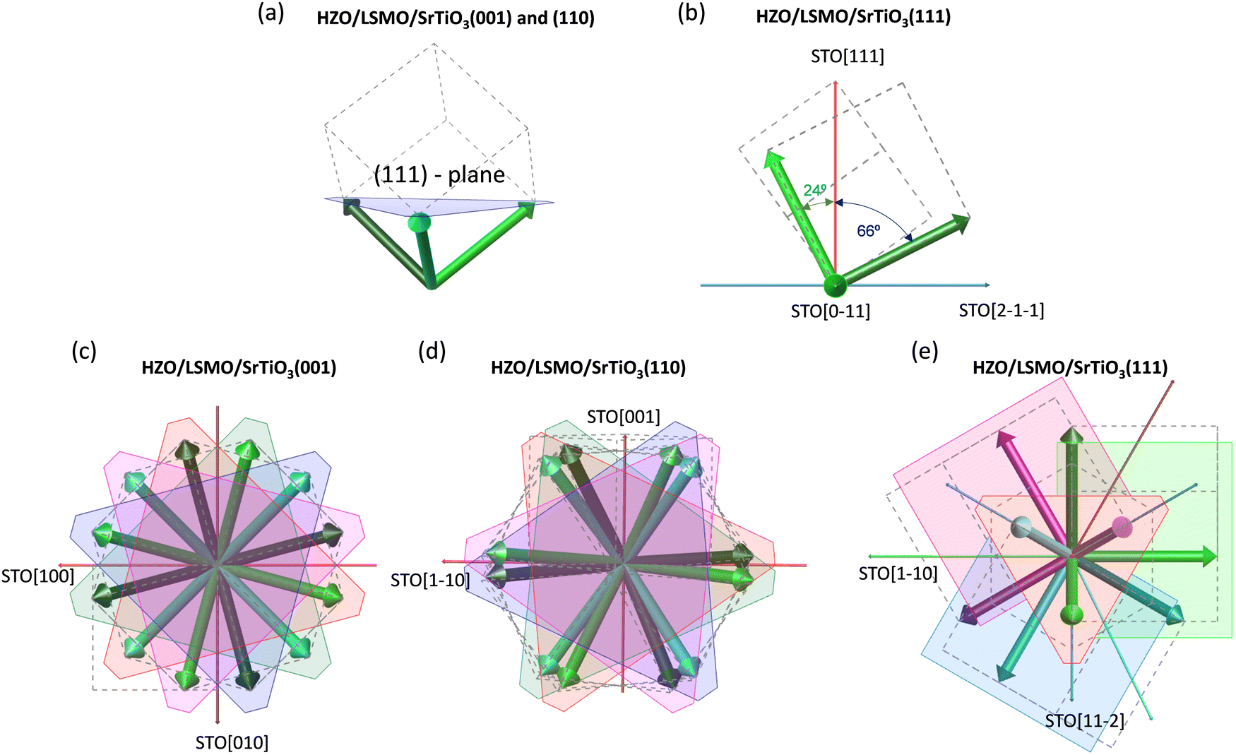 | ||
| Fig. 1 (a and b) Sketch of the out-of-plane crystallographic orientation of orthorhombic HZO films grown on (a) LSMO/SrTiO3(001) and LSMO/SrTiO3(110), and (b) LSMO/SrTiO3(111) corresponding to one of the crystalline variants. (c–e) Sketch of all the possible in-plane directions of the polar axis of orthorhombic HZO films grown on LSMO/SrTiO3(001), LSMO/SrTiO3(110), and LSMO/SrTiO3(111), respectively. Axes are along the two in-plane orientations of the substrate along its edges. In (c–e) each crystalline variant is indicated by a different color. | ||
In this work, we characterize the out-of-plane and in-plane piezoelectric response of HZO epitaxial films grown on LSMO/SrTiO3 (001), (110) and (111). It turns out that the piezoelectric responses from individual grains cannot be disentangled and therefore distinguishing isolated contributions from grains with different phases or orientations is not possible. Instead, the out-of-plane and in-plane piezoelectric response magnitude is found to be mainly determined by the fraction of the orthorhombic phase and the projection of the polarization along the probing direction. Characterization of the in-plane piezoelectric response of the as-grown state allows the identification of the presence of in-plane ferroelectric domains with sizes ranging from 10 to 30 nm, contrary to what is observed along the out-of-plane direction where Eimp field imposes the as-grown state to be towards the bottom electrode. As expected, these in-plane ferroelectric domains are not switchable under the application of an out-of-plane external electric field. Finally, it is also shown that the in-plane piezoelectric response is sizeable and anisotropic in films grown on LSMO/SrTiO3(110).
Materials and methods
Epitaxial HZO films (t = 6.5 nm) were grown on LSMO (t = 25 nm) buffered SrTiO3(001), SrTiO3(110) and SrTiO3(111) substrates (see sketch of the structures in Fig. 2(a–c)), by pulsed laser deposition (KrF excimer laser, 248 nm wavelength). Further details of the deposition conditions are reported elsewhere.29–31 Platinum circular top electrodes with a thickness of 20 nm and a diameter of 20 μm were deposited ex situ by sputtering through stencil masks at room temperature and were used to perform macroscopic ferroelectric characterization.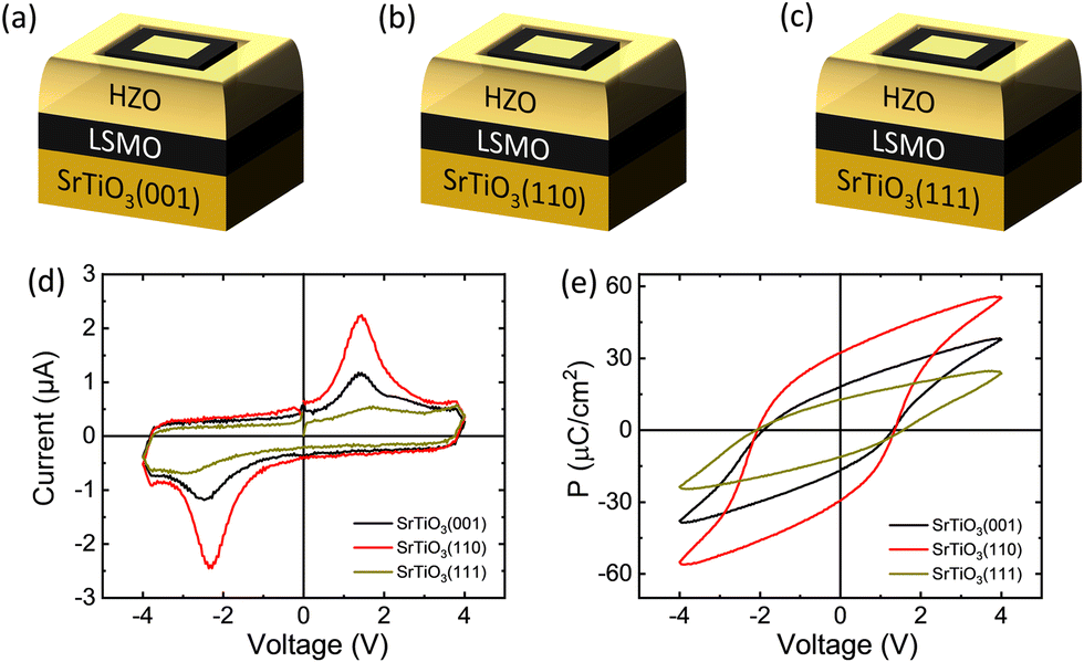 | ||
| Fig. 2 (a–c) Sketch of HZO films grown on LSMO/SrTiO3(001), LSMO/SrTiO3(110), and LSMO/SrTiO3(111), respectively. (d and e) Corresponding I–V and P–V loops measured at 1 kHz for the three samples. | ||
Piezoelectric force microscope (PFM) measurements were performed with an MFP-3D microscope (Oxford Instrument Co.) using the BudgetSensors silicon (n-type) probe with Pt coating (Multi75E-G). The typical tip radius is less than 25 nm and the spring constant is ∼3 N m−1. PFM electric lithography was used to test the switchable polarization. As sketched in Fig. 2(a–c), in the dark region, −8 V is applied and in the inner bright region, +8 V. In the outer bright region, no voltage was applied, and thus it corresponds to the as-grown state. To achieve better sensitivity, the dual AC resonance tracking (DART) method was employed to read the out-of-plane state after electric lithography.32 For as-grown domain imaging, single-frequency vector PFM was also employed. Piezoelectric response is evaluated at near resonance in the same conditions in all the cases, and thus the amplitude magnitude is comparable for all characterizations, but it does not correspond to the intrinsic piezoelectric response and thus it cannot be used to quantify it.33 Single-frequency vector PFM mode was used to obtain the in-plane domain images and out-of-plane simultaneously. The in-plane component of the piezoresponse is evaluated by the lateral deflection of the AFM cantilever, which is perpendicular to the longest cantilever direction. When probing the in-plane piezoresponse along perpendicular directions, the sample is physically rotated by 90°, and thus the imaged region is another. The out-of-plane piezoresponse is evaluated by the vertical deflection of the AFM cantilever. Recall here that for ferroelectric domains with the polar axis pointing in the opposite direction along the normal to the sample surface (for out-of-plane response)34 or along the perpendicular direction of the cantilever longest side (for in-plane response), the amplitude signal is expected to be constant with zero signal at the domain walls, and the phase signal is expected to show 180° contrast. Note also that single-frequency vector PFM and DART images are collected at different frequencies; therefore the amplitude signals are not comparable. Atomic force microscopy (AFM) in dynamic mode was used to characterize the surface morphology in separate experiments, and thus these are representative but do not correspond to the same region of the PFM images.
An AixACCT TFAnalyser2000 platform was used to measure ferroelectric polarization loops at room temperature. Current versus voltage (I–V) loops were measured at 1 kHz by the dynamic leakage current compensation (DLCC) procedure and positive-up negative-down (PUND) modes in top-bottom configuration with the bottom LSMO electrode grounded. From both measurement methods, the polarization loops confirm that the HZO films on different crystalline oriented substrates are ferroelectric. In Fig. 2(d and e), the current versus voltage (I–V) and polarization versus voltage (P–V) loops, respectively, of the HZO films grown on LSMO/SrTiO3(001), LSMO/SrTiO3(110), and LSMO/SrTiO3(111) are shown. The remanent polarization (Pr) is 18 μC cm−2, 32 μC cm−2 and 12 μC cm−2 for HZO/LSMO/STO (001), HZO/LSMO/STO (110) and HZO/LSMO/STO (111), respectively. From the obtained Pr values and from the fact that Pr is correlated with the quantity of the orthorhombic phase,35 it can be estimated that the amount of orthorhombic phase is 56, 100 and 55%, respectively (see S1 of ESI†). Note that monoclinic and orthorhombic grains have a columnar shape, as characterized by scanning transmission electron microscopy, elsewhere.30,31,36 The imprint electric field (Eimp) values are −800.0 kV cm−1, −861.5 kV cm−1 and −738.5 kV cm−1 for HZO/LSMO/STO (001), HZO/LSMO/STO (110) and HZO/LSMO/STO (111), respectively, thus similar and always pointing towards LSMO. Corresponding PUND loops are shown in S2 of the ESI,† showing slightly lower Pr values but displaying the same trend.
Results
Fig. 3(a–c) show archetypical PFM phase images collected in DART mode with 180° phase contrast between inner regions poled with −8 V (Pup, away from the bottom electrode) and with +8 V (Pdown, towards the bottom electrode) revealing the ferroelectric nature of the films. The outer region corresponds to the as-grown state, in all cases, Pdown. This agrees with the negative internal Eimp inferred from the P–V loops (Fig. 2(d and e)), which indicates that the Pdown state is favored. The corresponding PFM amplitude images (Fig. 3(d–f)) show small contrast between the Pdown and Pup regions and a decrease of the response at their boundary, except in some regions where likely charging effects are more relevant.37 The PFM amplitude decrease at the domain walls is less visible in the sample on LSMO/SrTiO3(110), although it is present, probably due to its better insulating character30 in front of films grown on LSMO/SrTiO3(001)29 resulting in larger charging effects.16 The amplitude PFM signal seems at first sight very similar in the three samples in the as-grown state. More precise comparison of the out-of-plane amplitude PFM signal can be done by inspection of images collected using vector PFM of the as-grown state and shown in S3 of the ESI,† where it can be concluded that the film on LSMO/SrTiO3(110) shows larger response in agreement with the larger fraction of orthorhombic phase30 and the larger Pr of this film (Pr = 32 μC cm−2). A smaller response is found for the film on LSMO/SrTiO3 (001) and slightly smaller for the film on (111), in agreement with the fact that these show Pr = 18 μC cm−2 and 12 μC cm−2, respectively. In addition, note that the histogram of the as-grown state (ESI† S2), only shows 1 contribution, indicating that the contribution from monoclinic and orthorhombic grains for all the samples or from the orthorhombic grains with different polarization direction for the LSMO/SrTiO3(111) sample, cannot be distinguished. Therefore, different contrast in the PFM amplitude image can only be ascribed to gradients of response resulting from convolution of different contributions.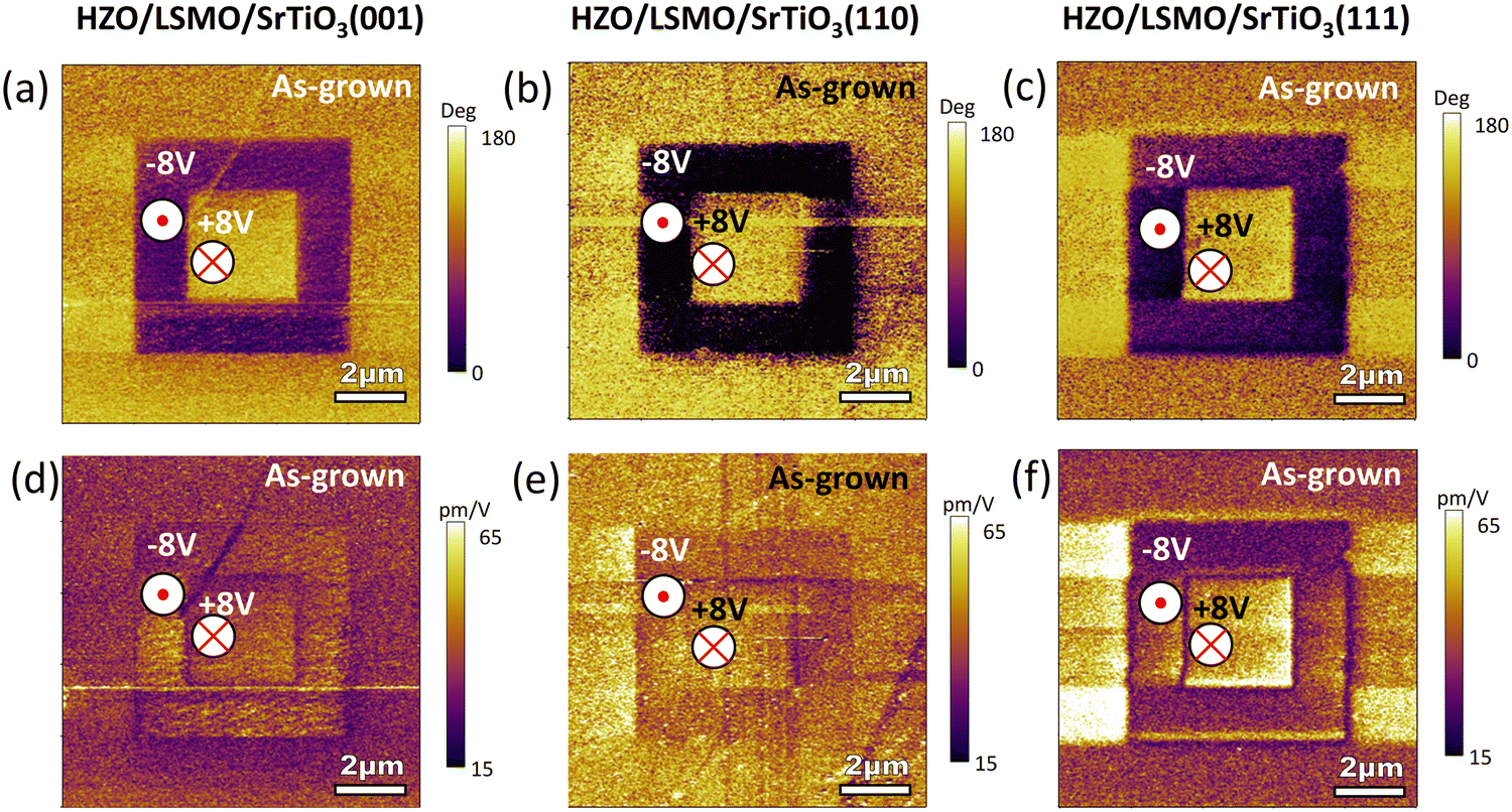 | ||
| Fig. 3 (a–c) PFM out-of-plane phase images for the three HZO films grown on LSMO/SrTiO3(001), LSMO/SrTiO3(110), and LSMO/SrTiO3(111), respectively, after applying +(−)8 V in the bright (dark) regions. The outer region corresponds to the as-grown state and no voltage has been applied. (d–f) PFM out-of-plane amplitude images corresponding to the (a–c) phase image regions. | ||
Now we turn to the analysis of the in-plane piezoelectric response. In Fig. 4(a–c), the PFM phase images of the as-grown state reveal the presence of domains with opposite in-plane orientation (towards the top and towards the bottom part of the image). Note that the particular polarization sign for the bright or dark regions cannot be inferred due to the absence of a reference region.7 Similar shapes are observed if deflection along the perpendicular axis is probed (Fig. 4(d–f)). The domains have a maze-like shape with lateral lengths between 10 and 100 nm or larger. Note also the similar total fraction of domains pointing along opposite directions in the three samples as expected due to the absence of preferential sign for the in-plane ferroelectric polarization. Finally, it is also emphasized that there is no dependence of the domain shape orientation depending on the different used substrate. This is expected for the film grown on LSMO/SrTiO3(001), due to the in-plane perpendicular directions being equivalent, but not necessarily for the films on (110) and LSMO/SrTiO3(111). In Fig. 4(g–i), the in-plane signal collected after prepoling with the indicated voltage is shown. Inner and outer regions do not show significant contrast. Therefore, as expected by the fact that the applied electric field is perpendicular to the in-plane polarization direction, the out-of-plane external electric stimuli do not result in a modification of the in-plane domain configuration contrary to the out-of-plane case (Fig. 3). Note that as-grown in-plane ferroelectric domains are not distinguishable due to the larger size of the image compared to Fig. 4(a–f).
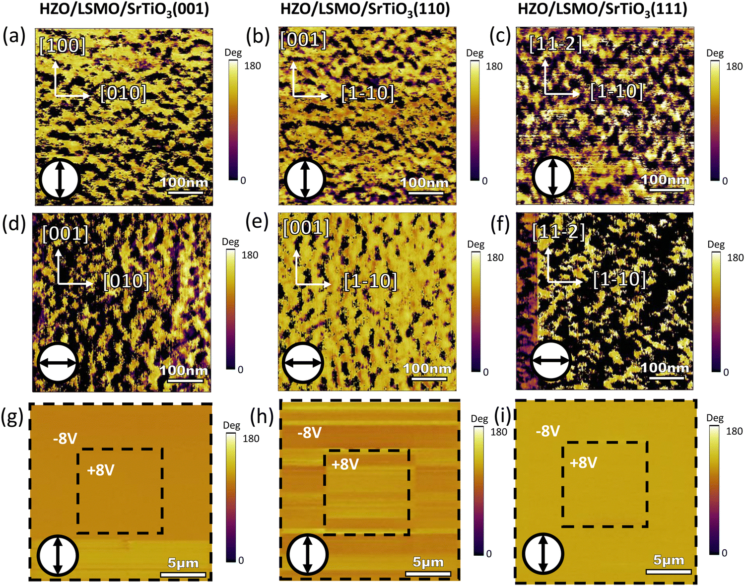 | ||
| Fig. 4 (a–c) PFM in-plane phase images for the three HZO films grown on LSMO/SrTiO3(001), LSMO/SrTiO3(110), and LSMO/SrTiO3(111), respectively. Response is probed along the vertical in-plane direction as indicated in the inset. (d–f) Idem, while probing along the horizontal in-plane direction. (g–i) PFM in-plane phase images for the three HZO films after applying + and −8 V in the inner and outer regions as indicated. The in-plane substrate orientation in (g–i) is the same as in (a–c). | ||
Further information on the in-plane PFM response can be obtained by analyzing the in-plane PFM amplitude images shown in Fig. 5. In Fig. 5(a–c), the amplitude PFM image of the as-grown state for the films grown on LSMO/SrTiO3(001), (110) and (111), respectively, is shown. Grainy morphology is here observed with similar grain size around 10–30 nm for the three films. The insets correspond to the topographic images (same scale) showing smaller grain size. Therefore, the collected PFM response corresponds to the convolution of different grains with different orientation and/or phases. The different size of the grains/domains in the topography/PFM images also disregards important cross-talk effects of topography in the collected amplitude images. We do also observe in the PFM amplitude image that different domains show different piezoresponse amplitude, as denoted by their different brightness. This can be ascribed to the fact that the response is modulated by the different presence of the orthorhombic phase. But the response of the out-of-plane piezoelectric amplitude shows less contrast among grains (see S3 of the ESI†). Therefore, the different amplitude response likely corresponds to a convolution of the different direction of the polarization added to the presence of monoclinic grains with lower response, as discussed in more detail in the discussion section. When the piezoresponse is probed along the perpendicular orientation (Fig. 5(d–f)), a significant amount of brighter grains for the film grown on LSMO/SrTiO3(110) (Fig. 5(d)) is observed.
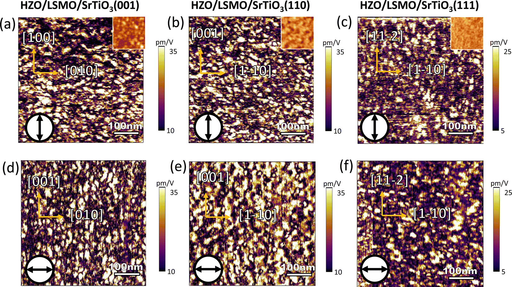 | ||
| Fig. 5 (a–c) PFM in-plane amplitude images for the HZO films on LSMO/SrTiO3(001), LSMO/SrTiO3(110), and LSMO/SrTiO3(111), respectively. Response is probed along the vertical direction as indicated in the bottom-left. Top-right insets show the topography images. (d–f) Idem, while probing along the horizontal direction. | ||
To better visualize the different amplitude in-plane response depending on the probed direction for the three films, histograms of the PFM amplitude images of the six 500 × 500 nm2 regions shown in Fig. 5 are presented in Fig. 6. In Fig. 6(a), it can be observed that for the film on LSMO/SrTiO3(001), the response is similar irrespective of the probed direction, SrTiO3[010] or [100]. Instead, in Fig. 6(b), a strong different amplitude distribution can be observed for the film on LSMO/SrTiO3(110), despite the similar position of its maxima. In particular, more grains of larger amplitude response are observed when probing along the SrTiO3[1–10] direction than for the [001] one. Finally, for the film on LSMO/SrTiO3(111) (Fig. 6(c)), the maxima of the histograms occur at similar positions while probing along the SrTiO3[1–10] or the [11–2] directions.
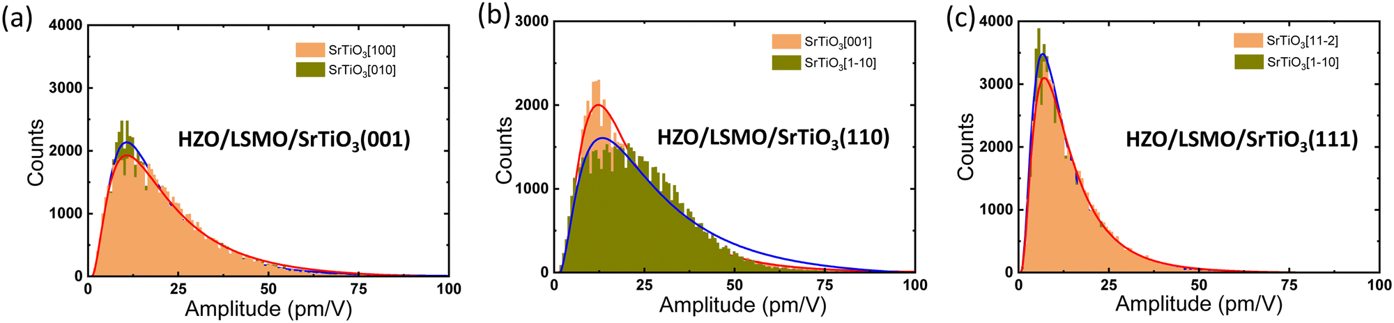 | ||
| Fig. 6 (a–c) Histograms of the PFM out-of-plane amplitude images for the three HZO films grown on LSMO/SrTiO3(001), LSMO/SrTiO3(110), and LSMO/SrTiO3(111), respectively, along the indicated directions. The line above the histogram corresponds to lognormal fitting. | ||
Discussion
The main results of this study are summarized in Fig. 7(a). The center of the lognormal distribution for the out-of-plane (see S3 of ESI†) and in-plane (Fig. 6) directions of the films is plotted (left-axis), together with the remanent polarization value (right axis), as a function of the SrTiO3 substrate orientation. It can be observed that the out-of-plane and in-plane PFM amplitude scales with the remanent polarization, and therefore with the amount of orthorhombic phase.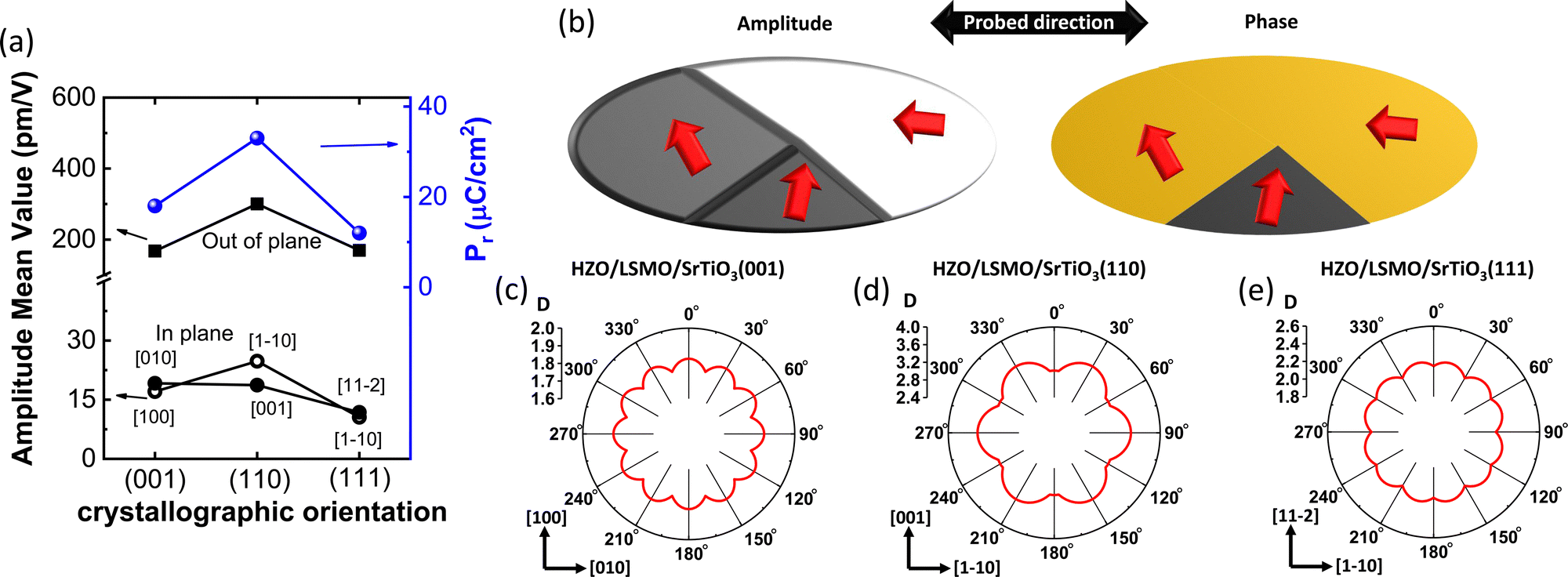 | ||
| Fig. 7 (a) Out-of-plane and in-plane amplitude piezoelectric response dependence on the substrate crystallographic orientation. (b) Sketch of the expected in-plane PFM amplitude (left) and phase (right) responses if the probed direction is horizontal in the presence of ferroelectric domains with different in-plane orientations as indicated by the red arrows. (c–e) In-plane amplitude piezoelectric response dependence on the scanning probing direction for the HZO films grown on LSMO/SrTiO3(001), LSMO/SrTiO3(110), and LSMO/SrTiO3(111), respectively. | ||
From the analysis of vector PFM images of the as-grown state, it is found that the films are fully downwards polarized with a single out-of-plane domain, in agreement with the Eimp direction inferred from ferroelectric characterization using macroscopic top electrodes (Fig. 2). In addition, all the films show maze-like shape in the in-plane phase images with the size of domains of around 10–100 nm, whereas the amplitude images show grainy shapes with sizes of around 10–30 nm. The different domain distribution of the in-plane and out-of-plane images can be explained by the fact that the phase can only be 0 or 180°, depending on the sign of the projection of the polarization vector, and that the amplitude signal depends on the amplitude of the in-plane polarization, but also on the amplitude of its projection along the probing direction. Fig. 7(b) shows a schematic example of the PFM amplitude and phase image of three domains when the piezoresponse is probed along the horizontal direction. The amplitude response displays three regions because the projection along the probing direction is different for each of the domains, in contrast to the phase response only displaying two regions. Therefore, the number of distinguishable domains by phase is always less than by amplitude. The effective amplitude images are shown in S4 of the ESI,† where Aeff = A![[thin space (1/6-em)]](https://www.rsc.org/images/entities/char_2009.gif) sin(Φ) is plotted, where A is the amplitude and Φ is the phase of the PFM signal helping to better visualize the different polarization direction of the domains. However, one should also consider that the contribution of the monoclinic grains can also affect the image contrast, as discussed as follows. In out-of-plane amplitude images (see S3 of ESI†), it can be observed that different grains also show different amplitude response, although the image is more uniform, and the signal between grains is not zero as a result of the fact that the polarization is pointing along a single (downwards) direction and therefore ferroelectric domain walls are not present. More precisely, polarization points 54.7° away from the normal direction and therefore its projection along the out-of-plane direction is always the same. Thus, the different contrast in the out-of-plane images only results from the presence of grains with different response, i.e. presence of non-ferroelectric phase. The contrast being larger in in-plane image data suggests that the different polarization direction of domains and the presence of monoclinic phase contributions coexist in the in-plane response. In archetypical ferroelectrics, square periodicity (w2) of domains is found to be similar to the ferroelectric thickness according to Kittel's law.38 Characterized films are around 6 nm thick and domains are 10–30 nm in width. Therefore, it can be concluded that the size of the domains with polarization pointing in-plane is larger than those determined by the electrostatic boundary conditions. The fact that ferroelastic domains are typically found to be larger than non-ferroelastic ones39 indicates that the observed large domain size probably results from ferroelastic interactions.
sin(Φ) is plotted, where A is the amplitude and Φ is the phase of the PFM signal helping to better visualize the different polarization direction of the domains. However, one should also consider that the contribution of the monoclinic grains can also affect the image contrast, as discussed as follows. In out-of-plane amplitude images (see S3 of ESI†), it can be observed that different grains also show different amplitude response, although the image is more uniform, and the signal between grains is not zero as a result of the fact that the polarization is pointing along a single (downwards) direction and therefore ferroelectric domain walls are not present. More precisely, polarization points 54.7° away from the normal direction and therefore its projection along the out-of-plane direction is always the same. Thus, the different contrast in the out-of-plane images only results from the presence of grains with different response, i.e. presence of non-ferroelectric phase. The contrast being larger in in-plane image data suggests that the different polarization direction of domains and the presence of monoclinic phase contributions coexist in the in-plane response. In archetypical ferroelectrics, square periodicity (w2) of domains is found to be similar to the ferroelectric thickness according to Kittel's law.38 Characterized films are around 6 nm thick and domains are 10–30 nm in width. Therefore, it can be concluded that the size of the domains with polarization pointing in-plane is larger than those determined by the electrostatic boundary conditions. The fact that ferroelastic domains are typically found to be larger than non-ferroelastic ones39 indicates that the observed large domain size probably results from ferroelastic interactions.
In-plane asymmetric piezoresponse is only observed in the film grown on LSMO/SrTiO3(110), with larger response along [1–10] compared with the [001]. As anticipated in the introduction, in films grown on LSMO/SrTiO3(110) and (111), an asymmetric response could be expected. In Fig. 7(c–e), the calculated projected sum of all possible polarization directions with the polarization normalized to its theoretical value (D)40,41 for all the possible probing directions on the three HZO films grown on LSMO/SrTiO3(001), (110) and (111), respectively, is shown. Equations to calculate the projection of the polarization are shown in S5 of the ESI.† The contrast along the perpendicular directions (SrTiO3[001] and [1–10]) is the largest for the film on LSMO/SrTiO3(110) (Fig. 7(d)). In the film grown on LSMO/SrTiO3(111), asymmetry in the in-plane response along the perpendicular [11–2] and [1–10] directions is also expected (Fig. 7(e)). However, the modulation in absolute values is smaller than in the case of the film grown on LSMO/SrTiO3(110), which is most probably the origin of the lack of clear observation of the in-plane anisotropy by PFM. In the film grown on LSMO/SrTiO3(001), the same response along the perpendicular in-plane directions should be expected (Fig. 7(c)), as found.
Conclusions
The out-of-plane and in-plane piezoelectric response of HZO films with different crystalline orientations has revealed that the magnitude of both signals is mainly ruled by the amount of orthorhombic phase ratio and the projection of the polar axis along the probing direction. The signal from individual grains is not distinguishable due to their small size. The ferroelectric domain structure in the as-grown state characterization shows that, whereas a single ferroelectric domain is found along the out-of-plane direction, in-plane domains with size in disagreement with Kittel's law are present. Therefore, it has been concluded that the out-of-plane polarization state is mainly driven by the presence of built-in electric fields (Eimp) and the in-plane domain configuration by non-purely electrostatic interactions. It has also been concluded that the impact of the in-plane crystallographic orientations of the HZO variants on the in-plane piezoelectric response is sizeable. The results presented here, where epitaxial films with tuned crystalline orientation are reported, entail a major step of fundamental interest to reveal the tensorial piezoelectric response of ferroelectric doped HfO2 and for applications where elastic coupling and mechanical stress can largely have a positive or negative impact on functional properties.Conflicts of interest
There are no conflicts to declare.Acknowledgements
Financial support from the Spanish Ministry of Science and Innovation (MCIN/AEI/10.13039/501100011033), through the Severo Ochoa FUNFUTURE (CEX2019-000917-S), PID2020-112548RB-I00 and PID2019-107727RB-I00 projects program and from Generalitat de Catalunya (2021 SGR 00804) is acknowledged. We also acknowledge project TED2021-130453B-C21, funded by MCIN/AEI/10.13039/501100011033 and European Union NextGeneration EU/PRTR. HT is financially supported by China Scholarship Council (CSC) with no. 201906050014. The work of HT has been done as part of his PhD program in Materials Science at Universitat Autònoma de Barcelona.References
- M. H. Park, H. J. Kim, Y. J. Kim, T. Moon and C. S. Hwang, Appl. Phys. Lett., 2014, 104, 072901 CrossRef.
- M. H. Park, H. J. Kim, Y. J. Kim, T. Moon, K. D. Kim and C. S. Hwang, Nano Energy, 2015, 12, 131–140 CrossRef CAS.
- M. Hoffmann, U. Schroeder, C. Künneth, A. Kersch, S. Starschich, U. Böttger and T. Mikolajick, Nano Energy, 2015, 18, 154–164 CrossRef CAS.
- J. Liu, S. Liu, L. H. Liu, B. Hanrahan and S. T. Pantelides, Phys. Rev. Appl., 2019, 12, 034032 CrossRef CAS.
- J. Liu, S. Liu, J.-Y. Yang and L. Liu, Phys. Rev. Lett., 2020, 125, 197601 CrossRef CAS PubMed.
- S. Dutta, P. Buragohain, S. Glinsek, C. Richter, H. Aramberri, H. Lu, U. Schroeder, E. Defay, A. Gruverman and J. Íñiguez, Nat. Commun., 2021, 12, 7301 CrossRef CAS PubMed.
- P. Buragohain, H. Lu, C. Richter, T. Schenk, P. Kariuki, S. Glinsek, H. Funakubo, J. Íñiguez, E. Defay, U. Schroeder and A. Gruverman, Adv. Mater., 2022, 34, 2206237 CrossRef CAS PubMed.
- A. Chernikova, M. Kozodaev, A. Markeev, D. Negrov, M. Spiridonov, S. Zarubin, O. Bak, P. Buragohain, H. Lu and E. Suvorova, ACS Appl. Mater. Interf., 2016, 8, 7232–7237 CrossRef CAS PubMed.
- A. Chouprik, S. Zakharchenko, M. Spiridonov, S. Zarubin, A. Chernikova, R. Kirtaev, P. Buragohain, A. Gruverman, A. Zenkevich and D. Negrov, ACS Appl. Mater. Interf., 2018, 10, 8818–8826 CrossRef CAS PubMed.
- S. S. Cheema, D. Kwon, N. Shanker, R. dos Reis, S.-L. Hsu, J. Xiao, H. Zhang, R. Wagner, A. Datar, M. R. McCarter, C. R. Serrao, A. K. Yadav, G. Karbasian, C.-H. Hsu, A. J. Tan, L.-C. Wang, V. Thakare, X. Zhang, A. Mehta, E. Karapetrova, R. V. Chopdekar, P. Shafer, E. Arenholz, C. Hu, R. Proksch, R. Ramesh, J. Ciston and S. Salahuddin, Nature, 2020, 580, 478–482 CrossRef CAS PubMed.
- P. Buragohain, A. Erickson, T. Mimura, T. Shimizu, H. Funakubo and A. Gruverman, Adv. Funct. Mater., 2021, 32, 2108876 CrossRef.
- P. Buragohain, C. Richter, T. Schenk, H. Lu, T. Mikolajick, U. Schroeder and A. Gruverman, Appl. Phys. Lett., 2018, 112, 222901 CrossRef.
- A. Chouprik, E. Kondratyuk, V. Mikheev, Y. Matveyev, M. Spiridonov, A. Chernikova, M. G. Kozodaev, A. M. Markeev, A. Zenkevich and D. Negrov, Acta Mater., 2021, 204, 116515 CrossRef CAS.
- M. Cervo Sulzbach, H. Tan, S. Estandía, J. Gàzquez, F. Sánchez, I. Fina and J. Fontcuberta, ACS Appl. Electron. Mater., 2021, 3, 3657–3666 CrossRef CAS.
- B. Prasad, V. Thakare, A. Kalitsov, Z. Zhang, B. Terris and R. Ramesh, Adv. Electron. Mater., 2021, 7, 2001074 CrossRef CAS.
- U. Celano, A. Gomez, P. Piedimonte, S. Neumayer, L. Collins, M. Popovici, K. Florent, S. R. C. McMitchell, P. Favia, C. Drijbooms, H. Bender, K. Paredis, L. Di Piazza, S. Jesse, J. Van Houdt and P. van der Heide, Nanomaterials, 2020, 10, 1576 CrossRef CAS PubMed.
- I. Margolin, A. Chouprik, V. Mikheev, S. Zarubin and D. Negrov, Appl. Phys. Lett., 2022, 121, 102901 CrossRef CAS.
- A. Chouprik, R. Kirtaev, M. Spiridonov, A. M. Markeev and D. Negrov, ACS Appl. Mater. Interf., 2020, 12, 56195–56202 CrossRef CAS PubMed.
- E. Guberna, A. Chouprik, R. Kirtaev, S. Zarubin, I. Margolin, M. Spiridonov and D. Negrov, Phys. Status Solidi RRL, 2022, 16, 2100485 CrossRef CAS.
- I. Stolichnov, M. Cavalieri, E. Colla, T. Schenk, T. Mittmann, T. Mikolajick, U. Schroeder and A. M. Ionescu, ACS Appl. Mater. Interf., 2018, 10, 30514–30521 CrossRef CAS PubMed.
- M. Al Ahmad, F. Coccetti and R. Plana, The effect of substrate clamping on piezoelectric thin-film parameters, presented in part at the 2007 Asia-Pacific Microwave Conference, Bangkok, Thailand, 2007.
- I. Fina, N. Dix, J. Rebled, P. Gemeiner, X. Martí, F. Peiró, B. Dkhil, F. Sánchez, L. Fàbrega and J. Fontcuberta, Nanoscale, 2013, 5, 8037–8044 RSC.
- I. Fina, in Encyclopedia of Smart Materials, ed. A.-G. Olabi, Elsevier, Oxford, 2022, vol. 4, pp. 207–216 Search PubMed.
- S. Finizio, M. Foerster, M. Buzzi, B. Krueger, M. Jourdan, C. A. F. Vaz, J. Hockel, T. Miyawaki, A. Tkach, S. Valencia, F. Kronast, G. P. Carman, F. Nolting and M. Klaeui, Phys. Rev. Appl., 2014, 1, 021001 CrossRef CAS.
- S. W. Yang, R. C. Peng, T. Jiang, Y. K. Liu, L. Feng, J. J. Wang, L. Q. Chen, X. G. Li and C. W. Nan, Adv. Mater., 2014, 26, 7091–7095 CrossRef CAS PubMed.
- M. Ghidini, R. Pellicelli, J. Prieto, X. Moya, J. Soussi, J. Briscoe, S. Dunn and N. Mathur, Nat. Commun., 2013, 4, 1453 CrossRef CAS PubMed.
- R. O. Cherifi, V. Ivanovskaya, L. C. Phillips, A. Zobelli, I. C. Infante, E. Jacquet, V. Garcia, S. Fusil, P. R. Briddon, N. Guiblin, A. Mougin, A. A. Ünal, F. Kronast, S. Valencia, B. Dkhil, A. Barthélémy and M. Bibes, Nat. Mater., 2014, 13, 345–351 CrossRef CAS PubMed.
- I. Fina, A. Quintana, X. Martí, F. Sánchez, M. Foerster, L. Aballe, J. Sort and J. Fontcuberta, Appl. Phys. Lett., 2018, 113, 152901 CrossRef.
- J. Lyu, I. Fina, R. Solanas, J. Fontcuberta and F. Sánchez, Appl. Phys. Lett., 2018, 113, 082902 CrossRef.
- T. Song, H. Tan, S. Estandía, J. Gàzquez, M. Gich, N. Dix, I. Fina and F. Sánchez, Nanoscale, 2022, 14, 2337–2343 RSC.
- T. Song, S. Estandía, N. Dix, J. Gàzquez, M. Gich, I. Fina and F. Sánchez, J. Mater. Chem. C, 2022, 10, 8407–8413 RSC.
- B. J. Rodriguez, C. Callahan, S. V. Kalinin and R. Proksch, Nanotechnology, 2007, 18, 475504 CrossRef.
- E. Soergel, J. Phys. D: Appl. Phys., 2011, 44, 464003 CrossRef.
- M. Alexe and A. Gruverman, Nanoscale characterisation of ferroelectric materials: scanning probe microscopy approach, Springer Science & Business Media, 2004 Search PubMed.
- U. Schroeder, M. Materano, T. Mittmann, P. D. Lomenzo, T. Mikolajick and A. Toriumi, Jpn. J. Appl. Phys., 2019, 58, SL0801 CrossRef CAS.
- S. Estandía, N. Dix, J. Gazquez, I. Fina, J. Lyu, M. F. Chisholm, J. Fontcuberta and F. Sánchez, ACS Appl. Electron. Mater., 2019, 1, 1449–1457 CrossRef.
- H. Tan, J. Lyu, Y. Sheng, P. Machado, T. Song, A. Bhatnagar, M. Coll, F. Sánchez, J. Fontcuberta and I. Fina, Appl. Surf. Sci., 2023, 607, 154991 CrossRef CAS.
- G. Catalan, I. Lukyanchuk, A. Schilling, J. M. Gregg and J. F. Scott, J. Mater. Sci., 2009, 44, 5307–5311 CrossRef CAS.
- D. Alikin, A. Turygin, A. Ushakov, M. Kosobokov, Y. Alikin, Q. Hu, X. Liu, Z. Xu, X. Wei and V. Shur, Nanomaterials, 2022, 12, 3912 CrossRef CAS PubMed.
- T. D. Huan, V. Sharma, G. A. Rossetti Jr and R. Ramprasad, Phys. Rev. B: Condens. Matter Mater. Phys., 2014, 90, 064111 CrossRef CAS.
- F. Delodovici, P. Barone and S. Picozzi, Phys. Rev. Mater., 2021, 5, 064405 CrossRef CAS.
Footnote |
| † Electronic supplementary information (ESI) available: Polarization loop measured by PUND. Out-of-plane images. Effective amplitude images. Projection of polarization dependence on scanning angle analyses. See DOI: https://doi.org/10.1039/d3tc01145c |
| This journal is © The Royal Society of Chemistry 2023 |