
 Open Access Article
 This Open Access Article is licensed under a Creative Commons Attribution-Non Commercial 3.0 Unported Licence
Magneto-structural properties of rhombohedral Ni and Ni–B nanotubes deposited by electroless-plating in track-etched mica templates†
Falk
Muench
 *a,
Sandra
Schaefer
a,
Miguel
Méndez
b,
Jose Angel
Fernández-Roldán
b,
A. Silvia
González-García
b,
Víctor
Vega
*c,
Ulrike
Kunz
a,
Wolfgang
Ensinger
a,
Javier
García
b and
Víctor M.
Prida
b
*a,
Sandra
Schaefer
a,
Miguel
Méndez
b,
Jose Angel
Fernández-Roldán
b,
A. Silvia
González-García
b,
Víctor
Vega
*c,
Ulrike
Kunz
a,
Wolfgang
Ensinger
a,
Javier
García
b and
Víctor M.
Prida
b
aTechnical University of Darmstadt, Department of Materials and Earth Sciences, Alarich-Weiss-Straße 2, 64287 Darmstadt, Germany. E-mail: muench@magnotherm.com
bPhysics Department, University of Oviedo. C/Federico García Lorca no 18, 33007-Oviedo, Spain
cLaboratory of Nanoporous Membranes, Scientific-Technical Services of the University of Oviedo. Campus El Cristo s/n, 33006-Oviedo, Spain. E-mail: vegavictor@uniovi.es
First published on 20th June 2023
Abstract
The intriguing properties of three-dimensional ferromagnetic nanotubes have attracted considerable attention, which is further boosted by their manifest use as building blocks for nanoarchitectures, magnetic devices, and potential applications in spin-wave spintronics, nanoelectronics, sensing, and biomedicine. Despite their peculiar magnetic properties and technological relevance, scarce studies have been reported in ferromagnetic nanotubes, and usually remain restricted to cylindrical morphologies. However, only a few studies have addressed alternative three-dimensional geometries, and most of them are focused on nanotubes with regular cross-sections, while the capabilities and additional degrees of freedom of three-dimensional nanotubes with irregular cross-sections remain still unexplored. Here, we present a synthetic platform for creating novel ferromagnetic nanotubes of diamond-shaped cross-section and a high aspect ratio, which is based on applying an electroless-plating deposition method to ion-track etched muscovite mica templates, providing a precise control over their geometry. Nanotubes with a wall thickness of 45 ± 5 nm were plated using both nanocrystalline nickel and semi-amorphous nickel–boron alloys. Whereas the Ni–B deposit exhibited reduced saturation magnetization and acted as an ensemble of weakly interacting, quasi-superparamagnetic nanoparticles, pure nickel nanotubes showed an archetypal ferromagnetic behavior dominated by shape anisotropy, whose defined structure is reflected in three distinct magnetic directions: an easy magnetization axis lying parallel to the nanotubes, and two perpendicular, increasingly hard magnetization directions connecting the opposing corners of the rhomboidal nanotubes. As such, the rhombohedral ferromagnetic nanotubes offer additional degrees of freedom for designing three-dimensional nanoarchitectures with controlled specific tailored-made configurational magnetic anisotropy.
Introduction
In the last few decades, 1D magnetic nanostructures, such as magnetic nanowires (MNWs), magnetic nanotubes (MNTs), and superstructures based on these building blocks, have attracted considerable scientific attention.1–9 Novel exciting magnetic behaviours are displayed by these nanostructured systems in comparison with their bulk counterparts, owing to their enhanced magnetic shape anisotropy and densely packed arrangement that lead to well defined magnetic interactions.10–12 Therefore, MNWs have been deeply studied in the literature, covering a wide range of compositions, diameters and packing densities of the MNW arrays.13,14In contrast, less attention has been paid to the magnetic behaviour of nanotubes, despite their appealing advantages with respect to nanowires. These advantages range from the availability of an empty core that can be functionalized or filled for drug delivery and related biomedical applications15,16 to the possibility of independently controlling the tube diameter and wall thickness, which allows one to select the magnetization reversal process that can occur in coherent, transverse and vortex modes,3,5,17–24 thus being a promising building block for three-dimensional nanomagnetism with potential applications in spin-wave spintronics.8,25–35
Different synthesis strategies have been employed for the fabrication of magnetic nanotubes. Among them, template-assisted deposition techniques, such as electrochemical deposition,3,6,22,36,37 atomic layer deposition,4,5,16,20,21,38,39 and electroless-plating stand out.2,23,24,40,41 Due to its facility and scalability by lower operational costs, high deposit quality and excellent coating conformality to plate complicated and irregular geometries, electroless-plating represents a particularly appealing wet-chemical metallization approach with improved corrosion resistance due to a more consistent thickness.40–45 To fabricate metal nanotubes, a seeded template just needs to be submerged in a plating solution, initiating the autocatalytic deposition reaction.2,40,41,44,45 While the nanotube dimensions and shapes are defined by the template, the nanotube wall thickness can be conveniently controlled by adjusting the plating time and conditions.45
Mainly two types of nanoporous membranes have been employed so far as templates for the fabrication of MNTs, namely anodic alumina membranes1,3,4,6,40,46 and ion track-etched polymeric membranes.2,41,44,47–51 In both types of membranes, the shapes of the resulting nanotubes are typically limited to circular cross-sections, whereas other asymmetric geometries can display enhanced optical, electronic or mechanical properties52–56 and hence are of high scientific interest, allowing one to introduce additional magnetic anisotropy sources to MNT array systems. By switching from polymers to crystalline mica, ion-track etching technology can produce templates possessing high aspect ratio pores of diamond-shaped cross-section, allowing the deposition of 1D nanostructures exhibiting multiple anisotropy axes and consequently directional properties.54 For instance, the cross-section of metal nanowires affects their plasmonic behavior, making shape control important for tailoring the resonance frequency, the plasmon mode confinement or its propagation towards specific applications such as subwavelength waveguiding.54,57 Metal nanotubes can be understood as both, hollowed out nanowires and curved thin films, thus exhibiting an even more complex morphology, which can be translated to further enhanced functionality.58 For example, remarkably novel effects, such as asymmetric spin-wave propagation induced by the curvature, as well as the stabilization of magnetic domain walls and the suppression of Walker breakdown effects resulting in fast domain wall propagation, spontaneous spin-wave emission and the appearance of spin-wave resonant modes, have been found in ferromagnetic nanotubes.26,29–31
Previously, we have reported on the electroless-deposition of metal nanotubes in Au ion track-etched mica templates,45 which represents the synthetic foundation for exploring the 3D magnetism of tailored rhombohedral Ni-based nanotubes in this work. The templates are produced by irradiating mica sheets with swift heavy ions, which due to their large momentum pass through the material on linear trajectories, leaving narrow zones of the damaged material behind. These ion tracks are more susceptible than the bulk materials and thus can be selectively etched out. After the rapid dissolution of the track material, bulk mica is slowly etched, allowing one to freely increase the pore diameter. Due to the single-crystalline and anisotropic nature of the mica template, the pores are angular, corresponding to the lattice planes exhibiting the slowest etching rates.59,60
The fabrication of magnetic nanotubes with specific geometry offers the possibility to control the magnetic anisotropy of the nanostructures and thus the resulting magnetic behaviour of the deposit. However, most of the electroless-plated Ni-based materials show nearly paramagnetic behavior due to the atomic disorder typically induced by P or B atoms,61 which stems from the chemical reducing agents that are co-deposited during the plating process.42 Since the paramagnetic nature of the deposit is not altered by the nanotube geometry, the deposition of pure ferromagnetic Ni is crucial for investigating the magnetic anisotropy. Thus, in this work, we report on the electroless deposition of both Ni–B and pure Ni nanotubes in track-etched mica templates, displaying a rhombohedral cross-section geometry. Special emphasis is laid on the effect that boron doping has on the microstructure and magnetic behavior of Ni-based nanotubes, aiming to optimize the shape anisotropy and the resulting magnetic behaviour in this novel nanotubular geometry, which may trigger new research in 3D-nanomagnetism with potential applications in magnetic data storage and spin-wave spintronic devices.
Experimental procedure
Chemicals
Milli-Q water (>18 MΩ cm at room temperature) was employed in all procedures. The following chemicals were applied without further purification: a borane dimethylamine complex (Aldrich, 97%), ethanol (Brenntag, 99.5%), HF aqueous solution 40% (Sigma-Aldrich, puriss. p.a.), methanol (AppliChem, pure), N2H4 monohydrate solution 80% in water (Merck, for synthesis), NaCl (Merck, suprapur), NaOH 32% solution (Sigma-Aldrich, purum), NiSO4 heptahydrate (Sigma-Aldrich, purum p.a.), nitrilotriacetic acid (Sigma-Aldrich, puriss. p.a.), PdCl2 (Alfa Aesar, 99.9% metal basis), SnCl2 dihydrate (Sigma-Aldrich, ACS reagent), sodium citrate tribasic dihydrate (Sigma-Aldrich, puriss. p.a.), and trifluoroacetic acid (Riedel-de Haën, >99%).Mica template fabrication
The patterned templates were crafted from mica, a thermally and chemically robust layered silicate, which forms crystalline sheets. For this purpose, we irradiated commercial muscovite mica sheets (Richard Jahre GmbH, thickness: 20 μm) with Au ions (kinetic energy: ∼11.1 MeV per nucleon and fluence: 108 ions per cm2) at the GSI Helmholtzzentrum für Schwerionenforschung GmbH (Darmstadt, Germany) with a beam direction perpendicular to the surface of the mica sheets. Subsequently, the mica sheets were etched in HF solution (1 part 40% HF and 1 part water) at room temperature to create rhombohedral pores. The dimensions of the short and long pore axes were adjusted to ∼360 nm and ∼600 nm respectively by carefully applying an etching time of 45 min, resulting in an overall template porosity of around 25%. Due to its high toxicity and hazard potential, special safety measures are mandatory when working with HF (suitable safety equipment and the availability of emergency medication).Electroless deposition of Ni-based nanotubes
Prior to electroless-plating of the magnetic Ni-based nanotubes, the mica templates were covered with metal nanoparticle seeds, which act as nucleation sites for the Ni deposition. First, the mica templates were immersed in a sensitization solution for 5 min (42 mM SnCl2 and 71 mM trifluoroacetic acid in water:methanol = 1![[thin space (1/6-em)]](https://www.rsc.org/images/entities/char_2009.gif) :1), followed by thorough washing with ethanol. This sensitizing step is critical to assure the adhesion of further deposits to the mica surface.45 The sensitized templates were then transferred to an activation solution (59 mM PdCl2 and 236 mM NaCl in water, dissolved under heating and cooled down to room temperature), where Pd nanoparticles are formed according to: Sn2+(ads) + Pd2+(aq) → Sn4+(ads) + Pd↓. A detailed analysis of the two-step seeding process can be found in the literature.62 The Pd precipitation is indicated by a slight colour shift to brownish grey. Afterwards, the mica template was thoroughly washed with ethanol. The two-step seeding reaction was repeated five times in total to ensure high nucleation density,45 and superficial seeds were removed by careful yet thorough wiping with an ethanol-soaked tissue immediately after seeding. Then, the as-prepared mica templates were immersed in two electroless-plating solutions, which use different reducing agents to yield either pure (N2H4) or B-doped (dimethylamine borane) Ni deposits. The electrolytic solution for pure Ni contained 40 mM NiSO4 (metal source), 80 mM nitrilotriacetic acid (ligand), 309 mM NaOH (pH adjustment) and 1000 mM N2H4 (reducer) in water and was operated at 80 °C. A highly alkaline environment is required to promote hydrazine oxidation and coupled Ni reduction.63
:1), followed by thorough washing with ethanol. This sensitizing step is critical to assure the adhesion of further deposits to the mica surface.45 The sensitized templates were then transferred to an activation solution (59 mM PdCl2 and 236 mM NaCl in water, dissolved under heating and cooled down to room temperature), where Pd nanoparticles are formed according to: Sn2+(ads) + Pd2+(aq) → Sn4+(ads) + Pd↓. A detailed analysis of the two-step seeding process can be found in the literature.62 The Pd precipitation is indicated by a slight colour shift to brownish grey. Afterwards, the mica template was thoroughly washed with ethanol. The two-step seeding reaction was repeated five times in total to ensure high nucleation density,45 and superficial seeds were removed by careful yet thorough wiping with an ethanol-soaked tissue immediately after seeding. Then, the as-prepared mica templates were immersed in two electroless-plating solutions, which use different reducing agents to yield either pure (N2H4) or B-doped (dimethylamine borane) Ni deposits. The electrolytic solution for pure Ni contained 40 mM NiSO4 (metal source), 80 mM nitrilotriacetic acid (ligand), 309 mM NaOH (pH adjustment) and 1000 mM N2H4 (reducer) in water and was operated at 80 °C. A highly alkaline environment is required to promote hydrazine oxidation and coupled Ni reduction.63
The bath for the B-doped Ni deposition contained 100 mM NiSO4 (metal source) in water, 100 mM trisodium citrate (ligand) and 100 mM dimethylamine borane (reducer), and was operated at room temperature. In both cases, deposition was indicated by hydrogen gas evolution (due to the decomposition of the reducing agents)42 and a colour change of the templates to dark grey. The amount of the deposited metal and therefore the thickness of the nanotube wall are determined by the duration of the electroless deposition process,45 which was set to 10 minutes in both samples under study. After plating, the nanotube-containing mica templates were thoroughly washed with water and dried in air.
For the sake of comparison, metal powders of the same Ni and Ni–B compositions as those employed for the fabrication of nanotubes were also prepared by adding 1 mg of Pd/C (Aldrich, 10% Pd loading, activated carbon support) to 5 mL of each of the two Ni plating baths. Likewise to the Pd-activated mica templates, the supported nanoparticles initiate the nucleation and growth of Ni deposits. The reactions were conducted until the bubbling faded, which indicates the consumption of the reducing agents. The obtained powders were collected, thoroughly washed with water, and dried in air.
Morphological, microstructural and magnetic characterization
Scanning electron microscopy (SEM, JEOL JSM 5600) was employed for studying the morphological features of rhombohedral Ni-based nanotubes embedded in track-etched mica templates from both top and cross-sectional views. Prior to SEM characterization, the samples were coated with a thin gold layer deposited by magnetron sputtering (Polaron SC7620), in order to avoid surface charging effects associated with the electrically isolating mica templates.The materials’ nanostructure and local crystallinity were investigated by means of transmission electron microscopy (TEM, FEI CM 20 ST) and associated selected area electron diffraction (SAED) analysis. TEM characterization was performed with ultrathin sample slices prepared via ultramicrotomy (Reichert-Jung, Model Ultracut E), which were subsequently placed on copper grids. Small pieces of the metallized templates were embedded in Araldite 502® resin (polymerized at 60 °C for 16 h) and cut into slices of ∼50 nm thickness with a diamond knife.
X-Ray diffraction (XRD) was performed in metal powders of the same compositions as the nanotubes, employing Cu Kα radiation, in a PANalytical X’pert Pro diffractometer.
The magnetic characterization of the mica templates containing the rhombohedral Ni and Ni–B nanotubes, as well as the metal powders was carried out at room temperature (RT) using a vibrating sample magnetometer (VSM) from Versalab-QD, under a maximum applied field of ±30 kOe. The magnetic behavior of the Ni-based nanotubes was studied by applying the magnetic field along their longitudinal axis (the parallel direction), as well as along the two diagonal directions of the rhomboidal cross-section of the MNTs (perpendicular directions at 0° and 90°, respectively).
Results
Synthesis and morphological and microstructural characterization of Ni-based MNTs embedded in mica templates
The synthesis method for the production of Ni-based magnetic nanotubes generally follows the previously reported conformal coating of ion-track etched mica by electroless-plating.45 A scheme of the overall process is shown in Fig. 1(a). In the first step, mica sheets are irradiated with swift heavy ions, which are selectively etched out with hydrofluoric acid in the second step. Subsequently, the patterned mica template is covered with metal nanoparticles, which act as seeds for the autocatalytic deposition of the metal by electroless-plating in the final step. Compared to our pioneering study,45 three important changes have been now implemented: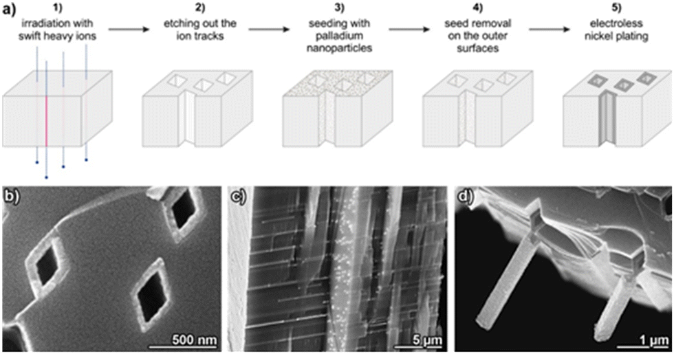 | ||
| Fig. 1 (a) Scheme of the nanotube fabrication process. (b–d) SEM images showing (b) embedded Ni nanotubes (top view), (c) a breaking edge of the mica template enclosing the Ni nanotubes, and (d) detailed images of the nanotubes partially detached from the mica template. | ||
First, we found that the formerly used Ag nanoparticle seeds resulted in dissatisfactory Ni deposit conformality and homogeneity, probably due to their low catalytic activity in oxidizing our employed reducing agents (hydrazine and dimethylamino borane).63 In order to favour plating deposition in the difficult to access narrow and recessed template pores, the seeds should ideally surpass the activity of the autocatalytic metal deposit,64 and thus efficiently initiate the reaction in not already Ni-covered areas. We realized efficient metallization in the template interior by switching to palladium nanoparticle seeds. Second, for depositing pure Ni, we chose hydrazine as a non-intrusive reducing agent in conjunction with nitrilotriacetic acid to stabilize the Ni(II) ions in the plating bath and prevent Ni(OH)2 precipitation. With this specific ligand,65 the otherwise commonly occurring Ni nanospike formation is suppressed,65,66 allowing us to realize compact deposits and thus regular nanotube walls. Third, as the Ni surface films on the top and bottom surfaces of the mica templates would interfere with the magnetic anisotropy measurements of the perpendicularly aligned nanotubes, the seeds on the outer template surface were mechanically removed (Fig. 1(a), step 4). Due to the extreme smoothness of the layered, crystalline mica sheets, seed removal is more efficient as compared to other template types (due to the absence of mechanically protected, recessed areas, and the possibility of mica layers chipping off with the seeds). As a result, the formation of a metal film outside the pores in the plating step can be avoided (Fig. 1(b)). Due to the excellent conformality of electroless-plating, the pores can be metallized throughout the complete template thickness, as it is evident from template cross-sections (Fig. 1(c)). At breaking edges, partially freed, self-supporting metal nanotubes can be found, showcasing the cohesion of the deposit and the accurate replication of the pore shape (Fig. 1(d)).
The Ni-based nanotube samples were prepared by applying Ni and Ni–B electroless-plating to an identical batch of track-etched muscovite mica patterned templates. The SEM characterization verified the deposit homogeneity and conformality in both cases, and the absence of a metal film on top of the template (Fig. 2). The nanotube wall thickness can be roughly estimated to take values of 45 ± 5 nm for both MNT variants. Due to the exact alignment of the ion beam orientation perpendicular to the template surface and the long-range crystalline order of the mica template, all pores throughout the template are strictly aligned among them in a parallel array, albeit randomly positioned (Fig. 2). Such a precisely defined geometry is required to translate any anisotropic property of the individual nanostructures to an integral measurement of the nanostructure collective, as the magnetic characterization discussed below.
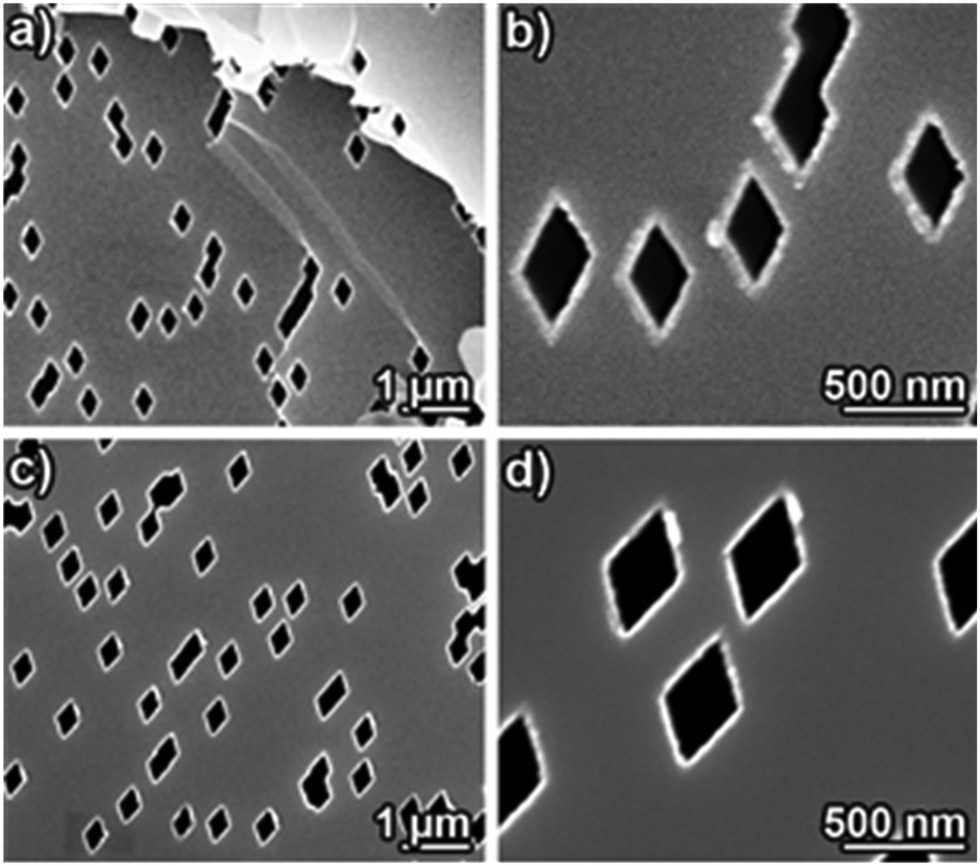 | ||
| Fig. 2 SEM top view images of track-etched muscovite mica templates with embedded rhombohedral nanotubes: (a and b) amorphous Ni–B and (c and d) nanocrystalline pure Ni. | ||
TEM was employed to gain a more detailed understanding of the MNT nanostructure. Fig. 3 shows TEM images and SAED patterns obtained in planar ultra-microtomed sections of the muscovite mica templates containing Ni–B (a, b and c) and pure Ni (d, e and f) rhombohedral nanotubes. Due to their higher mean atomic number, the dense Ni and Ni–B deposits are clearly discernible from the lighter coloured mica template, as labelled in Fig. 3(a). In the case of the Ni–B nanotube sample, the nanotube walls have a thickness of around 45 nm and are composed of grains grown from the seeds on the pore walls showing the characteristic columnar growth, which has been previously reported for the electroless deposited Ni–B and Ni–P films.67 The corresponding SAED patterns (Fig. 3(c)) display a single-crystalline diffraction pattern, which can be ascribed to the muscovite mica matrix, together with diffuse diffraction rings, the characteristic of amorphous materials, which can be associated with the Ni–B deposit. Indeed, the semi-amorphous structure of Ni–B electroless deposits has been widely reported in the literature.67,68 In contrast, the pure Ni deposits display grains of lateral dimensions of around 10 nm, which tend to aggregate leading to a densely packed film structure. The existence of multiple bright spots in the diffraction rings on the SAED spectra displayed in Fig. 3(f) suggests that the structure of the pure Ni nanotubes is nanocrystalline, which is corroborated by lively contrast fluctuations in individual grains (Fig. 3(e)).
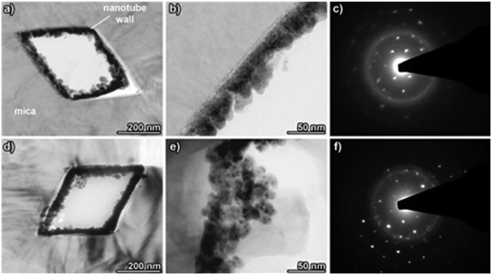 | ||
| Fig. 3 TEM images and corresponding SAED spectra of ultra-microtomed sections of track-etched muscovite mica templates with embedded rhombohedral Ni-based nanotubes: (a–c) semi-amorphous Ni–B and (d–f) nanocrystalline pure Ni. | ||
In order to confirm the conclusions regarding the crystallinity and crystallite size obtained from the TEM and SAED characterization of the Ni and Ni–B nanotubes, Ni and Ni–B powders synthesized under the same conditions as the respective nanotubes were studied by X-ray diffraction. The results are shown in Fig. 4, and strongly support the presence of the semi-amorphous phase in the Ni–B sample, as indicated by the absence of diffraction peaks in the respective pattern, which only displays two broad halos, a clear indicative of the lack of structural order. In contrast, the pure Ni sample shows broad diffraction peaks that can be indexed to the fcc Ni phase.
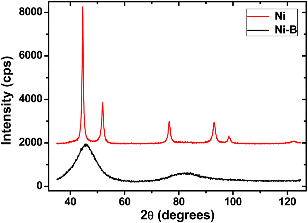 | ||
| Fig. 4 XRD diffraction patterns obtained for pure Ni (red) and boron-doped Ni (black) powders. | ||
The apparent crystallite size for this nanocrystalline phase takes values of 8 ± 2 nm according to the Le Bail fitting method.69
In order to investigate the magnetic properties of electroless deposited Ni and Ni–B alloy nanotubes, the magnetic hysteresis loops of the respective powder samples were first measured, as shown in Fig. 5. The results indicate that the semi-amorphous Ni–B alloy displays a saturation magnetization value of 0.294 emu g−1, around two orders of magnitude smaller than that of the nanocrystalline pure Ni (27.50 emu g−1). Furthermore, the coercive field of the semi-amorphous Ni–B powder takes a value of 24 Oe, whereas for pure Ni it increases up to 70 Oe.
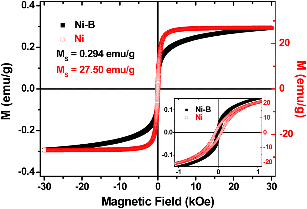 | ||
| Fig. 5 Room temperature hysteresis loops of the semi-amorphous Ni–B and nanocrystalline pure Ni powders. The inset shows an enlargement of the low-field region. | ||
The magnetic behaviour of uniformly oriented arrays of nanotubes is generally determined by the balance between different energy contributions, namely, the shape anisotropy of individual nanotubes, the magnetostatic interaction of the dipolar origin among nanotubes and the magnetocrystalline or magnetoelastic anisotropies induced in the nanotubes by the patterned templates.13,39,52 For polycrystalline Ni nanostructures synthesized and measured at room temperature, both the magnetocrystalline and magnetoelastic contributions to the effective anisotropy of the individual Ni nanotubes can be neglected. Additionally, dipolar interactions among neighbouring nanotubes in densely packed arrays, which usually competes against shape anisotropy,52,70–72 have been demonstrated to be substantially lower in nanotubes than in the equivalent nanowire systems.6,73 Therefore, due to their geometry, the length-to-diameter aspect ratio determines that the shape anisotropy, rather than the magnetocrystalline one, is expected to be the most relevant contribution to the effective anisotropy of the nanostructured system.1,9,13,74,75
The room temperature magnetic hysteresis loops measured along the three distinctive directions of the rhombohedral Ni-based nanotubes are depicted in the hysteresis loops of Fig. 6, whereas the values of the coercive field (HC) and reduced remanence (mR) for both the powder and nanotube samples are summarized in Table 1. The room temperature hysteresis loops displayed in Fig. 6(a), corresponding to Ni–B MNTs, show a nearly isotropic behavior, with low values of coercivity (2–11 Oe) and reduced remanence, mR = MR/MS, (1 – 3%) in all the three measurement directions. Despite the high aspect ratio of the Ni–B nanotubes (>40), only a slightly preferred magnetization direction along the long axis of the rhomboidal cross-section can be detected, suggesting that Ni–B nanotubes behave at room temperature as ensembles of weakly interacting quasi-superparamagnetic nanoparticles. This observation can be ascribed to the columnar structure and low saturation magnetization observed in boron-doped nickel deposits. In contrast, the hysteresis loops measured for the nanocrystalline pure Ni nanotubes (Fig. 6(b)) exhibit larger values of coercivity and reduced remanence (19–36 Oe and 8–18%, respectively). A clearly defined triaxial anisotropic behavior, consistent with the predominant contribution of shape anisotropy, is found in this sample. Therefore, the easy magnetization axis lies parallel to the pure Ni nanotube longitudinal direction (PAR). The short axis of the rhomboidal cross-section of the pure Ni nanotubes (PERP 90°) represents the hard magnetization axis of the nanotubes, whereas the long axis of the rhombohedra (PERP 0°) constitutes an intermediate magnetization direction. It is worth noting that despite the average particle size in nanocrystalline Ni deposits takes values of around 10 nm, thus being substantially smaller than the critical size for superparamagnetic transition,76 the nanotubes show well-defined ferromagnetic behaviour dominated by shape anisotropy. This fact evidences the high quality and compactness of nanocrystalline pure Ni electroless deposits. The unique 3-fold magnetic anisotropy observed in our rhomboidal nanotubes entails an additional freedom degree for tailoring the complex magnetic response of this nanostructured system, thus opening the door for novel applications in emerging fields such as in subwavelength waveguiding,54,57 magnetocalorics,77,78 drug delivery,79–81 and three-dimensional nanomagnetism.7,8,25–34,47,82
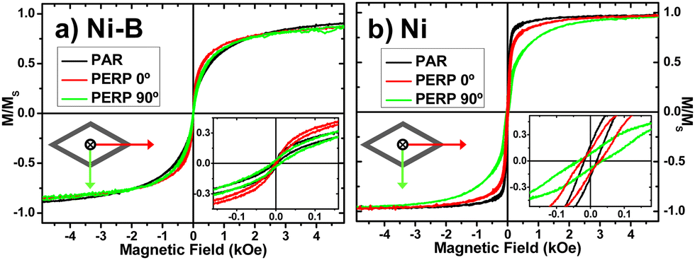 | ||
| Fig. 6 Room temperature normalized hysteresis loops of rhombohedral nanotubes for (a) amorphous Ni–B and (b) nanocrystalline pure Ni. The measurements were performed along the direction parallel to the nanotube long axis (PAR), and along the long (PERP 0°) and short (PERP 90°) axes of the rhomboidal cross-section of the nanotubes, as schematically shown in the graphs. The insets show the enlargement of the low-field regions. | ||
| Direction Sample | H C (Oe) | m R (%) | ||||
|---|---|---|---|---|---|---|
| PAR | PERP 0° | PERP 90° | PAR | PERP 0° | PERP 90° | |
| Ni–B NT | 3 | 2 | 11 | 1.5 | 1.3 | 3.3 |
| Ni–B powder | 24 | — | — | 8 | — | — |
| Ni NT | 19 | 25 | 36 | 17.9 | 12.7 | 8.1 |
| Ni powder | 73 | — | — | 14 | — | — |
Micromagnetic simulations of Ni-based MNTs
In order to qualitatively understand the origin of the magnetic response of the rhombic Ni-based nanotubes, we have performed a numerical micromagnetic model of 5 micron long amorphous Ni–B and nanocrystalline pure Ni nanotubes having a rhombic base with dimensions close to that displayed in the experimental SEM micrography reports (major and minor diagonals of 590 and 360 nm, respectively, and a wall thickness of 44 nm). It is worth mentioning that micromagnetic simulations are performed at 0 K and in single nanowires, and therefore the obtained hysteresis loops are not quantitatively comparable to the experimental measurements, but they are intended to give the qualitative explanation of the magnetization reversal processes taking place in the nanotube samples.Magnetization reversal in Ni–B MNTs
Stoichiometric measurements of the electroless deposited amorphous Ni–B powder solution reveal 25–26% of the B content for which the amorphous Ni–B bulk alloy with >25 at% B exhibits a quasi-paramagnetic behavior,83 emerging from the matrix of majority non-magnetic atoms that typically consist of the segregation of a predominant non-magnetic Ni2B phase and a diluted Ni phase.83,84 In order to test the quasi-superparamagnetic diluted phase of Ni–B alloys, our micromagnetic model of Ni–B nanotubes, performed with the finite difference discretization software mumax3,85–87 assumes a 3D Voronoi granular distribution filling approximately 1.3% volume of the nanotube with Ni grains having a mean size of 10 nm, embedded in a non-magnetic phase. We have used typical parameters of nickel as an exchange stiffness of 9 × 10⁻¹² J m−1,88 coupled with the experimental spontaneous magnetization value measured from Ni powders is 2.45 × 10⁵ A m−1. More details can be found in the ESI.†The simulated hysteresis loops (HLs) depicted in Fig. 7 confirm that the magnetization process of individual Ni–B nanotubes is nearly isotropic irrespective of the direction of the static applied field, in good agreement with experimental measurements, indicating an almost vanishing magnetostatic dipolar interaction between magnetic grains and hence among the nanotubes in the mica template. The magnetization reversal process in the Ni–B nanotube occurs through the coherent rotation of the magnetization in each grain. As the magnetic field is reduced from saturation magnetization in Fig. 7(a and b), the competition between different energies (see the ESI†) confirms that the magnetic moments in each grain rotate coherently towards its easy magnetization axis, which is uniquely determined by its low shape anisotropy. Here, we have coloured the top view with the geometry in grey colour and a standard scale to facilitate the visualization. As the field becomes gradually more negative, the magnetization begins to reverse in most of the grains of the matrix (in Fig. 7(c and d)). The reversal process concludes with the switching of the magnetization of the last few grains that remained magnetized in the initial positions at arbitrary directions as indicated in Fig. 7(e and f). More precisely, the coercivity is determined by different switching fields corresponding to each Ni grain embedded in the matrix and therefore, the quasi- superparamagnetic behaviour of the diluted magnetic phase can be observed. Strikingly, we have observed a low axial stray field in the direction of the longitudinal axis of these Ni–B nanotubes.
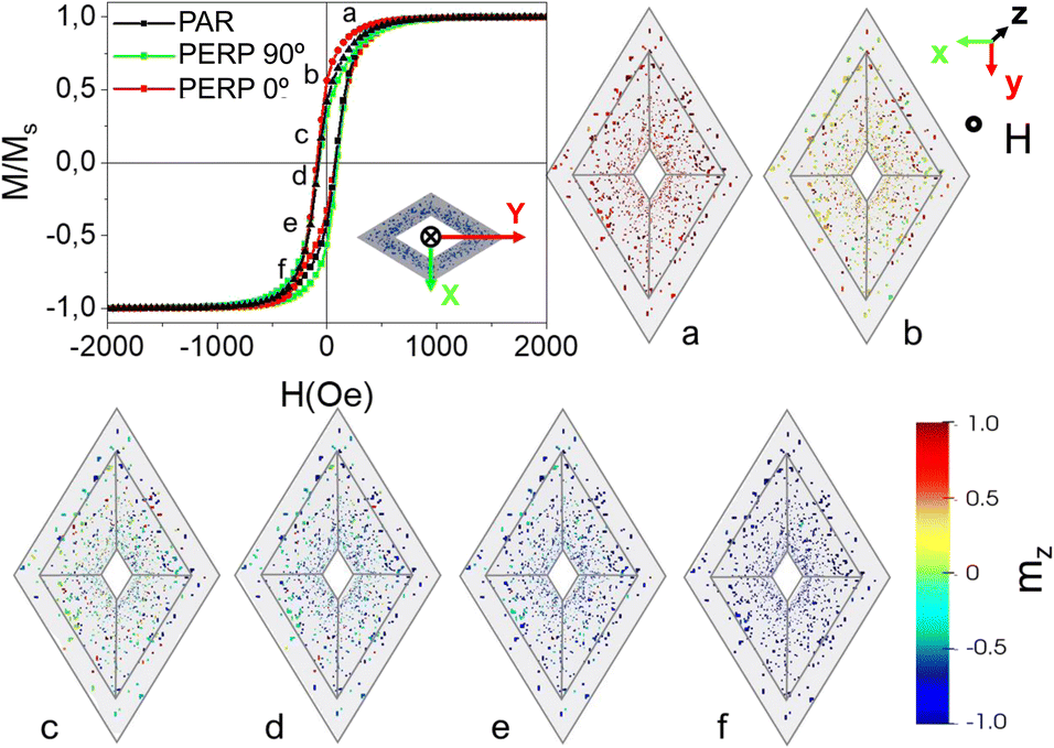 | ||
| Fig. 7 Micromagnetic modelling of the hysteresis loops for an individual Ni–B nanotube with 5 microns length, for the magnetic field applied parallel to the direction of the nanotube axis (PAR), and along the diagonals of the rhombohedral basis (PERP 0° and 90°), respectively. (a–f). Top views of the nanotube during the magnetization reversal process with an applied field in the direction parallel to the nanotube length (axial direction) The magnetic grains have been colored according to the axial component of magnetization, mz. | ||
Overall, the isotropic magnetic response of the rhombic matrix with a low net magnetic moment, low axial stray fields and an anhysteretic coherent response coupled with the hollow geometry provide appealing features for bioapplications such as the encapsulation of magnetic nanoparticles for drug delivery as well as in magnetic nanocarriers directionally oriented under weak applied magnetic fields with low amplitude values.
Magnetization reversal in Ni MNTs
Regarding the magnetization reversal process in individual polycrystalline pure Ni nanotube with an identical morphology, micromagnetic modelling has enlighten a rich variety of reversal modes with an applied magnetic field. The hysteresis loops displayed in Fig. 8(a) were simulated using the mumax3 system and typical parameters of Ni (see the ESI†), and showed a qualitatively similar behaviour to that experimentally measured in pure Ni MNTs.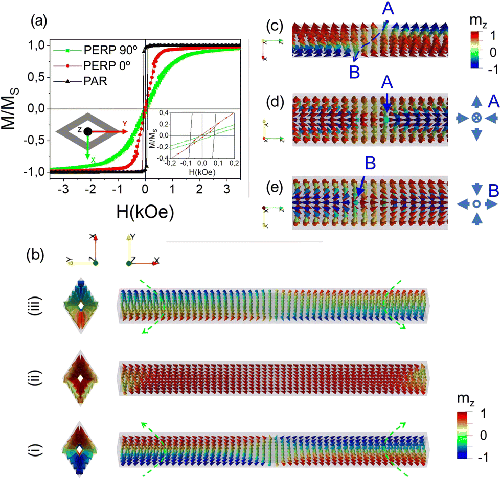 | ||
| Fig. 8 (a) Micromagnetic simulations of the magnetic hysteresis loops corresponding to the three directions of the applied field for an individual nanocrystalline pure Ni rhombic nanotube, namely the axial (PAR), together mayor (PERP 0°) and minor (PERP 90°) diagonals of the rhombic nanotube, respectively. (b) Top and lateral views of the magnetic configuration in the Ni rhombic nanotube showing the collapse of two onion states colliding on an antivortex state or a transversal magnetic domain wall. | ||
The squared hysteresis loop obtained with the magnetic field applied parallel to the axis of the rhombic Ni nanotube (HL in black color) indicates a bistable magnetic behavior dominated by the shape anisotropy. The magnetization reversal takes place through vortex domain wall nucleation at the end of the rhombic Ni nanotube, depinning and subsequent propagation towards the opposite end of the nanotube (see the ESI†).
Turning now to the hysteresis loop when the magnetic field is applied along the mayor diagonal (PERP 0°) of the nanotube, the model reveals a complex magnetization reversal process, which proceeds through the formation of onion-like at the ends of the nanotubes depicted in Fig. 8(b)(i–iii) that form three-dimensional topologically nontrivial magnetic configuration states.89,90 An important remark is the resemblance of the closure domains with C-states typically formed in rectangular planar magnetic layers that evince a hard magnetization axis in this direction. The shape anisotropy and the main role of the demagnetization field for these directions govern the complex magnetization reversal process along the two diagonals of the rhombic Ni nanotube.
Concerning the hysteresis loop for the magnetic field applied along the minor diagonal of the rhombic nanotube (PERP 90°) we observed the lowest remanence of the three directions, but higher coercivity values than in the case of the HL along the mayor diagonal as corresponds to the hardest direction. Here the reversal mechanism starts with the nucleation of onion-like closure domains (see the ESI†). A small increase in the PERP 90° HL around a field value of 500 Oe reveals the formation of an asymmetric magnetic state depicted in Fig. 8(c–e) formed by a vortex–antivortex structure on the surface of the wire. While, on average, VSM measurements on the patterned templates of nanotubes mask the formation of these states, micromagnetic modeling confirms a diversity of reversal modes emerging from the geometrical frustration of the rhombic geometry coupled with the hollow morphology.
Conclusions
Ni-based magnetic nanotubes with rhombohedral cross-section and a wall thickness of around ∼45 nm have been successfully deposited onto track-etched mica templates using an optimized electroless-plating method, employing semi-amorphous B-doped Ni and nanocrystalline pure Ni as the constituent nanotube material. Our high deposit quality, characterized by an excellent fidelity of the pore shape replica and strong deposit cohesion, in conjunction with the simplicity, speed and flexibility of the solely wet-chemical method corroborates the high suitability of electroless-plating for the template-assisted fabrication of magnetic nanomaterials, paving the path towards complex nanotube constitutions and architectures through the careful control of the composition, nanostructure and 3D arrangement of the 1D nanoscale building blocks.The magneto-structural characterization of the Ni–B nanotubes points out to their low magnetic remanence and coercivity, which are due to the semi-amorphous structure and the boron content that results in low saturation magnetization and nearly negligible magnetic shape anisotropy for these nanotubes. In contrast, rhomboidal nanotubes composed of nanocrystalline Ni display enhanced magnetic behavior in terms of both remanence and shape anisotropy. Remarkably, the rhombohedral geometry of the Ni nanotubes is directly reflected in the triaxial magnetic anisotropy. Compared to conventional cylindrical nanowire or nanotube arrays, this novel geometry provides an additional degree of freedom for tuning the particular magnetic behavior exhibited by these nanostructures and their magnetic state at remanence, further limiting the magnetic domain reversal due to the sharp edge angles at the nanotube corners, which can lead to the appearance of magnetic singularities near the nanotube vertex inducing the nucleation of magnetic domain walls. The future of such peculiar nanotube geometries by varying their compositions and size properties could lead to interesting novel magnetic phenomena related to their magnetic domain wall movements, with applications in the fields of electronics or computing, as well as in biomedicine or catalysis.
Author contributions
Conceptualization and methodology: W. E., J. G., J. A. F. R., and V. M. P. Investigation: S. S., F. M., A. S. G. G., M. M., U. K. and V. V. Resources and funding acquisition: W. E. and V. M. P. Formal analysis: J. G., J. A. F. R., V. V., F. M., and U. K. Supervision: V. M. P. Visualization: F. M., V. V., and M. M. Writing: all authors have contributed to the preparation of the manuscript in its final form.Conflicts of interest
There are no conflicts to declare.Acknowledgements
We thank Prof. Dr Christina Trautmann and the Materials Research Division of the GSI Helmholtz Centre for Heavy Ion Research (Darmstadt, Germany) for irradiating the muscovite mica sheets. The results presented here are based on the UMAT experiment, which was performed at the X0-beamline of the UNILAC at the GSI Helmholtzzentrum für Schwerionenforschung, Darmstadt (Germany) in the frame of FAIR Phase-0. Spanish Ministery of Science and Innovation (MICINN) and Research State Agency (AEI), under grant PID2019-108075RB-C32, are acknowledged. Scientific support of common research services of SCTs from Universidad de Oviedo is also gratefully recognized.References
- A. Kumar, S. Fähler, H. Schlörb, K. Leistner and L. Schultz, Phys. Rev. B: Condens. Matter Mater. Phys., 2006, 73, 064421, DOI:10.1103/PhysRevB.73.064421.
- J. F. Rohan, D. P. Casey, B. M. Ahern, F. M. F. Rhen, S. Roy, D. Fleming and S. E. Lawrence, Electrochem. Commun., 2008, 10, 1419, DOI:10.1016/j.elecom.2008.07.019.
- X. F. Han, S. Shamaila, R. Sharif, J. Y. Chen, H. R. Liu and D. P. Liu, Adv. Mater., 2009, 21, 4619, DOI:10.1002/adma.200901065.
- K. Pitzschel, J. M. Montero-Moreno, J. Escrig, O. Albrecht, K. Nielsch and J. Bachmann, ACS Nano, 2009, 3, 3463, DOI:10.1021/nn900909q.
- D. P. Weber, D. Rüffer, A. Buchter, F. Xue, E. Russo-Averchi, R. Huber, P. Berberich, J. Arbiol, A. Fontcuberta i Morral, D. Grundler and M. Poggio, Nano Lett., 2012, 12, 6139, DOI:10.1021/nl302950u.
- M. P. Proença, C. T. Sousa, J. Escrig, J. Ventura, M. Vázquez and J. P. Araujo, J. Appl. Phys., 2013, 113, 093907, DOI:10.1063/1.4794335.
- E. Araujo, A. Encinas, Y. Velázquez-Galván, J. M. Martínez-Huerta, G. Hamoir, E. Ferain and L. Piraux, Nanoscale, 2015, 7, 1485, 10.1039/C4NR04800H.
- A. Fernández-Pacheco, R. Streubel, O. Fruchart, R. Hertel, P. Fischer and R. P. Cowburn, Nat. Commun., 2017, 8, 15756, DOI:10.1038/ncomms15756.
- Y. Veláquez-Galván, J. de la Torre Medina, L. Piraux and A. Encinas, J. Magnetism Magnetic Mater., 2020, 497, 165992, DOI:10.1016/j.jmmm.2019.165992.
- V. Raposo, J. M. Garcia, J. M. González and M. Vázquez, J. Magnetism Magnetic Mater., 2000, 222, 227, DOI:10.1016/S0304-8853(00)00563-1.
- Q. F. Zhan, J. H. Gao, Y. Q. Liang, N. L. Di and Z. H. Cheng, Phys. Rev. B: Condens. Matter Mater. Phys., 2005, 72, 024428, DOI:10.1103/PhysRevB.72.024428.
- M. Pardavi-Horvath, P. E. Si, M. Vazquez, W. O. Rosa and G. Badini, J. Appl. Phys., 2008, 103, 07D517, DOI:10.1063/1.2833304.
- H. Schlörb, V. Haehnel, M. S. Khatri, A. Srivastav, A. Kumar, L. Schultz and S. Fähler, Phys. Status Solidi B, 2010, 247, 2364, DOI:10.1002/pssb.201046189.
- V. M. Prida, J. García, B. Hernando, C. Bran, L. G. Vivas and M. Vázquez, Electrochemical synthesis of magnetic nanowires with controlled geometry and magnetic anisotropy, Magnetic Nano- and Microwires, Woodhead Publishing, 2015, pp. 41–104 DOI:10.1016/B978-0-08-100164-6.00002-3.
- S. J. Son, J. Reichel, B. He, M. Schuchman and S. B. Lee, J. Am. Chem. Soc., 2005, 127, 7316, DOI:10.1021/ja0517365.
- R. Zierold, Z. Wu, J. Biskupek, U. Kaiser, J. Bachmann, C. E. Krill III and K. Nieslch, Adv. Funct. Mater., 2011, 21, 226, DOI:10.1002/adfm.201001395.
- P. Landeros, S. Allende, J. Escrig, E. Salcedo and D. Altbir, Appl. Phys. Lett., 2007, 90, 102501, DOI:10.1063/1.2437655.
- S. Allende, J. Escrig, D. Altbir, E. Salcedo and M. Bahiana, Eur. Phys. J. B, 2008, 66, 37, DOI:10.1140/epjb/e2008-00385-4.
- J. Escrig, J. Bachmann, J. Jing, M. Daub, D. Altbir and K. Nielsch, Phys. Rev. B: Condens. Matter Mater. Phys., 2008, 77, 214421, DOI:10.1103/PhysRevB.77.214421.
- J. Bachmann, J. Escrig, K. Pitzschel, J. M. Montero Moreno, J. Jing, D. Görlitz, D. Altbir and K. Nielsch, J. Appl. Phys., 2009, 105, 07B521, DOI:10.1063/1.3074109.
- O. Albrecht, R. Zierold, S. Allende, J. Escrig, C. Patzig, B. Rauschenbach, K. Nielsch and D. Görlitz, J. Appl. Phys., 2011, 109, 093910, DOI:10.1063/1.3583666.
- M. P. Proença, C. T. Sous, J. Ventura, J. P. Araujo, J. Escrig and M. Vázquez, Spin, 2012, 2, 1250014, DOI:10.1142/S2010324712500142.
- D. Richardson, S. Kingston and F. M. F. Rhen, AIP Adv., 2016, 6, 056113, DOI:10.1063/1.4943603.
- M. Staňo, S. Schaefer, A. Wartelle, M. Rioult, R. Belkhou, A. Sala, T. Onur Menteş, A. Locatelli, L. Cagnon, B. Trapp, S. Bochmann, S. Martin, E. Gautier, J. C. Toussaint, W. Ensinger and O. Fruchart, SciPost Phys., 2018, 5, 038, DOI:10.21468/SciPostPhys.5.4.038.
- P. Fischer, D. Sanz-Hernández, R. Streubel and A. Fernández-Pacheco, APL Mater., 2020, 8, 010701, DOI:10.1063/1.5134474.
- J. A. Otárola, M. Yan, H. Schultheiss, R. Hertel and A. Kákay, Phys. Rev. Lett., 2016, 117, 227203, DOI:10.1103/PhysRevLett.117.227203.
- E. C. Burks, D. A. Gilbert, P. D. Murray, C. Flores, T. E. Felter, S. Charnvanichborikarn, S. O. Kucheyev, J. D. Colvin, G. Yin and K. Liu, Nano Lett., 2021, 21, 716–722, DOI:10.1021/acs.nanolett.0c04366.
- M. Yan, C. Andreas, A. Kákay, F. García-Sánchez and R. Hertel, Appl. Phys. Lett., 2011, 99, 122505, DOI:10.1063/1.3643037.
- M. M. Salazar-Cardona, L. Körber, H. Schultheiss, K. Lenz, A. Thomas, K. Nielsch, A. Kákay and J. A. Otálora, Appl. Phys. Lett., 2021, 118, 262411, DOI:10.1063/5.0048692.
- M. C. Giordano, K. Baumgaertl, S. Escobar Steinvall, J. Gay, M. Vuichard, A. Fontcuberta i Morral and D. Grundler, ACS Appl. Mater. Interfaces, 2020, 12, 40443–40452, DOI:10.1021/acsami.0c06879.
- M. C. Giordano, S. Escobar Steinvall, S. Watanabe, A. Fontcuberta i Morral and D. Grundler, Nanoscale, 2021, 13, 13451–13462, 10.1039/D1NR02291A.
- B. Hussain and M. G. Cottam, J. Magn. Magn. Mater., 2021, 539, 168344, DOI:10.1016/j.jmmm.2021.168344.
- J. A. Otálora, M. Yan, H. Schultheiss, R. Hertel and A. Kákay, Phys. Rev. B, 2017, 95, 184415, DOI:10.1103/PhysRevB.95.184415.
- J. Yang, J. Kim, B. Kim, Y. J. Cho, J. H. Lee and S. K. Kim, J. Appl. Phys., 2018, 123, 033901, DOI:10.1063/1.5010405.
- F. Muench, E. M. Felix, M. Rauber, S. Schaefer, M. Antoni, U. Kunz, H. J. Kleebe, C. Trautmann and W. Ensinger, Electrochim. Acta, 2016, 202, 47, DOI:10.1016/j.electacta.2016.03.188.
- M. P. Proença, C. T. Sousa, J. Ventura, M. Vazquez and J. P. Araujo, Nanoscale Res. Lett., 2012, 7, 280, DOI:10.1186/1556-276X-7-280.
- J. A. Fernandez-Roldan, D. Chrischon, L. S. Dorneles, O. Chubykalo-Fesenko, M. Vazquez and C. Bran, Nanomaterials, 2018, 8, 692, DOI:10.3390/nano8090692.
- K. Pitzschel, J. Bachmann, J. M. Montero-Moreno, J. Escrig, D. Görlitz and K. Nielsch, Nanotechnology, 2012, 23, 495718, DOI:10.1088/0957-4484/23/49/495718.
- A. Pereira, J. L. Palma, J. C. Denardin and J. Escrig, Nanotechnology, 2016, 27, 345709, DOI:10.1088/0957-4484/27/34/345709.
- W. Wang, N. Li, X. Li, W. Geng and S. Qiu, Mater. Res. Bull., 2006, 41, 1417, DOI:10.1016/j.materresbull.2006.02.011.
- S. Schaefer, E. M. Felix, F. Muench, M. Antoni, C. Lohaus, J. Brötz, U. Kunz, I. Gärtner and W. Ensinger, RSC Adv., 2016, 74, 70033, 10.1039/C6RA10235B.
- J. Sudagar, J. Lian and W. Sha, J. Alloys Compds., 2013, 571, 183, DOI:10.1016/j.jallcom.2013.03.107.
- D. Gong, J. Cai, N. Celi, L. Feng, Y. Jiang and D. Zhang, J. Magnetism Magnetic Mater., 2016, 468, 148, DOI:10.1016/j.jmmm.2018.08.001.
- F. Muench, L. Sun, T. Kottakkat, M. Antoni, S. Schaefer, U. Kunz, L. Molina-Luna, M. Duerrschnabel, H. J. Kleebe, S. Ayata, C. Roth and W. Ensinger, ACS Appl. Mater. Interfaces, 2017, 9, 771, DOI:10.1021/acsami.6b13979.
- F. Muench, U. Kunz, H. F. Wardenga, H. J. Kleebe and W. Ensinger, Langmuir, 2014, 30, 10878, DOI:10.1021/la5012956.
- Y. T. Chong, D. Görlitz, S. Martens, M. Y. E. Yau, S. Allende, J. Bachmann and K. Nielsch, Adv. Mater., 2010, 22, 2435, DOI:10.1002/adma.200904321.
- J. de la Torre Medina, T. da Câmara Santa Clara Gomes, Y. G. Velázquez Galván and L. Piraux, Sci. Rep., 2018, 8, 14555, DOI:10.1038/s41598-018-32437-8.
- M. E. Toimil-Molares, Beilstein J. Nanotechnol., 2012, 3, 860–883, DOI:10.3762/bjnano.3.97.
- C. Trautmann, Micro- and Nanoengineering with Ion Tracks, Ion Beams in Nanoscience and Technology. Particle Acceleration and Detection, Springer, Berlin, Heidelberg, 2009, pp. 369–387. DOI:10.1007/978-3-642-00623-4_30.
- E. Kaniukov, A. Shumskaya, A. Kozlovskiy, M. Zdorovets, A. Trukhanov, T. Zubar, D. Tishkevich, D. Vinnik, D. R. Khairetdinova, S. Evstigneeva, V. S. Rusakov, B. Rameev and L. Panina, Structure and magnetic properties of FeCo nanotubes obtained in pores of ion track templates, Nano-Struct. Nano-Objects, 2021, 26, 100691, DOI:10.1016/j.nanoso.2021.100691.
- M. Staňo, S. Schaefer, A. Wartelle, M. Rioult, R. Belkhou, A. Sala, T. O. Menteş, A. Locatelli, L. Cagnon, B. Trapp, S. Bochmann, S. Y. Martin, E. Gautier, J. C. Toussaint, W. Ensinger and O. Fruchart, SciPost Phys., 2018, 5, 038, DOI:10.21468/SciPostPhys.5.4.038.
- V. Vega, T. Böhnert, S. Martens, M. Waleczek, J. M. Montero-Moreno, D. Görlitz, V. M. Prida and K. Nielsch, Nanotechnology, 2012, 23, 465709, DOI:10.1088/0957-4484/23/46/465709.
- B. Paivanranta, H. Merbold, R. Giannini, L. Buchi, S. Gorelick, C. David, J. F. Loffler, T. Feurer and Y. Ekinci, ACS Nano, 2011, 5, 6374, DOI:10.1021/nn201529x.
- D. Mo, J. Liu, J. Duan, H. Yao, Y. Chen, Y. Sun and P. Zhai, Mater. Lett., 2012, 68, 201, DOI:10.1016/j.matlet.2011.10.033.
- R. V. Goldstein, V. A. Gorodtsov and D. S. Lisovenko, Dokl. Phys., 2013, 58, 400, DOI:10.1134/S1028335813090097.
- T. Yanagishita, M. Sasaki, K. Nishio and H. Masuda, Adv. Mater., 2004, 16, 429, DOI:10.1002/adma.200306012.
- A. K. Jitender, Optics Commun., 2017, 382, 337, DOI:10.1016/j.optcom.2016.08.011.
- C. F. Tan, A. K. S. S. Zin, Z. Chen, C. H. Liow, H. T. Phan, H. R. Tan, Q. H. Xu and G. W. Ho, ACS Nano, 2018, 12, 4512, DOI:10.1021/acsnano.8b00770.
- L. Sun, L. Chien and P. C. Searson, J. Mater. Sci., 2000, 35, 1097, DOI:10.1023/A:1004703529210.
- L. Sun, P. C. Searson and C. L. Chien, Appl. Phys. Lett., 1999, 74, 2803–2805, DOI:10.1063/1.124019.
- A. M. Bratkovsky, S. N. Rashkeev, A. V. Smirnov and G. Wendin, Europhys. Lett., 1994, 26, 43, DOI:10.1209/0295-5075/26/1/008.
- F. Muench, G. A. El-Nagar, T. Tichter, A. Zintler, U. Kunz, L. Molina-Luna, V. Sikolenko, C. Pasquini, I. Lauermann and C. Roth, ACS Appl. Mater. Interfaces, 2019, 11, 43081, DOI:10.1021/acsami.9b12783.
- I. Ohno, O. Wakabayashi and S. Haruyama, J. Electrochem. Soc., 1985, 132, 2323, DOI:10.1149/1.2113572.
- F. Muench, A. Eils, M. E. Toimil-Molares, U. H. Hossain, A. Radetinac, C. Stegmann, U. Kunz, S. Lauterbach, H. J. Kleebe and W. Ensinger, Surf. Coat. Technol., 2014, 242, 100, DOI:10.1016/j.surfcoat.2014.01.024.
- T. Boettcher, S. Schaefer, M. Antoni, T. Stohr, U. Kunz, M. Duerrschnabel, L. Molina-Luna, W. Ensinger and F. Muench, Langmuir, 2019, 35, 4246, DOI:10.1021/acs.langmuir.9b00030.
- L. Chen, H. Liu, L. Liu, Y. Zheng, H. Tang and Z. Liu, Crystals, 2018, 8, 397, DOI:10.3390/cryst8110397.
- A. Mukhopadhyay, T. K. Barman and P. Sahoo, Proc. Inst. Mech. Eng. L, 2020, 235, 149–161, DOI:10.1177/1464420720956270.
- Electroless Plating: Fundamentals and Applications, Ch. 4 “The Properpies of Electroless Nickel, ed. G. O. Mallory and J. B. Hajdu, William Andrew Publishing, 1990, ISBN: 978-0-936569-07-9 Search PubMed.
- A. Le Bail, Powder Diffr., 2005, 20, 316, DOI:10.1154/1.2135315.
- J. De La Torre-Medina, M. Darques, L. Piraux and A. Encinas, J. Appl. Phys., 2009, 105, 023909, DOI:10.1063/1.3067773.
- F. Zighem, T. Maurer, F. Ott and G. Chaboussant, J. Appl. Phys., 2011, 109, 013910, DOI:10.1063/1.3518498.
- J. M. Martínez-Huerta, J. De La Torre Medina, L. Piraux and A. Encinas, J. Appl. Phys., 2012, 111, 083914, DOI:10.1063/1.4704397.
- Y. Velázquez-Galván, J. M. Martínez-Huerta, J. De la Torre Medina, Y. Danlée, L. Piraux and A. Encinas, J. Phys.: Condens. Matter, 2014, 26, 026001, DOI:10.1088/0953-8984/26/2/026001.
- D. Navas, K. Pirota, P. Mendoza Zelis, D. Velazquez, C. A. Ross and M. Vazquez, J. Appl. Phys., 2008, 103, 07D523, DOI:10.1063/1.2834719.
- N. Han, G. Guo, L. Zhang, G. Zhang and W. Song, J. Mater. Sci. Technol., 2009, 25, 151–154 CAS . https://www.jmst.org/EN/Y2009/V25/I02/151.
- S. Singamaneni, V. N. Bliznyuk, C. Binek and E. Y. Tsymbal, J. Mater. Chem., 2011, 21, 16819, 10.1039/C1JM11845E.
- V. Franco, K. R. Pirota, V. M. Prida, A. M. J. C. Neto, A. Conde, M. Knobel, B. Hernando and M. Vazquez, Phys. Rev. B: Condens. Matter Mater. Phys., 2008, 77, 104434, DOI:10.1103/PhysRevB.77.104434.
- D. Serantes, V. Vega, W. O. Rosa, V. M. Prida, B. Hernando, M. Pereiro and D. Baldomir, Phys. Rev. B: Condens. Matter Mater. Phys., 2012, 86, 104431, DOI:10.1103/PhysRevB.86.104431.
- M. Hammad Aziz, M. Fakhar-e-Alam, M. Fatima, F. Shaheen, S. Iqbal, M. Atif, M. Talha, S. Mansoor Ali, M. Afzal, A. Majid, T. Shelih Al Harbi, M. Ismail, Z. M. Wang, M. S. AlSalhi and Z. A. Alahmed, PLoS One, 2016, 11, e0150295, DOI:10.1371/journal.pone.0150295.
- A. L. Kozlovskiy, I. V. Korolkov, G. Kalkabay, M. A. Ibragimova, A. D. Ibrayeva, M. V. Zdorovets, V. S. Mikulich, D. V. Yakimchuk, A. E. Shumskaya and E. Yu. Kaniukov, J. Nanomater., 2017, 2017, 3060972, DOI:10.1155/2017/3060972.
- A. Kozlovskiy, M. Zdorovets, K. Kadyrzhanov, I. Korolkov, V. Rusakov, L. Nikolaevich, O. Fesenko, O. Budnyk, D. Yakimchuk, A. Shumskaya and E. Kaniukov, Appl. Nanosci., 2019, 9, 1091–1099, DOI:10.1007/s13204-018-0889-3.
- D. D. Sheka, Appl. Phys. Lett., 2021, 118, 230502, DOI:10.1063/5.0048891.
- K. I. Portnoi, V. M. Romashov, V. M. Chubarov, M. K. Levinskaya and S. E. Salibekov, Sov. Powder Metall. Met. Ceram., 1967, 6, 99, DOI:10.1007/BF00775639.
- I. Bakonyi, E. Babić, M. Miljak, R. Lück, J. Bahle, R. Hasegawa and J. Kollár, Phys. Rev. B: Condens. Matter Mater. Phys., 2002, 65, 104423, DOI:10.1103/PhysRevB.65.104423.
- A. Vansteenkiste, J. Leliaert, M. Dvornik, M. Helsen, F. Garcia-Sanchez and B. V. Waeyenberge, AIP Adv., 2014, 4, 107133, DOI:10.1063/1.4899186.
- L. Exl, S. Bance, F. Reichel, T. Schrefl, H. P. Stimming and N. J. Mauser, J. Appl. Phys., 2014, 115, 17D118, DOI:10.1063/1.4862839.
- J. Leliaert, B. Van de Wiele, A. Vansteenkiste, L. Laurson, G. Durin, L. Dupré and B. Van Waeyenberge, J. Appl. Phys., 2014, 115, 233903, DOI:10.1063/1.4883297.
- C. I. L. de Araujo, R. C. Silva, I. R. B. Ribeiro, F. S. Nascimento, J. F. Felix, S. O. Ferreira, L. A. S. Mól, W. A. Moura-Melo and A. R. Pereira, Appl. Phys. Lett., 2014, 104, 092402, DOI:10.1063/1.4867530.
- C. Mu, J. Song, J. Xu and F. Wen, AIP Adv., 2016, 6, 065026, DOI:10.1063/1.4955156.
- J. A. Fernandez-Roldan, D. Chrischon, L. S. Dorneles, O. Chubykalo-Fesenko, M. Vazquez and C. Bran, Nanomaterials, 2018, 8, 692, DOI:10.3390/nano8090692.
Footnote |
| † Electronic supplementary information (ESI) available. See DOI: https://doi.org/10.1039/d3tc00857f |
| This journal is © The Royal Society of Chemistry 2023 |