
 Open Access Article
 This Open Access Article is licensed under a
 Creative Commons Attribution 3.0 Unported Licence
Influence of the defect density on the ordering of an NHC monolayer on a silicon surface†
Robert
Zielinski
 a,
Mowpriya
Das
b,
Canan
Kosbab
a,
Mike Thomas
Nehring
a,
Mario
Dähne
a,
Norbert
Esser
*ac,
Martin
Franz
*a and
Frank
Glorius
*b
a,
Mowpriya
Das
b,
Canan
Kosbab
a,
Mike Thomas
Nehring
a,
Mario
Dähne
a,
Norbert
Esser
*ac,
Martin
Franz
*a and
Frank
Glorius
*b
aTechnische Universität Berlin, Institut für Festkörperphysik, Hardenbergstrasse 36, 10623 Berlin, Germany. E-mail: martin.franz@physik.tu-berlin.de
bWestfälische Wilhelms-Universität Münster, Organisch-Chemisches Institut, Corrensstrasse 40, 48149 Münster, Germany. E-mail: glorius@uni-muenster.de
cLeibniz-Institut für Analytische Wissenschaften – ISAS e.V., Schwarzschildstrasse 8, 12489 Berlin, Germany. E-mail: norbert.esser@isas.de
First published on 27th April 2023
Abstract
Silicon is the element of choice in semiconductor devices and the functionalization of silicon surfaces is highly desirable for electronic industries. N-Heterocyclic carbenes have been demonstrated to be promising modifiers and anchors for surface functionalization, but so far mainly on metal surfaces. Here, the adsorption behavior of cyclohexyl cyclic (alkyl)(amino)carbene molecules on a silicon surface is investigated using scanning tunneling microscopy. Surprisingly and quite unexpected on semiconductors, we find a self-limited, well ordered growth of a stable monolayer with large domains. The overlayer is characterized by a 3 × 3 periodicity and an upright adsorption geometry of the molecules leading to a strong work function reduction. Moreover, we find that the surface defect density strongly influences the grade of ordering, as the initial adsorption of the molecules takes place on a defect site. Thus, in the studied material system, the defect density of the substrate directly determines the domain sizes.
Introduction
In the race towards miniaturization of electronic devices, the demand for producing structures with shrinking geometries is higher than ever. However, the currently used lithographic methods will soon reach their physical limits. Modifying semiconductor surfaces, preferably Si, with ordered adsorbed organic layers can be an alternative procedure to bypass this dead end.1,2 While the study of self-assembled monolayers on metal surfaces is well established,3–12 the preparation of well ordered stable organic films with defined properties on semiconductor surfaces is still in its infancy. The low mobility caused by the high density of reactive dangling bonds on such surfaces prevents the diffusion required for the ordering of the molecular layers.In contrast to most Si surfaces, the Si(111) R30°–B surface (Si(111)–B) features partially removed dangling bonds, making it more suitable for the ordered growth of organic films, as demonstrated in previous works.13–19 At the Si(111)–B surface, schematically shown in Fig. 1(a and b), every third Si atom in the 2nd layer is replaced by a B atom, leading to an electron transfer from the Si adatoms to the B atoms and finally to a chemically passivated surface.20,21 A more detailed description of the surface structure can be found in the ESI† Section 3.
 | ||
| Fig. 1 Structure model of the Si(111)–B surface in (a) side view with the typical Si–Si(S5) defect and (b) top view. (c) Adsorption process of the cyCAAC molecule used in this work. | ||
Cyclic (alkyl)(amino)carbenes (CAAC) belong to the group of N-heterocyclic carbenes (NHCs), which have received substantial attention in the past.3,4,7,8,10,12,19,22–30 Their variable structure together with the strong and highly directional binding of the so-called carbene C atom to surfaces renders these NHC molecules to be perfect anchors for the target-oriented functionalization of surfaces.12,31–44 The CAAC molecules possess only one amino substituent in the ring structure, which makes them even stronger σ-donors than the imidazolylidene-based NHCs containing two amino substituents.45 Although studies investigated the self-assembly of CAAC molecules on Au(111), Ag(111), and Cu(111) surfaces,3,46 on semiconductors only H-terminated Si substrates have been investigated to date.33,47
In this work, we investigate the adsorption of cyclohexyl CAAC (cyCAAC) (see Fig. 1(c)) on the Si(111)–B surface using scanning tunneling microscopy (STM) and low-energy electron diffraction (LEED), accompanied by X-ray photoelectron spectroscopy (XPS) to determine the work function change upon the adsorption of the molecules. The cyCAAC molecules were deposited in situ as schematically shown in Fig. 1(c), using cyCAAC-CO2 adducts as precursors, as introduced earlier.3 When heated under ultra-high vacuum (UHV) conditions, CO2 is detached and a molecular beam of the free cyCAAC molecules for the deposition on the surface is obtained (see also Section 2.1 of the ESI†).
An upright adsorption (“upright” referring to the N-heterocycle plane) of the cyCAAC molecules on top of Si substrate adatoms is found. For the monolayer coverage, cyCAAC forms a highly ordered monolayer characterized by domains with a 3 × 3 periodicity. The domain size thereby strongly depends on the surface defect density of the Si(111)–B substrate that can be tuned by the concentration of B bulk doping, reaching ∼130 nm2 in the case of a low defect density. A strong work function reduction of 1.86 eV is found for the cyCAAC monolayer on the low defect density substrate comparable to the behavior of other NHCs on surfaces.19
Results and discussion
The clean surface was characterized using STM, LEED, and XPS prior to the adsorption experiments of cyCAAC molecules in order to determine the cleanliness and the defect density of the substrate. Fig. 2(a) shows a representative STM image of the Si(111)–B surface with the Si adatoms appearing as bright spots. A unit cell is indicated in the enlarged view shown as the inset. Besides the ideal surface reconstruction, also its typical point defects are visible. The majority are the so called Si–Si(S5) defects, where the Si atom under the adatom is not replaced by a B atom (see Fig. 1(a) and ESI† Section 3), appearing brighter at the used tunneling voltage.15 These defect sites are known to act as the preferred adsorption sites for molecules, as demonstrated for cobalt phthalocyanine (CoPc) and also NHCs.17,19Ab initio calculations revealed an energetic preference for NHC adsorption on these defect sites as compared to regular surface sites.19
 | ||
| Fig. 2 (a) STM image (sample voltage VS = + 2.2 V and tunneling current IT = 50 pA) of the clean Si(111)–B surface, with magnification in the inset. A unit cell and examples of the occurring point defects are indicated. (b) LEED pattern acquired at a kinetic energy of 50 eV. | ||
A point defect with a missing Si adatom appears darker and is either called V–B(S5) or V–Si(S5), depending on which atom is located in the 2nd layer (see Section 3 of the ESI†). Fig. 2(b) shows the LEED pattern of the surface. The 1 × 1 unit cell of the unreconstructed surface and the  unit cell of the Si(111)–B surface, which is rotated by 30°, are indicated.
After the deposition of a low coverage of cyCAAC molecules on this surface, single bright, round shaped spots appear in the STM images, as shown in Fig. 3(a and b), which are assigned to the cyCAAC molecules adsorbed on the surface. The clean surface with its  R30° reconstruction is still visible in between these brighter spots. As no diffusion of adsorbed molecules is observed when the same area is imaged repeatedly, a stable adsorption is concluded. Only occasionally tip-induced movements are observed, as indicated in Fig. 3(a) by a circle, where an initially imaged molecule suddenly disappears at the next higher scan line.
 | ||
| Fig. 3 (a and b) STM images with a submonolayer coverage (VS = +2.4 V, IT = 15 pA). (b) Determination of the adsorption site and (c) height profile across a single molecule as marked in (b). (d) STM image of an increased coverage (VS = +2.3 V, IT = 10 pA). | ||
In the following, we demonstrate that the molecules adsorb in a similar geometry as found for the previously investigated NHCs.19 Thereby, the carbene C atom forms a highly directional covalent bond to the Si adatom of the Si(111)–B substrate leading to an upright orientation of the heterocyclic ring (referred to as upright adsorption in the following). To prove that cyCAAC also binds to Si adatoms, lines along the adatoms in each of the three main directions are indicated in Fig. 3(b), revealing the location of the adsorbed molecule directly on top of the Si adatom. The upright orientation of the inner NHC ring is now concluded on the basis of height profiles such as the one shown in Fig. 3(c). The measured apparent height of 0.32 nm is considerably lower as compared to the geometric height of the molecule of ∼0.6 nm. Nevertheless, an upright adsorption geometry can be concluded as the same behavior has also been observed in our previous study for other NHCs,19 where also apparent heights of ∼0.3 nm were found, while a detailed comparison of experimental and simulated height profiles could demonstrate that the lower apparent heights indeed correspond to an upright adsorption geometry. This behavior can be related to the much lower tunneling probability at the molecule as compared with the surrounding substrate due to the lower density of electronic states. The determined width of 1.23 nm, on the other hand, is in good agreement with the geometric one (1.15 nm), additionally supporting the assumption of an upright adsorption geometry. In summary, from the above considerations, we conclude that the cyCAAC molecules bind to the Si substrate adatoms in a geometry with the inner heterocyclic ring in an upright orientation. The diisopropylphenyl and cyclohexyl side groups, in contrast, are expected to adopt a rather flat-lying orientation due to steric constraints.
The round appearance of the molecules in the STM images observed here is not expected from their asymmetric geometry. This might be related either to a rotation of the molecules or to vibrations of the side groups coupled with a vibrational rotation as observed for other NHCs.19 Both processes are too fast to be resolved directly with STM. In addition to the electronic differences between the substrate and the molecule as discussed above, these processes may lead to a further reduction of the apparent height in the STM images due to a height averaging by the tip.
By increasing the coverage, more scattered molecules appear, as shown in Fig. 3(d). Occasionally, the formation of chains of molecules along the three equivalent 〈1![[1 with combining macron]](https://www.rsc.org/images/entities/char_0031_0304.gif) 0〉 directions with a periodicity of ∼1.1 nm can be found, as marked by the solid black boxes, which already indicates the beginning of an ordering process.
0〉 directions with a periodicity of ∼1.1 nm can be found, as marked by the solid black boxes, which already indicates the beginning of an ordering process.
After the deposition of the full monolayer of cyCAAC on the surface, wide domains with highly ordered structures in a hexagonal arrangement are formed, as seen in Fig. 4(a and b). By using height profiles along ordered rows of cyCAAC molecules, which again align along the 〈10〉 directions, the distance between molecules is determined (see the height profile in Fig. 4(c)). It should be noted that the STM images shown in Fig. 4 were acquired with their fast scan direction parallel to the cyCAAC rows in order to minimize the influence of thermal drift on the length measurement. A measured distance of 1.11 nm is close to 3aSi(111) = 1.15 nm, where aSi(111) is the lattice constant of the unreconstructed Si(111) surface. This leads to the conclusion that the molecules bind to every third Si adatom, resulting in a 3 × 3 periodicity. Furthermore, the rotation of the molecular lattice by 30° relative to the adatom lattice of the substrate is found in the STM images, as also revealed by the LEED data shown in Fig. 4(d). The chains already observed for submonolayer coverages with the same periodicity and the same direction (Fig. 3(d)) may thus be considered a precursor of the domain formation, and even very small domains are already formed, as indicated by the dashed black box in Fig. 3(d).
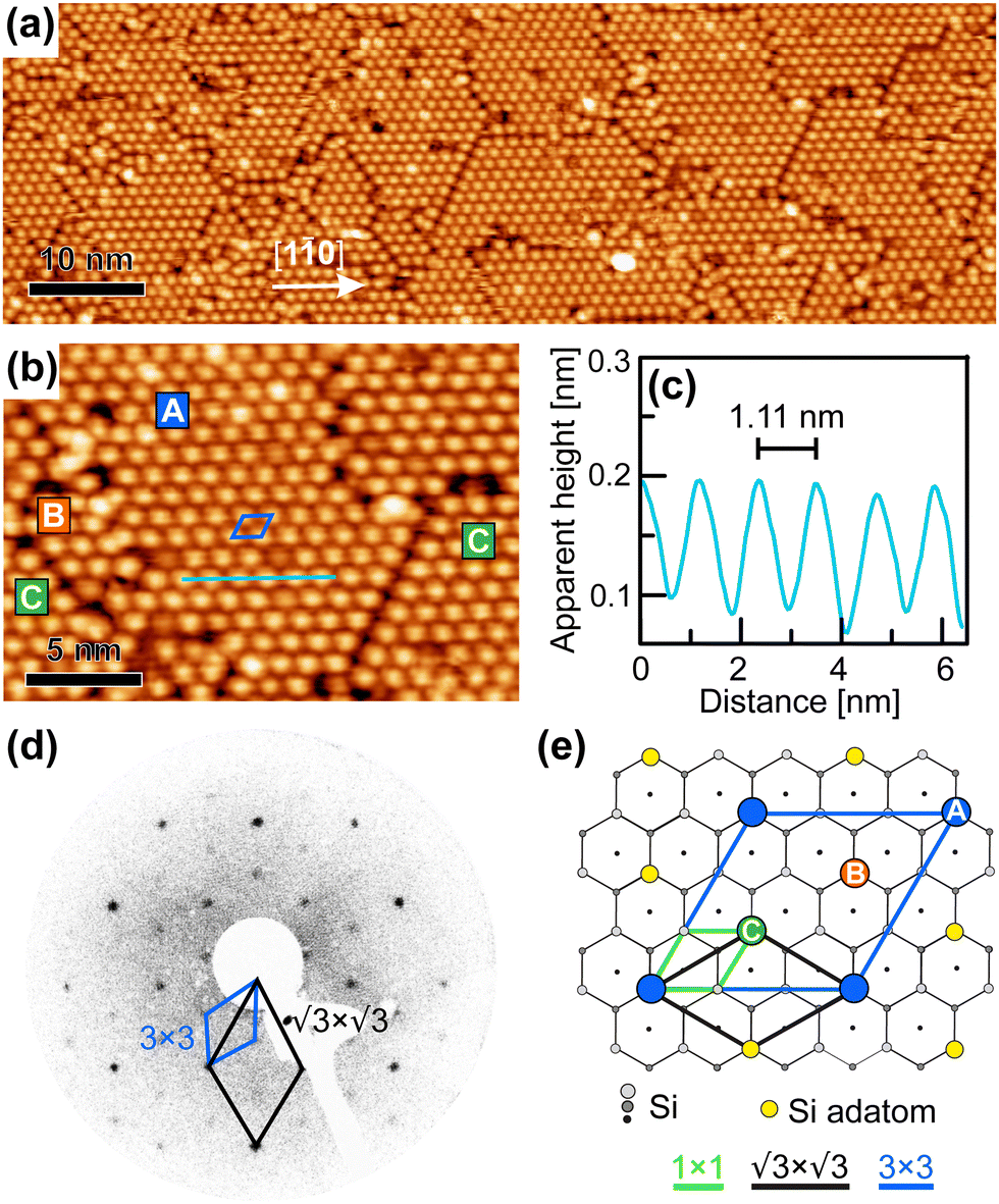 | ||
| Fig. 4 (a) Overview STM image with a full monolayer coverage (VS = −2.5 V, IT = 15 pA) and (b) more detailed image with a marked unit cell. (c) Height profile inside a domain along the line in (b) showing a 3 × 3 periodicity that is supported by LEED at a kinetic energy of 50 eV shown in (d). (e) Structure model of the ordered cyCAAC monolayer with the 3 × 3 unit cell marked in blue and the three different sublattice adsorption positions A, B and C indicated exemplarily by blue, green, and orange circles, respectively. | ||
In Fig. 4(e), the top view of the Si(111)–B structure model is shown with the adsorption sites and the unit cell of the 3 × 3 cyCAAC layer indicated. Due to the three times larger size of the 3 × 3 unit cell of the cyCAAC monolayer as compared to the one of the  R30° substrate reconstruction, three adatoms are present in one unit cell corresponding to three equivalent sublattices (labelled A, B, and C). An adsorption of the cyCAAC molecules on different sublattices then leads to different registries with respect to the substrate
  R30° lattice, so that domains formed on different sublattices cannot merge when meeting each other. In such cases, these different domains, which are labelled as A, B, and C in Fig. 4(b) according to their sublattice registry, are separated by domain boundaries.
In our STM measurements of the full cyCAAC coverage, we only find step heights corresponding to multiples of Si(111) atomic steps (see Section 6 of the ESI†). Furthermore, no additional cyCAAC islands are found in the STM images. These findings strongly suggest that the stable coverage in UHV saturates at one monolayer for room-temperature deposition and no further cyCAAC layers are formed on the top.
Si(111)–B wafers with much lower B doping were used for comparison concerning the defect density on the clean surface and the magnitude of ordering after the full coverage with cyCAAC molecules, as shown in Fig. 5(a and b), respectively. It is already obvious from the visual inspection of Fig. 5(a) that the substrate is characterized by a rather high defect density. By counting the visible defects in large-scale STM images, as described in Section 4 of the ESI,† a defect density of 1.2% of Si adatoms is found for the higher doped wafers, while the lower doped ones have a defect density of around 9.6%. Thus, the surface defect density of the lower doped wafers is by a factor of ∼8 higher. While the Si–Si(S5) point defect is the dominant defect on the surface of the higher doped wafer, the same behavior can be expected for the lower doped ones, an assumption that is further supported by the similar appearance shown in the inset of Fig. 5(a). Thus, the dominant features in Fig. 5(a), being those with the medium contrast, are assigned to the Si–Si(S5) defects.
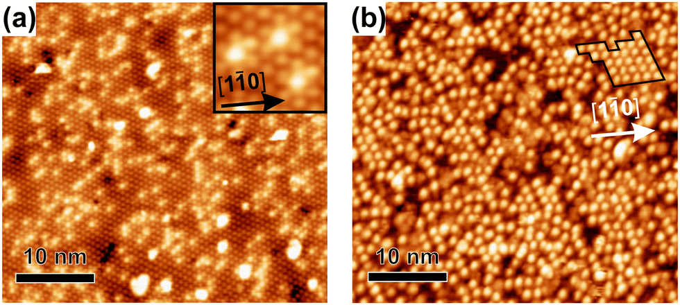 | ||
| Fig. 5 (a) Clean surface of the lower doped wafer (VS = +1.8 V, IT = 50 pA). (b) Typical STM overview image after the full cyCAAC coverage on the lower doped wafer (VS = −2.5 V, IT = 15 pA). | ||
It is found that the defect density correlates with the observed domain sizes of the cyCAAC monolayers: The average domain size when using a higher doped wafer is about 130 nm2, while for the lower doped wafer only a few molecules form an ordered structure that can be summarized as a domain, see Fig. 5(b) and ESI† Section 5. An exceptionally large domain is marked in Fig. 5(b). On this wafer, the typical domain size amounts to 10–20 nm2, being about a factor of 10 smaller than that for the higher doped sample, a value that correlates nicely with the ∼8 times higher defect density. This behavior strongly indicates that the formation of the domains is related to the defects, where the domain formation process begins with a single molecule binding to a specific site. Here, the Si–Si(S5) defect seems to be this preferred binding site as also observed in other cases,17 forming a rather strong covalent bond with a molecule and thereby preventing its further lateral movement, thus serving as a nucleation center. Molecules impacting on the regular surface structure seem to bind less strongly resulting in sufficient mobility to change their position until they are adsorbed on the correct sublattice. Chains and moreover wide domains can thereby be formed and grow in size until the growth is limited by another domain that started at a different 3 × 3 sublattice. It is interesting to note that the domain sizes correlate quantitatively with the defect densities: At the higher doped sample with a 1.2% defect density, one defect corresponds to a surface area of ∼33 nm2. This value is smaller than the average domain size of ∼130 nm2, which is a reasonable deviation when considering that domains originating from defects on the same 3 × 3 sublattice will merge when touching each other.
It should be noted that the mechanism described above cannot alone explain the large domains found for the ordered cyCAAC monolayer. When analysing the adsorption sites of molecules in the low coverage STM images (Fig. 3) with respect to their sublattices, the distances between molecules adsorbed on different sublattices are much smaller than the typical domain sizes observed for the 3 × 3 monolayer. Thus, as already discussed in our previous work,19 a ripening mechanism has to act during growth, in which already adsorbed molecules hop to an adjacent site. The energy necessary for this kinetic process may be provided thermally or by collisions with impinging molecules from the gas phase or with other diffusing molecules.
A particularly interesting property previously reported for NHC monolayers on surfaces is their large work function reduction.19,48 In order to investigate, if also the formation of the cyCAAC monolayer is accompanied by such an effect, the work function difference ΔW between the clean Si(111)–B surface and the one covered by the full monolayer of cyCAAC was determined by measuring the secondary electron onsets using XPS (see Section 2.3 of the ESI† for more details regarding the measurement).
The results for both investigated Si(111)–B wafers are shown in Fig. 6. In both cases, a shift to lower kinetic energies shows a reduction of the work function. The values of the reduction determined from linear fits to the onsets (shown as dashed gray lines), however, differ considerably for the two wafers. While for the higher doped wafer (i.e. the wafer with the lower surface defect density) a large reduction by ΔW = −1.86 eV is found, the value is considerably smaller for the lower doped wafer with the higher surface defect density, showing only a reduction by ΔW = −1.24 eV. To ensure that no other adsorbates that could influence the work function like e.g. oxygen are present on the samples investigated here, XPS overview spectra are presented in the ESI† Section 7 demonstrating the cleanliness of our preparation. The reduction found for the highly ordered cyCAAC monolayer on the wafer with low defect density is comparable to the values found for other NHCs on Si(111)–B and Au.19,48 It is assigned to two processes: first, the charge transfer between the molecules and the substrate due to the strong donor capabilities of CAACs and second, to the orientation of the molecular dipole on the surface. The 0.62 eV smaller work function reduction for the lower doped substrate can be assigned to two effects: first, the 0.39 eV lower work function of the clean surface as revealed by the shifted onset with respect to the one for the higher doped substrate (green curves in Fig. 6), related to a different band bending due to the higher surface defect density, and second, a 0.23 eV higher final work function for the monolayer on the lower doped substrate (red curves in Fig. 6) that has a smaller area density of molecules because of the domain boundaries.
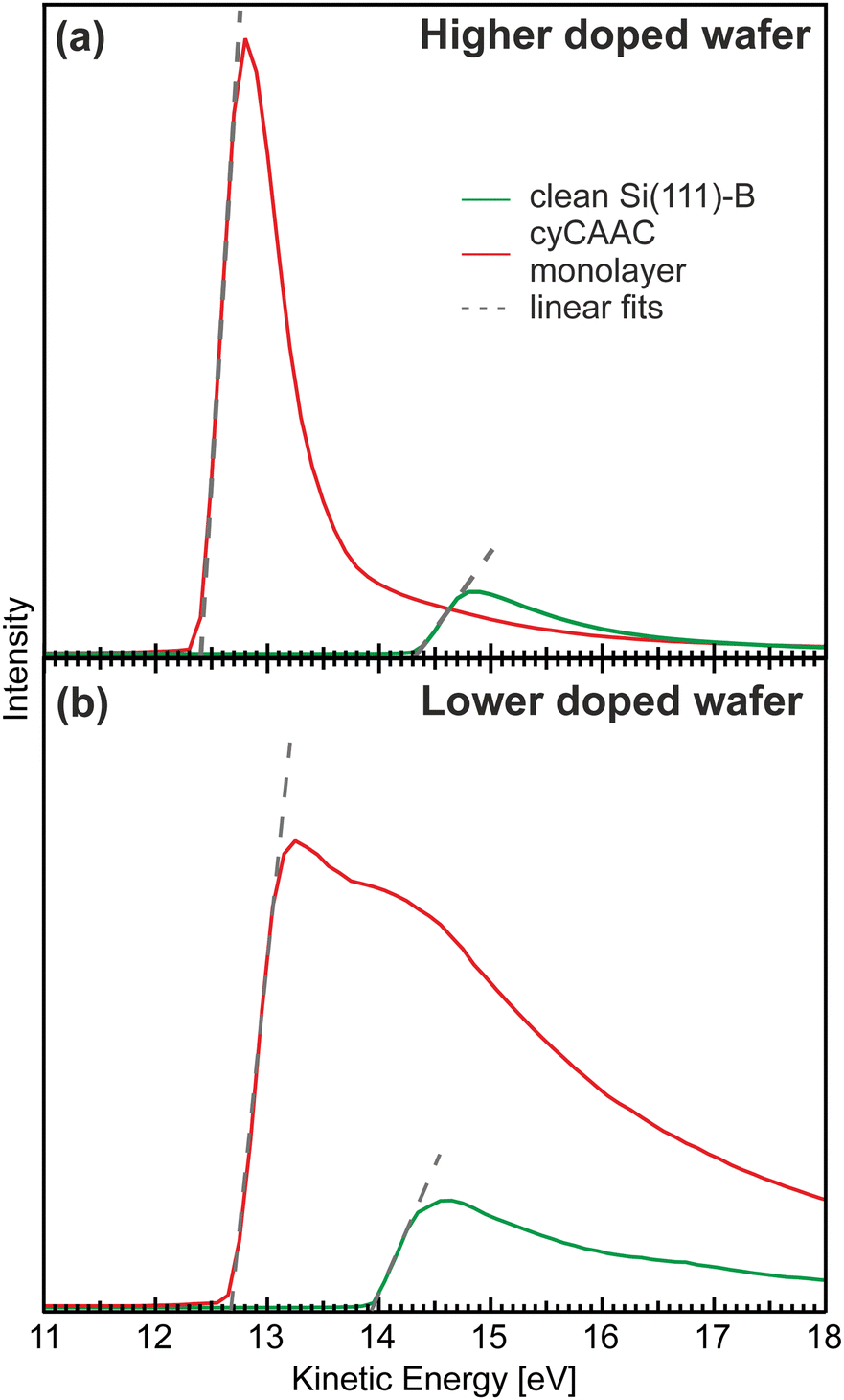 | ||
| Fig. 6 Secondary electron onsets measured using XPS for the clean Si(111)–B samples (green) and cyCAAC monolayers (red) on (a) the higher doped wafer and (b) the lower doped wafer. The gray dashed lines show the linear fits to the onsets used to determine the work function changes. Note that the kinetic energy is shifted due the application of a bias of −9 V to the sample. | ||
Conclusions
In this work, it was shown that cyCAAC forms a well ordered, stable monolayer on the Si(111) R30°–B surface by a particular self-limited growth. The molecules adsorb in an upright geometry, forming a covalent bond with the substrate Si adatoms. Single molecules seem to rotate and/or vibrate due to their thermal energy, similar to that observed for other NHC molecules on this surface.19
A highly ordered monolayer with a 3 × 3 periodicity and large domain sizes is formed for a full cyCAAC coverage on a surface with a lower density of Si–Si(S5) defects. On a substrate with a higher density of such defects, in contrast, no extensive ordering can be achieved. This surface defect density, which can be adjusted by the level of B doping, is thus found to have a significant impact on the magnitude of ordering in the monolayer. A lower surface defect density results in wide ordered domains, while a higher defect density leads to smaller domain sizes, revealing that the defect site on which the initial adsorption of the molecules occurs is the nucleation center for the domain growth. In the present material system, the surface defect density thus does not only determine the defect density of the overlayer, but also directly influence the domain sizes.
The cyCAAC monolayer furthermore leads to strong changes in the electronic properties of the surface, as demonstrated by the observation of a large reduction of the work function upon cyCAAC adsorption on the substrate with a low surface defect density. The differences in the work functions of the two wafers covered with cyCAAC monolayers underpin the importance of a highly ordered monolayer for an efficient surface functionalization.
Conflicts of interest
There are no conflicts to declare.Acknowledgements
Generous financial support by the Ministry for Culture and Science NRW, the Governing Mayor of Berlin-Senate Chancellery Higher Education and Research, the German Federal Ministry of Education and Research (BMBF) and the Deutsche Forschungsgemeinschaft (SFB 858, Leibniz Award) is gratefully acknowledged. R. Z. acknowledges financial support by the Elsa-Neumann-Stipendium des Landes Berlin (NaFöG).References
- H. Neergaard Waltenburg and J. Yates, Chem. Rev., 1995, 95, 1589 CrossRef.
- R. J. Hamers, Annu. Rev. Anal. Chem., 2008, 1, 707 CrossRef CAS PubMed.
- J. Ren, M. Freitag, Y. Gao, P. Bellotti, M. Das, B. Schulze Lammers, H. Mönig, Y. Zhang, C. G. Daniliuc, S. Du, H. Fuchs and F. Glorius, Angew. Chem., Int. Ed., 2022, 61, e202115104 CAS.
- J. J. Navarro, M. Das, S. Tosoni, F. Landwehr, M. Koy, M. Heyde, G. Pacchioni, F. Glorius and B. Roldan Cuenya, Angew. Chem., Int. Ed., 2022, 61, e202202127 CAS.
- J. C. Love, L. A. Estroff, J. K. Kriebel, R. G. Nuzzo and G. M. Whitesides, Chem. Rev., 2005, 105, 1103 CrossRef CAS PubMed.
- C. D. Bain, E. B. Troughton, Y. T. Tao, J. Evall, G. M. Whitesides and R. G. Nuzzo, J. Am. Chem. Soc., 1989, 111, 321 CrossRef CAS.
- C. M. Crudden, J. H. Horton, I. I. Ebralidze, O. V. Zenkina, A. B. McLean, B. Drevniok, Z. She, H.-B. Kraatz, N. J. Mosey, T. Seki, E. C. Keske, J. D. Leake, A. Rousina-Webb and G. Wu, Nat. Chem., 2014, 6, 409 CrossRef CAS PubMed.
- G. Wang, A. Rühling, S. Amirjalayer, M. Knor, J. B. Ernst, C. Richter, H.-J. Gao, A. Timmer, H.-Y. Gao, N. L. Doltsinis, F. Glorius and H. Fuchs, Nat. Chem., 2017, 9, 152 CrossRef CAS PubMed.
- C. R. Larrea, C. J. Baddeley, M. R. Narouz, N. J. Mosey, J. H. Horton and C. M. Crudden, ChemPhysChem, 2017, 18, 3536 CrossRef CAS PubMed.
- A. Bakker, A. Timmer, E. Kolodzeiski, M. Freitag, H. Y. Gao, H. Mönig, S. Amirjalayer, F. Glorius and H. Fuchs, J. Am. Chem. Soc., 2018, 140, 11889–11892 CrossRef CAS PubMed.
- G. Lovat, E. A. Doud, D. Lu, G. Kladnik, M. S. Inkpen, M. L. Steigerwald, D. Cvetko, M. S. Hybertsen, A. Morgante, X. Roy and L. Venkataraman, Chem. Sci., 2019, 10, 930 RSC.
- M. Koy, P. Bellotti, M. Das and F. Glorius, Nat. Catal., 2021, 4, 352–363 CrossRef CAS.
- S. R. Wagner, R. R. Lunt and P. Zhang, Phys. Rev. Lett., 2013, 110, 086107 CrossRef PubMed.
- S. R. Wagner, B. Huang, C. Park, J. Feng, M. Yoon and P. Zhang, Phys. Rev. Lett., 2015, 115, 096101 CrossRef PubMed.
- Y. Makoudi, J. Jeannoutot, F. Palmino, F. Chérioux, G. Copie, C. Krzeminski, F. Cleri and B. Grandidier, Surf. Sci. Rep., 2017, 72, 316 CrossRef CAS.
- S. Lindner, M. Franz, M. Kubicki, S. Appelfeller, M. Dähne and H. Eisele, Phys. Rev. B, 2019, 100, 245301 CrossRef CAS.
- M. Kubicki, S. Lindner, M. Franz, H. Eisele and M. Dähne, J. Vac. Sci. Technol., B, 2020, 38, 042803 CrossRef CAS.
- H. Aldahhak, C. Hogan, S. Lindner, S. Appelfeller, H. Eisele, W. Schmidt, M. Dähne, U. Gerstmann and M. Franz, Phys. Rev. B, 2021, 103, 035303 CrossRef CAS.
- M. Franz, S. Chandola, M. Koy, R. Zielinski, H. Aldahhak, M. Das, M. Freitag, U. Gerstmann, D. Liebig, A. K. Hoffmann, M. Rosin, W. G. Schmidt, C. Hogan, F. Glorius, N. Esser and M. Dähne, Nat. Chem., 2021, 13, 828 CrossRef CAS PubMed.
- R. L. Headrick, I. K. Robinson, E. Vlieg and L. C. Feldman, Phys. Rev. Lett., 1989, 63, 1253–1256 CrossRef CAS PubMed.
- P. Bedrossian, R. D. Meade, K. Mortensen, D. M. Chen, J. A. Golovchenko and D. Vanderbilt, Phys. Rev. Lett., 1989, 63, 1257–1260 CrossRef CAS PubMed.
- R. Jazzar, R. D. Dewhurst, J.-B. Bourg, B. Donnadieu, Y. Canac and G. Bertrand, Angew. Chem., Int. Ed., 2007, 46, 2899–2902 CrossRef CAS PubMed.
- D. A. Ruiz, G. Ung, M. Melaimi and G. Bertrand, Angew. Chem., Int. Ed., 2013, 52, 7590 CrossRef CAS PubMed.
- M. N. Hopkinson, C. Richter, M. Schedler and F. Glorius, Nature, 2014, 510, 485 CrossRef CAS PubMed.
- M. Soleilhavoup and G. Bertrand, Acc. Chem. Res., 2015, 48, 256 CrossRef CAS.
- M. Melaimi, R. Jazzar, M. Soleilhavoup and G. Bertrand, Angew. Chem., Int. Ed., 2017, 56, 10046 CrossRef CAS PubMed.
- S. Amirjalayer, A. Bakker, M. Freitag, F. Glorius and H. Fuchs, Angew. Chem., Int. Ed., 2020, 59, 21230 CrossRef CAS PubMed.
- R. Jazzar, M. Soleilhavoup and G. Bertrand, Chem. Rev., 2020, 120, 4141 CrossRef CAS PubMed.
- P. Bellotti, M. Koy, M. N. Hopkinson and F. Glorius, Nat. Rev. Chem., 2021, 5, 711–725 CrossRef CAS PubMed.
- L. Marzo, Eur. J. Org. Chem., 2021, 4603–4610 CrossRef CAS.
- A. V. Zhukhovitskiy, M. G. Mavros, T. Van Voorhis and J. A. Johnson, J. Am. Chem. Soc., 2013, 135, 7418 CrossRef CAS PubMed.
- A. V. Zhukhovitskiy, M. J. MacLeod and J. A. Johnson, Chem. Rev., 2015, 115, 11503 CrossRef CAS PubMed.
- A. V. Zhukhovitskiy, M. G. Mavros, K. T. Queeney, T. Wu, T. Van Voorhis and J. A. Johnson, J. Am. Chem. Soc., 2016, 138, 8639 CrossRef CAS.
- J. B. Ernst, S. Muratsugu, F. Wang, M. Tada and F. Glorius, J. Am. Chem. Soc., 2016, 138, 10718–10721 CrossRef CAS PubMed.
- C. M. Crudden, J. H. Horton, M. R. Narouz, Z. Li, C. A. Smith, K. Munro, C. J. Baddeley, C. R. Larrea, B. Drevniok, B. Thanabalasingam, A. B. McLean, O. V. Zenkina, I. I. Ebralidze, Z. She, H.-B. Kraatz, N. J. Mosey, L. N. Saunders and A. Yagi, Nat. Commun., 2016, 7, 12654 CrossRef CAS PubMed.
- J. B. Ernst, C. Schwermann, G.-I. Yokota, M. Tada, S. Muratsugu, N. L. Doltsinis and F. Glorius, J. Am. Chem. Soc., 2017, 139, 9144 CrossRef CAS PubMed.
- C.-Y. Wu, W. J. Wolf, Y. Levartovsky, H. A. Bechtel, M. C. Martin, F. D. Toste and E. Gross, Nature, 2017, 541, 511–515 CrossRef CAS PubMed.
- R. Ye, A. V. Zhukhovitskiy, R. V. Kazantsev, S. C. Fakra, B. B. Wickemeyer, F. D. Toste and G. A. Somorjai, J. Am. Chem. Soc., 2018, 140, 4144–4149 CrossRef CAS PubMed.
- A. Lv, M. Freitag, K. M. Chepiga, A. H. Schäfer, F. Glorius and L. Chi, Angew. Chem., Int. Ed., 2018, 57, 4792 CrossRef CAS PubMed.
- D. T. Nguyen, M. Freitag, M. Körsgen, S. Lamping, A. Rühling, A. H. Schäfer, M. H. Siekman, H. F. Arlinghaus, W. G. van der Wiel, F. Glorius and B. J. Ravoo, Angew. Chem., Int. Ed., 2018, 57, 11465 CrossRef CAS PubMed.
- N. Kaeffer, H.-J. Liu, H.-K. Lo, A. Fedorov and C. Copéret, Chem. Sci., 2018, 9, 5366 RSC.
- C. Smith, M. R. Narouz, P. A. Lummis, I. Singh, A. Nazemi, C.-H. Li and C. M. Crudden, Chem. Rev., 2019, 119, 4986 CrossRef CAS PubMed.
- D. T. Nguyen, M. Freitag, C. Gutheil, K. Sotthewes, B. J. Tyler, M. Böckmann, M. Das, F. Schlüter, N. L. Doltsinis, H. F. Arlinghaus, B. J. Ravoo and F. Glorius, Angew. Chem., Int. Ed., 2020, 59, 13651 CrossRef CAS PubMed.
- R. J. Lewis, M. Koy, M. Macino, M. Das, J. H. Carter, D. J. Morgan, T. E. Davies, J. B. Ernst, S. J. Freakley, F. Glorius and G. J. Hutchings, J. Am. Chem. Soc., 2022, 144, 15431 CrossRef CAS PubMed.
- V. Lavallo, Y. Canac, C. Präsang, B. Donnadieu and G. Bertrand, Angew. Chem., Int. Ed., 2005, 44, 5705 CrossRef CAS PubMed.
- A. Bakker, M. Freitag, E. Kolodzeiski, P. Bellotti, A. Timmer, J. Ren, B. Schulze Lammers, D. Moock, H. W. Roesky, H. Mönig, S. Amirjalayer, H. Fuchs and F. Glorius, Angew. Chem., Int. Ed., 2020, 59, 13643 CrossRef CAS PubMed.
- L. Meier and W. G. Schmidt, J. Phys. Chem. C, 2023, 127, 1973–1980 CrossRef CAS.
- H. K. Kim, A. S. Hyla, P. Winget, H. Li, C. M. Wyss, A. J. Jordan, F. A. Larrain, J. P. Sadighi, C. Fuentes-Hernandez, B. Kippelen, J.-L. Bredas, S. Barlow and S. R. Marder, Chem. Mater., 2017, 29, 3403–3411 CrossRef CAS.
Footnote |
| † Electronic supplementary information (ESI) available: Synthesis of the CAAC precursors, details of sample preparation and experimental methods, NMR spectra, additional experimental data, and detailed description of substrate properties and analysis. See DOI: https://doi.org/10.1039/d3tc00681f |
| This journal is © The Royal Society of Chemistry 2023 |