
 Open Access Article
 This Open Access Article is licensed under a Creative Commons Attribution-Non Commercial 3.0 Unported Licence
From synthesis to device fabrication: elucidating the structural and electronic properties of C7-BTBT-C7†
Priya
Pandey
 ab,
Lamiaa
Fijahi
c,
Nemo
McIntosh
d,
Nicholas
Turetta
e,
Marco
Bardini
d,
Samuele
Giannini
d,
Christian
Ruzié
f,
Guillaume
Schweicher
f,
David
Beljonne
d,
Jérôme
Cornil
d,
Paolo
Samorì
e,
Marta
Mas-Torrent
*c,
Yves Henri
Geerts
*fg,
Enrico
Modena
*a and
Lucia
Maini
*b
ab,
Lamiaa
Fijahi
c,
Nemo
McIntosh
d,
Nicholas
Turetta
e,
Marco
Bardini
d,
Samuele
Giannini
d,
Christian
Ruzié
f,
Guillaume
Schweicher
f,
David
Beljonne
d,
Jérôme
Cornil
d,
Paolo
Samorì
e,
Marta
Mas-Torrent
*c,
Yves Henri
Geerts
*fg,
Enrico
Modena
*a and
Lucia
Maini
*b
aPolyCrystalLine SPA, Via Della Cooperazione, 29 40059 Medicina, Bologna, Italy
bDipartimento di Chimica “G. Ciamician”, via Selmi 2 – Università di Bologna, I-40126, Bologna, Italy
cInstitut de Ciència de Materials de Barcelona (ICMAB-CSIC), Campus de la UAB, 08193, Bellaterra, Spain
dLaboratory for Chemistry of Novel Materials, University of Mons, 7000 Mons, Belgium
eUniversity of Strasbourg, CNRS, ISIS UMR 7006, 8 Alleé Gaspard Monge, Strasbourg, F-67000, France
fLaboratoire de Chimie des Polymères, Faculté des Sciences, Université Libre de Bruxelles (ULB), CP 206/1 Boulevard du Triomphe, 1050 Bruxelles, Belgium
gInternational Solvay Institutes, Université Libre de Bruxelles (ULB), CP 231 Boulevard du Triomphe, 1050, Bruxelles, Belgium
First published on 21st April 2023
Abstract
We report the polymorph investigation, crystallographic study and fabrication of organic field-effect transistors (OFETs) in solution-processed thin films of a prototypical organic semiconductor, i.e., 2,7-diheptylbenzo[b]benzo[4,5]thieno[2,3-d]thiophene (C7-BTBT-C7). We found that this molecule self-assembles solely into one type of stable crystal form, regardless of the experimental conditions employed when using conventional and non-conventional methods of crystallization. The integration of blends of C7-BTBT-C7 with polystyrene as active materials in OFETs fabricated using a solution shearing technique led to a field-effect mobility of 1.42 ± 0.45 cm2 V−1 s−1 in the saturation regime when a coating speed of 10 mm s−1 was employed. The intrinsic structural properties control the overlap of the frontier orbitals, thereby affecting the device performance. The interplay between the crystal packing, thin film morphology and uniformity and its impact on the device performance are reported.
Introduction
The use of organic compounds as active layers in organic field-effect transistors (OFETs) has been thoroughly explored during the past few decades.1–3 One of the major advantages of organic semiconductors (OSCs) is that their physical and chemical properties can be finely tuned via ad hoc chemical design.4–8 Charge carrier mobility, which is the ability to transport electrical charges (defined as the derivative of the drift velocity of the charge carrier (cm s−1) with respect to the applied electric field (V cm−1)), is a property intrinsic to a material, and it depends on its structure at the molecular and supramolecular levels.9 The structure of solution-processable OSCs typically consists of (i) π-conjugated cores or backbones, which mainly determine the optoelectronic properties of the material, and (ii) non-conjugated side groups, which govern the solubility, crystalline packing, morphology, and microstructure of the thin film. A steady development of molecular design strategies has been made toward improving charge transport properties.2,9–11When dealing with small organic molecules, it is crucial to investigate polymorphism, as organic molecules are prone to self-assemble in different polymorphic forms owing to weak van der Waals interactions that prevail in the solid state.12–14 Polymorphism is not only interesting in understanding the intermolecular interactions and supramolecular chemistry but can also have a profound impact on the electronic properties on account of the structure–property relationships.15 A comprehensive study of the solid-state interactions and crystal packing can be useful to access different polymorphs depending on the competition between thermodynamics and kinetics.16,17 For example, distinct crystallization conditions can induce multiple rearrangements of the molecules resulting in different crystal packings.18,19 Finally, the electrical properties of OFETs based on OSC polymorphs vary as a response to structural changes.20 Moreover, when the molecules crystallize at a solid interface, the organization of the molecules can adapt unique interfacial packings, known as surface-induced phases (SIPs).21,22 These polymorphs might exhibit intrinsically different charge transport properties, as in the case of pentacene.23 The rigid substrate support, which acts as the nucleating agent, can, in fact, propel a different reorganization of the molecules that locally affect the intermolecular orbital overlap.24 In bottom contact/bottom gate OFETs, the charge transport processes occur within the first few molecular layers adjacent to the dielectric surface.25 Therefore, gaining insight into the exact molecular packing in thin films is of utmost importance for a complete understanding of and control over the structure–property relationships.
Another aspect to look at while handling OSCs is the correlation between film morphology and device performance, as the successful application of these materials in devices depends on the strategic optimization of solution-processed methods.26 The obtaining of large crystals is definitively advantageous for charge transport.27 Tailoring crystal growth conditions using deposition techniques, such as directional crystallization, offers advantages like decoupling the nucleation process from crystal growth and potential access to the uniaxial alignment of the crystallites.28 Providing non-equilibrium dissipative conditions on the crystal growth of organic compounds, with the aid of such a method, we can control the number of molecules entering the crystal phase per unit of time in specific crystallographic directions. Directional crystallization helps us in understanding the impact of each condition on the crystalline morphology, crystal structure, crystal growth rate, thermal gradient magnitude, and polymorph formation of a preferably oriented thin film.29 In addition to the thermal gradient technique for directional crystallization, we also explored a solution coating technique, another non-equilibrium dissipative method. Solution shearing, compatible with roll-to-roll fabrication processes, has been evolving recently due to its benefits like large-area coverage and low-cost manufacture.16 In particular, in the bar-assisted meniscus shearing (BAMS) technique,30,31 it has been shown that the substrate temperature, deposition speed, and OSC ink formulation play a crucial role in the thermodynamics and kinetics of the crystallization process. Hence, these parameters have been exploited to control the thin film polymorphism.32–35
Aiming to explore and control polymorphism, the ideal candidate for fabricating thin films by solution shearing must possess good solubility in most organic solvents. Numerous scientific groups have been studying [1]benzothieno[3,2-b][1]benzothiophene (BTBT) π-conjugated molecules as archetypical systems.36–38 The high solution-processability and chemical stability of the functionalized BTBT lead these small-molecule OSCs a step closer to their use in electronic applications, where low cost, large-area coverage, and structural flexibility are required.39 Among the BTBT derivatives, C8-BTBT-C8 has demonstrated remarkably high field-effect mobility values.31,40,41 Therefore, we designed and synthesized a BTBT derivative bearing similar alkyl side chains with an odd number of carbons to evaluate the odd–even effect on the molecular packing, polymorphism, and electronic properties.42 We thus studied a p-type semiconductor 2,7-diheptylbenzo[b]benzo[4,5]thieno[2,3-d]thiophene (C7-BTBT-C7), typically comprising a rigid aromatic core (BTBT) and flexible peripheral chains (C7) (Scheme 1).43 Likewise, C8-BTBT-C8 and C7-BTBT-C7 also exhibit a mesophase, which, in our case, is a thermotropic liquid crystal. The liquid crystal phase might be advantageous for processing molecular semiconductors and controlling the structural order in the bulk and at interfaces.44
 | ||
| Scheme 1 Chemical structure of C7-BTBT-C7. | ||
Herein, we report the extensive polymorph screening of C7-BTBT-C7 in the bulk, with particular attention to establishing if the same crystal phase is also present in thin films fabricated using multiple deposition techniques. We also looked into the possible odd–even effect of the side chains by performing a comparative study using C8-BTBT-C8 as a reference. We found that the molecular packing strongly affects the ionization potential, the transfer integrals, and the charge transport behaviour. The combination of all these findings was key to understand in depth the electrical properties of C7-BTBT-C7-based OFETs.
Results and discussion
Polymorph screening
C7-BTBT-C7 was found to be soluble in a multitude of organic solvents (see Table S1, ESI†). C7-BTBT-C7 is prone to form crystals; hence, it could be recrystallized in various solvents by evaporation. Besides evaporation, we also explored methods like anti-precipitation, slurry, mechanochemistry, and controlled recrystallization by Crystal16 (the Crystal16 parallel crystallizer is an instrument that allows testing of a wide diversity of crystallization conditions such as solvents and solvent mixtures, compound concentrations, counter-ions, and temperature profiles.). However, no other polymorphs were observed, and all the experiments resulted in the same crystalline phase as the starting material (Fig. 1 and Fig. S2a, ESI†). | ||
| Fig. 1 XRD comparison of the experimental pattern collected from transmission geometry (red) and the simulated pattern from SCXRD (black) at 25 °C, indicating the same phase of the crystal (λ = 0.9999613 Å). The ordinate scale is in square root. | ||
Structural characterization by single-crystal X-ray diffraction
Crystals obtained by slow evaporation of C7-BTBT-C7 in a PXY solvent were selected for SCXRD analysis. Even though the crystals were very thin plates stacked over one another, the SCXRD collection led to good-quality data. The structure was resolved in a monoclinic space group P21/c with a half molecule in the asymmetric unit (Table S2, ESI†). The molecule carries a rigid flat core and flexible alkyl chains. As commonly observed for BTBT molecules, C7-BTBT-C7 exhibits herringbone packing, with a herringbone angle of 56.5(1)° and a core-tilt angle of 87.7(1)°, indicating that the core remains almost upright (Fig. 2(a) and (b)). In addition, the length of the molecule was found to correspond to the interlayer distance, as presented in Fig. 3. This interlayer distance remains intact even upon conversion of the crystal to the liquid crystal phase (see later).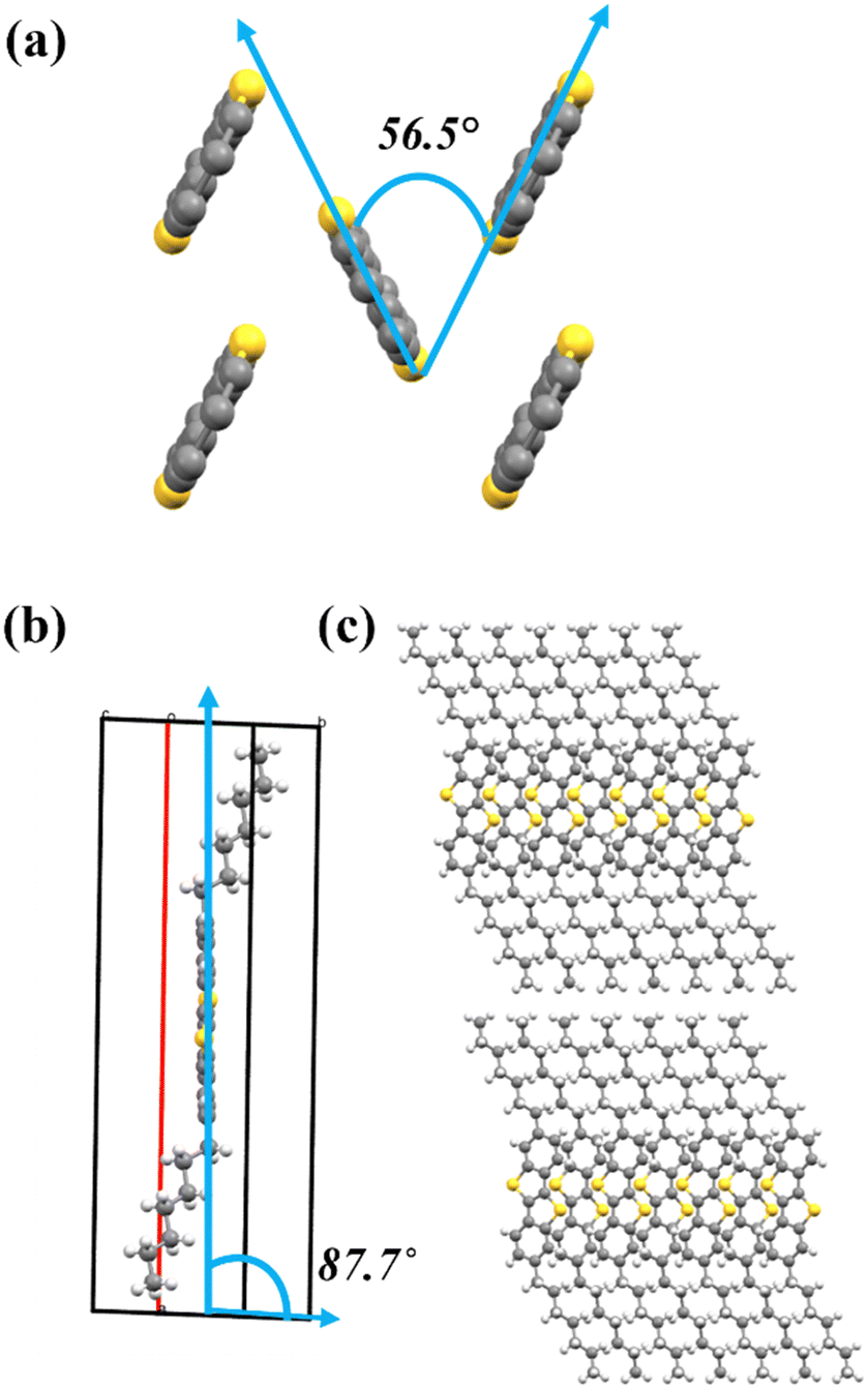 | ||
| Fig. 2 Crystal structures: (a) herringbone angle, (b) core-tilt angle, and (c) layered packing along the b-axis. | ||
 | ||
| Fig. 3 Schematic representation of the C7-BTBT-C7 molecular structure and surface arrangement on SiO2 indicating an interlayer spacing (d) of 26 Å calculated from XRD measurements. | ||
Compared to similar BTBT derivatives with even chain lengths like C8-BTBT-C845 and C12-BTBT-C12,3 we discovered that C7-BTBT-C7 is isomorphous with both (Table S3, ESI†). However, despite the similar parameters, it is worth noting that there are no short contacts between the cores of C7-BTBT-C7, whereas there are short contact interactions in C8-BTBT-C8 and C12-BTBT-C12 (Fig. S3, ESI†). This agrees with the decreasing trend of the herringbone angle observed from C7 (56.5(1)°) to C8 (54.9(1)°) to C12 (53.9(1)°); the molecular packing seems to tighten from C7 → C8 → C12 BTBTs and thus attributing to the increasing short contacts from C7 → C8 → C12 BTBTs. We examined all the other packing parameter descriptors of these molecules and did not witness any significant difference in the structure apart from longer alkyl chains. Also, the different orientation of the final carbon due to the odd–even alkyl chains does not influence the core-tilt angle, which remains constant.
The intermolecular interactions in the crystal structure were further analysed by Hirshfeld surface analysis using the CrystalExplorer17 software package. The 3D visualization of electron density and the dnorm plots provides an idea of the interaction's contributions in molecular packing. Unlike C8-BTBT-C8 and C12-BTBT-C12, there were only white and blue regions, which indicate that the interactions are equal to and greater than the van der Waals distance, respectively, while there were no red regions with the intermolecular distance being shorter than the van der Waals distance (Fig. S4a, ESI†). This confirms our statement above that stronger interactions are observed in BTBTs decorated with longer chains because of shorter roll angles.
From the fingerprint plots, it was clear that the contribution of the intermolecular interactions is dominated mainly by H–H (72.3%) and C–H (15.7%) and the rest by other interactions like S–C (6.9%), H–S (2.8%) and S–S (2.3%) (Fig. S4b, ESI†).
Thermal properties and phase transitions
Thermo-gravimetric analysis-evolved gas analysis (TGA) investigations revealed that C7-BTBT-C7 is stable up to 406 °C (Fig. S5a, ESI†) and the differential scanning calorimetry (DSC) analyses made it possible to investigate the thermal stability and temperature-dependent phases. DSC results indicated that such a molecule undergoes a reversible solid–liquid crystal transition at 107 °C followed by melting at 128 °C, whereas, by cooling, the liquid crystal recrystallizes at 98 °C (Fig. S5b, ESI†). This result is in complete agreement with previous results obtained on C8-BTBT-C8 presenting a similar SmA phase at 110 °C.45 The temperature-dependent phase transitions were also confirmed by variable-temperature X-ray diffraction (Fig. 4). At 113 °C, a phase transition from the solid to the liquid crystal was observed, and only the first peak was observed, which is consistent with the previous discussion.36 Thermal behaviours discussed above have also been qualitatively supported by hot-stage microscopy analysis on crystals (Fig. 4 and Fig. S6, ESI†).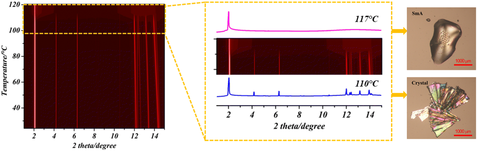 | ||
| Fig. 4 VTXRD (λ = 0.9999613 Å) showing the crystal to liquid crystal phase transition. HSM images on the right for the crystal and liquid crystal are also presented. | ||
Ionization energy
The ionization energy (IE) of the C7-BTBT-C7 powder has been determined via photoemission yield spectroscopy (PYS) in ambient air (Table S4, ESI†). The estimated IE of the compound (5.28 eV) agrees with the typical values of Cn-BTBT-Cn that have revealed IE values around 5.3 eV for 5 < n < 14.11Transfer integrals and coupling–sign relationship
Fig. 5 displays the transfer integrals superior to 10 meV computed in the C7-BTBT-C7 crystal structure. They all lie within a 2D layer, while the transfer integrals between molecules of different layers are one thousand times smaller. In light blue, we display interactions between inequivalent molecules (i.e., T1 and T2 pairs), while in red between molecules along the b direction (i.e., P pair). The values are reported in Table S5 (ESI†), along with the same transfer integrals computed for C8-BTBT-C846 and C12-BTBT-C1237 based on their crystalline structures. In Table S5 (ESI†), we also report the computed internal reorganization energy, which is around 244 meV for all the three systems investigated. Notably, analogous to the C8- and C12-derivatives, the larger transfer integral in C7-BTBT-C7 is about 50 meV, which is comparable in magnitude to the activation barrier for hole transfer between two molecules, as predicted by the semi-classical Marcus theory (i.e., λ/4).47,48 Thus, the transport in these materials is expected to be substantially different from a pure hopping model, which assumes that V ≪ λ/4 and that the charge resides on a single molecular site and moves across the material by hopping on its neighbours. As a matter of fact, the recently developed transient localization theory framework applied to C8-BTBT-C8 in ref. 49 and 50 revealed a band-like temperature dependence behaviour characteristic of the transport of delocalized charge carriers. | ||
| Fig. 5 Spatial distribution of transfer integrals in C7-, C8-, and C12-BTBT crystals in the herringbone plane. Dashed lines represent a unit cell. | ||
The transient localization theory,51,52 recently supported by explicit numerical first-principal simulations solving the coupled charge-nuclear motion,53 shows that an additional important parameter that governs charge carrier transport is the relative coupling–sign relationship of the transfer integrals associated with dimers with different transport directions.51,53 In molecular semiconductors characterized by 2D herringbone layer packing (which is common to C7-BTBT-C7 studied here as well as C8 and C12 derivatives), the charge carrier mobility is larger when the product of “signed” nearest-neighbour couplings along the three different directions is positive. Additionally, the mobility is predicted to increase when the couplings are isotropic in the plane, i.e., similar in magnitude in different crystallographic directions. The sign criterion is well satisfied by C7-BTBT-C7 (as well as by C8 and C12 derivatives), as shown in Table S5 (ESI†), where we report the signed transfer integrals computed after imposing consistent phase relationships between the wave function of the individual molecules. This supports the large experimental mobilities measured in these BTBT-derivatives, provided a good crystallinity in the device, and qualify C7-BTBT-C7 as a very good candidate to reach good performance in the term of mobility.
However, it is not straightforward to make a direct correlation between the evolution of the experimental mobility values going from C7, C8, to C12 and the changes in the transfer integrals since the calculations are performed on single crystals without any defect (like grain boundaries). The small displacements of the BTBT core in the crystal structure going from C7 to C12 are sufficient to induce significant modulations in the amplitude of the transfer integrals (from 7 meV to 47 meV) for the JT pair, as expected from the very high sensitivity of electronic couplings to the relative positions of interacting molecules. Based on the sign analysis and the isotropic character, C12-BTBT-C12 should yield the highest hole mobility in single crystals.
Directional crystallization using a temperature gradient
In our quest to explore the polymorphic landscape of the material, we investigated the use of a thermal gradient recrystallization process. We provided controlled non-equilibrium dissipative conditions on the crystal nucleation and growth of C7-BTBT-C7 using a thermal gradient. The temperature gradient technique produces films from the melt, which is rather uncommon.28 About 3–4 mg of the material was deposited on a clean glass substrate placed on the hot side of the thermal gradient setup and melted. The uniformly distributed films (thickness in μm range) are formed by sandwiching the material between two glass slides to avoid dewetting of the melt. Then, the sandwiched glass slides are translated at a constant pulling rate (μm s−1) (Fig. 6(a)). As the sample approaches the cold stage, the in situ nucleation and growth of the crystals are observed using a polarized optical microscope (POM). We varied the conditions like pulling velocities (5, 10, 25, 50, and 100 μm s−1) (Fig. S7, ESI†) and temperatures of the cold stage (Tc = 70 °C and 90 °C) to tailor the crystallization conditions. In the case of the lowest pulling velocity, the nucleation occurs in the edge, or the corner of the substrate (event 1, Fig. 6(b)), and the nucleus grows quickly towards the vertical edge in the undercooled region (event 2, Fig. 6(b)), as, primarily, the growth follows the coldest slice available and then propagates in the gradient direction.54 We observed the uniaxial alignment of crystals in the direction parallel to the thermal gradient (event 3, Fig. 6(b)) (as a function of undercooling and the growth rate) until the formation of mm2 size-aligned domains (event 4, Fig. 6(b)). For samples with higher pulling velocities, both primary and secondary nucleation sites were observed (Fig. S8a, ESI†).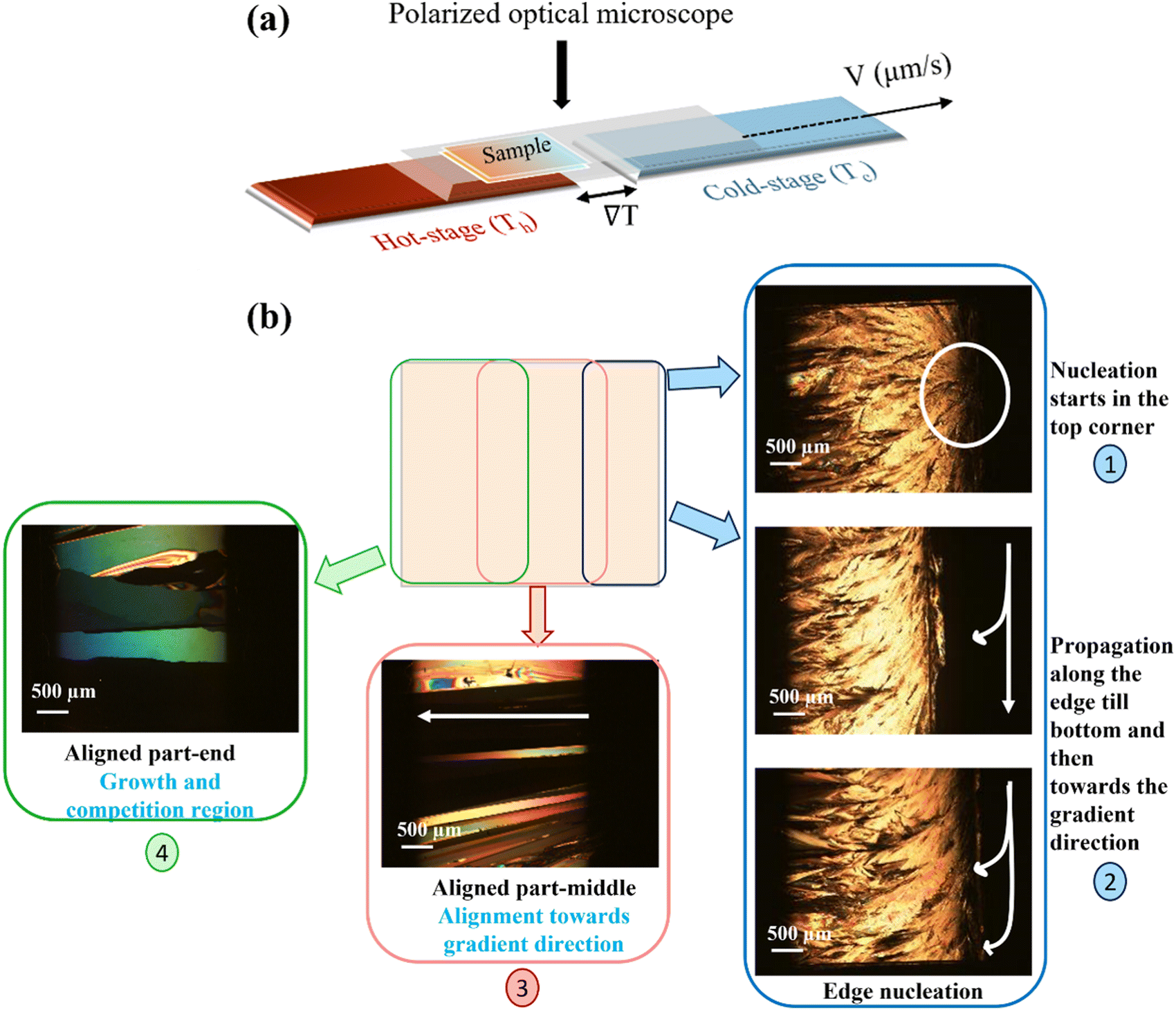 | ||
| Fig. 6 (a) Schematic representation of the thermal gradient setup and (b) polarized optical microscopy pictures recorded at room temperature after crystallization using the thermal gradient technique. Locations are indicated on the schematic representation of the sample and numbered as per the sequence of the events taking place. | ||
By observing the sample at a high temperature, we detected the liquid crystal phase, which was separated by a sharp crystal growth front as the crystallization temperature was reached, and a controlled growth was observed. Both the crystal and the liquid crystal growth fronts are straight (Fig. S8c, ESI†). By pulling the sample from the cold stage to the hot stage, we observed the transition to the liquid crystal phase, which retains the memory of the entangled ribbon-like crystals, as seen in Fig. S8b (ESI†). The degree of entanglement reduces as the pulling velocity is reduced to 5 μm s−1, where bigger domains were observed in the polycrystalline film.
The molecules preferentially pack along b–c planes and stand almost upright, with the alkyl chains pointing towards the substrate. All the films showed the same (bulk) crystalline phase when tested in various conditions, and no other polymorph was observed.
We also investigated the influence of the surface by treating the glass substrate with a fluorinated rubber (FKM).55 The polymer was dissolved in acetone and spin-coated on the glass substrate prior to sample deposition. However, no significant difference either on the POM images or on the XRD was observed, and yet again, the same crystalline phase was observed in FKM-coated films (Fig. S9, ESI†).
Solution-shearing technique and the fabrication of OFETs
The thin film preparation using spin coating and drop casting always led to the same crystal form as the bulk. Also, the solution shearing BAMS technique was adopted for the in-depth investigation of thin-film polymorphs. The BAMS technique consists of placing the organic semiconductor solution between a heated substrate and a bar forming a meniscus, and, subsequently, dragging the solution meniscus by moving the substrate at a constant speed (Fig. 7). With this technique, it is possible to control and tune the temperature and shearing speed (the rate at which the bar is dragged). In addition to these parameters, other factors like solution formulation and surface treatment also influence the film morphology and crystallinity. Like the thermal gradient technique, the solution-shearing technique was explored to investigate if controlled non-equilibrium conditions can induce new polymorphs by controlling the temperature and the shearing speed. However, all the conditions tested with C7-BTBT-C7 also resulted in the same bulk phase.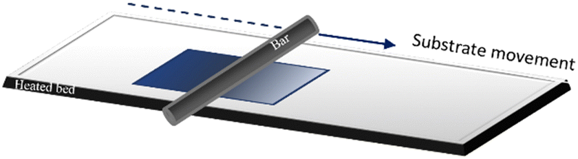 | ||
| Fig. 7 Schematic representation of the BAMS setup. | ||
Considering the previously reported OFET characteristics by Takimiya et al.,56 the solution-processed top contact C7-BTBT-C7 exhibits a mobility of more than 0.5 cm2 V−1 s−1. First, we attempted to fabricate bottom gate/bottom contact OFETs. Gold electrodes were designed and fabricated by photolithography on the silicon substrates. Then, solutions of C7-BTBT-C7 in chlorobenzene were deposited at 105 °C and at speeds of 1 mm s−1 and 10 mm s−1. Homogeneous films with a dragging speed of 10 mm s−1 were obtained. However, due to high contact resistance issues, and as previously reported by Li et al.40 for C8-BTBT-C8, it was not possible to record the transfer and output characteristics with this device configuration (Fig. S10, ESI†). We thus fabricated bottom gate/top contact OFETs on previously deposited thin films on Si/SiO2 substrates deposited (see the Experimental section).
In the view of previous works on C8-BTBT-C8 in which higher mobility OFETs were achieved when using blends of the organic semiconductor with polystyrene (PS),40,57 we also fabricated devices with C7-BTBT-C7![[thin space (1/6-em)]](https://www.rsc.org/images/entities/char_2009.gif) :PS blends 4:1 (with the PS of molecular weights 10000 g mol−1 and 280000 g mol−1). Typically, the device performance is expected to increase with the addition of the PS binder during deposition, there is a vertical phase separation, where PS remains on the bottom, and the organic semiconductor crystallizes on the top. This results in a reduction of the interfacial charge trap density and an enhancement of the device stability.58,59
:PS blends 4:1 (with the PS of molecular weights 10000 g mol−1 and 280000 g mol−1). Typically, the device performance is expected to increase with the addition of the PS binder during deposition, there is a vertical phase separation, where PS remains on the bottom, and the organic semiconductor crystallizes on the top. This results in a reduction of the interfacial charge trap density and an enhancement of the device stability.58,59
The films were then characterized by polarised optical microscopy (POM) to evaluate the morphology and crystallinity. All the films were highly homogenous and isotropic, showing a similar polycrystalline morphology (Fig. S11 and S12a, ESI†). The atomic force microscopy (AFM) topography images shown in Fig. 8 also highlight those peculiar morphological features. The thicknesses of the pristine C7-BTBT-C7 films coated at 1 mm s−1 and 10 mm s−1 were found to be 93.26 ± 12 nm and 44.15 ± 2.3 nm, respectively, with root mean square roughness (Rrms) values of 60.23 ± 15.61 nm and 3.38 ± 0.74 nm. Furthermore, the blend of C7-BTBT-C7 with PS at 1 mm s−1 and that 10 mm s−1 were found to be 76.14 ± 3 nm and 35.41 ± 3.5 nm thick, respectively, with root mean square roughness (Rrms) values of 18.04 ± 11.8 nm and 13.55 ± 4.23 nm. The films were quite uniform in thickness, as expected from the POM images. However, some cracks were visualised at the nanoscale, which was generally more pronounced in the pristine films. Such cracks are detrimental to charge transport but should not impede the formation of percolation paths.
 | ||
| Fig. 8 AFM height image of bottom gate/top contact devices of (a) C7-BTBT-C7 and (b) C7-BTBT-C7:PS thin films deposited via BAMS at different shearing rates (1 mm s−1 and 10 mm s−1). The scale bar corresponds to 10 μm. | ||
The XRD pattern of all the films with and without PS is consistent with the presence of the known phase of C7-BTBT-C7 preferentially oriented with the (100) plane parallel to the substrate (Fig. S12b, ESI†).
The electrical characterization of all the bottom gate/top contact devices with C7-BTBT-C7, C7-BTBT-C7:PS10k, and C7-BTBT-C7:PS280k as active layers was carried out (Table S6, ESI†). Fig. 9 displays the transfer (in the saturation regime) and output characteristics (see also Fig. S13, ESI†). The OFETs based on the pristine film as an active layer exhibit an average saturation mobility (μ) of 0.19 ± 0.02 cm2 V−1 s−1 and a threshold voltage (Vth) of −21.6 ± 0.54 V. However, the addition of the PS binder with a molecular weight of 10000 g mol−1 (i.e., PS10k) resulted in the highest μ value of 1.4 ± 0.45 cm2 V−1 s−1 with a Vth of −32 ± 1.40 V, while for C7-BTBT-C7:PS280k a saturation μ of 0.39 ± 0.09 cm2 V−1 s−1 and a Vth of −33 ± 1.40 V were observed. It is evident that the addition of the PS binder polymer drastically increases the mobility values. In all the cases, a high Vth was observed, probably owing to problems of contact resistance, which is a common issue with OFETs based on BTBT derivatives due to the low-lying HOMO of this material.60 This is also reflected by the lower mobility values achieved when OFETs with shorter channel lengths are measured (Table S6, ESI†).
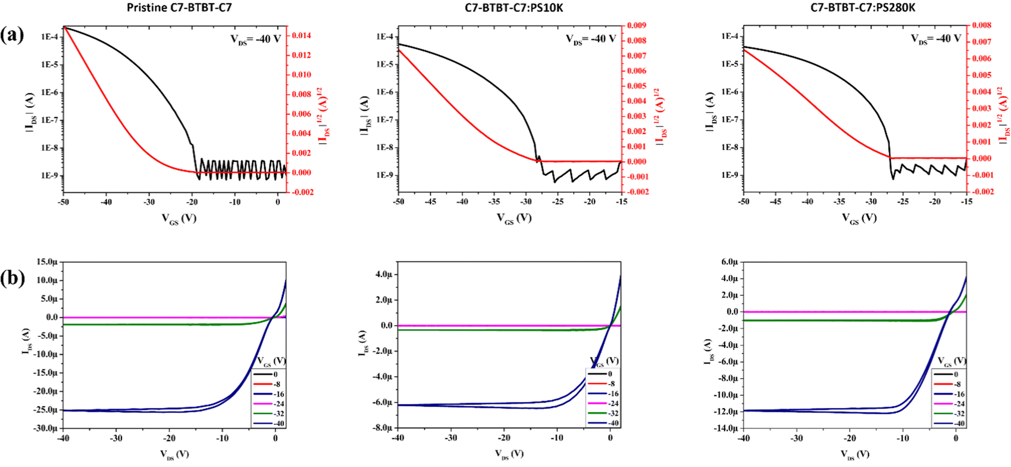 | ||
| Fig. 9 (a) Transfer and (b) output characteristics of pristine C7-BTBT-C7, C7-BTBT-C7:PS10k and C7-BTBT-C7:PS280k, showing saturation curves and output curves. Channel length: 200 μm and shearing speed: 10 mm s−1. | ||
Experimental section
Synthesis of C7-BTBT-C7
The synthesis of C7-BTBT-C7 was carried out according to a known procedure, starting from benzo[b]benzo[4,5]thieno[2,3-d]thiophene (BTBT).61,62Polymorph screening
The solubility screening of C7-BTBT-C7 was performed using 22 different solvents (Table S1, ESI†). Recrystallization from solvents at RT was performed in CHF, DCM, DEC, DMX, IPA, IPE, MEK, MPY, PXY, THF, and TOL. Meanwhile, recrystallization at 50 °C was carried out in ABZ, DMA, and DMF, and at 75 °C in 2PR and ETH. Anti-precipitation experiments from supersaturated solutions were performed with CHF:DMS (1:1), CHF:ETH (1:1), PXY:DMS (1:1), THF:2MX (1:1), THF:2PR (1:1), THF:can (1:1) and TOL:2MX (1:1). Controlled recrystallization with Crystal16 (Technobis, The Netherlands) was performed with 5 mg mL−1 solutions in DMA and DMF, and the solutions were heated until 100 °C and cooled at a constant rate of 0.125 °C min−1. In all the cases, the powder recovered was characterized by X-Ray powder diffraction, and the pattern was consistent with the known phase. C7-BTBT-C7 was also stable upon grinding, and no phase transition or amorphization was observed after the 5 minutes of neat manual grinding.
Powder X-ray diffraction (PXRD)
Qualitative PXRD to identify the crystalline form was collected at room temperature (25 °C) using a Rigaku MiniFlex 600 diffractometer with CuKα radiation from a copper-sealed tube operated at a 40 kV voltage and a 15 mA current using a Bragg–Brentano geometry. Diffraction patterns were measured over the 2θ range of 2–40° by step scanning with an increment of 0.01° per step.Thin film X-Ray diffraction
The XRD of C7-BTBT-C7 films was also carried out at room temperature (25 °C) with CuKα radiation.The films prepared by directional crystallization were collected at room temperature (25 °C) using a Panalytical diffractometer with 2D area detectors-PIXcel3D using parallel beam geometry in the 2θ range between 2° and 40° with an increment of 0.02° per step.
The XRD of C7-BTBT-C7 devices prepared using the BAMS shearing technique was performed at room temperature (25 °C) using a D-5000 model Siemens diffractometer with a secondary monochromator and a scintillation detector.
Single crystal X-ray diffraction (SCXRD)
The suitable crystals of C7-BTBT-C7 for SCXRD were obtained from CHF, DMA, and PXY solutions (1 mg ml−1). The crystal structure was collected at room temperature (25 °C) using an Oxford Diffraction Xcalibur S diffractometer with Mo Kα radiation (λ = 0.71073 Å) and a graphite monochromator. The data collection was performed at room temperature. The crystal structure was solved using WingX software-SHELXT codes and refined with SHELXL (version 2018/3). For the visualization of the crystal structure, CCDC Mercury 2020.3.0 was used.63,64 The R-factor (R1) was found to be 0.081, and the wR2 value (all data) was 0.152.Hirshfeld surface analysis
The CrystalExplorer 17.5 package was used for the Hirshfeld surface analysis, which was carried out based on the crystal geometry. The corresponding 2D fingerprint plots were also generated using CrystalExplorer 17.5 in the dnorm range of 0.0033 to 1.4654.Thermo-gravimetric analysis-evolved gas analysis (TGA-EGA)
The TGA-EGA was performed to determine the thermal stability and obtain information about the purity of the C7-BTBT-C7 powder. The measurement was performed in around 6 mg of the sample using a Mettler-Toledo TGA coupled with a Thermo Nicolet iS 10IR FT-IR spectrometer operated at a scan rate of 10 °C min−1 and analyzed using the STARe software.Differential scanning calorimetry (DSC)
The DSC of all the samples was performed using a Mettler-Toledo DSC1 instrument. About 2–4 mg of samples were crimped in hermetic aluminium crucibles (40 μL) and scanned from room temperature to 200 °C at a heating/cooling rate of 5 °C min−1 under a dry N2 atmosphere (a flow rate of 80 mL min−1). The data were processed using the STARe software.In situ variable temperature X-ray diffraction (VTXRD)
VTXRD was performed at Paul Scherrer Institut (PSI) Synchrotron radiation facility (Switzerland). PXRD in the capillary transmission mode at MS-X04SA beamline from 24 °C to 120 °C for C7-BTBT-C7. A beam energy of 12.4 keV (1.0 Å) was used for the data collection. The MS powder diffractometer is operated in Debye–Scherrer geometry, equipped with a solid-state silicon microstrip detector called the MYTHEN Microstrip sYstem for Time rEsolved experimeNts was utilized. Starting from room temperature, the XRD pattern was collected at various intervals until the complete conversion of the crystal to the liquid crystal for C7-BTBT-C7 (113 °C).65Hot stage microscopy (HSM)
Crystals on a glass-slide and covered with a cover slip were placed in a heating chamber (hot stage) using an OLYMPUS BX41 stereomicroscope equipped with a LINKAM LTS350 platinum plate for temperature control and a VISICAM analyzer. The heating chamber was capped with a sealable lid during heating and cooling cycles, and the rate was kept constant at 10 °C min−1. Time-lapse images were taken using a NIKON DS FI3 high-speed camera for all in situ experiments, and the images were analyzed using software Nikon NIS Elements and Linksys32 data capture.Ionization energy (IE)
Photoelectron yield spectroscopy (PYS) in air was used to determine IE values from the photoelectron emission yield of OSC samples in the form of powder. Photoelectron yield curves were collected within an energy range of 3.4 to 6.2 eV using a Riken Keiki spectrophotometer (Japan) model AC-2 with an energy step of 0.05 eV and a UV spot intensity of 25 nW. The final estimate for IE values is known with an experimental error of ±0.05 eV or less.Transfer integrals
The transfer integrals in the herringbone plane were computed using the ADF package within a fragmented approach,53 using the B3LYP functional and a DZ basis set. In our approach to compute the transfer integrals, the phase of our atomic orbitals is chosen arbitrarily. We evaluated the transfer integral signs by checking the phase consistency of the 2s atomic orbital coefficients by relying on the fact that the orbitals of equivalent monomers (i.e., in P pairs) must have the same phase (++ or −−) by translational symmetry. This helps us to deduce in the second stage the phase of the HOMOs in transverse pairs (T1 and T2). Note that due to the centrosymmetry of the unit cell, JT1 and JT2 systematically have the same sign. Reorganization energies were computed using the 4-point approach using the same level of theory.47,48Temperature gradient apparatus
The setup shown in Fig. 6(a) consists of a Linkam GS350 system presenting two distinct heating stages separated by a gap. One heating stage was set at a temperature above the melting point (Th), and the other was below the crystallization point (Tc) of C7-BTBT-C7. The distance (gap) between the two stages, where the thermal gradient was generated, is 2 mm. A 76 mm × 26 mm × 1 mm microscope glass slide (Marienfeld Cat. no. 1000000) was intercalated between the stages and the sample to ensure a constant displacement velocity of the sample. During our thermal gradient experiments for C7-BTBT-C7, the hot stage was set at a temperature Th of 160 °C, while the cold stage was maintained at a temperature Tc of 70 °C or 90 °C. The setup is closed using a hermetic lid, so the system remains thermally independent of the laboratory environment. The stage was mounted on a polarized optical microscope (POM) Nikkon Eclipse80i to take images before, during, and after the experiment.
000.55 A FKM solution was prepared in acetone (60 mg mL−1) and kept on overnight stirring at 1000 rpm. The solution was then filtered using a 5 μm phobic filter. This FKM solution was then spin-coated at various FKM (μL) amounts and spin-coating speeds with a constant acceleration of 4000 s on glass substrates cleaned according to the previously described procedure.
Calibration of the magnitude of the temperature gradient setup (Gcal)
Previous work has shown that the effective magnitude of the temperature gradient (Gexp) that takes place between the hot and cold zones is less than the magnitude calculated by the equation G = (Th − Tc)/x, where x = 2.0 mm (the gap between the hot and cold stages).29 For our experiments, the temperature gradient was calculated to be Gexp ≈ 45 °C mm−1 and Gexp ≈ 35 °C mm−1 for the Th–Tc couples at 160–70 °C and 160–90 °C, respectively.28Thin-film polymorph screening
Films of C7-BTBT-C7 were prepared by solution processing on silicon substrates by varying several parameters like solvents (chloroform, p-xylene, and chlorobenzene), processing techniques (spin-coating, drop casting, and shear coating), temperatures (pre- and post-thermal treatment up to 115 °C) and concentrations (1 mg mL−1, 3 mg mL−1, and 22.6 mg mL−1 (2%)). All the fabricated films exhibit the bulk crystal form observed by X-ray diffraction.Transistor fabrication and characterization
(1) Bottom gate/bottom contact devices: the Si/SiO2 substrates with a SiO2 thickness of 200 nm, C = 17.26 nF cm−2, with interdigitated electrodes made by photolithography were fabricated consisting of Cr (5 nm) and gold (40 nm), deposited by thermal evaporation at deposition rates of 0.1–0.5 Å s−1 and 1–5 Å s−1, respectively (Micro-Writer ML3 from Durham Magneto Optics). The channel lengths for the bottom gate/bottom contact were 100 and 150 μm, and the channel width/length ratio was always set to 100. The substrates were sonicated in acetone and isopropanol for 15 minutes, followed by 25 minutes of UV-Ozone treatment to avoid dewetting. These substrates were immersed in a 15 mM solution of penta-fluorobenzenethiol (PFBT) in isopropanol for 15 minutes to modify the work function of Au contacts. PFBT was purchased from Sigma-Aldrich. Finally, the substrates were rinsed with pure isopropanol and dried under a nitrogen flow.(2) Bottom gate/top contact devices: the silicon substrates were cleaned with acetone and isopropanol, as mentioned above. After solution shearing deposition, the films were mounted on the stage with shadow masks with a channel width W of 4000 μm and channel lengths L of 50–200 μm. The stage was carefully placed in the thermal evaporator, and the chamber was kept under vacuum for 3 hours using a Leynold screen operator. After 3 hours, the Au-deposition was started. The program was set at an Au-thickness of 25 nm. After evaporation, the samples were kept in the dark for 7 days.
(3) Organic semiconductor solution deposition: the pristine ink consisted of 2 wt% solutions of C7-BTBT-C7 in chlorobenzene, which was dissolved by heating overnight at 105 °C. Polystyrene Mw = 10000 (10k) and 280000 (280k) g mol−1 were purchased from Sigma-Aldrich and used without further purification. A blend solution of C7-BTBT-C7 and PS in chlorobenzene 2 wt% was prepared at a weight ratio C7-BTBT-C7:PS 4:1. Both the pristine and blend films were deposited using the BAMS technique under ambient conditions at 105 °C and at coating speeds of 10 and 1 mm s−1, as previously reported.40
(4) Electrical measurements: transistor measurements were carried out using an Agilent B1500A semiconductor device analyzer under ambient conditions. For all transfer measurements, the VDS values were −5 V (linear) and −40 V (saturation). The devices were characterized by extracting the field-effect mobility in the saturation regime and the threshold voltage (Vth). μ was extracted using the following equation:

Morphological characterization of the OFETs
Optical microscopy pictures were taken using an Olympus BX51 equipped with a polarizer analyzer. AFM images were obtained using a Park NX10 system using PPP-NCHR tips in non-contact mode and applying the adaptive scan rate to slow down the scan speed at crystallite borders. Subsequent data analysis was performed using the Gwyddion software.Conclusions
In summary, we have conducted an exhaustive study of the C7-BTBT-C7 molecule from synthesis to device fabrication. We have provided evidence for the critical role of structural factors that can influence electronic properties. We examined polymorphism that plays a key role as it is advantageous for tuning electronic properties. Therefore, we screened the bulk and the thin-film polymorphism along with different methods to control the formation of polymorphs using non-equilibrium techniques. From all these comprehensive polymorph screening experiments (both conventional and non-conventional), we identified only one crystal form, which transforms into a liquid crystal at 107 °C. Focusing on the structural parameters and odd–even effects, we discovered that C7-BTBT-C7 is isomorphous with C8 and C12 BTBTs. In our research, we placed our emphasis on the descriptors of packing parameters, and we concluded that longer chains tighten the packing, corroborating the previous results with even chain lengths.46 The structural similarity of the three systems also agrees with the ionization energies and the transfer integrals. Despite the small structural changes observed in the herringbone direction, the transfer integrals are comparable with similar trends.Later, we fabricated devices using the solution shearing technique. The electrical characterization of all the bottom gate/top contact devices with C7-BTBT-C7 and C7-BTBT-C7 with the PS binder polymer of different molecular weights (10000 and 280000 g mol−1) was carried out. The results demonstrate that C7-BTBT-C7:PS10k exhibits the highest mobility of 1.4 ± 0.45 cm2 V−1 s−1. The consistent stability of one crystal phase in the bulk and thin films turns out to be advantageous for a stable device. The high mobility, together with the simple processing technique, qualifies this OSC to be a good candidate for electronic applications.
Author contributions
P. P.: investigation of the bulk and thin film polymorph screening for all the techniques, OFET fabrication, and manuscript writing. L. F.: contribution to OFET fabrication and analysis. N. M., M. B., and S. G.: computing the transfer integrals and coupling–sign relationship. N. T.: measurement of ionization energies and AFM analysis. C. R.: the synthesis of C7-BTBT-C7. G. S.: conceptualization for directional crystallization and editing the manuscript. D. B. J. C., P. S., M. M. T., Y. H. G., E. M., and L. M.: supervision and manuscript review and editing.Conflicts of interest
There are no conflicts to declare.Acknowledgements
We acknowledge the Paul Scherrer Institut, Villigen, Switzerland, for the provision of synchrotron radiation beam time at the beamline MS-X04SA of the SLS (ID proposal 20201790). P. P., L. F., N. M., N. T., J. C., P. S., M. M. T., Y. G., E. M., and L. M., contributors of the paper, are the members of the UHMob project. This work has received funding from the European Union's Horizon 2020 research and innovation program under the Marie Sklodowska-Curie grant no. 811284. G. S. is a FNRS Research Associate (Belgian National Fund for Scientific Research). G. S. acknowledges financial support from the Francqui Foundation (Francqui Start-Up Grant). G. S. thanks the FNRS for financial support through the research project COHERENCE2 (no. F.4536.23). M. M. T. and L. F. also acknowledge MCIN through the project GENESIS PID2019 and the “Severo Ochoa” Programme for Centers of Excellence in R&D (FUNFUTURE CEX2019-000917-S), and the Generalitat de Catalunya (2017-SGR-918).Notes and references
- H. Sirringhaus, Adv. Mater., 2014, 26, 1319–1335 CrossRef CAS PubMed.
- K. Takimiya, M. Nakano, H. Sugino and I. Osaka, Synth. Met., 2016, 217, 68–78 CrossRef CAS.
- Y. Tsutsui, G. Schweicher, B. Chattopadhyay, T. Sakurai, J. B. Arlin, C. Ruzié, A. Aliev, A. Ciesielski, S. Colella, A. R. Kennedy, V. Lemaur, Y. Olivier, R. Hadji, L. Sanguinet, F. Castet, S. Osella, D. Dudenko, D. Beljonne, J. Cornil, P. Samorì, S. Seki and Y. H. Geerts, Adv. Mater., 2016, 28, 7106–7114 CrossRef CAS PubMed.
- G. H. Roche, Y. T. Tsai, S. Clevers, D. Thuau, F. Castet, Y. H. Geerts, J. J. E. Moreau, G. Wantz and O. J. Dautel, J. Mater. Chem. C, 2016, 4, 6742–6749 RSC.
- E. Benvenuti, D. Gentili, F. Chiarella, A. Portone, M. Barra, M. Cecchini, C. Cappuccino, M. Zambianchi, S. G. Lopez, T. Salzillo, E. Venuti, A. Cassinese, D. Pisignano, L. Persano, M. Cavallini, L. Maini, M. Melucci, M. Muccini and S. Toffanin, J. Mater. Chem. C, 2018, 6, 5601–5608 RSC.
- M. Melucci, M. Durso, C. Bettini, M. Gazzano, L. Maini, S. Toffanin, S. Cavallini, M. Cavallini, D. Gentili, V. Biondo, G. Generali, F. Gallino, R. Capelli and M. Muccini, J. Mater. Chem. C, 2014, 2, 3448–3456 RSC.
- C. Cappuccino, P. P. Mazzeo, T. Salzillo, E. Venuti, A. Giunchi, R. G. Della Valle, A. Brillante, C. Bettini, M. Melucci and L. Maini, Phys. Chem. Chem. Phys., 2018, 20, 3630 RSC.
- L. Maini, F. Gallino, M. Zambianchi, M. Durso, M. Gazzano, K. Rubini, D. Gentili, I. Manet, M. Muccini, S. Toffanin, M. Cavallini and M. Melucci, Chem. Commun., 2015, 51, 2033–2035 RSC.
- C. Ruzié, J. Karpinska, A. Laurent, L. Sanguinet, S. Hunter, T. D. Anthopoulos, V. Lemaur, J. Cornil, A. R. Kennedy, O. Fenwick, P. Samorì, G. Schweicher, B. Chattopadhyay and Y. H. Geerts, J. Mater. Chem. C, 2016, 4, 4863–4879 RSC.
- K. Takimiya, S. Shinamura, I. Osaka and E. Miyazaki, Adv. Mater., 2011, 23, 4347–4370 CrossRef CAS PubMed.
- K. Takimiya, I. Osaka, T. Mori and M. Nakano, Acc. Chem. Res., 2014, 47, 1493–1502 CrossRef CAS PubMed.
- J. Bernstein, Polymorphism in Molecular Crystals, Clarendon Press, Oxford, 2002 Search PubMed.
- C. Cappuccino, L. Catalano, F. Marin, G. Dushaq, G. Raj, M. Rasras, R. Rezgui, M. Zambianchi, M. Melucci, P. Naumov and L. Maini, Cryst. Growth Des., 2020, 20, 884–891 CrossRef CAS.
- J. Bernstein, Cryst. Growth Des., 2011, 11, 632–650 CrossRef CAS.
- M. Mas-Torrent and C. Rovira, Chem. Rev., 2011, 111, 4833–4856 CrossRef CAS PubMed.
- S. Riera-Galindo, A. Tamayo and M. Mas-Torrent, ACS Omega, 2018, 3, 2329–2339 CrossRef CAS PubMed.
- P. Pandey, N. Demitri, L. Gigli, A. M. James, F. Devaux, Y. H. Geerts, E. Modena and L. Maini, Cryst. Growth Des., 2022, 22, 1680–1690 CrossRef CAS.
- C. Cappuccino, S. Canola, G. Montanari, S. G. Lopez, S. Toffanin, M. Melucci, F. Negri and L. Maini, Cryst. Growth Des., 2019, 19, 2594–2603 CrossRef CAS.
- I. de Oliveira Martins, F. Marin, E. Modena and L. Maini, Faraday Discuss., 2022, 235, 490–507 RSC.
- O. D. Jurchescu, D. A. Mourey, S. Subramanian, S. R. Parkin, B. M. Vogel, J. E. Anthony, T. N. Jackson and D. J. Gundlach, Phys. Rev. B: Condens. Matter Mater. Phys., 2009, 80, 85201 CrossRef.
- T. Salzillo and A. Brillante, Adv. Mater. Interfaces, 2022, 9, 2200815 CrossRef CAS.
- A. O. F. Jones, B. Chattopadhyay, Y. H. Geerts and R. Resel, Adv. Funct. Mater., 2016, 26, 2233–2255 CrossRef CAS.
- S. Schiefer, M. Huth, A. Dobrinevski and B. Nickel, J. Am. Chem. Soc., 2007, 129, 10316–10317 CrossRef CAS PubMed.
- G. Schweicher, Y. Olivier, V. Lemaur and Y. H. Geerts, Isr. J. Chem., 2014, 54, 595–620 CrossRef CAS.
- L. Merces, R. F. de Oliveira, H. L. Gomes and C. C. Bof Bufon, Org. Electron., 2017, C, 107–113 CrossRef.
- Y. Diao, L. Shaw, Z. Bao and S. C. B. Mannsfeld, Energy Environ. Sci., 2014, 7, 2145–2159 RSC.
- Y. Xia, R. Li, E. Tsai, Y. He, T. Liu, X. Zhao, K. Gu, H. Meng and Y. L. Loo, Adv. Electron. Mater., 2021, 7, 2000792 CrossRef CAS.
- G. Schweicher, G. Liu, P. Fastré, R. Resel, M. Abbas, G. Wantz and Y. H. Geerts, Mater. Chem. Front., 2021, 5, 249–258 RSC.
- P. Panini, B. Chattopadhyay, O. Werzer and Y. Geerts, Cryst. Growth Des., 2018, 18, 2681–2689 CrossRef CAS.
- F. G. Del Pozo, S. Fabiano, R. Pfattner, S. Georgakopoulos, S. Galindo, X. Liu, S. Braun, M. Fahlman, J. Veciana, C. Rovira, X. Crispin, M. Berggren and M. Mas-Torrent, Adv. Funct. Mater., 2016, 26, 2379–2386 CrossRef CAS.
- I. Temiño, F. G. Del Pozo, M. R. Ajayakumar, S. Galindo, J. Puigdollers and M. Mas-Torrent, Adv. Mater. Technol., 2016, 1, 1600090 CrossRef.
- T. Salzillo, N. Montes, R. Pfattner and M. Mas-Torrent, J. Mater. Chem. C, 2020, 8, 15361–15367 RSC.
- T. Salzillo, A. Campos, A. Babuji, R. Santiago, S. T. Bromley, C. Ocal, E. Barrena, R. Jouclas, C. Ruzie, G. Schweicher, Y. H. Geerts and M. Mas-Torrent, Adv. Funct. Mater., 2020, 30, 2006115 CrossRef CAS.
- A. Tamayo, S. Riera-Galindo, A. O. F. Jones, R. Resel and M. Mas-Torrent, Adv. Mater. Interfaces, 2019, 6, 1900950 CrossRef CAS.
- S. Galindo, A. Tamayo, F. Leonardi and M. Mas-Torrent, Adv. Funct. Mater., 2017, 27, 1700526 CrossRef.
- S. Colella, C. Ruzié, G. Schweicher, J. B. Arlin, J. Karpinska, Y. Geerts and P. Samorì, ChemPlusChem, 2014, 79, 371–374 CrossRef CAS PubMed.
- H. Ebata, T. Izawa, E. Miyazaki, K. Takimiya, M. Ikeda, H. Kuwabara and T. Yui, J. Am. Chem. Soc., 2007, 129, 15732–15733 CrossRef CAS PubMed.
- S. Kwon, J. Kim, G. Kim, K. Yu, Y. R. Jo, B. J. Kim, J. Kim, H. Kang, B. Park and K. Lee, Adv. Mater., 2015, 27, 6870–6877 CrossRef CAS PubMed.
- M. M. Torrent and C. Rovira, Chem. Soc. Rev., 2008, 37, 827–838 RSC.
- J. Li, A. Babuji, I. Temiño, T. Salzillo, F. D’Amico, R. Pfattner, C. Ocal, E. Barrena and M. Mas-Torrent, Adv. Mater. Technol., 2022, 7, 2101535 CrossRef CAS.
- H. Minemawari, T. Yamada, H. Matsui, J. Tsutsumi, S. Haas, R. Chiba, R. Kumai and T. Hasegawa, Nature, 2011, 475, 364–367 CrossRef CAS PubMed.
- H. B. Akkerman, S. C. B. Mannsfeld, A. P. Kaushik, E. Verploegen, L. Burnier, A. P. Zoombelt, J. D. Saathoff, S. Hong, S. Atahan-Evrenk, X. Liu, A. Aspuru-Guzik, M. F. Toney, P. Clancy and Z. Bao, J. Am. Chem. Soc., 2013, 135, 11006–11014 CrossRef CAS PubMed.
- G. H. Roche, G. Bruckner, D. G. Dumitrescu, J. J. E. Moreau, A. V. D. Arie Van Der Lee, G. Wantz and O. J. Dautel, Adv. Electron. Mater., 2022, 8(1), 2100265 CrossRef CAS.
- S. Sergeyev, W. Pisula and Y. H. Geerts, Chem. Soc. Rev., 2007, 36, 1902–1929 RSC.
- C. Grigoriadis, C. Niebel, C. Ruzié, Y. H. Geerts and G. Floudas, J. Phys. Chem. B, 2014, 118, 1443–1451 CrossRef CAS PubMed.
- T. Izawa, E. Miyazaki, K. Takimiya, K. Takimiya, T. Izawa and E. Miyazaki, Adv. Mater., 2008, 20, 3388–3392 CrossRef CAS.
- V. Coropceanu, J. Cornil, D. A. da Silva Filho, Y. Olivier, R. Silbey and J. L. Brédas, Chem. Rev., 2007, 107, 926–952 CrossRef CAS PubMed.
- H. Oberhofer, K. Reuter and J. Blumberger, Chem. Rev., 2017, 117, 10319–10357 CrossRef CAS PubMed.
- G. Schweicher, G. D’Avino, M. T. Ruggiero, D. J. Harkin, K. Broch, D. Venkateshvaran, G. Liu, A. Richard, C. Ruzié, J. Armstrong, A. R. Kennedy, K. Shankland, K. Takimiya, Y. H. Geerts, J. A. Zeitler, S. Fratini and H. Sirringhaus, Adv. Mater., 2019, 31, 1902407 CrossRef CAS PubMed.
- T. F. Harrelson, V. Dantanarayana, X. Xie, C. Koshnick, D. Nai, R. Fair, S. A. Nuñez, A. K. Thomas, T. L. Murrey, M. A. Hickner, J. K. Grey, J. E. Anthony, E. D. Gomez, A. Troisi, R. Faller and A. J. Moulé, Mater. Horiz., 2019, 6, 182–191 RSC.
- S. Fratini, S. Ciuchi, D. Mayou, G. T. de Laissardière and A. Troisi, Nat. Mater., 2017, 16, 998–1002 CrossRef CAS PubMed.
- S. Fratini, D. Mayou and S. Ciuchi, Adv. Funct. Mater., 2016, 26, 2292–2315 CrossRef CAS.
- S. Giannini and J. Blumberger, Acc. Chem. Res., 2022, 55, 819–830 CrossRef CAS PubMed.
- S. S. Lee, S. B. Tang, D. M. Smilgies, A. R. Woll, M. A. Loth, J. M. Mativetsky, J. E. Anthony and Y. L. Loo, Adv. Mater., 2012, 24, 2692–2698 CrossRef CAS PubMed.
- V. De Cupere, J. Tant, P. Viville, R. Lazzaroni, W. Osikowicz, W. R. Salaneck and Y. H. Geerts, Langmuir, 2006, 22, 7798–7806 CrossRef CAS PubMed.
- K. Takimiya, T. Yamamoto, H. Ebata and T. Izawa, Thin Solid Films, 2014, 554, 13–18 CrossRef CAS.
- I. Temiño, F. G. Del Pozo, M. R. Ajayakumar, S. Galindo, J. Puigdollers and M. Mas-Torrent, Adv. Mater. Technol., 2016, 1, 1600090 CrossRef.
- L. Fijahi, T. Salzillo, A. N. Tamayo, M. Bardini, C. Ruzié, C. Quarti, D. Beljonne, S. D’agostino, Y. H. Geerts and M. Mas-Torrent, J. Mater. Chem. C, 2022, 10, 7319–7328 RSC.
- A. Campos, S. Riera-Galindo, J. Puigdollers and M. Mas-Torrent, ACS Appl. Mater. Interfaces, 2018, 10, 15952–15961 CrossRef CAS PubMed.
- Y. Shi, J. Liu, Y. Hu, W. Hu and L. Jiang, Nano Sel., 2021, 2, 1661–1681 CrossRef CAS.
- B. Košata, V. Kozmik, J. Svoboda, V. Novotná, P. Vaněk and M. Glogarová, Liq. Cryst., 2003, 30, 603–610 CrossRef.
- H. Ebata, T. Izawa, E. Miyazaki, K. Takimiya, M. Ikeda, H. Kuwabara and T. Yui, J. Am. Chem. Soc., 2007, 129, 15732–15733 CrossRef CAS PubMed.
- C. F. MacRae, I. Sovago, S. J. Cottrell, P. T. A. Galek, P. McCabe, E. Pidcock, M. Platings, G. P. Shields, J. S. Stevens, M. Towler and P. A. Wood, J. Appl. Crystallogr., 2020, 53, 226–235 CrossRef CAS PubMed.
- C. F. Macrae, I. J. Bruno, J. A. Chisholm, P. R. Edgington, P. McCabe, E. Pidcock, L. Rodriguez-Monge, R. Taylor, J. Van De Streek and P. A. Wood, J. Appl. Crystallogr., 2008, 41, 466–470 CrossRef CAS.
- P. R. Willmott, D. Meister, S. J. Leake, M. Lange, A. Bergamaschi, M. Böge, M. Calvi, C. Cancellieri, N. Casati, A. Cervellino, Q. Chen, C. David, U. Flechsig, F. Gozzo, B. Henrich, S. Jäggi-Spielmann, B. Jakob, I. Kalichava, P. Karvinen, J. Krempasky, A. Lüdeke, R. Lüscher, S. Maag, C. Quitmann, M. L. Reinle-Schmitt, T. Schmidt, B. Schmitt, A. Streun, I. Vartiainen, M. Vitins, X. Wang and R. Wullschleger, J. Synchrotron Radiat., 2013, 20, 667–682 CrossRef CAS PubMed.
Footnote |
| † Electronic supplementary information (ESI) available. CCDC 2225078. For ESI and crystallographic data in CIF or other electronic format see DOI: https://doi.org/10.1039/d3tc00434a |
| This journal is © The Royal Society of Chemistry 2023 |