
 Open Access Article
 This Open Access Article is licensed under a
 Creative Commons Attribution 3.0 Unported Licence
Multi-pulse atomic layer deposition of p-type SnO thin films: growth processes and the effect on TFT performance†
Daisy E.
Gomersall
 *a,
Kham M.
Niang
a,
James D.
Parish
b,
Zhuotong
Sun
c,
Andrew L.
Johnson
b,
Judith L.
MacManus-Driscoll
c and
Andrew J.
Flewitt
a
*a,
Kham M.
Niang
a,
James D.
Parish
b,
Zhuotong
Sun
c,
Andrew L.
Johnson
b,
Judith L.
MacManus-Driscoll
c and
Andrew J.
Flewitt
a
aElectrical Engineering Division, Engineering Department, University of Cambridge, Cambridge CB3 0FA, UK. E-mail: daisy.gomersall@cantab.net
bDepartment of Chemistry, University of Bath, Claverton Down, Bath, BA2 7AY, UK
cDepartment of Materials Science & Metallurgy, University of Cambridge, Cambridge CB3 0FS, UK
First published on 13th April 2023
Abstract
This work demonstrates p-type SnO thin film transistors, where the SnO active layers were deposited with atomic layer deposition (ALD) using the Sn(II) alkoxide precursor, Sn(II) bis(tert-butoxide). The deposition optimisation explores the use of multiple Sn pulses per ALD cycle and the use of an exposure mode (where the pump extraction is paused before the Sn precursor purge) to increase the residence time and allow for more effective saturation of the surface. The fabricated devices required post deposition annealing of the active layer, with device performance further improved by back-channel passivation using ALD Al2O3. The performance of devices deposited using the varying precursor delivery modes has also been compared, with the devices utilizing deposition with multiple Sn pulses and a post deposition anneal at 250 °C achieving an on/off ratio of ∼4 × 10⁴ and field effect mobility (μFE) of 0.6 cm2 (V s)−1. The growth processes present during deposition with the different precursor delivery modes was investigated using fractal geometry and topographical scaling methods, with the poor device performance for the single Sn pulse deposition attributed to 2D lateral island growth.
1 Introduction
Tin monoxide (SnO) has emerged as one of the most promising metal oxide materials from which to fabricate p-type thin film transistors (TFTs)1,2 and complementary metal oxide semiconductor (CMOS) circuits in conjunction with n-channel TFTs.3–5 It has a band gap in the range 2.7–3.4 eV,1,2,6 but unlike most metal oxide materials, where the valence band maximum (VBM) is dominated by O 2p orbitals leading to poor hole mobility and poor p-type conduction, the VBM in SnO is dominated by contributions from both Sn 5s and O 2p orbitals, providing a relatively high hole mobility.7 One consistent difficulty associated with the use of SnO is that it is metastable and readily oxidises to SnO2.8 Moreover, it has been shown that the incorporation of metallic Sn within sputtered SnO films can lead to a higher mobility phase,9,10 with reported values of Hall mobility reaching 18.7 cm2 (V s)−1.9P-type TFTs have been successfully fabricated using sputtering,9–12 thermal evaporation,13 solution processing14 and pulsed laser deposition.15 Although achieving field effect mobilities of ∼1 cm2 (V s)−1, typically these have all exhibited low on/off ratios (102–104), which is undesirable for CMOS logic circuits as it results in increased static power consumption.5 However, p-type devices fabricated by Kim et al.16 using atomic layer deposition (ALD) demonstrate a high on/off ratio of 2 × 10⁶, subthreshold swing (SS) of 1.8 V dec−1 and field effect mobility (μFE) of ∼1 cm2 (V s)−1.
This work reports the atomic layer deposition (ALD) of SnO films and the successful fabrication of p-type metal oxide TFTs, using Sn(II) bis(tert-butoxide) (Sn(OtBu)2). The reaction mechanism for the formation of SnO by ALD can be written using two separate half-reactions, as follows:
| SnO–OH* + Sn(OtBu)2 → SnO–O–Sn–OtBu* + HOtBu(A) |
| SnO–O–Sn–OtBu* + H2O → SnO–Sn–OH* + HOtBu(B) |
To-date only a limited number of precursors for the ALD of SnO have been described,17,18 with fewer capable of depositing films with desirable p-type properties. Of these, the most notable is the tin(II) aminoalkoxide complex, Sn(dmamp)2, which was used in particular for the ALD of high performing p-type SnO by Kim et al.16 In contrast to the four-coordinate Sn(dmamp)2, Sn(OtBu)2, which has previously been employed in the chemical vapour deposition of SnO, utilises simple non-chelating alkoxide ligands in an attempt to alter the reactivity and ALD behaviour of the complex.19 Similar work by Mameli et al.20 has recently described the use of an analogous simple Sn(II) alkoxide complex Sn(II) (tert-amyloxide) in the high-throughput spatial ALD of p-type SnO. A comparison of evaporation rates for Sn(II) bis(tert-butoxide) (Sn(OtBu)2) and Sn(dmamp)2, obtained from isothermal thermogravimetric analysis (TGA) experiments show that the evaporation rates (i.e. volatilities) are slightly higher for Sn(OtBu)2 (128.4 μg min−1 cm−2 at 70 °C) compared to Sn(dmamp)2 (118.7 μg min−1 cm−2 at 70 °C). However, with the style of vapour-draw ALD system used in this work and with the Sn(OtBu)2 heated to 100 °C, there was no measurable increase in the reactor chamber pressure during the Sn precursor pulse. Therefore, to ensure a high dosage of precursor into the reactor chamber, work reported herein explores the use of multiple Sn precursor pulses and an exposure mode to increase the precursor dose per cycle.
P-type SnO devices were fabricated and the effect of post deposition vacuum annealing and device passivation by ALD Al2O3 has been demonstrated alongside a comparison of the performance of three different precursor delivery modes. AFM and fractal analysis of the film surface identifies the presence of lateral island growth when only 1 Sn pulse is used. This explains the improved device performance when multiple Sn pulses are used and in addition to the insight offered for this specific precursor, it suggests an approach that could be adapted for similar low volatility ALD precursors.
2 Experimental details
SnO films were deposited using a Cambridge Nanotech Savannah ALD 100 system, where the Sn(II) bis-(tert-butoxide) (heated to 100 °C) and H2O were delivered by a vapour draw system.21Fig. 1 shows a comparative schematic for three different protocols for the Sn precursor pulse and purge: (a) a single 1 s pulse of Sn precursor followed by a 15 s purge; (b) three 1 s pulses of Sn precursor separated by a wait of 5 s and followed by a 10 s purge; and (c) three 1 s pulses of Sn precursor separated by a wait of 5 s, followed by a 5 s stop of the flow by shutting the valve on the vacuum line, used to increase the precursor residence time in the chamber and referred to here as the exposure mode of deposition (increased substrate exposure to the precursor), and finally a 10 s purge. In (b) and (c) the chamber is continuously evacuated during both the “wait” and “purge” steps. A single ALD cycle consisted of the respective precursor pulse and purge followed by a 0.025 s H2O pulse and 10 s N2 purge. The N2 flow was set to 20 sccm throughout the deposition.
 | ||
| Fig. 1 Schematic of the deposition process, comparing the three Sn precursor pulse and purge protocols: (a) 1 x Sn pulse mode, (b) 3 x Sn pulse mode, (c) 3 x Sn pulse with exposure mode. | ||
Bottom gate p-type SnO TFTs were fabricated by depositing onto Si/SiO2 wafers, with the Si acting as a global back gate, SiO2 acting as the gate dielectric and evaporated Au providing the source/drain contacts (shown in Fig. 2). The SnO patterning was done by wet etch using dilute oxalic acid. Where stated, post deposition vacuum annealing of the SnO thin films was completed using a quartz tube heater (1 h at a pressure of 5 × 10⁻³ mBar) prior to Au contact patterning and evaporation, and the back channel was passivated with Al2O3 deposited at 150 °C using ALD. The thicknesses of the SnO thin films were modelled using spectroscopic ellipsometry (Accurion EP4 ellipsometer with wavelengths in the range 400–900 nm) and the Tauc–Lorentz model. The TFTs presented here have a SnO thickness of ∼30 nm for the 1 Sn pulse mode and 3 Sn pulse mode, and ∼25 nm for the 3 Sn pulse mode with exposure, channel length of 50 μm and a W/L ratio of 20. Electrical characterization was performed using an Agilent B1500A semiconductor parameter analyzer. Hall measurements were taken for samples with Au contacts in van der Pauw configuration at a magnetic field of 0.2 Tesla at room temperature (MMR Technologies Hall System).
 | ||
| Fig. 2 Device structure: (a) thin film transistor, (b) capacitor. | ||
The X-ray diffraction (XRD) data was taken on a Bruker D8 Davinci XRD system in the Bragg Brentano geometry and the atomic force microscope (AFM) images on a 5420 Agilent Technologies AFM in non-contact mode and tip radius of 8 nm; for both, the samples were deposited on glass substrates (Corning 7059). The AFM images were processed (levelled and denoised) using Gwyddion, but the scaling analysis completed using python. The chemical bonding states of the SnO thin film were investigated using X-ray photoelectron spectroscopy (XPS) using an Al kα 1 X-ray source (hν = 1486.6 eV) and a SOECS PHOIBOS 150 electron energy analyser. Ag paste was placed on the film edges to reduce charging and the O 1s peak was used for a relative binding energy calibration between films. The absorption coefficient has been calculated from transmission data measured using an ATI Unicam UV/Vis spectrometer over a wavelength range of 200–1100 nm, with the films deposited on quartz substrates (Spectrosil B polished windows).
All measurements were taken at ambient temperature and pressure, with all the electrical characterisation completed in the dark to remove photoconductivity and illumination effects. The samples were kept in a dessicator between measurements, where they remained stable over a period of months.
3 Results and discussion
3.1 Deposition optimisation
This section details the optimisation of the Sn precursor pulse length and substrate temperature by considering their effect on the growth per cycle (GPC).Fig. 3(a) shows the variation in GPC as the Sn pulse length is increased from 0.25 s to 3 s. As expected, at the smaller pulse lengths, the growth per cycle increases with increasing pulse length, but at a pulse length of 2 s the growth per cycle saturates. This is typical of ALD processes as the substrate surface reaches saturation and therefore higher pulse lengths can no longer impact the growth rate.22 However, at the longer pulse lengths of 2 s and 3 s, there was poor uniformity in the film thickness, seen in the larger error for the thickness measurement.
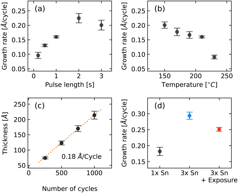 | ||
| Fig. 3 Optimisation of the ALD process: (a) growth per cycle (GPC) vs. pulse length for single pulse mode, with substrate temperature set to 210 °C for 500 cycles; (b) GPC vs. substrate temperature for single pulse mode, with pulse length 1 s for 500 cycles; (c) thickness vs. number of cycles with a linear regression and extracted GPC, for single pulse mode with 1 s pulse length and substrate temperature 170 °C; and (d) GPC vs. mode of precursor delivery and purge, with pulse length 1 s and substrate temperature 170 °C for 500 cycles in the 1 x Sn and 3 x Sn modes and 1000 cycles for the exposure mode. | ||
Fig. 3(b) shows that the GPC decreases as the substrate temperature is increased from 150 °C to 230 °C, with a pulse length of 1 s. This is a tendency regularly seen in ALD processes23 and has previously been reported for the deposition of SnO22,24,25 and ZnO26 using H2O as a reactant, with the decrease in GPC likely due to a reduction in OH absorption density on the growing surface as the temperature increases.22,27
The thickness per number of cycles is shown in Fig. 3(c), with pulse length 1 s, temperature 170 °C. The growth per cycle of 0.18 Å per cycle is calculated using a linear regression (dashed line) of the data for 500 cycles and above. The point at 250 cycles has been excluded as it distorts the linear fit, suggesting the deposition is demonstrating accelerated growth where the nucleation and initial growth is faster than later during the deposition.28
Fig. 3(d) shows the comparison in the growth per cycle for three different modes for the precursor delivery and purge. The two additional precursor delivery modes were explored due to the fact that the as-deposited films deposited with a single pulse of Sn precursor were very resistive, requiring a post deposition anneal at 350 °C to reach measurable currents, and the XRD data (provided in Fig. 4) had no distinct peaks corresponding to SnO. Niang et al. have previously shown an improvement in the Raman peak intensity of VO2 films by exploring the use of multiple pulses of the Vanadium precursor.29 This method of multiple pulses has also been shown to increase the growth rate per cycle of TiO230 and in work by Aria et al. to increase the homogeneity of surface nucleation when depositing AlOx on graphene.31 In addition to multiple pulses, Aria et al. showed that this uniformity of nucleation was improved further by depositing the films in stop-flow mode (referred to as exposure mode in this work) where the pump is stopped immediately after the precursor pulse, to create a static atmosphere for a time (thold), which provides a saturation period for the precursor on the substrate surface.
 | ||
| Fig. 4 XRD patterns for as-deposited SnO films, comparing the three modes of precursor delivery and purge. | ||
Both of these methods effectively increase the precursor dose per cycle. As the Savannah ALD![[thin space (1/6-em)]](https://www.rsc.org/images/entities/char_2009.gif) 100 system uses vapour draw, delivering the Sn precursor in multiple pulses allows the pressure to build up slightly in the precursor container between pulses and should result in the delivery of a larger dose of precursor than a single longer pulse. In addition, the longer total dose time, particularly with the exposure mode and the introduction of the soaking period, should improve the surface saturation if the surface absorption is limited by steric hindrance, where the ligands of chemisorbed metal–ligand species shield nearby absorption sites and limit the achievable surface saturation,23 which could have been a factor in the lack of crystallinity detected in the XRD measurements. Therefore the two other modes of deposition compared in Fig. 3(d) combine these two methods: multiple, back to back, pulses of the Sn precursor (3 x Sn), and multiple Sn pulses in combination with the use of exposure mode (3 x Sn + exposure), where the N2 flow and pump were stopped immediately after the third Sn pulse (Fig. 1(b) and (c) respectively).
100 system uses vapour draw, delivering the Sn precursor in multiple pulses allows the pressure to build up slightly in the precursor container between pulses and should result in the delivery of a larger dose of precursor than a single longer pulse. In addition, the longer total dose time, particularly with the exposure mode and the introduction of the soaking period, should improve the surface saturation if the surface absorption is limited by steric hindrance, where the ligands of chemisorbed metal–ligand species shield nearby absorption sites and limit the achievable surface saturation,23 which could have been a factor in the lack of crystallinity detected in the XRD measurements. Therefore the two other modes of deposition compared in Fig. 3(d) combine these two methods: multiple, back to back, pulses of the Sn precursor (3 x Sn), and multiple Sn pulses in combination with the use of exposure mode (3 x Sn + exposure), where the N2 flow and pump were stopped immediately after the third Sn pulse (Fig. 1(b) and (c) respectively).
Fig. 3(d) shows that, as expected from previous reports,29,30 the growth rate per cycle increases as the precursor delivery mode changes from a single Sn pulse (1 x Sn) to 3 x Sn pulses. However, when the exposure mode is also introduced, the growth rate decreases slightly again. This could be caused by two mechanisms: the desorption of Sn molecules during the extended static vacuum time, or alternatively, better surface adsorption and coverage, which could lead to thinner but denser films. In addition to this, the variation in film thickness across the chamber (represented by the error bars) decreases as the precursor dose increases, which suggests improved surface saturation. However, a monolayer of SnO is expected to have a thickness of 4.8 Å,32 so even with the higher growth rate of 0.29 Å per cycle, the deposition is achieving much slower growth than the theoretical maximum of one monolayer per cycle.
Table 1 compares the growth per cycle achieved in this work, against three reported values for the deposition of SnO, where H2O is also used as the oxidising agent. The GPC from this work is in the middle of the reported range (0.17–0.5 Å per cycle), but when looking at the growth rate (growth per minute), which allows the cycle length to be taken into account, it can be seen that the growth rate for the exposure mode especially, is low relative to reported values. This low growth rate would be significant for commercial applications, as it determines the process time and would therefore impact power consumption and cost.
The XRD patterns comparing the three modes for the precursor delivery and purge are shown in Fig. 4. It is clear that there are no SnO peaks detected for the as-deposited film, but that when deposition is switched to 3 Sn pulses, peaks matching SnO (001) and (002) appear (2θ = 18.3 and 37.1 respectively).14 Furthermore when the exposure mode is introduced, the intensity of the SnO peaks increases, suggesting that the exposure mode has produced a more crystalline, dense film. This is confirmed using Scherrer's formula to calculate the crystallite size, giving values of 16.38 nm and 14.78 nm in the C-axis for 3 x Sn and 3 x Sn with exposure mode respectively.
The X-ray photoelectron spectra of the SnO deposited with 1 x Sn pulse mode in Fig. 5 show the Sn 3d doublets (at 486.0 eV and 494.4 eV) and the O 1s core level, which can be deconvoluted to contributions from lattice oxide (at 529.9 eV), hydroxyl (–OH) (at 531.3 eV) and organic and C–O (at 533.2 eV). –OH groups are commonly observed in XPS analysis when H2O is used as the reactant during ALD.33 The organic and C–O contamination is likely due to the exposure of the sample surface to air as the XPS was carried out ex situ. The spectra for the SnO films deposited with exposure mode (provided in the ESI,† Fig. S4) are very similar, whereas for the multiple Sn pulses without exposure mode, the presence of Sn metal has been identified. However, since surface etching was not available in the XPS system used here, the atomic composition of Sn and O in the SnO film cannot be accurately determined, but further work should explore the relative amount of Sn metal and whether this leads to the changes in TFT performance discussed later.
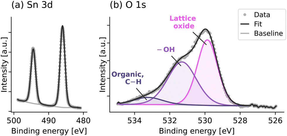 | ||
| Fig. 5 XPS spectra of Sn 3d and O 1s core levels of the SnO deposited with 1 x Sn pulse mode. XPS was performed ex situ, without any etching of the SnO surface. | ||
The optical properties of the p-type SnO films have been analysed using the absorption coefficient to produce Tauc plots (provided in the ESI,† Fig. S2 and S3) and allowing the extraction of the direct, optical band gap. The SnO films deposited with a single Sn pulse showed a direct band gap of 2.93 eV after vacuum annealing, reducing to 2.86 eV and 2.83 eV with the introduction of multiple Sn pulses and multiple pulses with exposure mode respectively. This is consistent with the values of direct band gap reported elsewhere for SnO, in the range of 2.7–3.4 eV.1,2,6
3.2 Device performance
Fig. 6 demonstrates the effect of the post deposition annealing, (a), (b), and passivation (c), (d) on the performance of SnO TFTs deposited using exposure mode. | ||
| Fig. 6 P-type SnO TFT performance at Vd = −1 V and devices passivated with ∼20 nm ALD alumina showing: the effect of post deposition annealing on (a) the gate transfer characteristics and (b) the field effect mobility curves; and the effect of Al2O3 passivation on (c) the gate transfer characteristics, with threshold voltage inset, and (d) the field effect mobility curve. | ||
It can be seen from the gate transfer curve in Fig. 6(a) that the as-deposited SnO film was very resistive, with a higher gate leakage current (|Ig|, dotted line) than drain current (|Id|), and demonstrated no switching as the gate was swept from 50 to −50 V. This is improved significantly after post deposition annealing with the on-state current (negative voltages) increasing to ∼1 × 10⁻⁵ A and further to ∼4 × 10⁻⁴ A as the annealing temperature increased from 250 °C to 350 °C. In addition, the threshold voltage shifts towards zero from 12.8 V to 9.3 V. Looking at Fig. 6(b) we see a similar picture, with a significant improvement in the field effect mobility (μFE) as the annealing temperature is increased. Annealing at 250 °C and 350 °C achieves a maximum μFE of 0.68 cm2 (V s)−1 and 2.3 cm2 (V s)−1 respectively.
However, as all this happens, the off-state current also increases (Fig. 6(a)), meaning that the on–off ratio actually decreases from 3.7 × 10⁴ to 3.2 × 10³, and the subthreshold swing increases from 5.95 V dec−1 to 11.5 V dec−1, showing that raising the annealing temperature to 350 °C sacrifices the TFT performance for only a marginal gain in on-state current and threshold voltage. This trend was seen across both the films deposited in the 3 x Sn pulse mode and 3 x Sn pulse with exposure mode (see Table 2).
| V th (V) | μ FE (cm2 (V s)−1) | SS (V dec−1) | I on/Ioff | I max (A) | ||
|---|---|---|---|---|---|---|
| 1 x Sn pulse | ||||||
| Annealed: | 250 °C | — | — | — | — | — |
| 350 °C | −0.6 | 0.17 | 8.8 | 4.5 × 10³ | 1.9 × 10⁻⁶ | |
| 3 x Sn pulse | ||||||
| Annealed: | 250 °C | 11.6 | 0.60 | 6.2 | 4.0 × 10⁴ | 9.7 × 10⁻⁶ |
| 350 °C | 6.5 | 2.22 | 11.7 | 3.1 × 10³ | 3.9 × 10⁻⁵ | |
| 3 x Sn pulse + exposure | ||||||
| Annealed: | 250 °C | 12.8 | 0.68 | 6.0 | 3.7 × 10⁴ | 1.1 × 10⁻⁵ |
| 350 °C | 9.3 | 2.27 | 11.5 | 3.2 × 10³ | 4.2 × 10⁻⁵ | |
This is consistent with other findings for the post deposition annealing of p-type metal oxides,14,34 where the higher annealing temperature increases the size of the film crystallites and reduces the number of grain boundaries, in turn increasing the mobility and on-state current. The subsequent increase in the off-state current has also been reported in other work, where it has been attributed both to disproportionation to metallic Sn14 and n-type SnO2,12 both of which would provide a source of electrons and inhibit the device switching off. This phenomenon highlights one of the consistent difficulties of p-type SnO: the inherent instability of the oxidation state. However, the results here and reported elsewhere12,14 suggest that it may be possible to manage this with careful annealing optimisation.
Fig. 6(c) shows that passivation with ALD Al2O3 increases the on–off ratio, shifts the threshold voltage towards zero and improves the hysteresis, and Fig. 6(d) increases the field effect mobility of the SnO devices. Passivation, or device capping, is used to protect devices from environmental exposure that may affect their performance or stability,35 but also to reduce the back-channel trap states, which has been shown for both SnO11,16 and Cu2O.36 This effect has been presented for films annealed at 350 °C, but similar behaviour was seen for films annealed at 250 °C. Given the improved device performance after Al2O3 passivation, this was used as standard for all the SnO devices discussed from this point.
Fig. 7 shows a comparison of (a) the gate transfer characteristics (Id) and gate leakage current (Ig, measured as the current through the gate contact) and (b) μFE for each precursor delivery mode, annealed at 350 °C and passivated with ALD Al2O3.
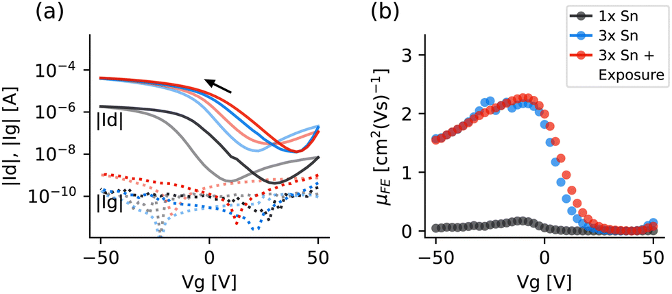 | ||
| Fig. 7 Comparison of TFT performance with precursor delivery mode, showing (a) gate transfer characteristics and (b) field effect mobility. | ||
It is immediately clear that the devices deposited with multiple Sn pulses achieve an order of magnitude improvement in the on-state current, from ∼2 × 10⁻⁶ A to ∼4 × 10⁻⁵ A, but that the on/off ratios are very similar for all modes, at 4.5 × 10³, 3.1 × 10³ and 3.2 × 10³ for the 1 x Sn mode, 3 x Sn mode and 3 x Sn with exposure mode respectively. In addition, there is also greater hysteresis for the 1 x Sn mode, which can be seen very clearly in the output curves included in the ESI,† Fig. S5–S7. Table 2 provides a summary of the TFT performance for each mode of precursor delivery and purge, annealed at 250 °C and 350 °C.
The clear difference in performance between the 1 x Sn pulse mode and the 3 x Sn pulse modes, can likely be linked back to the XRD patterns (Fig. 4) and the lack of crystallinity seen for the 1 x Sn mode. This could also explain why the devices deposited using the 1 x Sn mode remained unmeasurable when annealed at 250 °C as a more disordered starting state would likely require a higher annealing temperature or a longer anneal. However, XRD of the annealed films would be required to explore this fully. This is also consistent with the Hall effect measurement data for the 1 x Sn pulse mode provided in the ESI† (Table S1). Whereas, the similarity in performance for the two devices using 3 Sn pulses (with and without exposure mode), suggests that despite the difference in crystallinity seen in the XRD patterns, the post deposition annealing brings the films to a very similar state.
Fig. 8 provides the capacitance–voltage (C–V) characteristics comparing both the temperature of post deposition vacuum annealing (a) and precursor delivery mode (b).
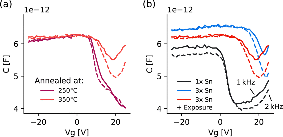 | ||
| Fig. 8 C–V characteristics at a frequency of 1 kHz (solid line) and 2 kHz (dashed line), showing (a) a comparison of post deposition vacuum annealing temperature for films deposited using 3 x Sn with exposure mode and (b) a comparison of precursor delivery mode for films annealed at 350 °C. | ||
Comparing the devices annealed at different temperatures, it is clear that they behave very similarly in the on-state (negative Vg) but differently in the off-state (positive Vg). For the film annealed at 350 °C, there is clear ambipolar behaviour with an increase of capacitance in the off-state, whereas over the voltage range shown, there is no equivalent increase for the film annealed at 250 °C. The fact that the capacitance decreases and then increases again as the voltage becomes more positive for the 350 °C curve, shows that there is a build up of minority carriers, creating negative charge, rather than that the majority carriers (holes) not being depleted effectively. This behaviour is consistent with the difference seen in the gate transfer characteristics of Fig. 6(a) and Table 2, where there is an order of magnitude decrease in the on–off ratio due to the increased off-state current for the film annealed at 350 °C. As discussed already, this phenomenon has been reported elsewhere, with the electron conduction attributed to both Sn and SnO2 formation at higher annealing temperatures.12,14
For the three different modes of precursor delivery and purge, shown in Fig. 8(b), there is an increase of charge in the on-state for all three. However, interestingly the C–V for the 1 x Sn mode shows a clearer transition from depletion to accumulation, occurring at ∼0 V. This correlates with the value of Vth (−0.6 V) given in Table 2. In contrast, for the 3 x Sn modes, the transition from depletion to accumulation occurs much earlier, at positive Vg, which again correlates with the larger, positive values of Vth given in Table 2 for the 3 x Sn modes. This again indicates the accumulation of minority carriers in the off-state, rather than hole depletion.
3.3 AFM growth analysis for the different modes of precursor delivery
Fig. 9 shows atomic force microscope (AFM) images of the surface of films deposited in each of the three modes, prior to any post deposition annealing, where the height variation, H(x,y), is taken as the variation from the mean surface height:| H(r) ≡ z(r) − 〈z(r)〉 | (1) |
 | ||
| Fig. 9 AFM images of the as-deposited film surface for the three different precursor delivery modes. | ||
As can be seen from Figure (a), the film surface for the 1 x Sn pulse mode is much smoother than the other two precursor delivery modes (very little variation in H(x,y)), with no clear crystals or grains visible. This is consistent with the XRD data (Fig. 4) that suggested the 1 Sn pulse deposited film was amorphous with no detectable XRD peaks.
This variation in roughness can be quantified by the vertical roughness, given by the root mean square of H(r),37 or the RMS roughness (δ), and the lateral roughness, which is usually quantified by the correlation length (σ). Both of these can be calculated from the autocovariance function,37 which provides a quantitative measure of how the heights at different r are correlated with each other as a function of their separation |r|.
Assuming a Gaussian form, the correlation length (σ) and RMS roughness (δ) are determined by the width and height respectively:
 | (2) |
Fig. 10 shows the autocovariance functions for the AFM images shown in Fig. 9, computed by taking the 2D Fast Fourier Transform (FFT) of the AFM images to give the power spectral density (PSD) and then the 2D Inverse Fast Fourier Transform (IFFT) of the PSD. These 2D functions have then been averaged and binned radially over r to give a 1-dimensional profile, except for the 1 x Sn pulse mode, for which the height variation along the surface was of the same order as the line artefacts introduced by concatenating the data along the slow-scan direction to produce the AFM image and therefore only the 1D FFT was used along the fast-scan axis, then averaged and binned along the slow-scan axis. The black line shows a Gaussian fit with the extracted values for δ and σ given for each mode of precursor delivery.
 | ||
| Fig. 10 Radially averaged autocovariance function of the AFM images for the three modes of precursor delivery, showing a Gaussian fit in black, and the fit residual plotted above, which allowed the extraction of σ and δ as given in eqn (2). | ||
When looking at Fig. 10, the first thing to note is that Figure (b) and (c) are quite similar, which is perhaps to be expected given the similar TFT performances of the 3 x Sn with and without exposure modes. However, this similarity highlights the huge difference in the δ value extracted for the 1 Sn pulse mode (0.02 nm), for a σ value that is very similar to the other precursor delivery modes. This demonstrates a significant difference in the surface structure between the 1 Sn pulse mode and 3 Sn pulse modes. The XRD data provided crystallite dimensions of 16.38 nm and 14.78 nm in the C-axis for films obtained from the 3 x Sn and 3 x Sn with exposure mode processes respectively. The detection of only the [001] and [002] c-axis reflections is consistent with crystallites growing with the a-and b-axes lying parallel with the substrate. The dimensions in these axes is then observed via AFM, with values extracted for σ corresponding to the crystallite size in the plane of the substrate. This suggests that the particles can be considered as wide flat plates with a thickness in the c-axis given by the XRD data and dimensions in the a- and b-axes equal to σ Although δ and σ provide a quantitative comparison of the film surface, they provide only a snapshot of the surface state at a specific time/thickness and don’t, by themselves, provide any insight to differences in the growth mechanism. However, these quantities scale with time (assuming steady delivery of precursor to the growing surface), allowing the use of topographical scaling methods and fractal geometry.37 However, in this ALD process, as the growth is not steady with time, the analysis should be considered as scaling with thickness instead.
Assuming the surface of growing films to be statistically self-affine and studying how both δ and σ scale with time, Family and Viscek showed that δ and σ can be related by:37–39
 | (3) |
The scaling nature of growing self-affine films is determined by the balance between competing roughening and smoothing mechanisms.37 Deposition of thin films has an inherent randomness associated with the stochastic nature of the deposition flux on the surface; if there were no additional smoothing or roughening mechanisms, the surface will grow under the mechanism of stochastic roughening and will have a β value of 1/2 and α of 0, as growth is completely random and therefore there is no correlation along the surface.40 ALD is a process driven by surface absorption, rather than bombardment (as expected for sputtered films), and will therefore have inherent smoothing mechanisms at play, demonstrated by the high conformality and uniformity of ALD films.41,42
Depending on which smoothing mechanisms are introduced, the values of α and β will change, therefore α and β provide a fingerprint of the dominant smoothing mechanisms at play during film growth.
Based on work by Herring,43 who analysed the scaling processes of sintering, Mullins showed that the dominant smoothing mechanism could be most easily extracted in Fourier space using:
 | (4) |
and the exponent i takes an integer value determined by the dominant smoothing mechanism.44

The four smoothing mechanisms considered were: viscous flow (i = 1) or creep of an amorphous material which is driven by higher surface tension under a convex surface than under a concave surface, thus driving material from convex to concave regions; evaporation and condensation (i = 2) driven by the higher vapour pressure over a convex surface than a concave surface; volume diffusion (i = 3) or bulk diffusion of material driven by a local gradient in the chemical potential; surface diffusion (i = 4) or surface migration of material driven by a gradient in the chemical potential within the surface plane.43,45 For the case where stochastic roughening dominates the surface morphology, i = 0.
By combining eqn (4) with a noise term to represent the stochastic roughening mechanism and solving analytically gives:37
 | (5) |
Therefore for large q, it can be seen that the PSD approaches
 | (6) |
From this and using an approximation for g(|q|) in terms of α, Tong and Williams37 showed that i could be related to α with the following:
| i = 2(α + 1) | (7) |
Fig. 11 shows the PSD for the three modes of precursor delivery, calculated using the 2D FFT and averaged and binned radially (or 1D FFT and averaged along the slow-scan axis for the 1 Sn mode). The size of the image used has been chosen to ensure that the x- and y-dimensions are larger than the lateral correlation length calculated in Fig. 10, but that the majority of the data is at a large enough q to approach the straight line fit given in eqn (6). Rather than fit a straight line using a linear regression, lines representing each of the different smoothing mechanisms (i = 0, 1, 2, 3, 4) have been plotted in as a guide (dashed lines), with the best fit highlighted in black.
 | ||
| Fig. 11 Radially averaged power spectrum density of the AFM images for the three modes of precursor delivery, with straight line fits for the 4 theoretical smoothing mechanism provided as a guide (dashed grey lines) and the best fit highlighted in black. | ||
Looking at the best fit for i, suggests that the dominant smoothing mechanism for the 1 Sn pulse mode (a), was viscous flow (i = 1), whereas the dominant mechanism for the 3 Sn pulse modes, (b) & (c), was volume diffusion (i = 3). Using eqn (7) gives α = −0.5 and 0.5 for i = 1 and 3 respectively.
Firstly looking at the 1 Sn pulse mode where i = 1 and α = −0.5, it is necessary to think what a negative value of α means physically. Using eqn (3) and rearranging gives:
| δ = σα | (8) |
Therefore with negative α, the RMS roughness (δ) will decrease as the lateral correlation length (σ) increases with thickness. This could be described by 2D island deposition where the films grow laterally along the surface,45 increasing the lateral correlation length whilst simultaneously reducing the roughness, which would be consistent with the hypothesis that the for the 1 Sn pulse mode, the Sn precursor dose was insufficient to result in full (or saturated) surface adsorption and complete monolayer deposition per cycle.
Alternatively, as eqn (8) does not describe the relationship with thickness, it could be interpreted conversely: decreasing σ as δ increases with thickness. However, given the very small δ and relatively large σ extracted from Fig. 10, it suggests that the growth evolution would show increasing σ and decreasing δ.
In comparison, the 3 Sn pulse modes without (b) and with (c) exposure mode have a positive value of α (0.5) showing that δ and σ will scale with each other (either both smaller with increasing thickness or both larger with increasing thickness), but that as α = 0.5, σ will scale faster than δ; the surface undulations will spread laterally more than they grow vertically. Fig. 11 determines that this spreading or smoothing mechanism is dominated by volume diffusion, within the bulk deposited film. This is perhaps unexpected for an ALD process, where we expect the reaction to be self terminating, resulting in growth of a full monolayer per cycle. This could suggest that the deposition is not within the pure ALD regime. The higher precursor dose could mean that a longer purge cycle is required to ensure there is no direct reaction between the alternating precursors. Whether this is the case would have to be confirmed by further work looking at the effect on growth rate as the purge length is varied.
4 Conclusions
This work has demonstrated the successful atomic layer deposition of SnO films using Sn(II) bis-(tert-butoxide), confirmed through XRD patterns, and the fabrication of working p-type SnO TFTs. The ALD process has been investigated in terms of the Sn precursor pulse length and the substrate temperature, and three different modes of precursor delivery have been explored: 1 Sn pulse per cycle, 3 Sn pulses per cycle and 3 Sn pulses per cycle with exposure (where the pump is stopped for a short while after the last Sn precursor pulse to increase the residence time of the precursor).The introduction of multiple Sn pulses significantly improved the conductivity and mobility of the devices with the on-state current (Imax) increasing from 1.9 × 10⁻⁶ A to 3.9 × 10⁻⁵ A and μFE from 0.17 cm2 (V s)−1 to 2.22 cm2 (V s)−1 when the precursor delivery mode was switched from 1 x Sn pulse to 3 x Sn mode. Although there was a further increase in both to 4.2 × 10⁻⁵ A and 2.27 cm2 (V s)−1 when the exposure mode was introduced, the improvements were marginal under these conditions and therefore, by themselves, do not justify the greater cycle length and subsequent lower growth rates associated with the exposure mode. However, one other consideration is the more conformal deposition, identified by the smaller error bars in Fig. 3(d), which would be significant for commercial applications and would perhaps justify the longer cycle length if this was phenomenon was also seen in other ALD systems. All the devices required post deposition annealing and as the annealing temperature increased from 250 °C to 350 °C for devices deposited with 3 Sn pulses with exposure mode, μFE increased from 0.68 cm2 (V s)−1 to 2.3 cm2 (V s)−1, but at the same time, the on–off ratio decreased from ∼104 to ∼103. This was attributed to the incorporation of defects that act as a source of electrons in the off-state, demonstrated by an increase in capacitance in the off-state, showing the build up of minority carriers.
Finally, the use of fractal geometry and topographical scaling methods confirmed a significant difference in the dominant deposition mechanisms present for the 1 x Sn pulse mode relative to the 3 x Sn pulse modes, with analysis of the 1 x Sn mode suggesting deposition involved 2D island growth rather than full monolayer growth per cycle.
Overall, this work has demonstrated successful p-type TFTs with the best device, deposited with 3 x Sn pulses per cycle and annealed at 250 °C post deposition, achieving a μFE of 0.6 cm2 (V s)−1, SS of 0.6 V dec−1 and on–off ratio of 4 × 10⁴. Although the on–off ratio has been limited here due to a high off-state current, this current could be suppressed by careful optimisation of the thickness of the SnO active layers as demonstrated by Kim et al.16 to increase the on–off ratio to the desirable value of 106.
Author contributions
D. Gomersall prepared the original draft; KM Niang, JD Parish, AJ Flewitt and AL Johnson reviewed and edited the article; D. Gomersall and KM Niang carried out the experiments; JD Parish performed the precursor synthesis; and Z. Sun collected the XPS data. All authors approved the final manuscript.Conflicts of interest
There are no conflicts to declare.Acknowledgements
This work is supported by the EPSRC through the Centre for Doctoral Training in Integrated Photonic and Electronic Systems (IPES) under grant no. EP/L015455/1, and through project grants EP/M013650/1 and EP/P027032/1. For the purpose of open access, the author has applied a Creative Commons Attribution (CC BY) licence to any Author Accepted Manuscript version arising from this submission.Notes and references
- Z. Wang, P. K. Nayak, J. A. Caraveo-frescas and H. N. Alshareef, Adv. Mater., 2016, 28, 3831–3892 CrossRef CAS PubMed
.
- E. Fortunato, P. Barquinha and R. Martins, Adv. Mater., 2012, 24, 2945–2986 CrossRef CAS PubMed
- Y. Li, J. Yang, Y. Wang, P. Ma, Y. Yuan, J. Zhang, Z. Lin, L. Zhou, Q. Xin and A. Song, IEEE Electron Device Lett., 2018, 39, 208–211 CAS
- J. Yang, Y. Wang, Y. Li, Y. Yuan, Z. Hu, P. Ma, L. Zhou, Q. Wang, A. Song and Q. Xin, IEEE Electron Device Lett., 2018, 39, 516–519 CAS
- N. C. A. van Fraassen, K. M. Niang, J. D. Parish, A. L. Johnson and A. J. Flewitt, Sci. Rep., 2022, 12, 1–12 CrossRef PubMed
- H. M. Kim, S. H. Choi, H. J. Jeong, J. H. Lee, J. Kim and J. S. Park, ACS Appl. Mater. Interfaces, 2021, 13, 30818–30825 CrossRef CAS PubMed
- A. Togo, F. Oba, I. Tanaka and K. Tatsumi, Phys. Rev. B: Condens. Matter Mater. Phys., 2006, 74, 195128 CrossRef
- I. T. Cho, U. Myeonghun, S. H. Song, J. H. Lee and H. I. Kwon, Semicond. Sci. Technol., 2014, 29, 045001 CrossRef CAS
- J. A. Caraveo-Frescas, P. K. Nayak, H. A. Al-Jawhari, D. B. Granato, U. Schwingenschlögl and H. N. Alshareef, ACS Nano, 2013, 7, 5160–5167 CrossRef CAS PubMed
- E. Fortunato, R. Barros, P. Barquinha, V. Figueiredo, S. H. K. Park, C. S. Hwang and R. Martins, Appl. Phys. Lett., 2010, 97, 052105 CrossRef
- K.-H. Bae, M. G. Shin, S.-H. Hwang, H.-S. Jeong, D.-H. Kim and H.-I. Kwon, IEEE Access, 2020, 8, 222410 Search PubMed
- H. Yabuta, N. Kaji, R. Hayashi, H. Kumomi, K. Nomura, T. Kamiya, M. Hirano and H. Hosono, Appl. Phys. Lett., 2010, 97, 072111 CrossRef
- H.-N. Lee, H.-J. Kim and C.-K. Kim, Jpn. J. Appl. Phys., 2010, 49, 020202 CrossRef
- K. Okamura, B. Nasr, R. A. Brand and H. Hahn, J. Mater. Chem., 2012, 22, 4607 RSC
- Y. Ogo, H. Hiramatsu, K. Nomura, H. Yanagi, T. Kamiya, M. Hirano and H. Hosono, Appl. Phys. Lett., 2008, 93, 032113 CrossRef
- S. H. Kim, I.-H. Baek, D. H. Kim, J. J. Pyeon, T.-M. Chung, S.-H. Baek, J.-S. Kim, J. H. Han and S. K. Kim, J. Mater. Chem. C, 2017, 5, 3139 RSC
- A. L. Johnson and J. D. Parish, ACS Symp. Ser., 2018, 1311, 1–53 CrossRef
- N. Huster, R. Ghiyasi, D. Zanders, D. Rogalla, M. Karppinen and A. Devi, Dalton Trans., 2022, 51, 14970–14979 RSC
- M. S. Hill, A. L. Johnson, J. P. Lowe, K. C. Molloy, J. D. Parish, T. Wildsmith and A. L. Kingsley, Dalton Trans., 2016, 45, 18252–18258 RSC
- A. Mameli, J. D. Parish, T. Dogan, G. Gelinck, M. W. Snook, A. J. Straiton, A. L. Johnson and A. J. Kronemeijer, Adv. Mater. Interfaces, 2022, 9, 2101278 CrossRef CAS
- D. Pan, L. Ma, Y. Xie, T. C. Jen and C. Yuan, J. Vac. Sci. Technol., A, 2015, 33, 021511 CrossRef
- J. H. Han, Y. J. Chung, B. K. Park, S. K. Kim, H. S. Kim, C. G. Kim and T. M. Chung, Chem. Mater., 2014, 26, 6088–6091 CrossRef CAS
- R. L. Puurunen, J. Appl. Phys., 2005, 97, 121301 CrossRef
- J. Tupala, M. Kemell, M. Mattinen, K. Meinander, S. Seppälä, T. Hatanpää, J. Räisänen, M. Ritala and M. Leskelä, J. Vac. Sci. Technol., A, 2017, 041506 CrossRef
- J. H. Lee, M. Yoo, D. Kang, H. M. Lee, W. H. Choi, J. W. Park, Y. Yi, H. Y. Kim and J. S. Park, ACS Appl. Mater. Interfaces, 2018, 10, 33335–33342 CrossRef CAS PubMed
- H. Beh, D. Hiller and M. Zacharias, Phys. Status Solidi A, 2018, 215, 1700880 CrossRef
- L. Nyns, A. Delabie, M. Caymax, M. M. Heyns, S. Van Elshocht, C. Vinckier and S. De Gendt, J. Electrochem. Soc., 2008, 155, G269 CrossRef CAS
-
H. C. Knoops, S. E. Potts, A. A. Bol and W. M. Kessels, Handb. Cryst. Growth Thin Film. Ep., North-Holland, 2nd edn, 2015, pp.1101–1134 Search PubMed
- K. M. Niang, G. Bai and J. Robertson, J. Vac. Sci. Technol., A, 2020, 38, 042401 CrossRef CAS
- E. R. Cleveland, L. Henn-Lecordier and G. W. Rubloff, J. Vac. Sci. Technol., A, 2012, 30, 01A150 CrossRef
- A. I. Aria, K. Nakanishi, L. Xiao, P. Braeuninger-Weimer, A. A. Sagade, J. A. Alexander-Webber and S. Hofmann, ACS Appl. Mater. Interfaces, 2016, 8, 30564 CrossRef CAS PubMed
- T. Daeneke, P. Atkin, R. Orrell-Trigg, A. Zavabeti, T. Ahmed, S. Walia, M. Liu, Y. Tachibana, M. Javaid, A. D. Greentree, S. P. Russo, R. B. Kaner and K. Kalantar-Zadeh, ACS Nano, 2017, 11, 10974–10983 CrossRef CAS PubMed
- D. Barreca, A. Milanov, R. A. Fischer, A. Devi and E. Tondello, Surf. Sci. Spectra, 2021, 14, 34 CrossRef
- S. Han, K. M. Niang, G. Rughoobur and A. J. Flewitt, Appl. Phys. Lett., 2016, 109, 3502 Search PubMed
- J. K. Jeong, H. W. Yang, J. H. Jeong, Y. G. Mo and H. D. Kim, Appl. Phys. Lett., 2008, 93, 123508 CrossRef
- M. Napari, T. N. Huq, D. J. Meeth, M. J. Heikkilä, K. M. Niang, H. Wang, T. Iivonen, H. Wang, M. Leskelä, M. Ritala, A. J. Flewitt, R. L. Z. Hoye and J. L. MacManus-Driscoll, ACS Appl. Mater. Interfaces, 2021, 13, 4156–4164 CrossRef CAS PubMed
- W. M. Tong and S. R. Williams, Annu. Rev. Phys. Chem., 1994, 45, 401–439 CrossRef CAS
- F. Family and T. Vicsek, J. Phys. A: Math. Gen., 1985, 18, 75–81 CrossRef
- F. Family, Phys. A, 1990, 168, 561–580 CrossRef
-
A.-L. Barabási and H. E. Stanley, Fractal Concepts in Surface Growth, Cambridge University Press, 1995 Search PubMed
-
L. A. Chow, Handbook of Thin Film Depostion: Techniques, Processes and Technologies, Elsevier Inc., 3rd edn, 2012, ch. 6, pp.127–178 Search PubMed
- P. French, G. Krijnen and F. Roozeboom, Microsyst. Nanoeng., 2016, 2, 16048 CrossRef CAS PubMed
- C. Herring, J. Appl. Phys., 1950, 21, 301–303 CrossRef CAS
- W. W. Mullins, J. Appl. Phys., 1959, 30, 77 CrossRef
- A. J. Flewitt, J. Robertson and W. I. Milne, J. Appl. Phys., 1999, 85, 8032 CrossRef CAS
Footnote |
| † Electronic supplementary information (ESI) available: Hall measurements, Tauc plots, XPS data and TFT output curves. See DOI: https://doi.org/10.1039/d3tc00255a |
| This journal is © The Royal Society of Chemistry 2023 |