
 Open Access Article
 This Open Access Article is licensed under a
 Creative Commons Attribution 3.0 Unported Licence
Organic copolymer lasing from single defect microcavity fabricated using laser patterning†
Peter
Claronino
 ab,
Rahul
Jayaprakash
a,
Till
Jessewitsch
c,
Rachel C.
Kilbride
d,
Timothy
Thornber
a,
Alina
Muravitskaya
b,
Robert D. J.
Oliver
a,
Ullrich
Scherf
e,
Jean-Sebastien G.
Bouillard
b,
Ali M.
Adawi
*b and
David G.
Lidzey
*a
ab,
Rahul
Jayaprakash
a,
Till
Jessewitsch
c,
Rachel C.
Kilbride
d,
Timothy
Thornber
a,
Alina
Muravitskaya
b,
Robert D. J.
Oliver
a,
Ullrich
Scherf
e,
Jean-Sebastien G.
Bouillard
b,
Ali M.
Adawi
*b and
David G.
Lidzey
*a
aDepartment of Physics and Astronomy, The University of Sheffield, Hicks Building, Hounsfield Road, Sheffield S3 7RH, UK. E-mail: d.g.lidzey@sheffield.ac.uk
bDepartment of Physics and Mathematics, University of Hull, Robert Blackburn Building, Hull HU6 7RX, UK. E-mail: a.adawi@hull.ac.uk
cOrganic Functional Molecules, Organic Chemistry, University of Wuppertal, Gaußstrasse 20, 42119 Wuppertal, Germany
dDepartment of Chemistry, The University of Sheffield, Dainton Building, Brook Hill, Sheffield, S3 7HF, UK
eMacromolecular Chemistry Group and Wuppertal Center for Smart Materials & Systems (CM@S), Bergische Universität Wuppertal, Gauss-Strasse 20, 42119 Wuppertal, Germany
First published on 24th March 2023
Abstract
Reducing the lasing threshold in optically pumped organic lasers is a necessary component of the drive to develop an organic laser diode, as this may help mitigate the losses associated with electrical contacts and charge injection. In this study we show how increasing the binaphthyl (BN) spacer content in polydioctylfluorene (PFO) decreases its amplified spontaneous emission threshold (ASE) through the suppression of intermolecular interactions. Using co-polymers with low lasing thresholds, we use a laser patterning technique to fabricate physical defects (having a diameter of ∼2.5 μm) within a vertical microcavity. Such defects create additional lateral confinement, with this approach allowing us to reduce the lasing threshold from 11 μJ cm−2 to 7 μJ cm−2 and increase cavity Q-factor from 495 (planar cavity) to 2300. The enhanced performance and the stack structure of the defect microcavity show it is a promising architecture for an electrically-pumped laser device.
10th Anniversary StatementOver the past 9 years, the Electronic and Photonic Molecular Materials Group at the University of Sheffield have published on average one paper per year in the Journal of Materials Chemistry C (JMCC). This work has covered a wide and diverse range of topics, ranging from nanoscale chemical sensors, polariton condensation in organic-semiconductor microcavities, the exploration of molecular aggregate states in BODIPY-dyes and the optimisation of both polymer and perovskite solar cells. It is the wide breadth of topics covered by JMCC that make it an attractive journal for researchers working at the interface of physics, chemistry and materials science, with topics covered ranging from photonics to photovoltaics via lasers and displays. We believe JMCC to be a high quality journal with a promising Impact Factor and a fast turn-around. Indeed, our JMCC papers have achieved good visibility, with some being very well cited. We wish JMCC continued success over the next 10 years and look forward to publishing further papers in this journal. |
Introduction
Organic semiconductor lasers (OSL) are a popular area of research due to their low lasing threshold, film flexibility, and wavelength tunability,1–3 with recent reports demonstrating lasing at wavelengths approaching 900 nm.4–6 These attributes allow organic lasers to find possible applications in sensing,7 displays, photonic barcodes,8 lab-on-chip devices,9 and short range on-chip or chip-to-chip data communications.10 Organic semiconductors can act as an efficient gain medium as they have high quantum yields and low reabsorption losses due to large Frank–Condon shifts, which result in low lasing thresholds. Extremely low thresholds have been reported in optically pumped OSLs,1 and organic laser diodes recently demonstrated,11 however it is clear that generating lasing through electrical excitation still remains challenging.12 The most detrimental losses occur due to charge absorption from polarons,10 and the additional triplet states that are formed along with singlets in a ratio of singlets![[thin space (1/6-em)]](https://www.rsc.org/images/entities/char_2009.gif) :triplets of 1:3. This has been supported by optical simulations that suggest the depopulation of singlets through singlet–triplet annihilation is the dominant loss mechanism preventing lasing.13 As the losses from electrical pumping are so high, the predicted thresholds for electrically pumped lasers are greater than 500 A cm−2.13
:triplets of 1:3. This has been supported by optical simulations that suggest the depopulation of singlets through singlet–triplet annihilation is the dominant loss mechanism preventing lasing.13 As the losses from electrical pumping are so high, the predicted thresholds for electrically pumped lasers are greater than 500 A cm−2.13
To lower lasing thresholds a multitude of different materials and resonator structures has been explored, with such structures generally being excited by optical pumping. Following such an approach, materials with improved triplet management can demonstrate lasing under quasi-continuous wave (CW) conditions and have been shown to be promising candidates for electrical excitation.14–17 The polymer polyfluorene 2,7-(9,9-dioctylfluorene) (PFO) has been explored for lasing applications, with modifications to its structure being explored as a means to improve both its lasing characteristics and its charge-carrier mobility.18 One of the most promising copolymer variants of PFO involves including binaphthyl (BN) spacer groups between the monomer units, where it is reported that increasing the degree of BN copolymerisation decreases the lasing threshold.19 It has been proposed that the inclusion of these spacer groups affects the molecular packing of the polymer chains and can suppress the formation of the β-phase in spin cast films. Such reductions in the formation of the β-phase have been reported to improve its lasing performance.19
An alternate approach to reduce lasing thresholds is to create optical feedback structures that confine light at the wavelength scale in an organic semiconductor and thereby increase optical gain. This has been achieved in photonic crystals,20,21 distributed-feedback gratings (DFB),22 random lasing from multilayer cracks21,23 and microcavities24 using coherent optical scattering effects. Here, DFBs provide feedback by scattering waveguided light using a periodic grating that allows light having a single wavelength to propagate through the gain medium. Other significant optical gain structures include whispering gallery mode resonators22–26 in which light is waveguided in spherical closed loop structures, with the path length of one trip being a multiple of half a wavelength. The complex structure of gratings and whispering gallery mode resonators make integration into light emitting diode (LED) devices challenging and the long optical path length results in a lower spontaneous emission factor.27
Optical microcavities are also a promising type of optical resonator used to reduce lasing thresholds. Significantly, they can be readily integrated into conventional organic light emitting diodes (OLEDs), allowing charge to be injected into the semiconductor gain medium.28 Optical microcavities are comprised of two highly reflective mirrors placed either side of a gain medium. Such mirrors can be made from reflective metals, however Distributed Bragg Reflectors (DBR) are often used as they can be engineered to have a reflectivity above 99%, allowing very low lasing thresholds to be demonstrated.29 Fine control over cavity mode wavelength can also be achieved through control of the organic gain layer thickness. By ensuring that the microcavity optical path length is on the order of half the lasing wavelength, it is possible to generate single mode confinement which encourages the emission of spontaneously emitted photons into a single lasing mode which reduces the lasing threshold.30 The first polymer microcavity laser was reported in 1996 using poly(p–phenylenevinylene) (PPV) as the gain medium, with a DBR bottom mirror and silver top mirror.24 Follow-on studies now generally use DBRs as both top and bottom mirror to improve the lasing performance.31
Further reductions in lasing threshold can be achieved by decreasing the mode volume within a microcavity; an effect achieved through the use of focused ion beam (FIB) milling to create micropillars,32 or by patterning deformations that add lateral confinement.33–37 An evaporation technique using a shadow mask with a set of rectangular openings has also been used to define such features.38 We have recently developed a simple optical patterning method to engineer lateral confinement in a microcavity, which allows large arrays of defects to be rapidly fabricated.39 Such lateral confinement generates additional transverse modes that can be spectrally resolved using k-space (Fourier) imaging.
Here, we report a study on a random polyfluorene-type copolymer (BN-PFO, Fig. 1(a)), specifically a poly[2,7-(9,9-dioctylfluorene)] with different fractions (5.2, 9.8, or 12.7 mol%) of 6,6′-(2,2′-dioctyloxy-1,1′-binaphthyl) repeat units. Significantly, this polymer has been shown to undergo quasi-CW lasing with low lasing thresholds.40 Lasing from BN-PFO has been previously reported in DFBs, containing first and second order gratings,41 together with non-periodic circular gratings.42 In the work described here, we firstly investigate how the lasing performance of BN-PFO is affected by the relative concentration of the BN units and intermolecular packing. After having established which materials have the lowest gain thresholds, we then fabricate planar microcavity structures and use our recently developed laser patterning technique to write physical ‘defect’ structures inside the microcavity. We characterise emission from such structures using a Fourier imaging technique that reveals a modified optical mode structure. We show that such defect structures generate lateral optical-confinement, increase cavity Q-factor and reduce lasing thresholds from 11 μJ cm−2 to 7 μJ cm−2. This threshold is consistent with other reports using the same copolymer placed in a DFB,40–42 (the lowest reported threshold being 1.2 μJ cm−2) and is lower than thresholds reported for other polymer DBR microcavities with similar structures (84 μJ cm−2).31
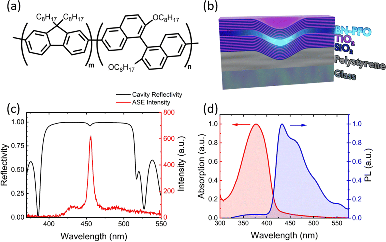 | ||
| Fig. 1 (a) Molecular structure of BN-PFO consisting of PFO (m) with repeat units of BN (n). (b) Microcavity structure: quartz/PS (with defect)/10.5 Pair DBR/BN-PFO (12.7 mol% binaphthyl)/7.5 pair DBR. Note that the relative depth of the defect structure is increased significantly for the sake of clarity. (c) Total simulated cavity reflectivity (left) centred at the peak of ASE spectra (right). (d) BN-PFO absorption (left) and photoluminescence (right). | ||
Experimental
Materials and sample preparation
All substrates were first sequentially cleaned in Hellmanex, deionised water and isopropanol. Substrates were then dried with a nitrogen gun and exposed to UV Ozone for 15 minutes. In all experiments described, the conjugated polymer BN-PFO with different fractions of BN have been explored as the gain medium. BN-PFO was synthesized by Yamamoto-type coupling with racemic binaphthyl monomer with the corresponding molecular weights: 5.2% (Mn = 94.8 kDa, Mw = 178 kDa), 9.8% (Mn = 68.3 kDa, Mw = 131 kDa), and 12.7% (Mn = 80.7 kDa, Mw = 158 kDa). Here, BN content was calculated by H-NMR and molecular weight were determined by gel permeation chromatography (0.5 mg mL−1 in chloroform). This range of BN concentrations were studied, as it was found that for BN concentrations above 12.7%, the backbone of the copolymer was modified to the extent that charge conjugation was lost. To fabricate thin films, BN-PFO was dissolved in a solution of toluene at a concentration of 35 mg mL−1 and stirred on a hotplate for 1 hour at a temperature of 65 °C in air. This solution was then spin-coated at room temperature onto a substrate, with spin-speeds of 3000 rpm creating films having a thickness of approximately 120 nm. The absorption and photoluminescence (PL) of BN-PFO is shown in Fig. 1(d).Amplified spontaneous emission
Amplified spontaneous emission (ASE) was generated in 75 nm thick BN-PFO films using a Teem Photonics pulsed Q-switched 355 nm Nd:YAG laser. Laser light was focused into a stripe that overlapped with the film edge using a cylindrical lens. Emission was then collected from the edge of the sample using a fibre optic cable connected to an Andor Shamrock SR-303i-A CCD with a 300 mm−1 grating and entrance slit set to 50 μm.X-ray scattering
BN-PFO films of different composition were characterised using grazing incidence wide-angle X-ray scattering (GIWAXS) to explore the effect of modifying the relative fraction of BN to PFO. This was done using a Xeuss 2.0 (Xenocs) system equipped with a liquid gallium MetalJet source (Excillum) producing 9.24 keV (λ = 1.34 Å) X-rays. Samples were prepared on quartz coated substrates with the X-ray beam directed onto the surface at a grazing angle of 0.15°. Scattered X-rays were then detected by a Pilatus3R 1M 2D X-ray detector (Dectris) positioned ∼300 mm from the sample centre. This sample to detector distance was calibrated using a silver behenate standard measured in transmission geometry. During measurement, the sample chamber and flight tubes were held under vacuum to minimise background air scatter. GIWAXS data was corrected, reshaped and reduced using the GIXSGUI Matlab toolbox.43 1D intensity profiles were generated by azimuthally integrating the 2D patterns as a function of Q = 4πsinθ/λ where 2θ is the angle between the incident and scattered X-ray of wavelength λ. Integrations were performed across the full azimuthal angle (χ) range normal to the incident beam on the detector (0° < χ < 90°). Intensity profiles were normalised to a flat region of background intensity.
Microcavity fabrication and design
The structure of the microcavities fabricated is shown schematically in Fig. 1(b). These are composed of a bottom mirror made from 10.5 pairs of alternating TiO2/SiO2 quarter-wave layers having a thickness of 51 nm and 77.8 nm respectively, and a top mirror composed of 7.5 TiO2/SiO2 layers. The TiO2 and SiO2, were deposited by electron-beam evaporation at a rate of 2 Å s−1 in a vacuum chamber base pressure of 4 × 10⁻⁶ mBar. The thickness of each dielectric layer was calculated using λc/4nd where nd is the respective refractive index of TiO2 and SiO2, and λc is the centre wavelength of the reflectivity band gap. The cavity contained a layer of BN-PFO having a thickness of 120 nm, corresponding to a λc/2n. The reflectivity of the cavity and its emission below the lasing threshold is shown in Fig. 1(c).Fabrication of optical defects inside microcavities
To create a physical ‘defect’ inside a planar microcavity, structures were fabricated on top of a micro-patterned polystyrene (PS) film. The features patterned into the polystyrene film propagated throughout the cavity stack and created a localised region inside the cavity in which a relative change in lateral refractive index provided 3D optical confinement. This can be seen in the schematic shown in Fig. 1(b). Note that in this figure, we have enhanced the relative depth of the defect for the sake of clarity. Such structures were made by first dissolving PS from Sigma-Aldrich (Mw 350 kDa) in toluene at a concentration of 100 mg mL−1. This solution was then spin-coated on top of a quartz substrate at 3500 rpm creating a film having a thickness of 1100 nm. Defects were then patterned into the PS layer using a focussed, frequency doubled Ti:sapphire (Coherent MIRA) laser to selectively melt the surface of the PS. The Ti:sapphire laser used had a wavelength of 445 nm, a pulse width of 150 fs and repetition rate of 76 MHz, delivering an average power of 23 mW, with the laser focused using a 50x Mitutoyo Plan Apo SL infinity corrected objective. Each defect was created by exposing the PS film for 2.3 s. This process caused localised melting and an out-flow of the semi-liquid PS, resulting in the creation of a quasi-Gaussian shaped defect ‘dip’ having a diameter of 2.5 μm and a maximum depth of 40 nm. A planar cavity was then fabricated onto the patterned PS film. This process is described in more detail in ref. 39.Optical characterisation of microcavities
Cavities were characterised using a Fourier imaging dispersion technique. Here, structures were excited using a Teem Photonics pulsed Q-switched 355 nm Nd:YAG laser emitting 330 ps pulses at a repetition rate of 100 Hz. Emission was collected through a UV filter using an Edmund Optics 20× infinity corrected objective with a numerical aperture of 0.6 and focal length of 10 mm. An f = 125 mm lens then focused emission into an Andor Shamrock SR-303i-A CCD spectrometer with 1800 mm−1 grating and a 50 μm entrance slit. When characterising emission from single defects, a spatial filter was used to isolate the emission from that of the surrounding planar cavity.Numerical simulations
Numerical simulations of the far-field projections were performed using Ansys Lumerical software, based on the Finite Difference Time Domain method. The perfectly matched layer was applied as the boundary conditions of the simulation box, with the mesh size set to 3 nm. The real and imaginary parts of the refractive index of the TiO2, SiO2 layers were measured using ellipsometry (see Fig. S1 in the ESI†) while the optical constants of the BN-PFO film were extracted from Fig. S2 in the ESI.† We used experimentally defined thicknesses of the layers to model the structure. The defect was modelled as a cylindrical dip in all layers. Far-field projections were then averaged over the orientations of the dipole in-plane of the cavity.Atomic force microscopy
The structure of the optically patterned defects in the PS films were characterised using an atomic force microscope in tapping mode with a Nanoscope 3A feedback controller to control a 3100 Dimension scanning probe microscope (Veeco). This was equipped with Scot 350 (NuNano) probes with a spring constant of 42 N m−1 and frequency of 350 kHz.Results and discussion
BN spacer concentration effect on ASE threshold
The molecular packing behaviour of PFO thin films is well documented with reports of coexisting amorphous (α), crystalline (β) and intermediate (γ) phases as well as nematic liquid crystalline phases.44–49 Spin-coated PFO films are typically dominated by the α-phase but the more crystalline β-phase can be induced and relative fractions controlled through careful choice of casting solvent and post-deposition solvent and thermal treatments.46,50–53 To probe the impact of the BN spacer content on the molecular packing of neat BN-PFO films, we performed grazing incidence wide angle X-ray scattering (GIWAXS) measurements. Here, BN-PFO materials were explored with relative BN fractions of 5.2, 9.8 and 12.7 mol%.Typical 2D GIWAXS patterns of BN-PFO with varying BN content are shown in Fig. 2, along with corresponding azimuthally integrated intensity profiles. Each 2D GIWAXS pattern consists of two, weak intensity rings at Q = 0.40 Å−1 and Q = 1.47 Å−1 corresponding to characteristic length scales (d-spacings) of 15.7 Å and 4.3 Å respectively. A weak intensity shoulder is also visible in the 1D intensity profiles at Q ∼ 1.1 Å−1 (d = 5.7 Å). The stronger intensity 4.3 Å scattering feature has previously been assigned to π–π stacking of the PFO octyl side-chains in the polymer backbone direction.45 The larger 15.7 Å signature is similar to values reported for the edge-to-edge lateral stacking distance of PFO and its derivatives.45,54 The appearance of weak intensity, broad rings and lack of azimuthal dependence suggests BN-PFO adopts a disordered configuration with no preferential molecular orientation with respect to the substrate, and this is characteristic of the amorphous α-phase as expected for spin-coated PFO films. Interestingly, we observe a decrease in scattering intensity of the 1.47 Å−1 feature with increasing BN spacer content, indicating that the BN moieties suppress π–π stacking and result in increased molecular disorder.
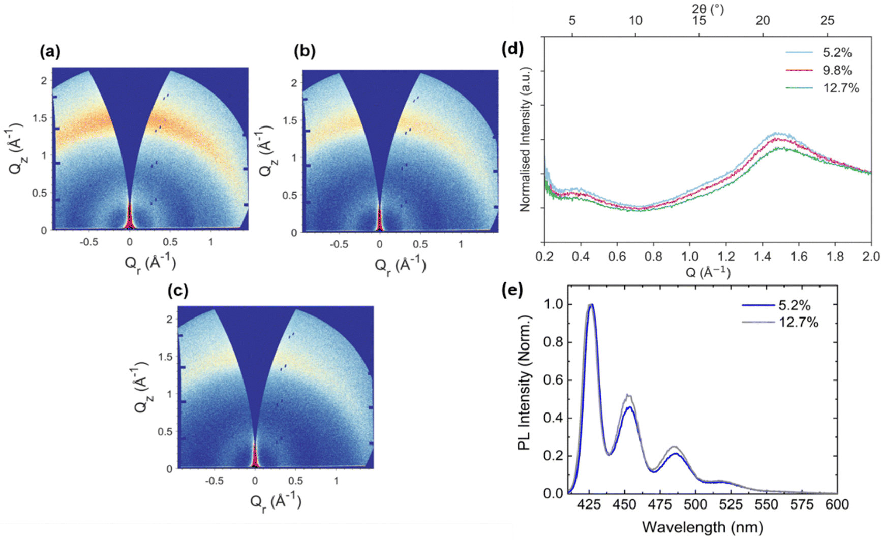 | ||
| Fig. 2 2D GIWAXS patterns of neat BN-PFO films with various binaphthyl (BN) spacer contents of (a) 5.2 mol%, (b) 9.8 mol% and 12.7 mol%. (d) Corresponding normalised 1D azimuthally integrated intensity profiles. The higher BN concentration reduces the β-phase formation in the BN-PFO films. (e) Normalised low temperature PL emission for BN-PFO 5.2 mol% (blue) and 12.7 mol% (grey) at 30K. | ||
Previous work has shown that the inclusion of BN spacer units along the polymer chain suppress the formation of the PFO β-phase.19 However, the PL emission from all the BN-PFO samples explored is characteristic of the α-phase (even at low temperature), suggesting that the β-phase is almost completely absent in the films studied here (see Fig. 2(e)).
To explore how the BN concentration affects the lasing threshold, the threshold from amplified spontaneous emission (ASE) was measured for BN-PFO samples containing 5.2%, 9.8% and 12.7% BN units. Here, ASE originates from the same processes that generate lasing and is therefore a good technique to explore the ability of a material to undergo optical gain. To measure ASE, thin films of BN-PFO at each BN concentration were excited by a Q-switched 355 nm Nd:YAG laser that was focused into a stripe on the surface of the thin films. Fig. 3(a) shows the input vs output characteristics for each BN concentration. In each case, we evidence a fluence at which there is a change of gradient, indicative of a changeover from a spontaneous emission regime to stimulated emission. This change can be clearly seen in Fig. 3(b), with the linewidth of the emission narrowing as stimulated emission dominates. At this point, a sufficient population inversion is created, with net gain exceeding absorptive losses. Fig. 3(c) plots the ASE threshold as a function of BN concentration. Here it can be seen that there is a 1.9 times reduction in ASE threshold between the polymers having the highest and lowest BN concentration. This result is consistent with other reports19 in which similar reductions in lasing threshold are reported for BN-PFO with various concentrations of BN units, where the lower thresholds are attributed to a reduction in β-phase formation. However, we do not believe our films contain any appreciable concentration of β-phase and thus a different explanation is needed. Instead, we suspect that the increased molecular disorder as evidenced by GIWAXS data, together with the ‘dilution’ and conjugation-breaking effects caused by the enhanced BN-fraction inhibits exciton diffusion and thus exciton–exciton interactions that result in the quenching of singlet-excited states that are essential for lasing.
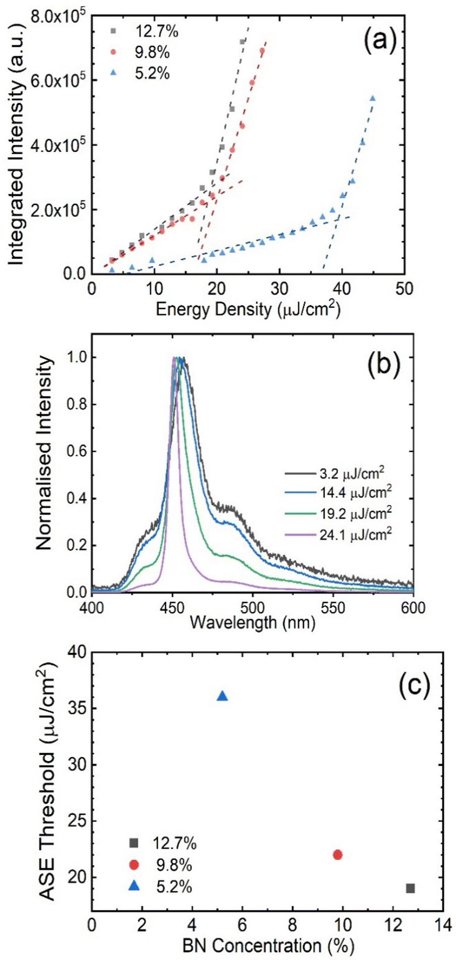 | ||
| Fig. 3 (a) ASE integrated intensity as a function of energy density for BN-PFO with different concentrations of BN (b) BN-PFO (12.7%) ASE spectra linewidth narrowing as pump fluence increases (c) ASE threshold as a function of BN concentration (12.7% = 19 μJ cm−2, 9.8% = 22 μJ cm−2, 5.2% = 36 μJ cm−2). | ||
BN-PFO planar microcavity
Having identified the BN-PFO material with the lowest lasing threshold, we have explored whether we can generate lasing emission by placing it inside a microcavity. The structure of the cavities (without a defect) is shown in Fig. 1(b). The cavity was pumped using a Q-switched 355 nm Nd:YAG laser focused to a spot size having an area of 8.18 × 10⁻⁵ cm−2 at normal incidence. Cavity emission was collected from the top DBR as a function of pump fluence using a Fourier imaging PL dispersion set up in a transmission configuration (see details in experimental section). At low pump fluence the emission measured from the planar cavity at normal incidence is centred at 445 nm, and has a broad angular dependence, having a close to parabolic dispersion as shown in Fig. 4(a). The full width half maxima (FWHM) for all emission spectra were determined by fitting each individual spectrum with a Lorentzian function. From this, we measured an emission linewidth of 0.9 nm, corresponding to a cavity Q-factor (Q = λ/Δλ) of 494; a value comparable to other cavities having a similar structure.55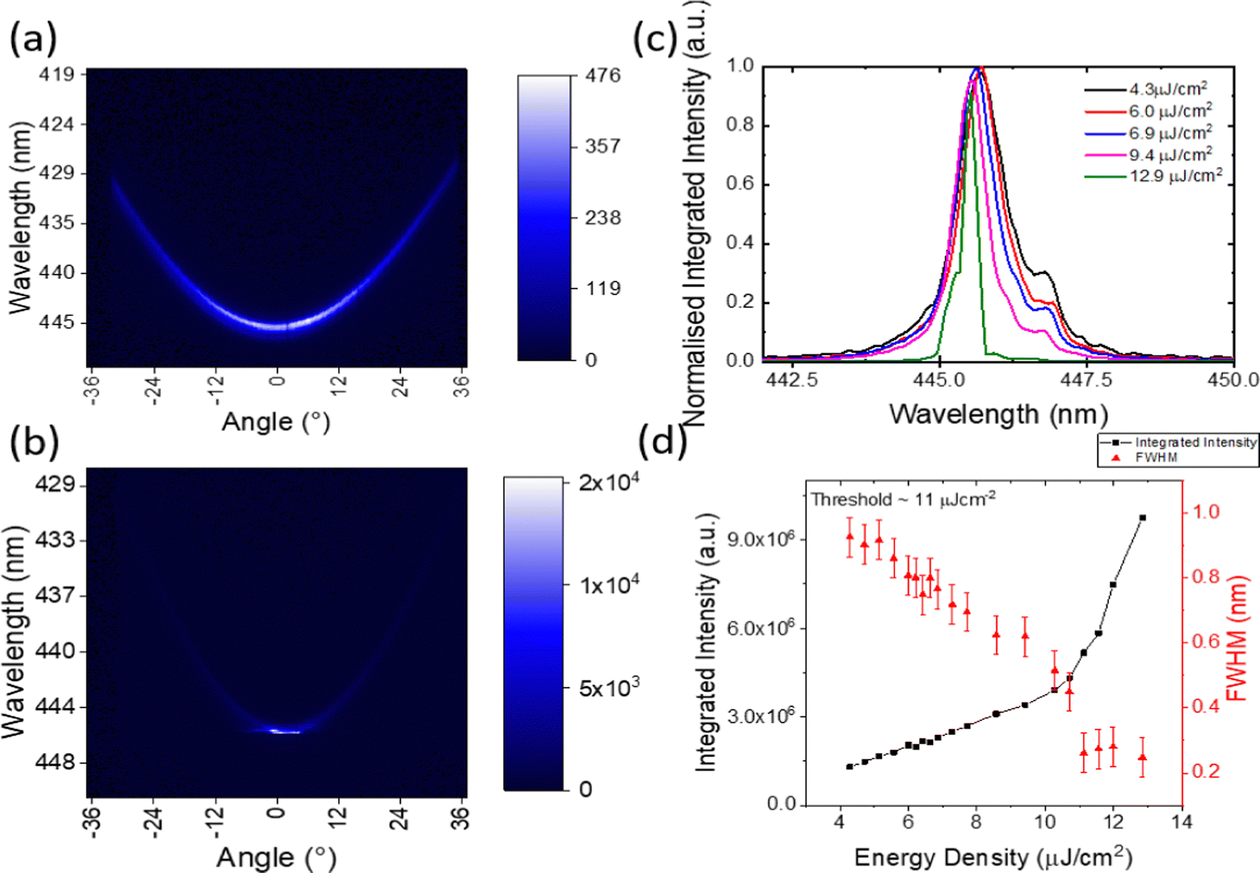 | ||
| Fig. 4 Planar microcavity Fourier imaging PL dispersion (a) below threshold at 6 μJ cm−2 (b) after threshold (11 μJ cm−2) (c) emission spectra narrowing captured at k = 0, as a function of energy density (d) input–output characteristics for planar cavity, where integrated intensity (left) and FWHM (right) is plotted as a function of energy density. | ||
The cavity was then pumped at a range of excitation fluences, with PL emission at normal incidence shown in Fig. 4(b). It can be seen that as the pump fluence is increased, a reduction is observed in the emission linewidth. This can be more clearly seen in Fig. 4(c) where we plot emission linewidth (measured at normal incidence) as a function of pump intensity. Here a discontinuous drop in linewidth is observed at threshold of 11 μJ cm−2, which is lower than previously reported polymer microcavities (84 μJ cm−2 and 17 μJ cm−2).31,56 We suspect that the emission linewidth most likely falls below the resolution of our spectrometer, which we estimate to be 0.2 nm. Nevertheless, we associate this reduction in linewidth with a lasing threshold on the basis of the integrated emission intensity (shown in the same figure) which undergoes a non-linear increase at the same fluence. Notably, we also evidence a significant change in the directionality of emission above lasing threshold. This can be seen in Fig. 4(b) where the emission dispersion is plotted at threshold. Here it can be seen that emission is now concentrated into a tight forward cone having an angular width of 1.5°. This collapse in angular emission direction is again consistent with lasing emission.
BN-PFO defect microcavity
We now discuss the effect of generating a localised defect in a planar microcavity on its emission and lasing properties. A schematic of the defect structure is shown in Fig. 1(b). We have characterised such structures using AFM as shown in Fig. 5(e). Here, measurements were recorded on the patterned PS layer, on a DBR deposited onto the patterned PS layer and finally on the surface of the complete cavity stack. We find that typical defects have a near Gaussian shape, a maximum depth of 40 nm and a diameter of approximately 2.5 μm. Here the diameter of the defects was defined by the beam-waist of the focussed patterning laser on the sample surface, with the depth being chosen to minimise thermally-induced damage to the patterned polystyrene layer. Our measurements indicate that such defects propagate throughout the structure of the microcavity and are not planarized by the BN-PFO film. This modification to the cavity structure results in a relative change in lateral refractive index, effectively providing a 3D confinement that reduces the mode volume.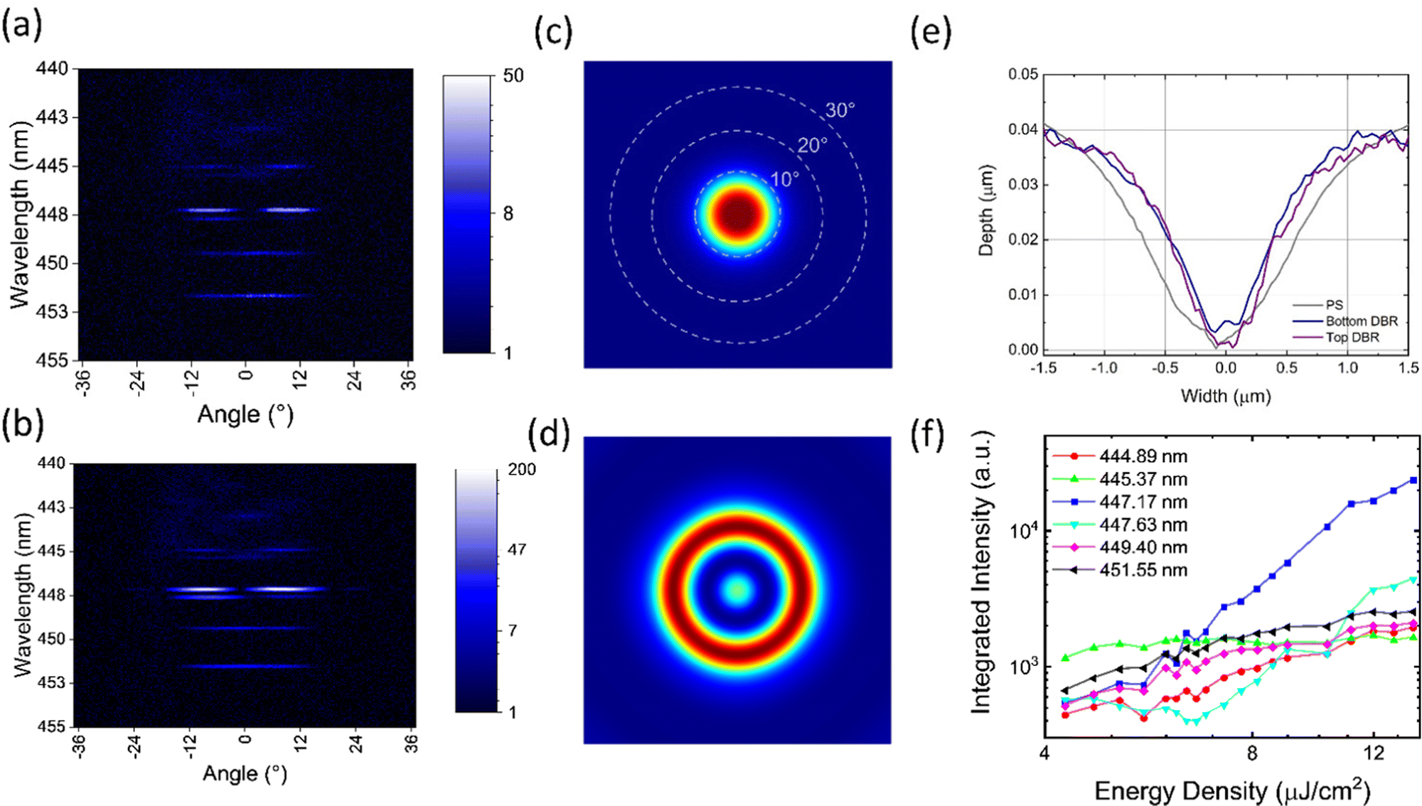 | ||
| Fig. 5 Defect microcavity dispersion (a) below threshold (7.7 μJ cm−2) (b) above threshold (12.0 μJ cm−2), Numerical simulation of the far-field projection for cylindrical defect (c) lowest energy mode (d) lasing mode (e) Defect profile for each layer of the microcavity, measured with AFM (f) Integrated intensity extracted from the Fourier imaging dispersion as a function energy density for each emitting mode with lasing coming from 447.17 nm. | ||
We have used Fourier imaging to characterise emission from single defects both below and above lasing threshold. Here, an additional XY-axis square slit was positioned at the focal length of the imaging lens. This allowed the real space region of the sample to be spatially filtered, allowing only emission from a single defect to be directed to the spectrometer.
An image of emission dispersion below threshold is shown in Fig. 5(a). Here it can be seen that the emission is quantised into a series of modes evident at 444.89, 445.37, 447.17, 447.63, 449.46, and 451.55 nm. It is apparent that the modes at 444.89, 447.17, and 447.63 nm are split into two maxima which are located at angles of −8.4° and 8.4°, and therefore suggest that at this wavelength, emission is emitted into a ‘ring’. Similar mode structures to our defects have also been reported for photonic dots that also effectively reduce the mode volume in a microcavity.34,38
The emission linewidth of the various modes is around 0.2 nm; a value much narrower than the planar cavity linewidth of 0.9 nm. Interestingly, we find that emission from the mode at 447.17 nm is brightest. The estimated Q-factor (below threshold) for this mode is 2300, however this value likely represents a lower bound as the observed emission linewidth is resolution-limited by our spectrometer, which is around 0.2 nm. We believe that the additional lateral confinement from the defect increases the photon lifetime and is responsible for the significant increase in Q-factor. The reduced mode volume (V) and high Q-factor are expected to enhance the rate of spontaneous emission into the lasing mode to reduce the lasing threshold.30
Fig. 5(b) plots the dispersion of cavity emission at a pump fluence of 12.0 μJ cm−2 (above threshold in the planar cavity). Here, it appears that the defect emission is concentrated into a ring-like mode at 447.17 nm. We have used FDTD numerical simulations to describe the structure of selected defect modes. Here the cavity was approximated as a cylindrical defect having a diameter of 2.5 μm and a depth of 40 nm. We plot the far-field projections of the lowest energy mode and the lasing mode in Fig. 5(c) and (d). In both our numerical and experimental measurements, we find that the field projections for these modes have circular symmetry resulting from the structure of the defect.
We find that the majority of the emission comes from the ring-like mode at 447.17 nm, with the other modes being much less intense in emission. We associate this non-linear behaviour with the onset of lasing – a conclusion that is supported by comparing the relative input–output behaviour of the different cavity modes. This is shown in Fig. 5(f), where we plot the integrated intensity of each of the different optical modes as a function of pump fluence. Significantly, we find that the mode at 447.17 nm undergoes a large, non-linear increase in intensity with increasing pump-fluence, whilst the emission from the other modes grows only linearly. We believe that this is clear evidence of a lasing process, with a threshold of 7 μJ cm−2 identified. Note that the mode at 447.63 also undergoes a non-linear increase in intensity, however as the intensity from this mode is comparable to that of the other non-lasing modes, we do not characterise this as lasing. The threshold of 7 μJ cm−2 is comparable to other organic micro lasers that report thresholds of 20 μJ cm−2 using a thermal evaporation shadow mask technique,57 and 4.2 μJ cm−2 with more complicated fabrication involving e-beam lithography and FIB.58 For completeness, Fig. S3 (ESI†) compares the threshold measured here with other polymer laser architectures. We emphasize that the linewidth of the emission was below the resolution of our spectrometer both below and above threshold, and it was therefore not possible to evidence the lasing threshold from changes in mode linewidth alone. We note that the lasing threshold of the defect cavity is 60% of that of the planar cavity (11 μJ cm−2). This indicates that despite the enhanced optical confinement generated by the defect, its effect on optical gain is relatively modest. We suspect this is due to light emission originating from a higher order mode, suggesting that coupling to higher energy modes is less efficient. This has been demonstrated in photonic dots, where higher energy modes have increased lasing thresholds.38 As the lasing emission from our defect is not from the lowest mode, we believe with further optimisation the threshold for our defect cavities can be reduced.
Conclusions
We have explored amplified spontaneous emission (ASE) in films of the co-polymer BN-PFO, and in planar and defect microcavities containing BN-PFO. We firstly demonstrate that by increasing the relative fraction of BN to PFO along the molecular backbone increases molecular disorder. As a result of such enhanced disorder, we are able to reduce the threshold for ASE by 1.9 times to 19 μJ cm−2. We then explore lasing from BN-PFO when placed into a regular planar microcavity, and a microcavity containing a 2.5 μm wide defect that provides additional localisation of the confined optical defect. We show that the presence of the defect results in enhanced optical confinement, with cavity Q-factor increasing from 494 in the planar cavity, to over 2300 in the defect cavity. Lasing was observed in both types of structure, but despite the additional optical confinement, the thresholds for lasing in both types of structure were similar at 7 μJ cm−2 and 11 μJ cm−2 in the defect cavity and planar cavity respectively. The fabrication of such defect structures was achieved using an optical patterning technique that has the potential to be used to write large arrays of defects. Our approach may therefore find potential application in the fabrication of microscale laser devices for integrated photonic circuits and sensors.Author contributions
Experimental characterisation of materials, thin films and microcavities was performed by P. C., R. J., and R. C. K. under the supervision of D. G. L. BN-PFO was synthesized by T. J. under the supervision of U.S. Data visualisation was performed by P. C. and assisted by T. T. and R. D. J. O. Numerical simulations was calculated by A. M. The manuscript was written by P. C., R. C. K., A. M. A. and D. G. L., with all other authors contributing to its final version.Conflicts of interest
D. G. L. is co-founder and Chairman of the company Ossila Ltd which retails materials and equipment used in materials science research, including conjugated polymers and equipment used to process and characterise thin films.Acknowledgements
We thank the U.K. EPSRC for funding this work via the Programme Grant ‘Hybrid Polaritonics’ (EP/M025330/1). P. C. thanks the Universities of Sheffield and Hull for co-funding his PhD studentship. The authors also acknowledge the EPSRC for the capital equipment grants to purchase (EP/M028437/1) and upgrade (EP/V034804/1) the laboratory-based Xenocs/Excillum X-ray scattering instrument.References
- C. A. M. Senevirathne, A. S. D. Sandanayaka, B. S. B. Karunathilaka, T. Fujihara, F. Bencheikh, C. Qin, K. Goushi, T. Matsushima and C. Adachi, ACS Photonics, 2021, 8, 1324–1334 CrossRef CAS.
- F. Chen, D. Gindre and J.-M. Nunzi, Opt. Express, 2008, 16, 16746 CrossRef PubMed.
- L. Zhou, M. Yu, X. Chen, S. Nie, W.-Y. Lai, W. Su, Z. Cui and W. Huang, Adv. Funct. Mater., 2018, 28, 1705955 CrossRef.
- C. Yan, Y. Liu, W. Yang, J. Wu, X. Wang and L. Liao, Angew. Chem., Int. Ed., 2022, 61, e202210422 CAS.
- J. Wu, M. Zhuo, R. Lai, S. Zou, C. Yan, Y. Yuan, S. Yang, G. Wei, X. Wang and L. Liao, Angew. Chem., Int. Ed., 2021, 133, 9196–9201 CrossRef.
- W. Yang, R. Lai, J. Wu, Y. Yu, C. Yan, C. Sun, X. Wang and L. Liao, Adv. Funct. Mater., 2022, 32, 2204129 CrossRef CAS.
- A. Rose, Z. Zhu, C. F. Madigan, T. M. Swager and V. Bulović, Nature, 2005, 434, 876–879 CrossRef CAS PubMed.
- Y. Su, B. Wu, S. Chen, J. Sun, Y. Yu, M. Zhuo, Z. Wang and X. Wang, Angew. Chem., Int. Ed., 2022, 61, e202117857 CAS.
- C. Vannahme, S. Klinkhammer, U. Lemmer and T. Mappes, Opt. Express, 2011, 19, 8179 CrossRef CAS PubMed.
- J. Clark and G. Lanzani, Nat. Photonics, 2010, 4, 438–446 CrossRef CAS.
- A. S. D. Sandanayaka, T. Matsushima, F. Bencheikh, S. Terakawa, W. J. Potscavage, C. Qin, T. Fujihara, K. Goushi, J.-C. Ribierre and C. Adachi, Appl. Phys. Express, 2019, 12, 061010 CrossRef CAS.
- Q. Zhang, W. Tao, J. Huang, R. Xia and J. Cabanillas-Gonzalez, Adv. Photonics Res., 2021, 2, 2000155 CrossRef.
- C. Gärtner, C. Karnutsch, U. Lemmer and C. Pflumm, J. Appl. Phys., 2007, 101, 023107 CrossRef.
- A. S. D. Sandanayaka, K. Yoshida, M. Inoue, C. Qin, K. Goushi, J. C. Ribierre, T. Matsushima and C. Adachi, Adv. Opt. Mater., 2016, 4, 834–839 CrossRef CAS.
- T. Rabe, K. Gerlach, T. Riedl, H.-H. Johannes, W. Kowalsky, J. Niederhofer, W. Gries, J. Wang, T. Weimann, P. Hinze, F. Galbrecht and U. Scherf, Appl. Phys. Lett., 2006, 89, 081115 CrossRef.
- A. S. D. Sandanayaka, L. Zhao, D. Pitrat, J.-C. Mulatier, T. Matsushima, C. Andraud, J.-H. Kim, J.-C. Ribierre and C. Adachi, Appl. Phys. Lett., 2016, 108, 223301 CrossRef.
- H. Nakanotani, C. Adachi, S. Watanabe and R. Katoh, Appl. Phys. Lett., 2007, 90, 4–7 Search PubMed.
- B. K. Yap, R. Xia, M. Campoy-Quiles, P. N. Stavrinou and D. D. C. Bradley, Nat. Mater., 2008, 7, 376–380 CrossRef CAS PubMed.
- T. Rabe, M. Hoping, D. Schneider, E. Becker, H.-H. Johannes, W. Kowalsky, T. Weimann, J. Wang, P. Hinze, B. S. Nehls, U. Scherf, T. Farrell and T. Riedl, Adv. Funct. Mater., 2005, 15, 1188–1192 CrossRef CAS.
- M. Meier, A. Mekis, A. Dodabalapur, A. Timko, R. E. Slusher, J. D. Joannopoulos and O. Nalamasu, Appl. Phys. Lett., 1999, 74, 7–9 CrossRef CAS.
- D. Lin, J. Liu, H. Zhang, Y. Qian, H. Yang, L. Liu, A. Ren, Y. Zhao, X. Yu, Y. Wei, S. Hu, L. Li, S. Li, C. Sheng, W. Zhang, S. Chen, J. Shen, H. Liu, Q. Feng, S. Wang, L. Xie and W. Huang, Adv. Mater., 2022, 34, 2109399 CrossRef CAS PubMed.
- H. Kogelnik and C. V. Shank, Appl. Phys. Lett., 1971, 18, 152–154 CrossRef CAS.
- D. Lin, Y. Li, H. Zhang, S. Zhang, Y. Gao, T. Zhai, S. Hu, C. Sheng, H. Guo, C. Xu, Y. Wei, S. Li, Y. Han, Q. Feng, S. Wang, L. Xie and W. Huang, Research, 2023, 6, 1–12 CrossRef.
- N. Tessler, G. J. Denton and R. H. Friend, Nature, 1996, 382, 695–697 CrossRef CAS.
- X. Lu, X. Wang, Q. Liao and H. Fu, J. Phys. Chem. C, 2015, 119, 22108–22113 CrossRef CAS.
- H.-T. Lin, Y.-X. Ma, S. Chen and X.-D. Wang, Angew. Chem., Int. Ed., 2023, 62, e202214214 CAS.
- S. Morimura and K. Ujihara, Japn. J. Appl. Physics, Part 1 Regul. Pap. Short Notes Rev. Pap., 1997, 36, 4307–4311 CrossRef CAS.
- Y. Hu, J. Lin, L. Song, Q. Lu, W. Zhu and X. Liu, Sci. Rep., 2016, 6, 23210 CrossRef CAS PubMed.
- Y. Hu, F. Bencheikh, S. Chénais, S. Forget, X. Liu and C. Adachi, Appl. Phys. Lett., 2020, 117, 153301 CrossRef CAS.
- F. P. L. Alexey, V. Kavokin, J. J. Baumberg and G. Malpuech, Microcavities, Oxford Science Publications, 2nd edn, 2017 Search PubMed.
- L. Persano, P. Del Carro, E. Mele, R. Cingolani, D. Pisignano, M. Zavelani-Rossi, S. Longhi and G. Lanzani, Appl. Phys. Lett., 2006, 88, 121110 CrossRef.
- A. M. Adawi, A. Cadby, L. G. Connolly, W.-C. Hung, R. Dean, A. Tahraoui, A. M. Fox, A. G. Cullis, D. Sanvitto, M. S. Skolnick and D. G. Lidzey, Adv. Mater., 2006, 18, 742–747 CrossRef CAS.
- R. Brückner, A. A. Zakhidov, R. Scholz, M. Sudzius, S. I. Hintschich, H. Fröb, V. G. Lyssenko and K. Leo, Nat. Photonics, 2012, 6, 322–326 CrossRef.
- D. Urbonas, T. Stöferle, F. Scafirimuto, U. Scherf and R. F. Mahrt, ACS Photonics, 2016, 3, 1542–1545 CrossRef CAS.
- F. L. Al-Jashaam, R. Jayaprakash, D. M. Coles, A. J. Musser, K. Georgiou and D. G. Lidzey, Adv. Quantum Technol., 2020, 3, 1900067 CrossRef CAS.
- F. Ding, T. Stöferle, L. Mai, A. Knoll and R. F. Mahrt, Phys. Rev. B: Condens. Matter Mater. Phys., 2013, 87, 161116 CrossRef.
- L. Mai, F. Ding, T. Stöferle, A. Knoll, B. Jan Offrein and R. F. Mahrt, Appl. Phys. Lett., 2013, 103, 243305 CrossRef.
- M. Langner, M. Sudzius, S. I. Hintschich, H. Fröb, V. G. Lyssenko and K. Leo, in Organic Optoelectronics and Photonics III, ed. P. L. Heremans, M. Muccini and E. A. Meulenkamp, 2008, vol. 6999, p. 699902 Search PubMed.
- R. Jayaprakash, C. E. Whittaker, K. Georgiou, O. S. Game, K. E. McGhee, D. M. Coles and D. G. Lidzey, ACS Photonics, 2020, 7, 2273–2281 CrossRef CAS.
- M. Lehnhardt, T. Riedl, U. Scherf, T. Rabe and W. Kowalsky, Org. Electron., 2011, 12, 1346–1351 CrossRef CAS.
- C. Karnutsch, C. Gýrtner, V. Haug, U. Lemmer, T. Farrell, B. S. Nehls, U. Scherf, J. Wang, T. Weimann, G. Heliotis, C. Pflumm, J. C. DeMello and D. D. C. Bradley, Appl. Phys. Lett., 2006, 89, 201108 CrossRef.
- T. Wellinger, C. Pflumm, J. Becker, T. Weimann, M. Campoy-Quiles, P. N. Stavrinou, U. Scherf and D. D. C. Bradley, in Organic Optoelectronics and Photonics III, ed. P. L. Heremans, M. Muccini and E. A. Meulenkamp, 2008, vol. 6999, p. 699907 Search PubMed.
- Z. Jiang, J. Appl. Crystallogr., 2015, 48, 917–926 CrossRef CAS.
- W. C. Tsoi and D. G. Lidzey, J. Phys.: Condens. Matter, 2008, 20, 125213 CrossRef.
- M. Grell, D. D. C. Bradley, G. Ungar, J. Hill and K. S. Whitehead, Macromolecules, 1999, 32, 5810–5817 CrossRef CAS.
- P. Wilhelm, D. Blank, J. M. Lupton and J. Vogelsang, ChemPhysChem, 2020, 21, 961–965 CrossRef CAS PubMed.
- M. Misaki, S. Nagamatsu, M. Chikamatsu, Y. Yoshida, R. Azumi, N. Tanigaki, Y. Ueda and K. Yase, Polym. J., 2007, 39, 1306–1311 CrossRef CAS.
- M. Ariu, D. G. Lidzey, M. Sims, A. J. Cadby, P. A. Lane and D. D. C. Bradley, J. Phys.: Condens. Matter, 2002, 14, 9975–9986 CrossRef CAS.
- A. L. T. Khan, P. Sreearunothai, L. M. Herz, M. J. Banach and A. Köhler, Phys. Rev. B: Condens. Matter Mater. Phys., 2004, 69, 085201 CrossRef.
- A. Perevedentsev, Y. Sonnefraud, C. R. Belton, S. Sharma, A. E. G. Cass, S. A. Maier, J.-S. Kim, P. N. Stavrinou and D. D. C. Bradley, Nat. Commun., 2015, 6, 5977 CrossRef CAS PubMed.
- A. Perevedentsev, N. Chander, J. S. Kim and D. D. C. Bradley, J. Polym. Sci., Part B: Polym. Phys., 2016, 54, 1995–2006 CrossRef CAS PubMed.
- M. E. Caruso and M. Anni, Phys. Rev. B: Condens. Matter Mater. Phys., 2007, 76, 054207 CrossRef.
- S. H. Chen, A. C. Su and S. A. Chen, J. Phys. Chem. B, 2005, 109, 10067–10072 CrossRef CAS PubMed.
- G. C. Faria, T. S. Plivelic, R. F. Cossiello, A. A. Souza, T. D. Z. Atvars, I. L. Torriani and E. R. DeAzevedo, J. Phys. Chem. B, 2009, 113, 11403–11413 CrossRef CAS PubMed.
- K. E. McGhee, R. Jayaprakash, K. Georgiou, S. L. Burg and D. G. Lidzey, J. Mater. Chem. C, 2022, 10, 4187–4195 RSC.
- A. Palatnik and Y. R. Tischler, IEEE Photonics Technol. Lett., 2016, 28, 1823–1826 CAS.
- M. Sudzius, M. Langner, S. I. Hintschich, V. G. Lyssenko, H. Fröb and K. Leo, Appl. Phys. Lett., 2009, 94, 061102 CrossRef.
- P. B. Deotare, T. S. Mahony and V. Bulović, ACS Nano, 2014, 8, 11080–11085 CrossRef CAS PubMed.
Footnote |
| † Electronic supplementary information (ESI) available. See DOI: https://doi.org/10.1039/d2tc05360h |
| This journal is © The Royal Society of Chemistry 2023 |