
 Open Access Article
 This Open Access Article is licensed under a Creative Commons Attribution-Non Commercial 3.0 Unported Licence
Molecularly engineered host materials for high performance inkjet-printed thermally activated delayed fluorescence organic light-emitting diodes†
Honghui
Wei
ab,
Yuan-Qiu-Qiang
Yi
 *b,
Yanping
Song
a,
Liming
Xie
b,
Yang
Liu
b,
Zhipeng
Wei
c,
Qian
Dai
d,
Xiuqing
Meng
*a,
Wenming
Su
b and
Zheng
Cui
b
*b,
Yanping
Song
a,
Liming
Xie
b,
Yang
Liu
b,
Zhipeng
Wei
c,
Qian
Dai
d,
Xiuqing
Meng
*a,
Wenming
Su
b and
Zheng
Cui
b
aCollege of Physics and Electronic Information Engineering, Zhejiang Normal University, Jinhua, 321004, Zhejiang, China. E-mail: xqmeng@zjnu.cn
bPrintable Electronics Research Center, Nano Devices and Materials Division, Suzhou Institute of Nano-Tech and Nano-Bionics, Chinese Academy of Sciences, Suzhou 215123, Jiangsu, China. E-mail: yqqyi2020@sinano.ac.cn
cState Key Laboratory of High Power Semiconductor Lasers, Changchun University of Science and Technology, Changchun, 130022, P. R. China
dSouthwest Institute of Technical Physics, Chengdu, 610041, P. R. China
First published on 17th March 2023
Abstract
Due to the low cost and high performance of thermally activated delayed fluorescence (TADF) materials, TADF based organic light-emitting diodes (OLEDs) are highly attractive for future display panels. To improve the material usage and direct pixelation, inkjet printing (IJP) is deemed as one of the most potential technologies for fabricating large-area and flexible OLEDs, which requires the materials to be solution processable and inkjet printable. However, there are only a few host materials with appropriate thermal stability and solution processability to meet the requirements for IJP fabrication of OLEDs. Herein, three new host materials for solution-processed OLEDs have been designed and synthesized with different molecular symmetries by molecularly engineering the widely used 4,4′-bis(9-carbazolyl)-2,2′-biphenyl (CBP), named AC1, AC2, and AC3. Among them, AC2 and AC3 showed comparatively high thermal stability. Spin-coating processed TADF-OLEDs (4CzIPN as the emitter) based on the three hosts have been fabricated, and the AC2-based TADF-OLED exhibited the highest maximum external quantum efficiency (EQE) of 16.4%. Its IJP fabricated device also achieved a maximum EQE of 11.0%, which is the highest among reported TADF-OLEDs by IJP fabrication.
Introduction
Since the pioneering work of Tang and coworker in 1987, organic light-emitting diodes (OLEDs) have witnessed three-generation developments from fluorescence1,2 through phosphorescence2–5 to thermally activated delayed fluorescence (TADF).6,7 TADF, the third-generation OLED technology, is normally based on organic emitters,8 which can upconvert an exciton from the triplet state to the singlet state via reverse intersystem crossing.9,10 TADF-based OLEDs have aroused great enthusiasm within the OLED research community, mainly due to their metal-free nature and ability to harvest both singlet and triplet excitons.7 However, to date, TADF-based OLEDs have been mainly fabricated by vacuum deposition processes.11,12 Compared to vacuum-processing techniques, which are limited by poor material yield and insufficient thickness homogeneity on large substrates,13–15 solution-processing techniques are more competitive in low-cost and large-scale OLED fabrication.14,16–19 Among various solution-processing techniques, inkjet printing (IJP) is of great interest, especially in the display industry, for its high material utilization, accurate deposition, and direct patternability.20–24Even though huge successes have been achieved in vacuum deposited TADF-OLEDs, the device performance of solution-processed,25–29 especially inkjet-printed (Table S1, ESI†), TADF-OLEDs still lags far behind their vacuum-processed counterparts.30–33 Many existing challenges can be accountable for the unsuccessful IJP TADF-OLEDs, such as the lack of solution-processed materials, unsuitable ink formula, immature fabrication process and so on. Among them, the lack of suitable solution-processed materials along with unsuccessful ink formula has impeded the desired film formation in IJP TADF-OLEDs.34 As such, extensive research studies have focused on highly soluble materials to improve their film formation ability.33 According to the film-formation mechanism of solution-processing techniques, self-hosted TADF might be a more reliable way to construct an efficient OLED device. However, it is difficult to design a TADF organic molecule with balanced and high carrier transport ability.35–37 Similar to the approach in phosphorescent OLEDs, highly efficient TADF-OLEDs can be fabricated by dispersing the TADF emitter into a host matrix.38–40 A suitable host should have not only a high triplet energy to prevent triplet–triplet annihilation, but also appropriate energy levels to facilitate efficient exciton generation.38 Unfortunately, most of the developed host materials were specifically designed for vacuum-processed OLEDs and are not compatible with solution-processed TADF-OLEDs.38 As a key component in the emissive layer (EML), the host material bears a major responsibility for the solution processability and film formation quality. The lack of progress in solution processible host materials mainly originates from their low glass-transition temperature and poor solubility, rendering them unsuitable candidates for IJP TADF-OLEDs.
In the present work, three new host materials named AC1, AC2, and AC3 have been designed and synthesized by molecularly engineering the widely used 4,4′-bis(9-carbazolyl)-2,2′-biphenyl (CBP).41–43 The three host materials share almost the same molecular size but vary in symmetries. As shown in Fig. 1, AC1 is end-capped with four ethyl groups on both carbazole units, while AC2 introduces only two tertiary butyl (tBu) groups on one carbazole unit. AC3 shifts its conjugation linking position to the C-3 position of another carbazole. Although polymers based on the AC2 structure have been reported to have a high triplet energy as a host material,44 it is still necessary to study whether the AC2 molecule is a suitable host for solution-processed EMLs. The physical properties of the three host materials were studied in detail. It was found that AC2 and AC3 showed obvious improvements in thermal stability and solubility compared to symmetric host AC1. The highly efficient TADF emitter 4CzIPN45,46 has been utilized to fabricate TADF-OLEDs by both spin-coating and IJP. Owing to its high thermal stability (Tg = 135 °C), the spin-coated device based on AC2 showed a high external quantum efficiency (EQE) of 16.4%. By formulating AC2 and 4CzIPN into a reported solvent, butyl benzoate,47–49 as an ink, an IJP device has also been successfully fabricated with an EQE of 11.0%, representing the highest among reported organic TADF-OLEDs by IJP fabrication.
 | ||
| Fig. 1 Molecular structures, the HOMO distribution, calculated electrostatic potential (ESP) mapping profiles and surface area in each ESP range (per 2.5 kcal mol−1).16,53 | ||
Experimental section
Materials
AC1 and AC3 were both synthesized by a one-step procedure, and the detailed synthetic procedures are shown in the ESI.†AC2 was obtained by customized synthesis from Suzhou OPQ Display, Inc. Chlorobenzene and octane were purchased from Sigma-Aldrich Ltd. Indium tin oxide (ITO) substrates and PEDOT:PSS (AI4083, Clevios™) were purchased from Jingzhitai Optoelectronic Technology Corp. and Heraeus, respectively. 4CzIPN was purchased from Xi’an Polymer Light Technology Corp. TPBi and Liq were purchased from Shanghai Hanfeng.Fabrication of OLED devices
The ITO substrate was washed with a glass cleaner (Y-25, Shanghai Yuanyu Chemical Technology Co., Ltd), then ultrasonicated with deionized water and ethanol, and finally treated with oxygen plasma for 5 min. PEDOT:PSS (AI4083, Clevios™, Heraeus, Germany) was spin-coated on an ITO substrate at 4000 rpm for 40 s. Then the coated ITO substrate was transferred to a nitrogen-filled glovebox and baked at 130 °C for 15 min to remove residual solvent.For the spin-coated device, the AC1, AC2, and AC3 host materials blended with the 4CzIPN (Xi’an Polymer Light Technology Corp.) dopant were dissolved in chlorobenzene, then deposited on a PEDOT:PSS layer by spin-coating at 3000 rpm for 30 s and then baked at different annealing temperatures for 20 min. The concentration of EML solutions was used to change the thickness of the EML.
For the inkjet-printed device, AC2 doped with 4CzIPN (8 wt%) was dissolved in butyl benzoate to afford the EML ink with a concentration of 8 mg mL−1. A commercial Fujifilm Dimatix DMP 2831 piezoelectric drop-on-demand inkjet printer, equipped with a 10 pL cartridge in ambient air, was used to print the EML solution onto the PEDOT:PSS layer. Then the substrates were transferred into a nitrogen-filled glovebox and baked at 100 °C for 20 min.
The following fabrication processes of the spin-coated or inkjet-printed device are the same. The samples were transferred to the vacuum evaporation equipment. TPBi, Liq (both from Shanghai Hanfeng Chemical Co.) and Al were deposited sequentially under a vacuum of 2 × 10⁻⁴ mbar at rates of 1 Å s−1, 0.1 Å s−1 and 3 Å s−1, respectively. A mask was used during Al evaporation to afford the OLED with a 2 × 2 mm2 light-emitting area.
Characterization and Device Measurement
UV/vis absorption and room temperature photoluminescence (PL) emission spectra were recorded using a PerkinElmer Lambda 750 and a HITACHI F4600 fluorescence spectrophotometer, respectively. Thermogravimetric analysis (TGA) and differential scanning calorimetry (DSC) curves were recorded using a Mettler TGA/DSC 3+ at a heating rate of 10 °C min−1 under a nitrogen atmosphere. The film surface morphology was recorded using atomic force microscopy (AFM, Veeco Dimension 3100 in the tapping mode). Ultraviolet photoelectron spectroscopy (UPS) was conducted using a PHI 5000 VersaProbe II @Nano-X, with an unfiltered HeI (21.22 eV) gas discharge lamp and a sample bias of 10 V. PR655 was used to measure electroluminescence spectra. A computer-controlled Keithley 2400 source meter was used to characterize current–voltage (I–V) and luminance–voltage (L–V) relationships. The contact angle was recorded by using an SL150L optical contact angle and interface tension meter.Results and discussion
Molecular design and simulation
CBP (4,4′-bis(9-carbazolyl)-2,2′-biphenyl) is a widely used molecule in vacuum-deposited OLEDs because of its excellent hole transport performance.50–52 However, the low Tg (62 °C43) of CBP renders it not suitable for solution-processed OLEDs which requires post-annealing, resulting in a deteriorated film state. To overcome this shortcoming, the present work introduced different alkyl substitutes onto the CBP core, which can not only elevate its Tg but also further enhance its solution processability so that a working ink can be formulated. The three new host materials, AC1, AC2 and AC3, have been designed and synthesized and their molecular structures are shown in Fig. 1. AC1 is end-capped with four ethyl groups on both carbazole units, while AC2 introduces only two tertiary butyl (tBu) groups on one carbazole unit. Different from AC2, AC3 shifts its conjugation linking position to the C-3 position of another carbazole.To validate the design strategy, density functional theory (DFT) calculations were performed using the Gaussian 16 program at the B3LYP/6-31G(d,p) level. As depicted in Fig. 1, the calculated HOMOs of AC1 and AC2 are distributed evenly along the conjugated biphenyl and carbazole units, while the HOMO of AC3 does not display uniform distribution and is mainly located at the carbazole moiety with two t-butyl substituents in C-3 and C-6 positions. The calculated HOMO and LUMO energy levels of AC1, AC2 and AC3 are −5.55/−5.78/−5.59 eV and −2.11/−2.30/−2.10 eV, respectively. Compared to AC1 and AC2, AC3 showed a different electrostatic potential (ESP) distribution with a more electronegative state in the t-butyl carbazole moiety. The optimized molecular structures, HOMO-1 and LUMO of AC1, AC2 and AC3 are summarized in the ESI.†
Physical properties
The thermal properties of AC1, AC2 and AC3 were investigated by using thermogravimetric analysis (TGA) and differential scanning calorimetry (DSC) in nitrogen ambience. The decomposition temperatures of AC1, AC2 and AC3 at 5% weight loss are 418, 419, and 417 °C, respectively, as shown in Fig. 2(a). Because of the two bulky and rigid t-butyl substituents, AC2 and AC3 are found to have higher glass transition temperatures (Tg) of 135 and 125 °C compared to CBP, whereas AC1 shows only a slight increase in Tg (79 °C). The UV-vis absorption and photoluminescence (PL) spectra of the three host materials at room temperature are shown in Fig. 2(b). According to the onset of the UV-vis absorption spectrum, the optical energy gaps (Eg) of AC1, AC2 and AC3 are determined to be around 3.40 eV because of their similar structural moieties. They also share a similar fluorescence spectrum, with a peak value around 380 nm. Ultraviolet photoelectron spectroscopy (UPS) was used to probe their electronic band structures. AC1 (−5.55 eV) has a similar HOMO to AC3 (−5.59 eV), while AC2 exhibits a deeper HOMO of −5.78 eV. The detailed thermal and electrochemical parameters of the three materials are summarized in Table 1.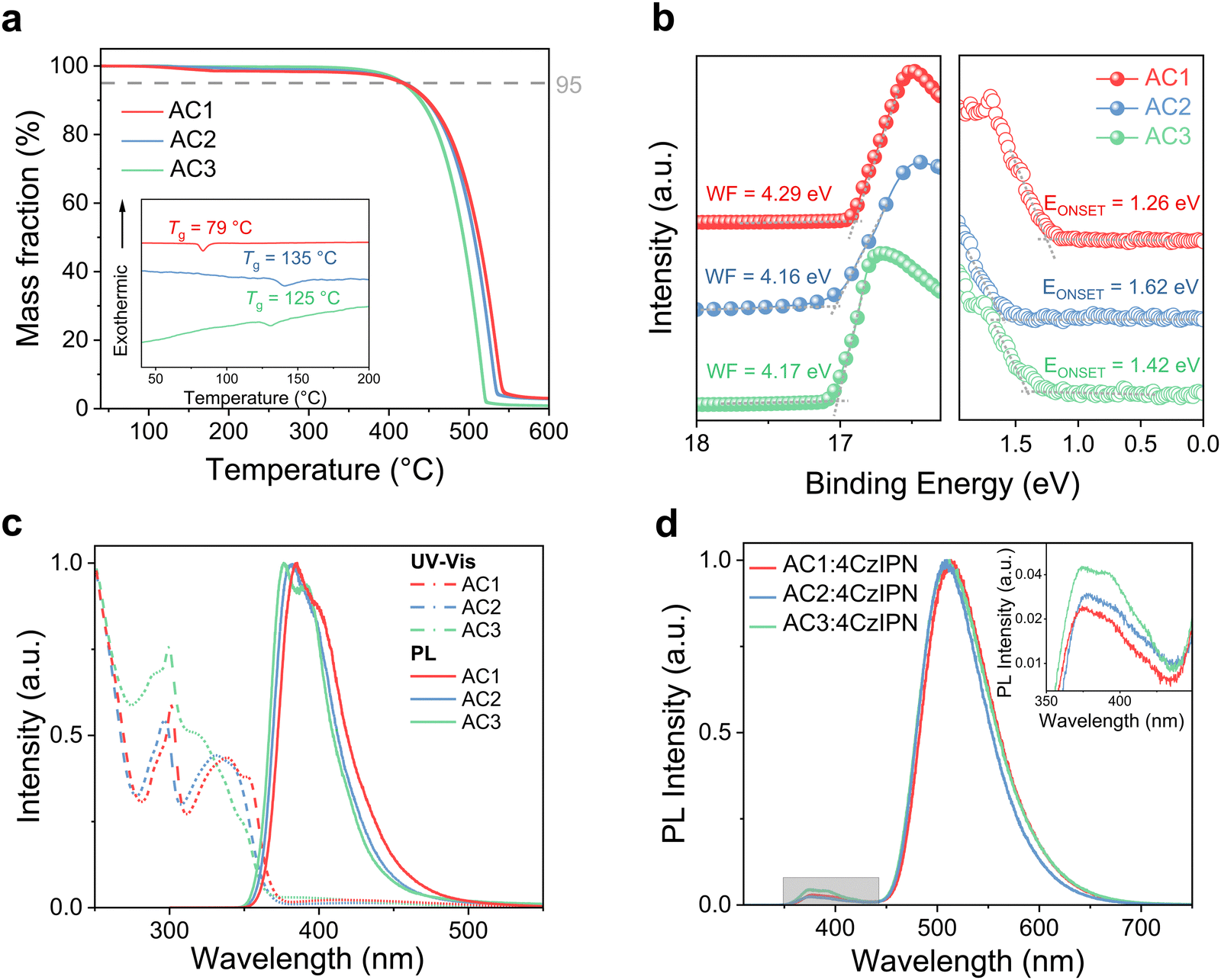 | ||
| Fig. 2 (a) TGA curves of AC1, AC2 and AC3. Inset: DSC trace. (b) UPS spectra of AC1, AC2 and AC3. (c) UV–vis absorption (dotted line) of AC1, AC2 and AC3 at room temperature in dichloromethane and PL as in their neat films (solid line). (d) Photoluminescence spectra of AC1, AC2 and AC3 doped with 8 wt% 4CzIPN in neat films. Inset: 350–450 nm. | ||
| T g (°C) | T d (°C) | E g (eV) | HOMOb (eV) | LUMOc (eV) | HOMOd (eV) | LUMOd (eV) | |
|---|---|---|---|---|---|---|---|
| a Determined from the corresponding absorption onset. b Calculated from UPS, according to the equation of HOMO = Ephoton − (ESE − EONSET) = WF + EONSET. c Calculated according to the equation of LUMO = Eg + HOMO. d Calculated at the B3LYP/6-31G(d,p) level using Gaussian 16. | |||||||
| AC1 | 79 | 418 | 3.44 | −5.55 | −2.11 | −5.14 | −1.16 |
| AC2 | 135 | 419 | 3.48 | −5.78 | −2.30 | −5.20 | −1.19 |
| AC3 | 125 | 417 | 3.49 | −5.59 | −2.10 | −5.04 | −0.85 |
To study the energy transfer from the host materials to the emitter, the PL spectra of AC1, AC2 and AC3 doped with 4CzIPN (8 wt%) were measured and are shown in Fig. 2(d). AC1, AC2 and AC3 doped with 4CzIPN all show a minor emission peak in the range of 350–440 nm. In contrast, AC3 has a comparatively strong emission intensity in this region, which indicates that the energy transfer from AC3 to 4CzIPN is less efficient than that from AC1 and AC2.
Thin-film morphology is of great significance for obtaining highly efficient solution-processed OLEDs. Thus, the contact angles of EML solution on the PEDOT:PSS layer were measured as the wettability of the EML solution would significantly affect their morphologies. As shown in Fig. 3(a), the EML solutions with different hosts all exhibit small contact angles on PEDOT:PSS with values of 6.50, 6.23 and 5.50°, respectively. These results indicate that EML solutions based on all three hosts can spread well on PEDOT:PSS. Atomic force microscopy (AFM) was used to characterize the surface morphologies of the three coated EML films. The AFM height images of the three EML films are shown in Fig. 3(b) and (c). The spin-coated EML films with different hosts show comparable small average roughness values (0.36 nm, 0.35 nm and 0.35 nm for AC1, AC2 and AC3) and similar surface depth distributions. These results together demonstrate that the three hosts are all highly applicable in solution-processed OLEDs.
 | ||
| Fig. 3 (a) Contact angles of AC1, AC2 and AC3 doped with 8 wt% 4CzIPN chlorobenzene solution on the PEDOT:PSS layer. (b) AFM topographic images and three-dimensional images (4 × 4 μm2) of AC1, AC2 and AC3 films doped with 8 wt% 4CzIPN. (c) Surface depth histograms of the EML with different hosts obtained from AFM height images. | ||
Solution-processed OLEDs
To demonstrate their applicability in solution-processed OLEDs, a series of green TADF OLED devices were fabricated by spin-coating using AC1, AC2 and AC3 as the hosts. The device structure was ITO/PEDOT:PSS (30 nm)/4CzIPN:host/TPBi (35 nm)/Liq (2 nm)/Al (200 nm), as illustrated in Fig. 4(a). Different layer thicknesses, doping ratios and annealing temperatures of the EML were investigated. The EL performances of these devices are summarized in Fig. S4–S6 and Tables S3–S5 (ESI†). The devices with their best EL performances shared the same thickness and annealing temperature of the EML (30 nm and 70 °C). Regarding the doping ratio of the host, AC3 with 6 wt% 4CzIPN displayed its best EL performance, while AC1 and AC2 required higher doping ratios (8 wt%) of 4CzIPN in the EML for achieving their best device performance. The current density–voltage–luminance (J–V–L), external quantum efficiency–luminance (EQE–L) and current efficiency–luminance–power efficiency (CE–L–PE) relationships of the optimized devices with AC1, AC2 and AC3 hosts are shown in Fig. 4(d)–(f), and their characteristic parameters are summarized in Table 2. Among them, the AC2 based OLED exhibits the best device performance with the highest EQE, PE and CE of 16.4%, 40.3 lm W−1 and 51.3 cd A−1, respectively. The AC1 based OLED shows an inferior EL performance (EQE = 14.8%, PE = 39.4 lm W−1, CE = 47.6 cd A−1), and the AC3 based OLED showed the worst performance with an EQE of only 10.8%. It is worth noting that an undesirable emission peak appears at 400 nm in the EL spectra of the different host-based OLEDs, which indicates that some of the excited hosts cannot transfer energy efficiently to the emitter before its radiation. | ||
| Fig. 4 (a) Device structure and (b) energy level of the fabricated OLEDs. (c) The CIE 1931 coordinates of optimized OLEDs under a luminance of 1000 cd m−2. (d) J–V–L, (e) EQE, and (f) CE–L–PE of optimized OLEDs with AC1, AC2 and AC3 as hosts. EL spectra of OLEDs at different driving voltages with 8 wt% 4CzIPN doped in AC1 (g), AC2 (h) and AC3 (i). | ||
| Device (host) | EQEa (%) | PEa (lm W−1) | CEa (cd A−1) | L max (cd m−2)b | V T (V) | V D (V) @102, 103, 104 cd m−2 | CIEd (x,y) | |||||
|---|---|---|---|---|---|---|---|---|---|---|---|---|
| a Data at maximum and 1000 cd m−2 from left to right. b Maximum luminance. c Voltage at 1 cd m−2. d CIE: Commission Internationale de I’Eclairage at 1000 cd m−2. | ||||||||||||
| AC1 | 14.8 | 13.0 | 39.4 | 27 | 47.6 | 41 | 9868 | 3.1 | 4.1 | 4.9 | — | (0.32,0.56) |
| AC2 | 16.4 | 14.5 | 40.3 | 26.4 | 51.3 | 44.9 | 11820 | 3.2 | 4.4 | 5.4 | 8.2 | (0.28,0.55) |
| AC3 | 10.8 | 7.5 | 31.2 | 13.8 | 33.9 | 23.1 | 7014 | 3.0 | 4.1 | 5.3 | — | (0.31.0.55) |
In addition to the aforementioned spin-coating fabrication, inkjet printing was also employed to fabricate TADF-OLEDs using the best performing AC2 host. Due to its high boiling point (250 °C), appropriate surface tension (33.4 mN m−1) and high viscosity (2.7 cp), butyl benzoate47–49 was chosen to make the EML ink with dissolved AC2 which was doped with 8 wt% 4CzIPN. The appropriate surface tension and viscosity of butyl benzoate endow the EML ink with a good inkjet-printing behavior, and the high viscosity of the ink can alleviate the coffee ring phenomenon. The details of the inkjet printing process such as drop formation are shown in Fig. S7 and S8 (ESI†), and the stable drop formation without long tails or satellite drops54,55 confirms that the AC2 based EML ink is highly suitable for inkjet printing. The film properties of the inkjet-printed EML were examined by AFM, as shown in Fig. S9 (ESI†). The AFM showed that the average roughness of inkjet-printed and spin-coated EMLs was 0.29 nm and 0.24 nm, respectively. The slightly increased roughness confirmed that the inkjet-printed EML was suitable for subsequent OLED preparation. A TADF-OLED with the inkjet-printed EML has been successfully fabricated. The key EL performance characteristics of the inkjet-printed TADF-OLED based on AC2 are shown in Fig. 5, and the corresponding parameters are summarized in Table 3. The inkjet-printed TADF-OLED based on AC2 shows a remarkable EL performance with an EQE of 11.0%, a PE of 21.7 lm W−1, and a CE of 33.7 cd A−1. To investigate the performance uniformity, we fabricated multi-spin-coating devices based on AC1, AC2, and AC3 and inkjet-printing devices based on AC2, and their statistical histograms are shown in Fig. S10 and S11 (ESI†). The histograms indicated that the inkjet-printing devices were slightly lower than the spin-coating devices in performance uniformity. The lower efficiency and performance uniformity of the inkjet-printed devices may be related to their worse morphology, compared to spin-coated devices. The high efficiency of the inkjet-printed TADF-OLED manifests that the present design of host materials with asymmetric alkyl groups and excellent stability is highly applicable for inkjet-printing OLEDs.
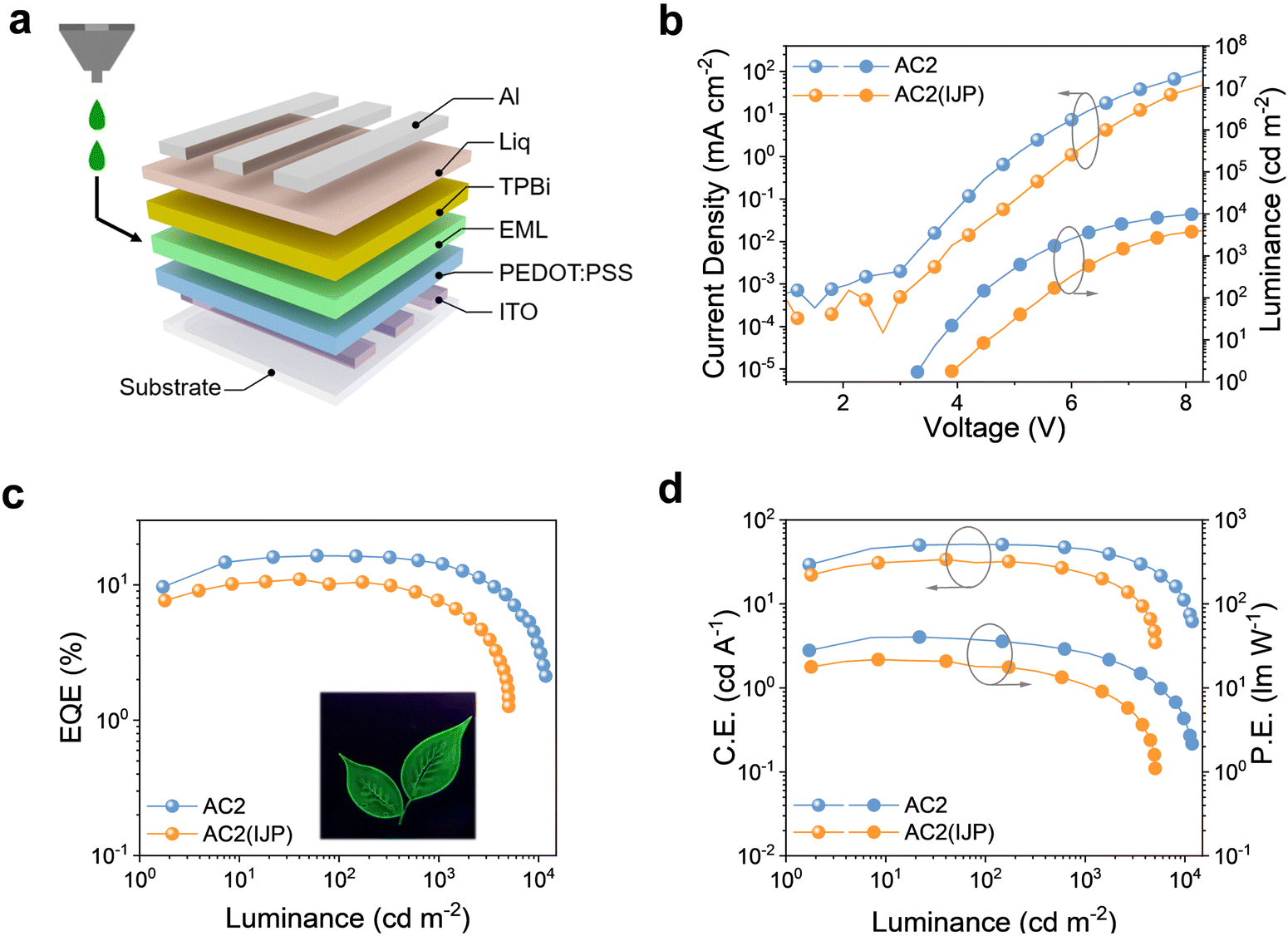 | ||
| Fig. 5 (a) Device structure and (b) J–V–L, (c) EQE, and (d) CE–L–PE of the inkjet-printed AC2 based OLED. Inset in (c): PL pattern of the inkjet-printed EML ink. | ||
| Device (host) | EQEa (%) | PEa (lm W−1) | CEa (cd A−1) | L max (cd m−1) | V T (V) | V D(V) @102, 103, 104 cd m−2 | CIEd (x,y) | |||||
|---|---|---|---|---|---|---|---|---|---|---|---|---|
| a Data at maximum and 1000 cd m−2 from left to right. b Maximum luminance. c Voltage at 1 cd m−2. d CIE: Commission Internationale de I’Eclairage at 1000 cd m−2. | ||||||||||||
| AC2 | 16.4 | 14.5 | 40.3 | 26.4 | 51.3 | 44.9 | 11820 | 3.2 | 4.4 | 5.4 | 8.2 | (0.29,0.55) |
| AC2(IJP) | 11.0 | 7.7 | 21.7 | 11.0 | 33.7 | 23.1 | 5041 | 3.5 | 4.5 | 5.5 | — | (0.28,0.54) |
Conclusions
Three alkyl group modified carbazole derivatives as new host materials for solution-processed TADF-OLEDs have been designed and synthesized, named AC1, AC2, and AC3. Compared with the classical CBP currently used in vacuum-deposited EMLs, all three host materials show improved thermostability and appropriate solubility, especially AC2 and AC3 with an asymmetric structure. They are highly suitable for solution-processed TADF-OLEDs. Through a detailed investigation, it was found that AC2 showed a more efficient energy transfer process. The AC2 based spin-coated TADF-OLED has a higher EQE/CE (16.4%/51.3 cd A−1) than the other two. Furthermore, the inkjet-printing method was successfully employed to fabricate a TADF-OLED with AC2 as the host for the EML which exhibited high EQE and CE (11.0% and 33.7 cd A−1), representing the highest value reported for inkjet-printed classical organic TADF-OLED devices.Conflicts of interest
The authors declare that they have no known competing financial interests or personal relationships that could have appeared to influence the work reported in this paper.Acknowledgements
This work was financially supported by China Postdoctoral Science Foundation (2020M681726), Natural Science Foundation of Jiangsu Province (BK20210125), and the Open-Foundation of Key Laboratory of Laser Device Technology, China North Industries Group Corporation Limited (KLLDT202105). The authors are grateful for the technical support for Nano-X from Suzhou Institute of Nano-Tech and Nano-Bionics, Chinese Academy of Sciences (SINANO).References
- C. W. Tang and S. A. VanSlyke, Organic electroluminescent diodes, Appl. Phys. Lett., 1987, 51(12), 913–915 CrossRef CAS.
- C.-J. Zheng, W.-M. Zhao, Z.-Q. Wang, D. Huang, J. Ye, X.-M. Ou, X.-H. Zhang, C.-S. Lee and S.-T. Lee, Highly efficient non-doped deep-blue organic light-emitting diodes based on anthracene derivatives, J. Mater. Chem., 2010, 20(8), 1560–1566 RSC.
- K. H. Kim, C. K. Moon, J. H. Lee, S. Y. Kim and J. J. Kim, Highly Efficient Organic Light-Emitting Diodes with Phosphorescent Emitters Having High Quantum Yield and Horizontal Orientation of Transition Dipole Moments, Adv. Mater., 2014, 26(23), 3844–3847 CrossRef CAS PubMed.
- M. A. Baldo, S. Lamansky, P. E. Burrows, M. E. Thompson and S. R. Forrest, Very high-efficiency green organic light-emitting devices based on electrophosphorescence, Appl. Phys. Lett., 1999, 75(1), 4–6 CrossRef CAS.
- M. A. Baldo, D. F. O'Brien, Y. You, A. Shoustikov, S. Sibley, M. E. Thompson and S. R. Forrest, Highly efficient phosphorescent emission from organic electroluminescent devices, Nature, 1998, 395(6698), 151–154 CrossRef CAS.
- Z. Y. Yang, Z. Mao, Z. L. Xie, Y. Zhang, S. W. Liu, J. Zhao, J. R. Xu, Z. G. Chi and M. P. Aldred, Recent advances in organic thermally activated delayed fluorescence materials, Chem. Soc. Rev., 2017, 46(3), 915–1016 RSC.
- A. Endo, K. Sato, K. Yoshimura, T. Kai, A. Kawada, H. Miyazaki and C. Adachi, Efficient up-conversion of triplet excitons into a singlet state and its application for organic light emitting diodes, Appl. Phys. Lett., 2011, 98(8), 083302 CrossRef.
- G. Hong, X. Gan, C. Leonhardt, Z. Zhang, J. Seibert, J. M. Busch and S. Brase, A Brief History of OLEDs-Emitter Development and Industry Milestones, Adv. Mater., 2021, 33(9), 2005630 CrossRef CAS PubMed.
- F. B. Dias, K. N. Bourdakos, V. Jankus, K. C. Moss, K. T. Kamtekar, V. Bhalla, J. Santos, M. R. Bryce and A. P. Monkman, Triplet Harvesting with 100% Efficiency by Way of Thermally Activated Delayed Fluorescence in Charge Transfer OLED Emitters, Adv. Mater., 2013, 25(27), 3707–3714 CrossRef CAS PubMed.
- R. Ishimatsu, S. Matsunami, T. Kasahara, J. Mizuno, T. Edura, C. Adachi, K. Nakano and T. Imato, Electrogenerated Chemiluminescence of Donor–Acceptor Molecules with Thermally Activated Delayed Fluorescence, Angew. Chem., Int. Ed., 2014, 53(27), 6993–6996 CrossRef CAS PubMed.
- T. A. Lin, T. Chatterjee, W. L. Tsai, W. K. Lee, M. J. Wu, M. Jiao, K. C. Pan, C. L. Yi, C. L. Chung, K. T. Wong and C. C. Wu, Sky-Blue Organic Light Emitting Diode with 37% External Quantum Efficiency Using Thermally Activated Delayed Fluorescence from Spiroacridine-Triazine Hybrid, Adv. Mater., 2016, 28(32), 6976–6983 CrossRef CAS PubMed.
- T.-L. Wu, M.-J. Huang, C.-C. Lin, P.-Y. Huang, T.-Y. Chou, R.-W. Chen-Cheng, H.-W. Lin, R.-S. Liu and C.-H. Cheng, Diboron compound-based organic light-emitting diodes with high efficiency and reduced efficiency roll-off, Nat. Photonics, 2018, 12(4), 235–240 CrossRef CAS.
- M. C. Gather, A. Kohnen and K. Meerholz, White Organic Light-Emitting Diodes, Adv. Mater., 2011, 23(2), 233–248 CrossRef CAS PubMed.
- S. R. Forrest, The path to ubiquitous and low-cost organic electronic appliances on plastic, Nature, 2004, 428(6986), 911–918 CrossRef CAS PubMed.
- F. Samaeifar and H. Aziz, The Root Causes of the Limited Electroluminescence Stability of Solution-Coated Versus Vacuum-Deposited Small-Molecule OLEDs: A Mini-Review, Front. Chem., 2022, 10, 857551 CrossRef CAS PubMed.
- F. So, B. Krummacher, M. K. Mathai, D. Poplavskyy, S. A. Choulis and V. E. Choong, Recent progress in solution processable organic light emitting devices, J. Appl. Phys., 2007, 102(9), 091101 CrossRef.
- K. W. Tsai, M. K. Hung, Y. H. Mao and S. A. Chen, Solution-Processed Thermally Activated Delayed Fluorescent OLED with High EQE as 31% Using High Triplet Energy Crosslinkable Hole Transport Materials, Adv. Funct. Mater., 2019, 29(15), 1901025 CrossRef.
- M. Singh, H. M. Haverinen, P. Dhagat and G. E. Jabbour, Inkjet Printing-Process and Its Applications, Adv. Mater., 2010, 22(6), 673–685 CrossRef CAS PubMed.
- B. J. de Gans, P. C. Duineveld and U. S. Schubert, Inkjet printing of polymers: State of the art and future developments, Adv. Mater., 2004, 16(3), 203–213 CrossRef CAS.
- L. Mu, M. J. He, C. B. Jiang, J. H. Wang, C. H. Mai, X. L. Huang, H. Zheng, J. Wang, X. H. Zhu and J. B. Peng, Inkjet printing a small-molecule binary emitting layer for organic light-emitting diodes, J. Mater. Chem. C, 2020, 8(20), 6906–6913 RSC.
- Y. J. Kang, R. Bail, C. W. Lee and B. D. Chin, Inkjet Printing of Mixed-Host Emitting Layer for Electrophosphorescent Organic Light-Emitting Diodes, ACS Appl. Mater. Interfaces, 2019, 11(24), 21784–21794 CrossRef CAS PubMed.
- M. Singh, H. M. Haverinen, P. Dhagat and G. E. Jabbour, Inkjet Printing—Process and Its Applications, Adv. Mater., 2010, 22(6), 673–685 CrossRef CAS PubMed.
- I. Verboven and W. Deferme, Printing of flexible light emitting devices: A review on different technologies and devices, printing technologies and state-of-the-art applications and future prospects, Prog. Mater. Sci., 2021, 118, 100760 CrossRef.
- Z. Yin, Y. Huang, N. Bu, X. Wang and Y. Xiong, Inkjet printing for flexible electronics: Materials, processes and equipments, Chin. Sci. Bull., 2010, 55(30), 3383–3407 CrossRef.
- R. S. Nobuyasu, Z. Ren, G. C. Griffiths, A. S. Batsanov, P. Data, S. Yan, A. P. Monkman, M. R. Bryce and F. B. Dias, Rational Design of TADF Polymers Using a Donor–Acceptor Monomer with Enhanced TADF Efficiency Induced by the Energy Alignment of Charge Transfer and Local Triplet Excited States, Adv. Opt. Mater., 2016, 4(4), 597–607 CrossRef CAS.
- X. L. Chen, R. M. Yu, Q. K. Zhang, L. J. Zhou, C. Y. Wu, Q. Zhang and C. Z. Lu, Rational Design of Strongly Blue-Emitting Cuprous Complexes with Thermally Activated Delayed Fluorescence and Application in Solution-Processed OLEDs, Chem. Mater., 2013, 25(19), 3910–3920 CrossRef CAS.
- Y. J. Cho, B. D. Chin, S. K. Jeon and J. Y. Lee, 20% External Quantum Efficiency in Solution-Processed Blue Thermally Activated Delayed Fluorescent Devices, Adv. Funct. Mater., 2015, 25(43), 6786–6792 CrossRef CAS.
- S. Gao, X. Chen, X. Ge, Z. Chen, J. Zhao and Z. Chi, Asymmetric Thermally Activated Delayed Fluorescence Materials Rendering High-performance OLEDs Through both Thermal Evaporation and Solution-processing, Chem. Res. Chin. Univ., 2022, 38, 1526–1531 CrossRef CAS.
- L. Chen, J. Lv, S. Wang, S. Shao and L. Wang, Dendritic Interfacial Exciplex Hosts for Solution-Processed TADF-OLEDs with Power Efficiency Approaching 100 lm W−1, Adv. Opt. Mater., 2021, 9(20), 2100752 CrossRef CAS.
- C. M. Cole, S. V. Kunz, P. E. Shaw, C. S. K. Ranasinghe, T. Baumann, J. P. Blinco, P. Sonar, C. Barner-Kowollik and S. D. Yambem, Inkjet-Printed Self-Hosted TADF Polymer Light-Emitting Diodes, Adv. Mater. Technol., 2022, 2200648 CrossRef CAS.
- C. Amruth, B. Luszczynska, M. Z. Szymanski, J. Ulanski, K. Albrecht and K. Yamamoto, Inkjet printing of thermally activated delayed fluorescence (TADF) dendrimer for OLEDs applications, Org. Electron., 2019, 74, 218–227 CrossRef.
- M. Wallesch, A. Verma, C. Flechon, H. Fluegge, D. M. Zink, S. M. Seifermann, J. M. Navarro, T. Vitova, J. Goettlicher, R. Steininger, L. Weinhardt, M. Zimmer, M. Gerhards, C. Heske, S. Braese, T. Baumann and D. Volz, Towards Printed Organic Light-Emitting Devices: A Solution-Stable, Highly Soluble Cu-I-NHetPHOS Complex for Inkjet Processing, Chem. – Eur. J., 2016, 22(46), 16400–16405 CrossRef CAS PubMed.
- A. Verma, D. M. Zink, C. Flechon, J. L. Carballo, H. Flugge, J. M. Navarro, T. Baumann and D. Volz, Efficient, inkjet-printed TADF-OLEDs with an ultra-soluble NHetPHOS complex, Appl. Phys. A: Mater. Sci. Process., 2016, 122(3), 191 CrossRef.
- L. Zhou, L. Yang, M. J. Yu, Y. Jiang, C. F. Liu, W. Y. Lai and W. Huang, Inkjet-Printed Small-Molecule Organic Light-Emitting Diodes: Halogen-Free Inks, Printing Optimization, and Large-Area Patterning, ACS Appl. Mater. Interfaces, 2017, 9(46), 40533–40540 CrossRef CAS PubMed.
- X. Ban, A. Zhu, T. Zhang, Z. Tong, W. Jiang and Y. Sun, Highly Efficient All-Solution-Processed Fluorescent Organic Light-Emitting Diodes Based on a Novel Self-Host Thermally Activated Delayed Fluorescence Emitter, ACS Appl. Mater. Interfaces, 2017, 9(26), 21900–21908 CrossRef CAS PubMed.
- S. V. Kunz, C. M. Cole, S. C. Gauci, F. Zaar, P. E. Shaw, C. S. K. Ranasinghe, T. Baumann, P. Sonar, S. D. Yambem, E. Blasco, C. Barner-Kowollik and J. P. Blinco, A simplified approach to thermally activated delayed fluorescence (TADF) bipolar host polymers, Polym. Chem., 2022, 13(29), 4241–4248 RSC.
- X. Ban, W. Jiang, K. Sun, B. Lin and Y. Sun, Self-Host Blue Dendrimer Comprised of Thermally Activated Delayed Fluorescence Core and Bipolar Dendrons for Efficient Solution-Processable Nondoped Electroluminescence, ACS Appl. Mater. Interfaces, 2017, 9(8), 7339–7346 CrossRef CAS PubMed.
- T. Chatterjee and K.-T. Wong, Perspective on Host Materials for Thermally Activated Delayed Fluorescence Organic Light Emitting Diodes, Adv. Opt. Mater., 2019, 7(1), 1800565 CrossRef.
- T. Northey, J. Stacey and T. J. Penfold, The role of solid state solvation on the charge transfer state of a thermally activated delayed fluorescence emitter, J. Mater. Chem. C, 2017, 5(42), 11001–11009 RSC.
- P. L. dos Santos, J. S. Ward, M. R. Bryce and A. P. Monkman, Using Guest–Host Interactions To Optimize the Efficiency of TADF OLEDs, J. Phys. Chem. Lett., 2016, 7(17), 3341–3346 CrossRef CAS PubMed.
- Z. Q. Gao, B. X. Mi, H. L. Tam, K. W. Cheah, C. H. Chen, M. S. Wong, S. T. Lee and C. S. Lee, High Efficiency and Small Roll-Off Electrophosphorescence from a New Iridium Complex with Well-Matched Energy Levels, Adv. Mater., 2008, 20(4), 774–778 CrossRef CAS.
- Y. H. Kim, C. Wolf, H. Cho, S. H. Jeong and T. W. Lee, Highly Efficient, Simplified, Solution-Processed Thermally Activated Delayed-Fluorescence Organic Light-Emitting Diodes, Adv. Mater., 2016, 28(4), 734–741 CrossRef CAS PubMed.
- M.-H. Tsai, Y.-H. Hong, C.-H. Chang, H.-C. Su, C.-C. Wu, A. Matoliukstyte, J. Simokaitiene, S. Grigalevicius, J. V. Grazulevicius and C.-P. Hsu, 3-(9-carbazolyl)carbazoles and 3,6-di(9-carbazolyl)carbazoles as effective host materials for efficient blue organic electrophosphorescence, Adv. Mater., 2007, 19(6), 862–866 CrossRef CAS.
- Y.-C. Chen, G.-S. Huang, C.-C. Hsiao and S.-A. Chen, High Triplet Energy Polymer as Host for Electrophosphorescence with High Efficiency, J. Am. Chem. Soc., 2006, 128(26), 8549–8558 CrossRef CAS PubMed.
- H. Uoyama, K. Goushi, K. Shizu, H. Nomura and C. Adachi, Highly efficient organic light-emitting diodes from delayed fluorescence, Nature, 2012, 492(7428), 234–238 CrossRef CAS PubMed.
- D. R. Lee, B. S. Kim, C. W. Lee, Y. Im, K. S. Yook, S. H. Hwang and J. Y. Lee, Above 30% External Quantum Efficiency in Green Delayed Fluorescent Organic Light-Emitting Diodes, ACS Appl. Mater. Interfaces, 2015, 7(18), 9625–9629 CrossRef CAS PubMed.
- Z. Du, Y. Liu, X. Xing, T. Lin, L. Liu, T. Chu, L. Wang, D. Zhang and Z. Cui, Inkjet printing multilayer OLEDs with high efficiency based on the blurred interface, J. Phys. D: Appl. Phys., 2020, 53(35), 355105 CrossRef CAS.
- Y.-X. Hu, T. Lin, X. Xia, W.-Y. Mu, Y.-L. Sun, W.-Z. He, C.-T. Wei, D.-Y. Zhang, X. Li and Z. Cui, Novel phosphorescent iridium(iii) emitters for both vacuum-deposition and inkjet-printing of OLEDs with exceptionally high efficiency, J. Mater. Chem. C, 2019, 7(14), 4178–4184 RSC.
- T. Lin, X. Sun, Y. X. Hu, W. Y. Mu, Y. L. Sun, D. Y. Zhang, Z. S. Su, B. Chu and Z. Cui, Blended host ink for solution processing high performance phosphorescent OLEDs, Sci. Rep., 2019, 9, 6849 CrossRef PubMed.
- Y. Wang, J. H. Yun, L. Wang and J. Y. Lee, High Triplet Energy Hosts for Blue Organic Light-Emitting Diodes, Adv. Funct. Mater., 2021, 31(12), 2008332 CrossRef CAS.
- C. Poriel and J. Rault-Berthelot, Designing Host Materials for the Emissive Layer of Single-Layer Phosphorescent Organic Light-Emitting Diodes: Toward Simplified Organic Devices, Adv. Funct. Mater., 2021, 31(24), 2010547 CrossRef CAS.
- Y. Tao, C. Yang and J. Qin, Organic host materials for phosphorescent organic light-emitting diodes, Chem. Soc. Rev., 2011, 40(5), 2943–2970 RSC.
- S. Manzetti and T. Lu, The geometry and electronic structure of Aristolochic acid: possible implications for a frozen resonance, J. Phys. Org. Chem., 2013, 26(6), 473–483 CrossRef CAS.
- B. Derby, Inkjet Printing of Functional and Structural Materials: Fluid Property Requirements, Feature Stability, and Resolution, Annu. Rev. Mater. Res., 2010, 40(1), 395–414 CrossRef CAS.
- G. D. Martin, S. D. Hoath and I. M. Hutchings, Inkjet printing - the physics of manipulating liquid jets and drops, J. Phys.: Conf. Ser., 2008, 105(1), 012001 CrossRef.
Footnote |
| † Electronic supplementary information (ESI) available. See DOI: https://doi.org/10.1039/d2tc05322e |
| This journal is © The Royal Society of Chemistry 2023 |