
Chemical vapor etching of silicon wafer for the synthesis of highly dense and aligned sub-5 nm silicon nanowire arrays†
 ‡*a
Yung Joon
Jung
*ab
‡*a
Yung Joon
Jung
*ab
Abstract
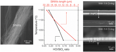
Silicon nanowires (SiNWs) have attracted great interest for applications in high-performance miniaturized devices and energy-harvesting and -storage systems. Vapor–liquid–solid growth and metal-assisted chemical etching methods are the most commonly used approaches for synthesizing silicon nanowires. However, using these catalyst-assisted methods, producing a large quantity of silicon nanowires with diameters less than 10 nm is elusive, and removal of the catalysts is a challenge for their practical applications. Recently, we reported the synthesis of highly dense and vertically aligned sub-5 nm silicon nanowires with a high aspect ratio of over 10 000 via the catalyst-free chemical vapor etching of silicon. In this paper, we systematically investigated the effect of key chemical vapor etching parameters that govern the morphology of silicon nanowires. We achieved highly aligned nanowire arrays with sub-5 nm diameters and lengths of up to 52.1 μm by controlling the oxidant gas concentration, the reaction temperature, and the hydrogen concentration. These results demonstrate that the ppm level of oxidant gases is crucial for the steady-state etching of silicon into nanowires via passivating their surface with a silicon suboxide layer. Furthermore, thermodynamic analysis combined with the experimental results suggests that the anisotropic etching of silicon is also facilitated by increasing the reaction temperature and hydrogen concentration, due to the increased ratio between the two primary etchants (HCl/SiCl4), suggesting an optimum range of the etchant ratio (i.e., 0.131–0.216) for nanowire formation. Our results can help us to understand the chemical vapor Si etching process and guide the scalable synthesis of ultra-narrow silicon nanowires for future scientific research and practical applications.
 Please wait while we load your content...

