
 Open Access Article
 This Open Access Article is licensed under a Creative Commons Attribution-Non Commercial 3.0 Unported Licence
Te and Ge solid-state reaction: comparison between the 2D and 3D growth of α-GeTe
Guillaume
Roland
ab,
Alain
Portavoce
 *a,
Maxime
Bertoglio
a,
Marion
Descoins
a,
Jacopo
Remondina
a,
Frédéric
Lorut
b and
Magali
Putero
*a
*a,
Maxime
Bertoglio
a,
Marion
Descoins
a,
Jacopo
Remondina
a,
Frédéric
Lorut
b and
Magali
Putero
*a
aAix Marseille Univ., CNRS, IM2NP UMR7334, Campus Scientifique de St Jérôme, 13397, Marseille cedex 20, France. E-mail: magali.putero@univ-amu.fr; alain.portavoce@im2np.fr
bSTMicroelectronics, 850 rue Jean Monnet, 38920, Crolles, France
First published on 6th February 2023
Abstract
In this work, solid-state α-GeTe growth is studied during the reactive diffusion of a polycrystalline thin film of hexagonal Te deposited on an amorphous Ge thin film (Te-on-Ge) using in situ X-ray diffraction, in situ transmission electron microscopy, and atom probe tomography. After deposition, an amorphous intermixing layer is observed between the Te and Ge layers. α-GeTe is found to form a 2D layer between the deposited Ge and Te layers during growth, with a thickness increasing linearly with time as predicted by the linear-parabolic model for interfacial reaction limited growth. The activation energy of nucleation and interfacial reactions was determined from different isothermal annealing. The obtained results are compared to the observations previously reported during α-GeTe 3D growth in a sample made of an amorphous Ge layer deposited on a polycrystalline Te layer (Ge-on-Te) in the same magnetron sputtering system under the same conditions.
1. Introduction
Phase change materials (PCMs) are a class of materials, mostly composed of chalcogenides glasses,1,2 which attract a lot of attention for their surprising phase change properties. Indeed, PCMs can reversibly and quickly change between a high-resistivity amorphous (and in general low-reflectivity) state and a low-resistivity crystalline (and in general high-reflectivity) state through thermal annealing.1–3 This property has been exploited for nonvolatile optical memories such as CDs, DVDs and Blu-ray discs, using the large reflectivity difference between the two states.1–4 PCM's properties are also exploited for Phase Change Random Access Memory (PCRAM) applications. PCRAM is a new kind of non-volatile memory. In this memory, the bit of information is given by the state of the PCM: “0” if the PCM is in its highly resistive amorphous state, “1” if the PCM is in its low resistive crystalline state. The two most studied and prototypical materials for PCRAM applications are the compounds GeTe and Ge2Sb2Te5 (GST225).1,2,4 However, the low crystallization temperature of GST225 (∼150–170 °C2) can be a limiting factor for high reliability applications,5,6 such as automotive applications. In contrast, GeTe has a higher crystallization temperature than GST225 (∼180–230 °C depending on oxidation7) and exhibits ultra-fast switching.8 GeTe is also studied for thermoelectric9–11 and RF switch applications.12–14 For all these applications, it is important to understand the GeTe growth mechanisms. Several studies have shown and studied the possibility to grow high quality epitaxial GeTe using either molecular beam epitaxy or pulsed laser deposition techniques, enabling to grow ultrathin (down to 1 nm) epilayers for ferroelectricity applications15,16 or strain engineering17 for example. However, most studies that seek to investigate GeTe focus on the crystallization of an amorphous homogeneous stoichiometric, or near-stoichiometric, thin film. These studies use a plethora of different techniques: differential scanning calorimetry (DSC),18,19in situ resistivity measurements,20–22in situ reflectivity measurement,19,23,24 transmission electron microscopy (TEM) observations,7,24–27 X-ray diffraction (XRD),18,20,28,29 X-ray photoelectron spectroscopy (XPS),26,30,31etc. Even though these studies provide key insights into the crystallization mechanisms, they do not give information about self-diffusion and interfacial reaction kinetics as reactive diffusion (RD) studies between two films in contact. RD is often used in the microelectronic industry in order to form silicide ohmic contacts on the source, gate and drain of metal-oxide-semiconductor (MOS) transistors through the self-aligned-silicide (salicide) process.32–34 Since RD depends on self-diffusion and interfacial reactions, it is used to obtain information on the self-diffusion and interfacial reaction kinetics, which are of prime importance for process simulations and crystallization understanding. When a metal is deposited on a Ge or Si substrate, it is usual to observe a 3–5 nm-thick, amorphous or crystalline, intermixing layer.35–38 For germanides, the growth usually follows a parabolic law versus time.39–41 This means that the growth is limited by atomic diffusion according to the linear-parabolic model.42In this work, GeTe growth kinetics is studied during the RD of a 90 nm-thick polycrystalline Te layer deposited by magnetron sputtering on a 60 nm-thick amorphous Ge layer (Te-on-Ge) using in situ XRD measurements, in situ TEM observations, as well as ex situ atom probe tomography (APT). We show that contrary to the reverse stack Ge-on-Te,43 the growth of α-GeTe during RD of the Te-on-Ge bilayer follows a 2D growth described by the linear-parabolic growth model, with higher crystallization temperature and nucleation activation energy compared to that found during the 3D growth observed in the Ge-on-Te bilayer.43 The activation energy of the interfacial reaction is also determined and compared to the α-GeTe 3D growth activation energy.43
2. Experimental details
2.1. Film deposition
The sample was elaborated in a commercial magnetron sputtering system (base pressure of 10−8 mbar). A 99.9999% pure Ar gas flow under a work pressure of 3.6 × 10⁻³ mbar was used in order to sputter a 99.99% pure Te-target in the RF mode and a 99.999% pure Ge-target in the DC mode, using same sputtering powers and deposition time as in the previous study reported in ref. 43. All the deposition have been made on the native oxide of the Si(001) substrate at room temperature (RT) and both fluxes were calibrated separately by measuring the thickness of the sputtered films using X-ray reflectivity. The thin SiO2 layer (∼2 nm) was kept in order to prevent the diffusion of Si in the deposited layers.The sample was destined to the study of solid-state Te-on-Ge reactive diffusion (RD). Therefore, a 90 nm-thick Te layer was deposited on top of a 60 nm-thick Ge layer. After the entire bilayer has reacted, it is expected to have a GeTe layer with an extra 10 nm-thick Te layer on the surface. This extra-layer was added in order to limit oxidation effects. After deposition (Fig. 1), the Ge layer is amorphous (a-Ge), whereas the Te layer is polycrystalline (poly-Te).
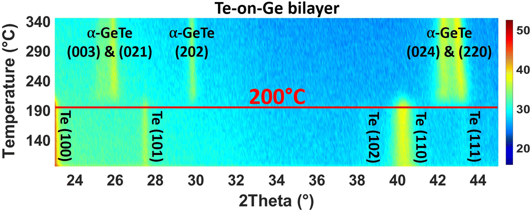 | ||
| Fig. 1 XRD patterns (λ = 0.154 nm) as a function of temperature acquired during in situ isochronal annealing of ∼ 0.9 K min−1 for Te-on-Ge bilayer. The color plot panel is in counts per s. | ||
2.2. In situ X-ray Diffraction experiments
After deposition, the samples (6 × 6 cm2) were cut into several pieces. 1.5 × 1.5 cm2 specimens were used to perform in situ XRD measurements. All the XRD measurements were achieved in the Bragg–Brentano geometry (θ − 2θ) in a Panalytical Empyrean diffractometer equipped with a PIXcel detector designed for high speed data collection, using a Cu Kα source (λ = 0.154 nm). The specimens were annealed following a heating ramp (isochronal annealing) or at constant temperature (isothermal annealing) in situ in the XRD setup under a vacuum of ∼10−5 mbar. A temperature ramp identical to that of our previous work was used:43 heating ramp was performed between 100 °C and 350 °C following a temperature ramp of 10 °C min−1 steps every 5 °C, separated by 4.5 minute-long XRD scans at a constant temperature, thus corresponding to an average heating ramp of ∼0.9 °C min−1. In addition to the ramp annealing, four isothermal annealing between 160 °C and 205 °C were performed on the sample.2.3. In situ transmission electron microscopy experiments
In situ TEM observations gave complementary information on the growth of the GeTe phase during Te-on-Ge RD. A TEM lamella was prepared using the in situ lift out technique in a FIB-SEM system, Helios450TM from ThermoFisher, and mounted onto a Molybdenum grid. The final thinning of the lamella was done using an 8 kV acceleration voltage, in order to limit possible Ga FIB induced amorphization. Once prepared, the grid was mounted onto a sample heating holder from Gatan and then loaded into a Technai F20 TEM, from ThermoFisher, operating at a 200 kV accelerating voltage in the TEM bright field mode. The in situ TEM annealing started at RT up to 350 °C following several isothermal steps. During each isothermal step, one image was taken every minute. The total annealing time was about 1 hour and 40 minutes.2.4. Atom probe tomography experiments
APT sample preparation was achieved using an FEI Helios dual-beam focused ion beam (FIB) equipped with a micromanipulator and a gas injection system for Pt deposition. Prior to FIB preparation, the sample’ surface was capped by a 100 nm-thick Ni protection layer deposited by sputtering. In the FIB set up, an additional 100 nm thick Pt protection layer was added on the region of interest, in order to prevent Ga contamination during the trench milling process. The region of interest was prepared in the cross-section geometry, retrieved using a micromanipulator, and placed on APT support. The specimen was shaped as a sharp tip by focused Ga+ ion beam milling and the top of the specimen was cleaned by low energy (2 keV) ion beam milling, as a final step. The samples were analyzed in a LEAP 3000X HR instrument. The specimens’ temperature was set to 50 K and the voltage pulse to 20% of the constant voltage.3. Results and discussion
3.1. GeTe growth during isochronal annealing
Fig. 1 is a series of XRD patterns recorded during the ramp annealing of the sample as a function of temperature. After deposition, 5 peaks are detected at 2θ = 23.04°, 27.497°, 38.26°, 40.369° and 43.485°. They, respectively, correspond to the (100), (101), (102), (110), and (111) Bragg reflections of the hexagonal Te phase, showing that the as-deposited Te layer is polycrystalline. No diffraction peak corresponding to the Ge phase is observed, meaning that the as-deposited Ge layer is amorphous. At T = 200 °C, five peaks are simultaneously detected. These peaks are found at 2θ = 25.359°, 26.014°, 29.863°, 42.351° and 43.138° and they, respectively, correspond to the (003), (021), (202), (024), and (220) Bragg reflections of the rhombohedral α-GeTe phase. The hex-Te (100) and (110) Bragg reflections and the α-GeTe (220) peaks are the most intense peaks for the Te and GeTe phases.Fig. 2 presents the variation of the normalized integrated XRD intensities and the variation of the average GeTe grain size L along the normal of the sample surface versus temperature. The average grain size is deduced from the full width at half maximum (FWHM) of the α-GeTe (220) peak, using the Scherrer formula44 and neglecting micro-strain contribution. The XRD integrated intensity is proportional to the corresponding diffracting volume. For the hex-Te phase, only the Te (110) is presented since it is the most intense peak correctly detected in Fig. 1. For the GeTe phase, only the most intense α-GeTe (220) peak is shown, however, we have to note that the α-GeTe (202) peak integrated intensity follows the same trend and will be shown for isothermal annealing. The α-GeTe phase appears at T ∼ 200 °C (i.e. nucleation temperature) and grows until T ∼ 220 °C. The nucleation temperature Tn ∼ 200 °C is higher than that reported for the reverse bilayer Ge-on-Te with Tn = 175 °C.43 Above 220 °C, the crystallized fraction of GeTe remains constant until the end of the temperature ramp. The appearance and the increase of the normalized integrated intensity of the α-GeTe (220) peak is concomitant with the decrease of the normalized integrated intensity of the hex-Te (110) peak.
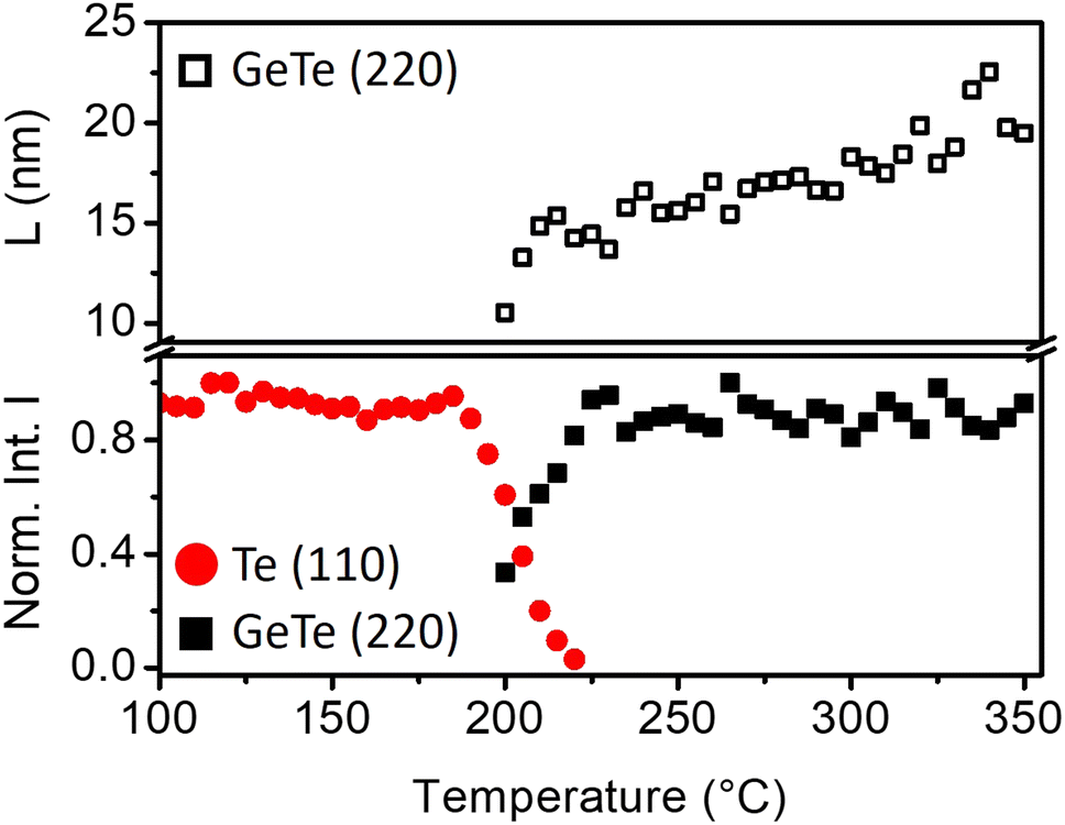 | ||
| Fig. 2 Normalized integrated intensities of diffraction peaks and average grain size (L) during in situ XRD isochronal annealing of ∼ 0.9 °C min−1 of Te-on-Ge bilayer: hex-Te (110) (red circles) and α-GeTe (220) (black squares). | ||
This is caused by the consumption of the hex-Te phase by the α-GeTe growing phase, which is a typical behavior for compound growth by RD.45 The GeTe growth is not perfectly correlated with the decrease of Te in Fig. 2. Indeed, the hex-Te is consumed from 190 °C, but the α-GeTe phase is only detected from 200 °C. This could be caused by the XRD detection limit, meaning that the diffracting volume of the α-GeTe phase is too small to be detected by XRD between 190–200 °C. Another hypothesis is that the GeTe phase grows in an amorphous state between 190 °C and 200 °C, the nucleation of the crystalline α-GeTe starting at 200 °C. This amorphous growth as already been observed for several silicides.37,38,46 Compared to the previous work on the reverse bilayer (Ge-on-Te, see43), the α-GeTe growth rate seems to be different in these two samples, especially at the early growth stages, even if both should depend on atomic transport kinetics.42,47
At the beginning of the growth, the average α-GeTe (220) grain size is L ∼ 10 nm. A first increase occurs rapidly up to L ∼ 15 nm between 200 °C and 220 °C, then the grain size slowly increases further to reach L ∼ 20 nm at the end of the annealing. The average α-GeTe grain size at the beginning of the growth is slightly smaller than that reported for the reverse stack (Ge-on-Te bilayer43). Besides, at the end of the annealing, the grain size (∼ 20 nm) is still smaller for the present sample Te-on-Ge compared to the Ge-on-Te bilayer (∼ 35 nm, see ref. 43). The texture is also different for both Te and GeTe phases. Indeed, in the present work (Te-on-Ge), the most intense peaks for the hex-Te phase correspond to the (100) and (110) Bragg reflections, and to the GeTe (220) peak for the α-GeTe phase. For the reverse stack (Ge-on-Te bilayer), almost the same peaks are observed, but the principal difference stands from their relative intensities: the most intense peaks are the Te (101) and the GeTe (202) Bragg reflections for, respectively, hex-Te and α-GeTe. The deposition power and time were kept the same for both samples, meaning that the only difference between the samples is the order of deposition. Indeed, the Te layer was deposited on the Si (001) substrate with a native oxide layer43 for Ge-on-Te instead of on the a-Ge layer for Te-on-Ge. This is probably the reason for the hex-Te texture difference in the two samples. Usually, germanides and silicides RD studies are performed on the system metal deposited on the semiconductor substrate. In this case, the substrate texture has been shown to have an impact on the nucleation temperature of the formed phase.48 Therefore, it would not be surprising that the hex-Te texture impacts Tn and the texture of the phase α-GeTe.
3.2. GeTe growth during isothermal annealing
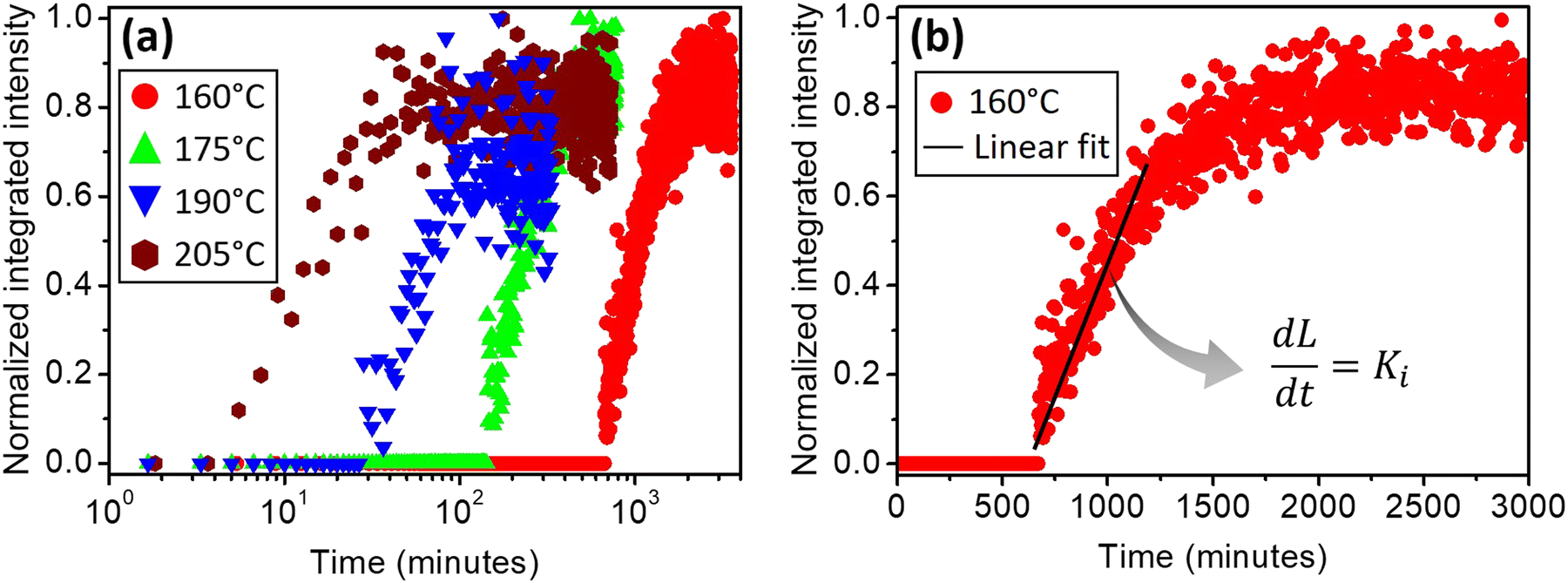
Several in situ isothermal XRD annealing were performed between T = 160 °C and 205 °C. Fig. 3(a) presents the variation of the α-GeTe(202) XRD normalized integrated intensity versus time for four different temperatures. The signal is proportional to the crystallized α-GeTe volume (i.e; crystallized fraction). The GeTe growth seems to follow the 2D linear-parabolic law,42 in contrast to the GeTe growth from the Ge-on-Te bilayer that surprisingly followed the JMAK model with a 3D growth.43 For each isothermal temperature, the beginning of the growth could be fitted with a linear law versus time (shown in Fig. 3(b) for the annealing at the lowest temperature), indicating that the growth is limited by the reaction. This result is surprising for germanides, for which RD is usually governed by self-diffusion, exhibiting a parabolic growth law versus time. The slope of the linear fit allows determining the interface reaction rate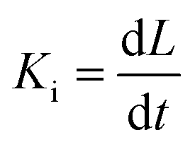 for each temperature, with L the thickness of the growing α-GeTe layer, that is proportional to the normalized integrated intensity assuming a 2D linear growth. The results are summarized in Table 1. The interface reaction rate can be expressed as follows:
where kB is the Boltzmann constant and T is the temperature, while K0 and Ei are the pre-exponential factor and the activation energy of the interface reaction, respectively. Fig. 4(a) shows the variation of ln(Ki) as a function of
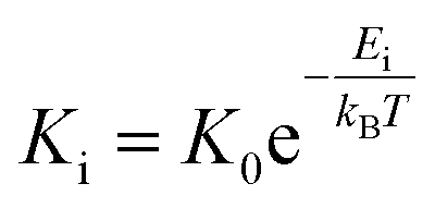
 . The activation energy of interfacial reaction was found to be Ei = 1.3 ± 0.1 eV. This energy is of the same order as the growth activation energy found for the reverse bilayer (1.2 eV for Ge-on-Te RD)43 but higher than that of the usual interface reaction of silicides or germanides (0.8 eV for Ni2Si,49 0.9 eV for Ni5Ge345).
 | ||
| Fig. 3 Normalized integrated intensity f(t) of the α-GeTe(202) diffraction peak versus time recorded during in situ XRD isothermal annealing of the Te-onGe bilayer at various temperatures: (a) versus time in log scale for temperatures between 160 °C and 205 °C; (b) versus time in linear scale at 160 °C, the solid line corresponds to a linear fit of the beginning of the growth. | ||
| Temperature (°C) | K i (a.u.) |
|---|---|
| 160 | 1.59 × 10⁻⁵ |
| 175 | 6.40 × 10⁻⁵ |
| 190 | 1.47 × 10⁻⁴ |
| 205 | 4.96 × 10⁻⁴ |
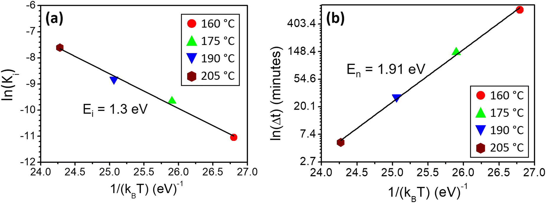 | ||
| Fig. 4 (a) Variations of ln(Ki), with Ki the interface reaction rate, as a function of the inverse of temperature for α-GeTe growth during the Te-on-Ge bilayer reactive diffusion; (b) variations of the nucleation time ln(Δt) as a function of the inverse of temperature for GeTe nucleation during Te-on-Ge bilayer reactive diffusion. | ||
The data presented in Fig. 3 can also be used to measure α-GeTe nucleation time Δt, which is defined as the time needed to detect for the first time the diffraction signal during isothermal annealing. Fig. 4(b) presents the variation of Δt versus 1/kBT using a logarithmic scale and allowed a nucleation activation energy to be determined, using the following equation:
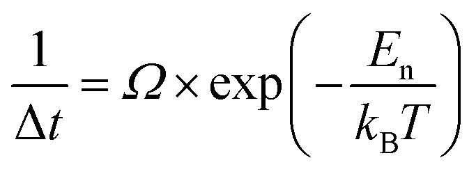
The nucleation activation energy of the α-GeTe phase was found to be En = 1.91 ± 0.15 eV. This value is higher than that found for the reverse bilayer (En = 1.25 eV),43 which reflects the difference between their nucleation temperatures. Besides, both the activation energies for nucleation and interfacial reaction are lower than the ones usually found for GeTe amorphous layer crystallization.50–52 This is probably due to the fact that in this study, GeTe crystallization occurs through reactive diffusion at the Te-on-Ge interface, whereas it occurs homogeneously in the GeTe layer volume when GeTe crystallization is studied from an initially amorphous GeTe layer.
In situ TEM observations were performed in order to better understand α-GeTe growth mechanisms. Four TEM images recorded during in situ observations are presented in Fig. 5. The annealing temperature goes from RT to 240 °C. After deposition (Fig. 5(a)), the sample is composed of a 91 nm-thick polycrystalline Te layer and a 49 nm-thick Ge amorphous layer. A 4 nm-thick amorphous intermixing layer can be observed at the Te/Ge interface. It is usual to observe a 3 to 5 nm-thick amorphous or crystalline intermixing layer between a metal and the Si or Ge substrate after sputtering.35–38 This layer acts usually as the initial stage of the 2D growth of silicides or germanides.47 During annealing (Fig. 5(b) to (d)), the intermixing layer grows as a continuous 2D layer, while voids form at the top of the Te layer. The void formation might be due to the Kirkendall effect, meaning that Te could be the main diffusive species, or to Te desorption in the annealing conditions due to its high volatility under vacuum. One should note that even if the top Te layer is oxidized, it does not affect the GeTe growth that starts at the Te/Ge interface. In Fig. 5(b) recorded at 180 °C, the intermixing layer has grown compared to Fig. 5(a) (from ∼4 nm to ∼8 nm), but is still amorphous (Fig. 5(b)). From Fig. 5(c) (195 °C), the intermixing layer appears partially crystalline. These TEM observations show that the intermixing layer firstly grows amorphous (from ∼4 to ∼8 nm) and then nucleation takes place, in agreement with the XRD results obtained during isochronal annealing. The crystallized part of the intermixing layer is believed to be α-GeTe, as shown by XRD (Fig. 1). These observations are also in agreement with the in situ XRD isothermal annealing: α-GeTe growth follows a 2D growth according to the linear-parabolic growth model, with a linear growth during the first stages, limited by the reaction.
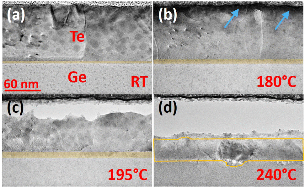 | ||
| Fig. 5 Cross-section TEM images acquired during in situ heating of a Te-on-Ge bilayer from RT to 240 °C: (a) RT; (b) 180 °C, the blue arrows indicate the void formation; (c) 195 °C; (d) 240 °C. The added color highlights the new phase. | ||
The chemical composition of the amorphous intermixing layer was measured by APT after deposition. Fig. 6 shows a high resolution TEM image of the amorphous GeTe intermixing layer with its APT proximity histogram (proxigram). The proxigram shows the average variation in the concentration of Ge (red line) and Te (green line) atoms from the perpendicular direction at each point of the isosurface used to define the outline of the interface. The concentration profile shows the composition of the intermixing layer after deposition. The Ge (Te) concentration gradient varies linearly from 100 at% (0 at%) to 0 at% (100 at%) in a ∼4.5 nm region corresponding to the intermixing layer. The measured intermixing layer's thickness is in good agreement with TEM observations (Fig. 5a).
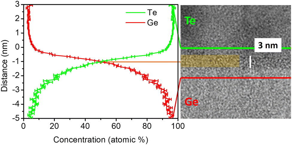 | ||
| Fig. 6 High resolution TEM image of the GeTe amorphous intermixing layer, highlighted by the added color; the vertical white bar corresponds to 3 nm. The chemical composition of the intermixing layer is determined by a proximity histogram (proxigram) measured from a 85 at% Te isoconcentration surface. | ||
3.3. Comparison between 2D and 3D α-GeTe growth
Solid state reaction is significantly different in our two samples Ge-on-Te43 and Te-on-Ge (this work) despite same sputtering conditions. Indeed, α-GeTe formation in the Ge-on-Te sample was shown to be supported by both nucleation in Te grain boundaries (GBs) and at the a-Ge/poly-Te interface, and the growth was shown to be following the JMAK model due to a simultaneous 3D growth in Te GBs and in the a-Ge layer, supported by interfacial diffusion and bulk GB self-diffusion. In contrast, α-GeTe formation in the Te-on-Ge sample is supported by nucleation in a concentration gradient53 in a 2D amorphous layer located between a-Ge and poly-Te, and α-GeTe increases linearly versus time as a 2D layer in agreement with linear-parabolic models, meaning that the growth is limited by interfacial reaction instead of self-diffusion.The difference of α-GeTe nucleation mechanisms between the two systems Te-on-Ge and Ge-on-Te leads to a higher Tn = 200 °C (ramp annealing) and En = 1.91 eV (isothermal annealing) for Te-on-Ge reaction compared to Ge-on-Te reaction displaying Tn = 175 °C and En = 1.25 eV.43 However, α-GeTe activation energy of growth is found to be similar in the two samples, with Ei = 1.3 eV in the Te-on-Ge sample and Eg = 1.2 eV in the Ge-on-Te sample, despite a 2D growth in the Te-on-Ge sample and a 3D growth in the Ge-on-Te sample. This observation means that the reaction Ge + Te → α-GeTe is almost independent of atomic diffusion mechanisms during 2D (GB self-diffusion) and 3D (interface and GB diffusion) growth, which agrees with the observation of a linear 2D growth in the Te-on-Ge sample. Indeed, α-GeTe linear growth versus time suggests that Ge and Te self-diffusion in α-GeTe GBs is unusually fast compared to reaction, contrasting with the growth of other germanides reported to date.39–41 RD studies are mostly performed for microelectronic process improvement, and thus, more data are actually available about silicide RD than about germanide RD. Typically, Ei ≤ 1 eV (0.8 eV for Ni2Si49 and 0.9 eV for Ni5Ge3,45 for example) and the growth rate is limited by self-diffusion (parabolic growth) with an activation energy 1 < Eg < 2 eV (1.5 eV for Ni2Si,49 for example) for silicide RD. One can note that indeed Ei in the case of Te-Ge RD is about 45% higher than expected, exhibiting a value close to that of silicide effective atomic self-diffusion, confirming the unusual specificity of the Ge-Te binary system characterized by a limiting slow interfacial reaction and fast self-diffusion.
The growth mode difference between the two systems Te-on-Ge (2D) and Ge-on-Te (3D) is probably linked to the presence (case of Te-on-Ge) or not (case of Ge-on-Te) of the intermixing layer between a-Ge and poly-Te. Most silicide and germanide RD studies concern only the case of the metal deposited onto Si or Ge, and the presence after deposition of an intermixing layer between the metal and the semiconductor is generally reported. Therefore, our observations are difficult to compare to most of the bibliography. Nevertheless, Perrin-Toinin et al.35 observed after sputtering the presence of an intermixing layer in both cases, Pd deposited on Ge and Ge deposited on Pd, and observed a 2D self-diffusion limited (parabolic) growth of Pd2Ge in the two cases. Using APT measurements, they showed that the thickness (∼5 nm) and the composition (close to Pd2Ge stoichiometry) of the intermixing layer were about the same for the two systems Pd/Ge and Ge/Pd. These results suggest that the 3D regime observed for Ge-on-Te is due to the absence of the intermixing layer in this case. In addition to a growth rate obeying the JMAK model, the signature of 3D growth in the Ge-on-Te sample is also observed on the average grain size. L is found to be about 75% larger in the Ge-on-Te sample (L ∼ 35 nm) compared to in the Te-on-Ge sample (L ∼ 20 nm) at the end of the growth, 3D growth promoting longer grains in the direction perpendicular to the sample surface.
Conclusion
Te-Ge reactive diffusion has been studied by in situ XRD, in situ TEM, and APT in a sample made of a poly-Te layer deposited on an a-Ge layer and compared to the reverse case of an a-Ge layer deposited on a poly-Te layer in the same magnetron sputtering system under same conditions. α-GeTe grows between poly-Te and a-Ge in the Te-on-Ge sample as a 2D layer with a linear growth rate versus time in agreement with the linear-parabolic model, contrasting with the 3D growth obeying the JMAK model previously reported in the Ge-on-Te sample. The growth mode difference appears to be related to the absence of an intermixing layer between a-Ge and poly-Te in the as-deposited Ge-on-Te sample. The nucleation temperature and the nucleation activation energy are found to be higher for the 2D growth in the Te-on-Ge sample. However, with the growth activation energy during 2D linear growth in the Te-on-Ge sample and during 3D JMAK growth in the Ge-on-Te sample being similar, the overall observations coherently suggest that α-GeTe growth is limited by an unusually slow solid-state reaction combined with unusually fast GB (or interfacial) self-diffusion, compared to available literature data on silicides and germanides.Author contributions
Guillaume Roland: investigation, validation, formal analysis, data curation, visualization, writing – original draft. Alain Portavoce: conceptualization, methodology, review & editing, Writing – review & editing, supervision, project administration, funding acquisition. Maxime Bertoglio: investigation, methodology. Marion Descoins: methodology, formal analysis. Jacopo Remondina: investigation, validation, formal analysis. Frédéric Lorut: investigation, methodology, project administration. Magali Putero: conceptualization, methodology, writing – review & editing, supervision, project administration, funding acquisition.Conflicts of interest
There are no conflicts to declare.Acknowledgements
This project was supported by the French National Association of Research and Technology (ANRT Project 2020/0907).References
- S. Raoux, G. W. Burr, M. J. Breitwisch, C. T. Rettner, Y. C. Chen, R. M. Shelby, M. Salinga, D. Krebs, S. H. Chen, H. L. Lung and C. H. Lam, IBM J. Res. Dev., 2008, 52, 465–479 CAS.
- P. Noé, C. Vallée, F. Hippert, F. Fillot and J.-Y. Raty, Semicond. Sci. Technol., 2018, 33, 13002 CrossRef.
- M. Wuttig and N. Yamada, Nat. Mater., 2007, 6, 824–832 CrossRef CAS PubMed.
- N. Yamada, Phys. Status Solidi B, 2012, 249, 1837–1842 CrossRef CAS.
- S. Privitera, E. Rimini and R. Zonca, Appl. Phys. Lett., 2004, 85, 3044–3046 CrossRef CAS.
- E. Gomiero, G. Samanni, J. Jasse, C. Jahan, O. Weber, R. Berthelon, R. Ranica, L. Favennec, V. Caubet, D. Ristoiu, J. P. Reynard, L. Clement, P. Zuliani, R. Annunziata and F. Arnaud, IEEE J. Electron Devices Soc., 2019, 7, 517–521 CAS.
- R. Berthier, N. Bernier, D. Cooper, C. Sabbione, F. Hippert and P. Noé, J. Appl. Phys., 2017, 122, 115304 CrossRef.
- G. Bruns, P. Merkelbach, C. Schlockermann, M. Salinga, M. Wuttig, T. D. Happ, J. B. Philipp and M. Kund, Appl. Phys. Lett., 2009, 95, 043108 CrossRef.
- A. Suwardi, S. H. Lim, Y. Zheng, X. Wang, S. W. Chien, X. Y. Tan, Q. Zhu, L. M. N. Wong, J. Cao, W. Wang, Q. Yan, C. K. I. Tan and J. Xu, J. Mater. Chem. C, 2020, 8, 16940–16948 RSC.
- J. Li, Z. Chen, X. Zhang, Y. Sun, J. Yang and Y. Pei, NPG Asia Mater., 2017, 9, e353–e358 CrossRef CAS.
- S. Perumal, S. Roychowdhury and K. Biswas, J. Mater. Chem. C, 2016, 4, 7520–7536 RSC.
- N. El-Hinnawy, P. Borodulin, B. Wagner, M. R. King, J. S. Mason, E. B. Jones, S. McLaughlin, V. Veliadis, M. Snook, M. E. Sherwin, R. S. Howell, R. M. Young and M. J. Lee, IEEE Electron Device Lett., 2013, 34, 1313–1315 CAS.
- T. Singh and R. R. Mansour, 2018 IEEE MTT-S Int. Microw. Work. Ser. Adv. Mater. Process. RF THz Appl. IMWS-AMP 2018, 2018, 1–3.
- A. Ghalem, A. Hariri, C. Guines, D. Passerieux, L. Huitema, P. Blondy and A. Crunteanu, in 2017 IEEE MTT-S International Microwave Workshop Series on Advanced Materials and Processes for RF and THz Applications (IMWS-AMP), 2017, pp. 1–3.
- R. Wang, J. E. Boschker, E. Bruyer, D. Di Sante, S. Picozzi, K. Perumal, A. Giussani, H. Riechert and R. Calarco, J. Phys. Chem. C, 2014, 118, 29724–29730 CrossRef CAS.
- R. Wang, D. Campi, M. Bernasconi, J. Momand, B. J. Kooi, M. A. Verheijen, M. Wuttig and R. Calarco, Sci. Rep., 2016, 6, 1–8 CrossRef PubMed.
- H. Zhang, B. J. Kooi, D. T. Yimam, S. De Graaf, J. Momand, P. A. Vermeulen, Y. Wei and B. Noheda, ACS Nano, 2021, 15, 2869–2879 CrossRef CAS PubMed.
- X. Sun, E. Thelander, J. W. Gerlach, U. Decker and B. Rauschenbach, J. Phys. D: Appl. Phys., 2015, 48, 295304 CrossRef.
- T. Matsushita, T. Nakau, A. Suzuki and M. Okuda, J. Non-Cryst. Solids, 1989, 112, 211–214 CrossRef.
- M. Gallard, M. S. Amara, M. Putero, N. Burle, M. Richard, C. Mocuta, C. Guichet, O. Thomas, R. R. Chahine, M. Bernard, P. Kowalczyk, P. Noé and O. Thomas, Acta Mater., 2020, 191, 60–69 CrossRef CAS.
- A. Fantini, V. Sousa, L. Perniola, E. Gourvest, J. C. Bastien, S. Maitrejean, S. Braga, N. Pashkov, A. Bastard, B. Hyot, A. Roule, A. Persico, H. Feldis, C. Jahan, J. F. Nodin, D. Blachier, A. Toffoli, G. Reimbold, F. Fillot, F. Pierre, R. Annunziata, D. Benshael, P. Mazoyer, C. Vallée, T. Billon, J. Hazart, B. De Salvo and F. Boulanger, Tech. Dig. - Int. Electron Devices Meet. IEDM, 2010, 644–647.
- G. Navarro, A. Persico, E. Henaff, F. Aussenac, P. Noe, C. Jahan, L. Perniola, V. Sousa, E. Vianello and B. De Salvo, IEEE Int. Reliab. Phys. Symp. Proc., 2013, 5–9 CAS.
- E. Gourvest, B. Pelissier, C. Vallée, A. Roule, S. Lhostis and S. Maitrejean, J. Electrochem. Soc., 2012, 159, H373–H377 CrossRef CAS.
- M. Libera and M. Chen, J. Appl. Phys., 1993, 73, 2272–2282 CrossRef CAS.
- E. Carria, A. M. Mio, S. Gibilisco, M. Miritello, C. Bongiorno, M. G. Grimaldi and E. Rimini, J. Electrochem. Soc., 2011, 159, H130–H139 CrossRef.
- A. N. D. Kolb, N. Bernier, E. Robin, A. Benayad, J.-L. Rouvière, C. Sabbione, F. Hippert and P. Noé, ACS Appl. Electron. Mater., 2019, 1, 701–710 CrossRef CAS.
- M. K. Santala, B. W. Reed, S. Raoux, T. Topuria, T. Lagrange and G. H. Campbell, Phys. Status Solidi, 2012, 249, 1907–1913 CrossRef CAS.
- S. Raoux, B. Mu
![[n with combining umlaut]](https://www.rsc.org/images/entities/char_006e_0308.gif) oz, H. Y. Cheng and J. L. Jordan-Sweet, Appl. Phys. Lett., 2009, 95, 1–4 Search PubMed.
oz, H. Y. Cheng and J. L. Jordan-Sweet, Appl. Phys. Lett., 2009, 95, 1–4 Search PubMed. - D. Mangelinck, M. Putero, M. Descoins and C. Perrin-Pellegrino, in 2015 IEEE International Interconnect Technology Conference and 2015 IEEE Materials for Advanced Metallization Conference, IITC/MAM 2015, 2015, pp. 71–73.
- L. V. Yashina, S. P. Kobeleva, T. B. Shatalova, V. P. Zlomanov and V. I. Shtanov, Solid State Ionics, 2001, 141–142, 513–522 CrossRef CAS.
- L. V. Yashina, R. Püttner, V. S. Neudachina, T. S. Zyubina, V. I. Shtanov and M. V. Poygin, J. Appl. Phys., 2008, 103, 094909 CrossRef.
- J. P. Gambino and E. G. Colgan, Mater. Chem. Phys., 1998, 52, 99–146 CrossRef CAS.
- M. A. Pawlak, J. A. Kittl, O. Chamirian, A. Veloso, A. Lauwers, T. Schram, K. Maex and A. Vantomme, Microelectron. Eng., 2004, 76, 349–353 CrossRef CAS.
- N. Breil, C. Lavoie, A. Ozcan, F. Baumann, N. Klymko, K. Nummy, B. Sun, J. Jordan-Sweet, J. Yu, F. Zhu, S. Narasimha and M. Chudzik, Microelectron. Eng., 2015, 137, 79–87 CrossRef CAS.
- J. Perrin Toinin, A. Portavoce, M. Texier, M. Bertoglio and K. Hoummada, Microelectron. Eng., 2017, 167, 52–57 CrossRef CAS.
- L. Esposito, S. Kerdilès, M. Gregoire, P. Benigni, K. Dabertrand, J.-G. Mattei and D. Mangelinck, J. Appl. Phys., 2020, 128, 85305 CrossRef CAS.
- A. Kovsarian and J. M. Shannon, J. Electron. Mater., 1998, 27, 1268–1271 CrossRef CAS.
- R. J. Nemanich, M. J. Thompson, W. B. Jackson, C. C. Tsai and B. L. Stafford, J. Vac. Sci. Technol., B: Microelectron. Nanometer Struct.–Process., Meas., Phenom., 1983, 1, 519–523 CrossRef CAS.
- G. Ottaviani, C. Canali, G. Ferrari, R. Ferrari, G. Majni and M. Prudenziati, Thin Solid Films, 1977, 47, 187–194 CrossRef CAS.
- A. Habanyama and C. M. Comrie, Johnson Matthey Technol. Rev., 2018, 62, 211–230 CrossRef CAS.
- C. Perrin, D. Mangelinck, F. Nemouchi, J. Labar, C. Lavoie, C. Bergman and P. Gas, Mater. Sci. Eng. B, 2008, 154–155, 163–167 CrossRef CAS.
- P. Gas and F. M. d’Heurle, Appl. Surf. Sci., 1993, 73, 153–161 CrossRef CAS.
- G. Roland, E. Assaf, M. Bertoglio, M. Descoins, J. Remondina, D. Dutartre, F. Lorut and M. Putero, J. Alloys Compd., 2022, 924, 166614 CrossRef CAS.
- U. Holzwarth and N. Gibson, Nat. Nanotechnol., 2011, 6, 534 CrossRef CAS PubMed.
- F. Nemouchi, D. Mangelinck, J. L. Lábár, M. Putero, C. Bergman and P. Gas, Microelectron. Eng., 2006, 83, 2101–2106 CrossRef CAS.
- U. Gösele and K. N. Tu, J. Appl. Phys., 1989, 66, 2619–2626 CrossRef.
- H. Mehrer, Diffus. Found., 2018, 17, 1–28 CAS.
- B. De Schutter, K. De Keyser, C. Lavoie and C. Detavernier, Appl. Phys. Rev., 2016, 3, 031302 Search PubMed.
- F. Nemouchi, D. Mangelinck, C. Bergman, P. Gas and U. Smith, Appl. Phys. Lett., 2005, 86, 041903 CrossRef.
- C. Y. Khoo, H. Liu, W. A. Sasangka, R. I. Made, N. Tamura, M. Kunz, A. S. Budiman, C. L. Gan and C. V. Thompson, J. Mater. Sci., 2016, 51, 1864–1872 CrossRef CAS.
- P. D. Szkutnik, M. Aoukar, V. Todorova, L. Angélidès, B. Pelissier, D. Jourde, P. Michallon, C. Vallée and P. Noé, J. Appl. Phys., 2017, 121, 105301 CrossRef.
- Y. Chen, R. Wang, X. Shen, J. Wang and T. Xu, J. Non-Cryst. Solids, 2020, 531, 119862 CrossRef CAS.
- A. Portavoce and G. Tréglia, Phys. Rev. B: Condens. Matter Mater. Phys., 2012, 85, 1–13 CrossRef.
| This journal is © The Royal Society of Chemistry 2023 |