
 Open Access Article
 This Open Access Article is licensed under a Creative Commons Attribution-Non Commercial 3.0 Unported Licence
Recent advances in single crystal narrow band-gap semiconductor nanomembranes and their flexible optoelectronic device applications: Ge, GeSn, InGaAs, and 2D materials
Shu
An†
,
HyunJung
Park
and
Munho
Kim
 *
*
School of Electrical and Electronic Engineering, Nanyang Technological University, 50 Nanyang Avenue, 639798, Singapore, Singapore. E-mail: munho.kim@ntu.edu.sg
First published on 20th January 2023
Abstract
Flexible optoelectronics have attracted much attention in recent years for their potential applications in healthcare and wearable devices. Narrow bandgap (NBG) semiconductor nanomembranes (NMs) are promising candidates for flexible near-infrared (NIR) applications due to their light weight, bendability, and excellent material properties (e.g., fast carrier mobility and appropriate bandgap energy). However, a comprehensive summary of the current research on the NBG NMs has not been provided yet. This review highlights recent advances in the development of NBG semiconductor NMs, including Group IV (e.g., Ge and GeSn) and III–V (e.g., InGaAs) compounds, and 2D materials (e.g., black phosphorus and graphene) and their applications in flexible optoelectronics. The material growth, fabrication process, and characterization of material properties are summarized. Moreover, abundant applications in flexible devices are present, including but not limited to photodetectors, light emitting diodes, and lasers.
 Shu An | Shu An received her BS and MS degrees in Precision Instrument and Technology from Wuhan University and Tsinghua University, China, respectively. She received her PhD degree in the School of Electrical and Electronic Engineering at the Nanyang Technological University under the supervision of Prof. Munho Kim. After getting her PhD in 2022, she moved to Agency for Science, Technology and Research (A*STAR), Singapore to become a scientist working on nanofabrication and metasurface. |
 HyunJung Park | HyunJung Park is a research fellow in the School of Electrical and Electronic Engineering at the Nanyang Technological University, Singapore. She received her BS and PhD in the Department of Materials Science and Engineering from Korea University, Seoul, Korea, under Prof. Donghwan Kim, in 2015 and 2020, respectively. She became a research professor in Brain Korea 21 of the Department of Materials Science and Engineering at Korea University, Seoul, Korea, in 2020 and a visiting researcher in PV-Lab at EPFL, Neuchâtel, Switzerland, for 2021. In 2022, she joined Prof. Munho Kim*s Nano Engineering Device Laboratory at Nanyang Technological University, Singapore, as a research fellow. Currently, her research interests focus on the fabrication of optoelectronic devices using various types of semiconductors and the application of nanotechnologies on photonic devices. |
 Munho Kim | Munho Kim received his BS and MS degrees in Electrical Engineering from Pohang University of Science & Technology, Pohang, and Korea Advanced Institute of Science & Technology, Daejeon, South Korea, in 2007 and 2009, respectively. From 2009 - 2010, he was a member of the R&D team at Samsung Semiconductor Research Center, Hwaseong, South Korea. He received his PhD degree in the Department of Electrical and Computer Engineering from the University of Wisconsin-Madison in 2016. In 2016, he became a postdoctoral research associate in the Department of Electrical and Computer Engineering at the University of Illinois at Urbana-Champaign. He is currently an assistant professor in School of Electrical and Electronic Engineering at the Nanyang Technological University, Singapore. His research interests mainly focus on the development of nanostructured semiconductor materials and devices for unconventional electronic and photonic applications. |
1. Introduction
Semiconductors with band-gap energy less than 2.3 eV are defined as narrow band-gap semiconductors (NBGs).1 Typically, representative examples of such semiconductors are Group IV (e.g., Si, Ge, and GeSn) and III–V (e.g., InAs and InGaAs) compounds, and two-dimensional (2D) materials (e.g., black phosphorus (BP) and graphene), which are shown in Table 1. These NBG materials have two outstanding advantages in respect of optoelectronic and electronic applications due to their small band-gap energies. First, NBGs are suitable for applications in near infrared (NIR) devices ranging from imaging and sensing to communication.2–5 Second, the carrier mobility is higher than that of wide band-gap materials, facilitating the development of high-speed devices and circuits. Numerous research studies have been devoted to NBG materials and their device applications. However, application to flexible devices has been limited, which emphasizes the need for developing new materials and integration technologies. During the development of nanotechnology in the past decades, nanowires (NWs) and nanomembranes (NMs) have been regarded as the most important structures of materials, attracting enormous research interest. NWs and NMs both showed great promise in a wide range of applications for flexible electronic devices, especially in the wearable and healthcare areas.6,7| Si | Ge | GeSn | GaAs | InGaAs | BP | Graphene | |
|---|---|---|---|---|---|---|---|
| Band-gap (eV) | 1.12 | 0.66 | 0.4–0.66 | 1.43 | 0.36–1.425 | 0.3–2.039 | 040 |
| Dielectric constant | 11.9 | 16.2 | 0.4–4.5 | 13.1 | 13.941 | 2.9–8.342 | 1.8–343 |
| Electric breakdown field (kV cm−1) | 300 | 100 | 10044 | 400 | 200 | N/A | N/A |
| Electron mobility (cm2 V−1 s−1) | 1400 | 3900 | 69845 | 8500 | 1200 | 100046 | 450047 |
| Hole mobility (cm2 V−1 s−1) | 450 | 1900 | 54048 | 400 | 300 | 100049 | 450047 |
| Thermal conductivity (W cm−1 K−1) | 1.5 | 0.58 | 0.04 | 0.46 | 0.01450 | 400051 | 500052 |
| Saturated electron drift velocity (× 107 cm s−1) | 1 | 0.65 | N/A | 1 | 2.95 | 153 | 347 |
Semiconductor NWs, a one-dimensional nanostructure with a diameter of a few nanometers and a length in the micrometer scale, are the fundamental building block of both electronic8 and photonic devices.9–11 However, the quality of NWs depends crucially on substrates and growth methods.12 Compared with NWs, NM materials are more compatible with device fabrication and packaging as they cover a larger scale area.13 In addition, NMs are extremely attractive for high-performance flexible photonic applications because of their excellent material properties (e.g., fast carrier mobility and high absorption capability) and strong bendability. Their ultrathin thickness not only guarantees high mechanical flexibility and extreme material uniformity but also ensures their durability and performance stability after bending multiple times. Furthermore, the fabrication methods of free-standing NBG NMs are well established. It is feasible to achieve high-quality NMs with superior uniformity and scalability through a careful control of the process, laying the foundation for industrial production.14 Another unneglectable advantage of free-standing NBG NMs is the suitable material platform for strain application. Strain plays a key role in modulating the optical and electrical properties of semiconductors. In other words, strain significantly modifies the band structure and has the potential to improve carrier mobility and hence device performance.15–25
Fig. 1 summarizes the application chart that indicates the potential or current use of optical (e.g. photodetectors (PDs), light emitting diodes (LEDs) and lasers) and electrical devices (e.g. power electronics and radio frequency) based on various free-standing NBG membranes covered in this review. Ge NM has been explored widely as an active layer for enhanced absorption and emission properties in devices.15,20,26–31 A. Gassenq et al. suggested that biaxially strained Ge can be a suitable platform for realizing high-performance lasers.32,33 GeSn has considerable potential for NIR PD applications due to its direct band-gap and excellent compatibility with the complementary metal-oxide semiconductor (CMOS) process. In addition, GeSn shows significant benefits in forming high-performance lasers with low threshold and high operation temperature. However, Ge/GeSn based optoelectronic devices show a high dark current, which hinders their commercialization. InGaAs is one of the most popular materials used to fabricate commercial NIR PDs. Although the detection range is limited to 1700 nm, it covers most optical communication bands (O-band to L-band) of conventional Si fibers.
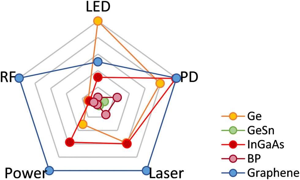 | ||
| Fig. 1 Application chart of single crystalline free-standing NBG NMs in the photodetector (PD), laser, light emitting diodes (LED), radio frequency (RF) and power electronics based on the number of publications. Data are collected by keyword search from Web of Science (year of search: 2022). | ||
2D materials are atomically thin crystalline solids, existing in the form of one or few-layered sheets where each layer is bound by van der Waals (vdW) force. So far, 2D materials have aroused tremendous research interest due to their outstanding and unique material properties such as large surface area, nanoscale thickness, flexibility, and remarkable optoelectronic properties. These material properties allow 2D materials to be considered as one of the most promising candidates for the applications of optoelectronic devices. Graphene, the firstly discovered 2D material, has been extensively studied and applied to versatile optical and electronic devices because of its exceptional thermal and electrical conductivity with flexibility.34–36 Black phosphorous (BP) is an emerging 2D material that has distinctive material properties, which include not only high conductivity and carrier mobility but also tunable direct band-gap, unlike graphene. This tunable band-gap of BP enables a wide range of devices applications.37,38
Free-standing NBG NMs are promising material platforms for various applications. However, there is no comprehensive review focused on NBG NMs so far. Therefore, in this paper, we provide a comprehensive review on the recent progress of NBG NMs. Representative NBG NMs are discussed, including Ge, GeSn, InGaAs, and 2D materials (BP and graphene). Our review covers material characteristics, fabrication methods, and device applications. Finally, we present the conclusion and major challenges and future perspectives on single crystalline NBG materials.
2. Ge and GeSn nanomembranes
NMs are monocrystalline structures with a thickness of a few hundred nanometers, leading to the advantages of flexibility, bendability, and light weight. The main difference from thin films is that NMs can exist as a free-standing form, either at certain critical stages of their growth or processing or at steps with the final device-integrated form.Ge has been widely explored as a platform for optoelectronic devices due to its CMOS capability. Although it is an indirect band-gap semiconductor, the energy difference between the lowest indirect L and direct Γ valleys is only 136 meV as indicated in Fig. 2(a). Additionally, the introduction of tensile strain or incorporation of Sn can effectively compensate for the small difference, which turns Ge into a direct band-gap semiconductor.54,55 Numerous studies have shown that the band-gap structure of Ge can be modulated from indirect to direct by applying tensile strain. On the other hand, the incorporation of Sn into Ge also changes the electronic band structure by shrinking L and Γ valleys simultaneously while Γ valleys drop faster than L valleys (Fig. 2(b)). As shown in Fig. 2(c), there is a crossover point of band-gap transition when Sn composition increases to 8%, indicating that 8% of Sn successfully changes Ge to a direct band-gap semiconductor under no external strain conditions. However, the Sn content is limited by the compressive strain resulted from lattice mismatch between Sn and Ge.
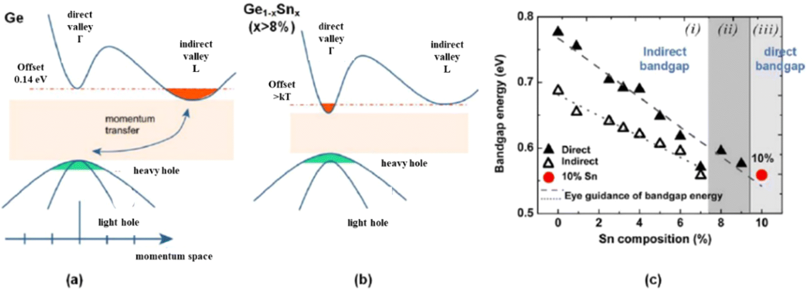 | ||
| Fig. 2 Energy band structure of (a) undoped Ge bulk with indirect bandgap and (b) GeSn alloying with Sn composition higher than 8% with direct bandgap without mechanically introducing strain. (c) The indirect-to-direct transition of GeSn band-gap energy as a function of Sn composition.56 | ||
2.1. Strategies to fabricate GeSn NMs
Typically, the formation of GeSn NMs begins with GeSn on an insulator (GeSnOI) or GeSn on an Si-on-insulator (SOI) platform. As illustrated in Fig. 3, wet and dry etching are the most common methods to fabricate GeSn NMs. To give an example of GeSnOI, (Fig. 3(a)) array patterns of etching holes (size of 3 × 3 μm2 and distance of 50 μm) are created on the cleaned substrates followed by reactive ion etching (RIE) to etch down to the sacrificial layer. These etching holes act as a pathway for etching solutions to reach the oxide layer, which leads to rapid and uniform undercut. Subsequently, SiO2 sacrificial layer is removed by dipping in hydrofluoric acid (HF, 49%), releasing top GeSn/Ge template layers. The released NMs are then transfer printed to a SU-8 coated polyethylene terephthalate (PET) substrate using a direct flip transfer method. Another transfer printing process using a polydimethylsiloxane (PDMS) stamp can also replace this step as long as NM is present as the uppermost layer. Finally, the layers on top of GeSn (e.g., buffer Ge and Si) are etched by an SF6-based RIE to create fully relaxed flexible GeSn NMs.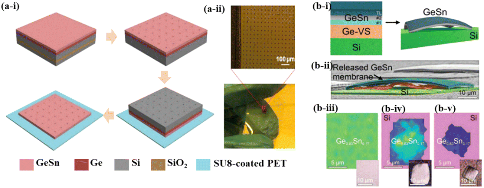 | ||
| Fig. 3 Schematic illustration of the most common methods used to fabricate GeSn NMs. (a) Wet etching:13 (i) Preparation of strain-free GeSn NMs by patterning an array of etching holes followed by RIE, HF undercut, and transfer printing. (ii) Optical images of GeSn NMs on PET with its magnified microscopic image. Reproduced with permission from ref. 13. Copyright 2020, IOP Publishing. (b) Dry etching:57 (i) Fabrication of GeSn NMs by anisotropic etching of GeSn sidewalls using Cl2-based plasma, followed by CF4-based selective etching of buffer Ge layer. (ii) SEM of a solitary released GeSn membrane and (iii–v) Raman spectroscopy maps for an as-grown GeSn layer, partially suspended and fully released GeSn membrane, respectively. Reproduced with permission from ref. 57. Copyright 2020, Wiley-VCH. | ||
Fig. 3(b) shows another approach to obtain GeSn NMs namely a dry release approach. The starting material is GeSn on Ge virtual layer grown on an Si substrate. It begins with the anisotropic Cl2-based RIE of the GeSn sidewalls, followed by a CF4-based selective etching of the Ge layer. Although the process is relatively simple, the size of NMs (20 × 20 μm2) is limited by etching the selectivity between GeSn and the buffer Ge layer.
Etching holes facilitate the wet etching process and therefore no obvious residuals exist due to the adequate chemical reaction and good selectivity. However, CF4-based dry etching with low selectivity results in a damaged GeSn surface due to over-etching. By changing the power and pressure of RIE, the residual can be reduced by the enhanced selectivity. Although wet and dry etchings are promising to release Ge/GeSn membranes form source wafers, it is still a great challenge to fabricate large-size strain-free GeSn membranes with high Sn content and good surface quality. Moreover, the fabrication of ultrathin GeSn membranes with a thickness of less than 100 nm is also challenging. A higher undercut temperature and a more diluted etchant provide a feasible way to produce large-sized uniform membranes by promoting the contact between the etchant and the sacrificial layer.
2.2. Strain engineering
Strain engineering is an essential research topic for GeSn NMs because their ultra-thin thickness (nm) enables the application of the strain by various methods. Practically, the methods used to apply strain can be divided into two categories depending on the type of applied strain: (i) internal strain generated during the growth process; (ii) external strain applied on well-prepared flexible GeSn NMs using mechanical testing equipment or home-made mechanical tools.Among versatile approaches for applying internal strain, one of the most popular methods is to utilize high-stress layers, which act as an extrinsic stressing agent to introduce biaxial tensile strain.58 C. S. Fenrich et al. deposited 260 nm SiNy on Ge0.934Sn0.066 multiple quantum well microdisk, creating a direct band-gap by elimination of local biaxial strain. Another form of internal strain engineering is the rolling up, which is used to fabricate micro-resonators. Fig. 4(b) illustrates the rolling up method where GeSn NMs were rolled up from the sample with pre-defined U-shape patterns formed by lithography and RIE and subsequent HF etching. The undercutting process releases NMs from the substrates by self-rolling from the lower side of the U-shape, which is resulted from different strain in each layer. The fabricated micro-resonator with this structure showed a high quality factor (Q factor) of up to 800.59
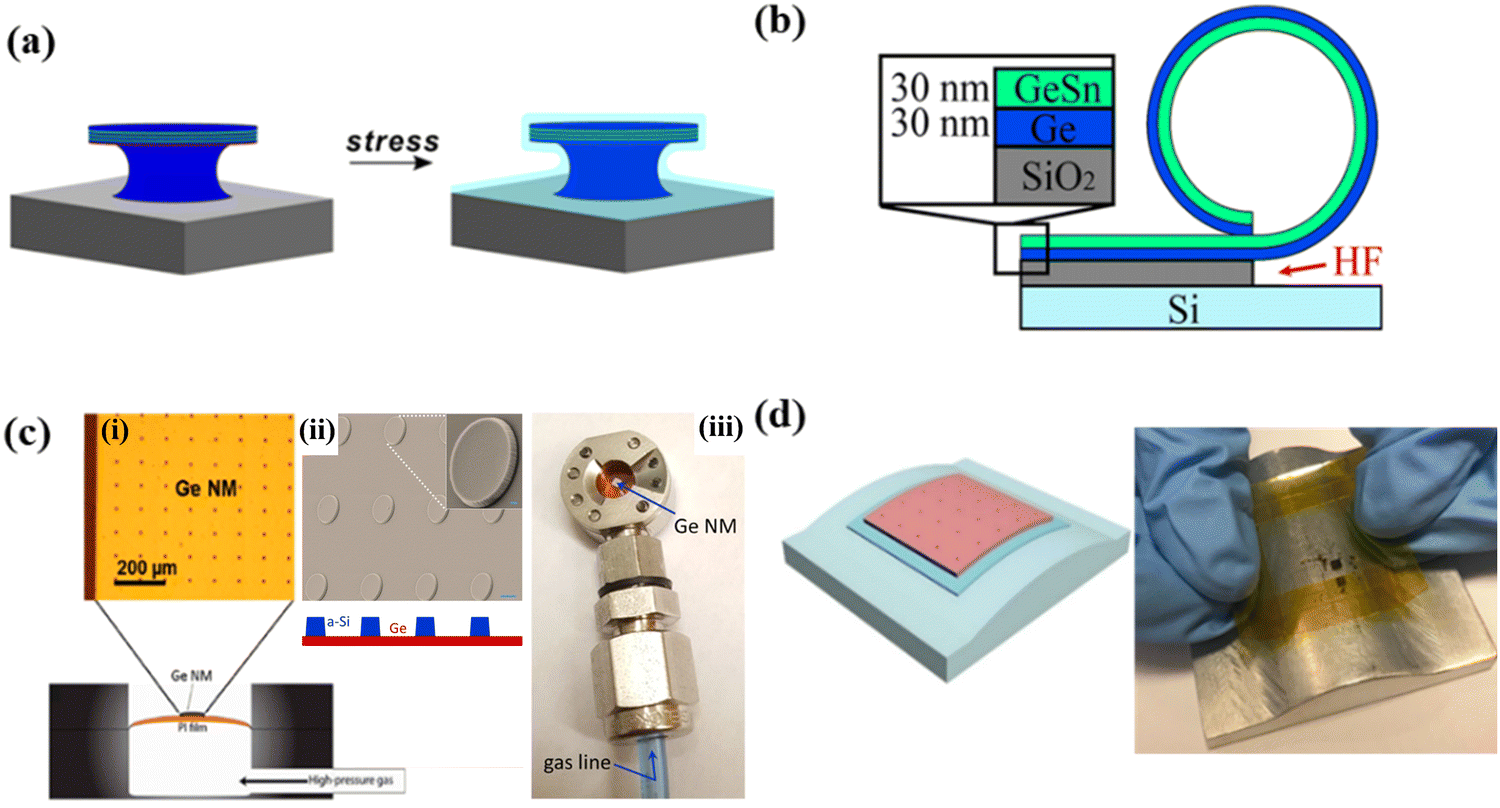 | ||
| Fig. 4 Various strain-engineering strategies for GeSn NMs: (a) Tensile strained GeSn microdisk using high-stress SiNy stressor layer.58 Reprinted with permission from ref. 58. Copyright 2016, American Chemical Society. (b) A schematic diagram describing the rolling up procedure for the GeSn/Ge bilayer.59 Reproduced with permission from ref. 59. Copyright 2018, IOP Publishing. (c) (i) Schematic illustration of the experimental setup for biaxial tensile strained Ge NMs,60 (ii) SEM image with a schematic of a Ge NM coated with an a-Si pillar array, and a photograph of the pressure cell loaded with a Ge NM.61 Reproduced with permission from ref. 60 and 61. Copyright 2018, 2021, MDPI, American Chemical Society. (d) Schematic structure and optical image of flexible GeSn NMs where uniaxial strains are introduced by placing conformally on bending fixtures.62 Reproduced with permission from ref. 62. Copyright 2021, IOP Publishing. | ||
In addition to the techniques mentioned above, new technologies for applying strain on flexible Ge or GeSn NMs have been developed, as shown in Fig. 4(c) and (d). Fig. 4(c) shows the flexible Ge NM on polyethylene terephthalate (PET) film obtained by wet etching or dry etching, and herein, strains were introduced by externally applied gas pressure.60,61 Furthermore, uniform biaxial strain can be introduced through the expanding surface sphere, as the increase of the injected gas into the cavity causes the transformation of the top plane into a hemispherical shape. This technique could introduce various accurate minor strains, but the setup is complicated. Another approach to induce strain is to utilize bending fixtures with various radii. In this method, the bending fixture induces specific strain values by placing flexible NMs directly on the concave or convex fixture. The advantage of this approach is that the method is simpler than the gas pressure method. In addition, we can introduce uniaxial compressive strain to investigate its effect on the optoelectronic properties. However, one disadvantage is that only a specific strain can be introduced with one bending fixture, i.e. each bending condition requires one fixture. Using this bending fixture-based method, the applied strain can be evaluated using various analysis techniques. One example is Raman spectroscopy which has the advantageous feature that the system is highly sensitive with easy operation. Previously, several researchers have studied the relationship between the Raman shift and biaxial or uniaxial strain induced in flexible GeSn with different Sn compositions.62 Overall, internal or external strain can be easily introduced into GeSn by using stress layers or mechanical tools. However, the applicable area with a uniform strain is limited.
2.3. Applications of strain engineered GeSn nanomembranes
Although the thinness of GeSn NMs reduces absorption, the external strain and high Sn composition could offset the reduced absorption by modulating the band-gap structure, which enhances the absorption coefficient. Fig. 5(a) illustrates the fabricated flexible GeSn PDs and their performance characterization. Flexible Ge/GeSn NMs with 8% Sn content were released by wet etching, followed by mesa patterning and RIE to make rectangular mesa (90 × 100 μm2). Finally, interdigitated pads were deposited to form metal contacts (Fig. 5(a-i) and (a-ii)). As shown in Fig. 5(a-iii), dark current was increased by tensile strain, while it was slightly decreased by compressive strain. This trend was similar to photocurrent, showing that it was in accordance with strain-dependent modulation of the band-gap and corresponding change in absorption coefficient. In addition, responsivity at a wavelength of 2000 nm was enhanced to 3.68 mA W−1 by tensile strain, proving that high performance flexible NIR GeSn PD has been achieved.
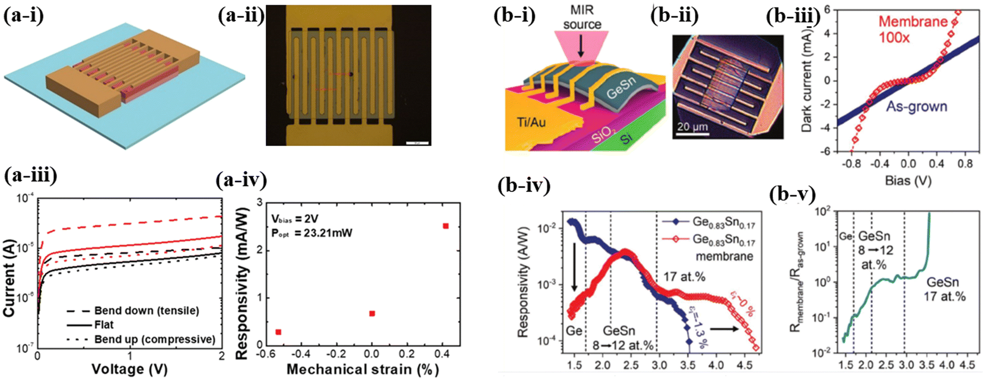 | ||
| Fig. 5 (a) Device structure and characteristics of flexible GeSn metal semiconductor metal (MSM) NM PD:19 (i) & (ii) Schematic and an optical image of the device structure, (iii) dark current and photocurrent under flat and bending conditions, and (iv) responsivity at 2000 nm as a function of mechanical strains. Reproduced with permission from ref. 19. Copyright 2020, Royal Society of Chemistry. (b) Structure and characteristics of GeSn NM PD on SiO2/Si: (i) & (ii) Schematic and an optical image of a fabricated device, (iii) dark current versus bias voltage, (iv) responsivity versus wavelength of as-grown and membrane devices, and (v) spectral responsivity ratio of the membrane and the as-grown GeSn device.63 Reproduced with permission from ref. 63. Copyright Copyright 2020, Wiley-VCH. | ||
The responsivities can be further improved to 148.5 mA W−1 at 1550 nm by integration of TiN.65 To expand its application into mid-IR (MIR) optoelectronic devices, a PD with an extended cut-off wavelength of 4.6 μm has been reported using fully released Ge0.83Sn0.17 NMs.57 A dry etching based release process drastically reduces the internal compressive strain caused by lattice mismatch. Then, the released GeSn NMs were transferred onto bulk SiO2/Si, and next, the device was fabricated by depositing interdigitated pad (Fig. 5(b-i) and (b-ii)). Although it is not intended for flexible device applications, it showed outstanding performance from the aspect of responsivity and cut-off wavelength. Fig. 5(b-iii) shows that the dark current of GeSn membrane PD was decreased by two orders compared to that of the as-grown GeSn PD because the highly conductive Ge-virtual substrate (VS)/Si stacking was replaced by an insulating substrate underneath. The responsivity of two PDs is similar in the wavelength range from 2.3 to 3.2 μm. At the longer wavelength region, the as-grown GeSn PD reached a sudden cut-off at 3.5 μm, while the membrane-based device exhibited constant responsivity up to 4.2 μm until reaching a cut-off wavelength of 4.6 μm due to strain relaxation. This study demonstrates that strain-relaxed GeSn NM is a great candidate for broad MIR range PDs. However, the flexible PDs exhibit high dark current, low quantum efficiency and slow response time compared with the rigid counterpart. The dark current can be suppressed by surface passivation processes combined with post-growth annealing to reduce the effect of defect trapping of charge carriers. Additionally, the device structure could also be optimized to reduce the carrier transit time to enhance responsivity and response speed. Light trapping through nanostructure including resonant cavity, photonic bandgap engineering, and plasmonic absorption enhancement can also be explored in this system to enhance the external quantum efficiency of the flexible GeSn PDs.
GeSn NM is a promising candidate material for lasers due to the direct band-gap structure. There has been substantial progress in laser technologies for achieving high-performance GeSn NM lasers with low threshold and high operating temperature. The first demonstration of Ge/GeSn/Ge quantum-well microdisk resonator with high Q factor was reported in 2014, laying the foundation for GeSn-based lasers.59,66 A GeSn laser with direct band-gap was achieved by undercut GeSn on Ge microdisk structures with additional strain introduced by silicon nitride stressor layers, leading to enhanced photoluminescence (PL) intensity and extended PL emission range to 3–5 μm.67 However, the PL intensity decreases dramatically by increasing temperature, which severely limits the device operating temperature as well as its real-life applications. V. Reboud et al. attributed the improvement of the lasing temperature up to 180 K using GeSn layers with a higher Sn composition of 16% and optimized crystalline quality.68 The operating temperature was further increased to 230 K by employing a thicker GeSn optically active layer and a stronger carrier confinement effect in a double heterostructure.69 A laser using GeSn photonic crystal membrane was demonstrated by Q. M. Thai et al. with fine performance. This approach has the potential for flexible device applications as the device was fabricated on the released layers rather than non-deformable microdisk.70 Flexible laser made on Ge NM integrated with photonic-crystal cavities with Si-pillar arrays have shown PL intensity increase due to strong optical coupling between Ge NM and the cavities. This device still preserves the mechanical flexibility advantage of NMs.71 Recently, some breakthroughs have been made in the field of low threshold laser. A. Elbaz et al. reported an ultra-low threshold laser with 0.8 kW cm−2 based on the GeSn substrate with low Sn content.72 A higher Sn composition makes it easier to realize direct band-gap lasers, but it also generates defects that degrade the laser performance. Therefore, finding an appropriate balance between defect engineering and Sn composition is the key to reducing the threshold of GeSn laser.73 The key parameters of GeSn NMs based lasers are summarized in Table 2.
| Sn content | GeSn layer | Strain | Method | Wavelength | Threshold | Temperature |
|---|---|---|---|---|---|---|
| 10.7%67 | 40 nm | Tensile | SiNx stressor layer | 3000 nm | low | 20 K |
| 16%68 | 400 nm | Zero | Micro-disk | 3100 nm | 377 kW cm−2 | 180 K |
| 16%69 | 850 nm | Compressive | Micro-disk | 3200 nm | 790 kW cm−2 | 230 K |
| 16%70 | 520 nm | Compressive | Step graded GeSn buffer | 2880 nm | 227 kW cm−2 | 15 K |
| 5.4%72 | 300 nm | Tensile | SiNx stressor layer | 2500 nm | 0.8 KW cm−2 | 100 K |
| 7%73 | 500 nm | Compressive | Micro-disk | 2300 nm | 10 kW cm−2 | 25 K |
For MIR optoelectronic devices, many researchers have attempted to utilize other Group IV materials, such as Ge waveguide integrated MIR devices. In 2016, Wei et al. demonstrated Ge-on-SiN waveguides with large core-clad index contrast by wafer bonding and layer transfer technique. They employed chemical mechanical polishing (CMP) to remove the misfit dislocation between Ge and Si after the layer transfer process. The results showed that the fabricated waveguide had a propagation loss as low as 3.35 dB cm−1 at the wavelength of 3.8 μm.74 Advanced material platform was proposed recently by W. Li et al., with an optimized structure using GaF2 and Y2O3 as cladding where the waveguiding performance was enhanced by a larger difference of refractive indexes between Ge and insulator. As a result, the proposed Ge waveguide platform showed improved performance by covering the MIR wavelength range up to 13 μm.75
3. InGaAs NMs
3.1. Fabrication process
InGaAs, a III–V semiconductor with a band-gap of 0.75 eV, is the most common material used for commercial NIR photodiode, taking advantage of room temperature operation with high electron mobility, external quantum efficiency, sensitivity, and fast response time.76 Despite the competitive advantages of InGaAs, narrow detection range and large dark current restrict its application in optical communication. Therefore, flexible InGaAs NMs provide a means of extending their detection range by band-gap modulation via strain engineering. However, little research on InGaAs NMs has been carried out mainly due to the difficulties in releasing high-quality InGaAs NMs.Similar to the fabrication of GeSn NMs, InGaAs NMs can be released by removing the sacrificial InAlAs layers using hydrochloric acid (HCl). As shown in Fig. 6, wrinkled InGaAs NMs were fabricated by selective wet etching followed by vacuum-induced stretching of locally constrained InGaAs NMs. This technique introduces biaxial strain and therefore provides an approach to modulate carrier mobility and band structure of InGaAs NMs. However, it has the limitation in the choice of the sacrificial layer. In general, InGaAs layer was grown on AlAs/InP substrate using AlAs as a sacrificial layer. Although AlAs could offer high etching selectivity over both the InP substrate and the functional InGaAs layer in HF solution, the lattice mismatch (3.6%) with InP makes it difficult to form high quality InGaAs layers.
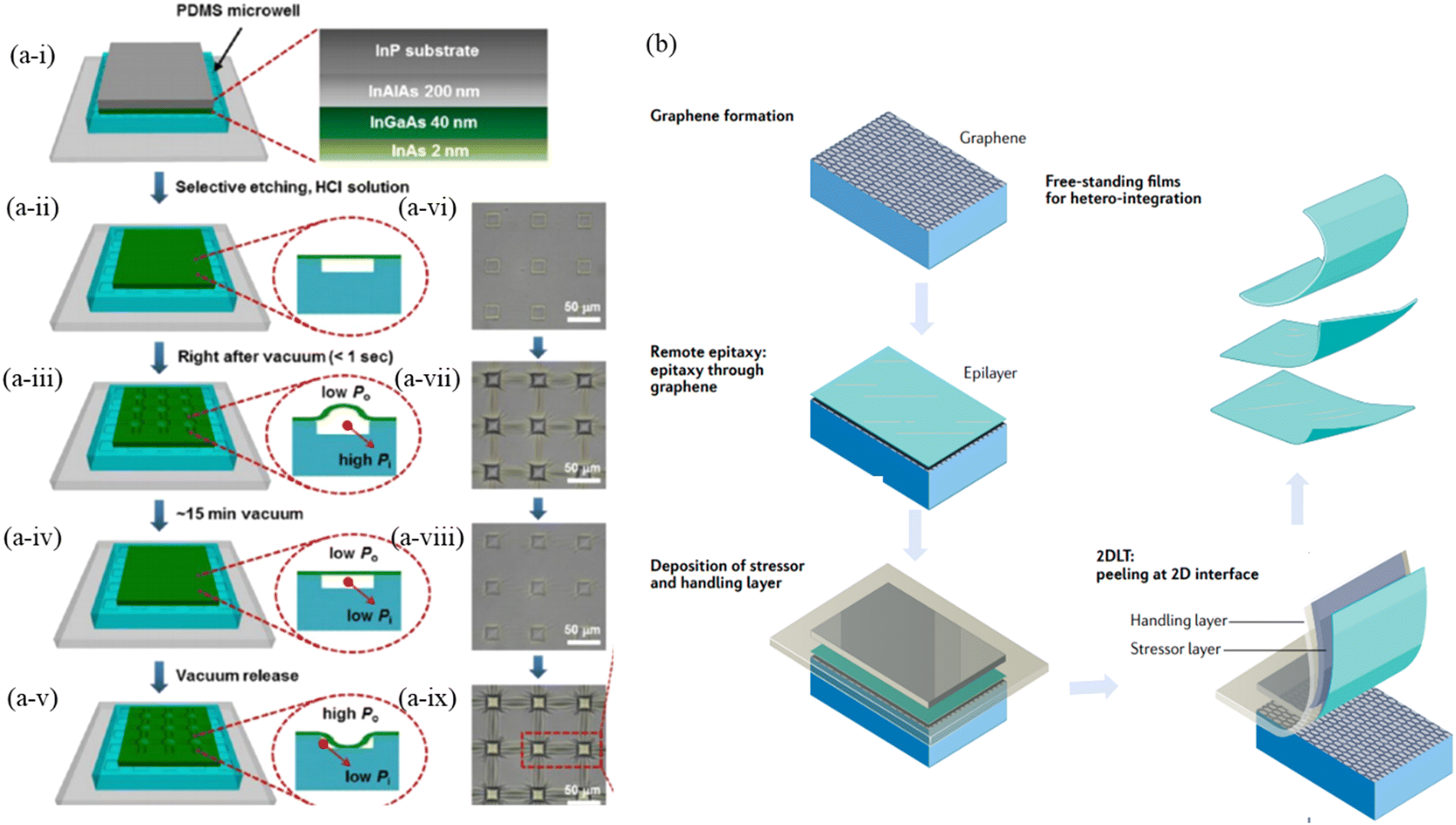 | ||
| Fig. 6 (a) The vacuum-induced wrinkling of InGaAs NMs on polydimethylsiloxane microwell array: (i–v) Schematic illustration of the fabrication procedure. (vi–ix) A series of optical microscope (OM) images of InGaAs NMs during the vacuum-induced wrinkling process: (vi) before the vacuum process, (vii) right after the vacuum process, (viii) ∼15 min after the vacuum process, and (ix) right after the vacuum release.77 (b) Remote epitaxy and layer transfer process.78 Reproduced with permission from ref. 77 and 78. Copyright 2014, 2022, American Chemical Society, Springer Nature. | ||
Another emerging approach called remote epitaxy has been proposed to overcome the limitation and achieve high-quality single crystalline NMs. GaAs was epitaxy grown on graphene coated bulk GaAs substrate.79,80 The ultrathin graphene layer allows remote interaction between substrates and epilayers, leading to the formation of crystalline epilayers that continues the substrate crystals.81,82 GaAs NMs were released after removing graphene layer by wet or dry etching.
3.2. Applications of InGaAs nanomembranes
Recently, InGaAs NMs were developed for applications in optoelectronic devices, such as PDs,83,84 LEDs,85 and field effect transistors.86 For example, D. Fan et al. demonstrated a thin-film InGaAs p–i–n PD array fabricated on a thin and flexible polyimide Kapton substrate.87 The array was transformed into a cylindrical shape to achieve a 360° (i.e., 2π) in-plane field of viewing (FOV). High-performance flexible InGaAs PDs integrated with waveguide were demonstrated, exhibiting a low noise equivalent power of 0.02 pW Hz1/2 at room temperature and the telecommunication C-band. Moreover, significant improvements include a large linear dynamic range over 70 dB and 3 dB bandwidth of 1.4 GHz, all of which set new records for flexible detectors, as shown in Fig. 7(a).88 J. Shi et al. also reported InGaAs/InAlAs high electron mobility transistors transferred onto a flexible Kapton substrate employing the adhesive bonding technique. The effect of mechanical bending conditions on electrical performance has been also investigated in static and dynamic regimes.89 Although InGaAs membrane-based optoelectronic devices outperform Group IV membrane-based devices due to its direct bandgap, the CMOS compatibility and cost are still obstacles for the commercialization. To overcome this problem, a monolithic InP/SOI platform has been developed, where both dislocation-free InP submicron wires and large-dimension InP membranes are selectively grown on (001) SOI wafers and intimately placed with the Si device layer. The InGaAs quantum wells or InAs quantum dots could be selectively regrown on top of the NMs.90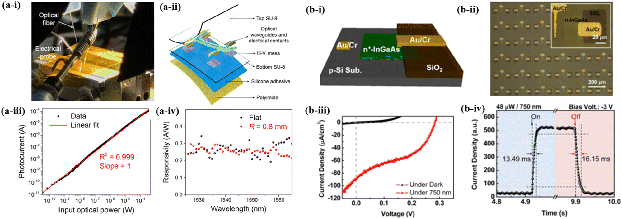 | ||
| Fig. 7 InGaAs NM optoelectronic device applications: (a-i) Photo during the measurement, (a-ii) schematic structure, (a-iii) double logarithm plot showing the linear dynamic range, (a-iv) spectral response across C-band and bent states of flexible waveguide-integrated InGaAs NM PD.88 Reproduced with permission from ref. 88. Copyright 2018, Optical Society of America. (b-i) Schematic device structure, (b-ii) Microscopic image of the device, (b-iii) photovoltaic characteristics, and (b-iv) the enlarged current response time at −3 V reverse bias under the 750 nm (48 μW) light illumination of InGaAs NM/Si heterojunction PD.91 Reproduced with permission from ref. 91. Copyright 2016, American Chemical Society. | ||
Another promising application of narrow band-gap NMs is broadband heterojunction diodes through van der Waals (vdW) bonding, which is of great importance in high-capacity optical communication. Conventional approaches to fabricate heterojunctions such as epitaxial growth or wafer bonding have problems of inferior interface quality due to the lattice mismatch and thermal expansion coefficient mismatch. Thus, heterojunction formed by transfer printed NMs on dissimilar layers is a useful approach to avoid such mismatch issues. High-performance broadband InGaAs NM/Si heterojunction PDs that cover the detection range from 450 to 1250 nm have been demonstrated. The devices exhibited a high rectification ratio of 7.73 × 10⁴ at ±3 V, a low leakage current of 7.44 × 10⁻⁵ A cm−2 at −3 V, and fast response times of 13–16 ms, owing to the high-quality interface enabled by the transfer printing technique (Fig. 7(b)).91 This technique has been also applied on GeSn/Si heterostructures formed by transfer printing of Si NMs on GeSn layers with various Sn contents. An increase in the Sn content extended the detection range of GeSn/Si PDs up to 2100 nm.92 Y. Lee et al. have demonstrated an n-InGaAs/BP diode by adopting double-times transfer printing of each NMs onto a SiO2/Si substrate via PDMS stamping.93 This device offers nonvolatile-memory properties through charge trapping in the native phosphorus oxide, exhibiting unique diode characteristics which are gate-controllable and programmable. These multifunctional properties provide numerous potential applications such as novel advanced logic circuits, controllable electric transformers, and neuromorphic devices. Therefore, the transfer printing technique can be more desirable than other approaches to achieve high-quality heterostructures with dissimilar materials.
4. Black phosphorus
4.1. Fabrication process
BP, one of the most promising NBG 2D materials, is a layered plane of phosphorus monolayer (called phosphorene) with an anisotropic puckered honeycomb structure. The unique material properties of BP include high electron mobility (1000 cm2 V−1 s−1), on/off current ratio (<105),46,49 anisotropic transport, and tunable direct band-gap (0.3 eV in bulk to 2.0 eV in a single layer).94,95 Owing to these excellent intrinsic optoelectronic properties, BP has been applied in a wide range of optical and electrical devices such as lasers, PDs, transistors, and logic inverters. Contrary to the NMs, which typically use wafer-scale semiconductor-on-insulator platforms, the fabrication of 2D material NMs relies on exfoliation from bulk crystalline materials using either top-down exfoliation or bottom-up direct growth techniques.Since the first successful synthesis of bulk BP in 1914 by Bridgman,96 numerous studies have reported high-quality bulk BP from red or white phosphorus. The high-pressure methods such as the Bridgman and ball milling methods have disadvantages in that they require over 1 GPa pressure with a limitation in the size of synthesized BP (micrometer scale).97–99 Thus, new approaches have been developed to obtain millimeter-sized bulk BP under low pressure, such as BP synthesis with mercury catalyst,100 and bismuth-flux,101,102 or chemical vapor transport.103,104 The synthesized bulk BP is then used to isolate thin-film BP NMs using isolation techniques, such as mechanical exfoliation, liquid-phase exfoliation (LPE), and electrochemical exfoliation (ECE),105–107 and herein, the quality of bulk BP is of utmost importance.
The mechanical exfoliation, which is to peel few-layer BP from bulk phosphorus by overcoming vdW attraction between bulk phosphorus flakes, includes micromechanical cleavage with adhesive tape46,49 and additional subsequent plasma thinning (Fig. 8 (a)).108,109 For LPE, BP is produced by sonicating dispersed liquid of bulk BP in a solvent followed by centrifugation. Compared to other processes, LPE is suitable for mass production because of its advantages of low-cost, simple, and efficient fabrication. Since the first LPE-synthesized BP was demonstrated by J. R. Brent et al. using N-methyl-2-pyrrolidone (NMP) solvent,110 many researchers have shown successful synthesis of BP using LPE by applying multiple solvents: organic solvents such as benzonitrile, DMI, PVP, MF,111 dimethylformamide (DMF), dimethyl sulfoxide (DMSO),112N-cyclohexyl-2-pyrrolidone (CHP),113 IPA,114,115 and a non-organic solvent such as distilled water.116 Furthermore, advanced LPE using ionic liquids or solvothermal reactions also have been developed for large-scale, efficient, and facile fabrication.117,118 For the ECE approach, thin-film BP is isolated from an electrode with bulk BP crystal by applying the voltage between two electrodes, triggering redox reactions between water molecules, electrolytes, and electrodes, and weakening vdW force. (Fig. 8(b)) After the first ECE trial by M. B. Erande et al. who demonstrated anodic BP ECE using NA2SO4 electrolyte in H2O,119 numerous studies have been made with diverse combinations of electrolyte and solvent: anodic ECEs of H2SO4 in H2O,120 [EMIM][BF4] in MeCN,121 [BMIM][PF6] in MeCN,122 cathodic ECEs of TBAP in DMF,123 TAA in DMSO,124 TBA-HSO4125 in PC, and PEAP in PC,126 and bipolar ECEs.127,128 Here, while anodic ECE resulted in a dimension of 0.5–5 μm and thickness of 1–10 nm because of the oxidation of BP at the anodic electrode, cathodic ECE has shown a larger dimension over 10 μm and thinner thickness of 0.76–10 nm. Nevertheless, the top-down approaches are considered unsuitable for industrial applications due to the small size of exfoliated BP.
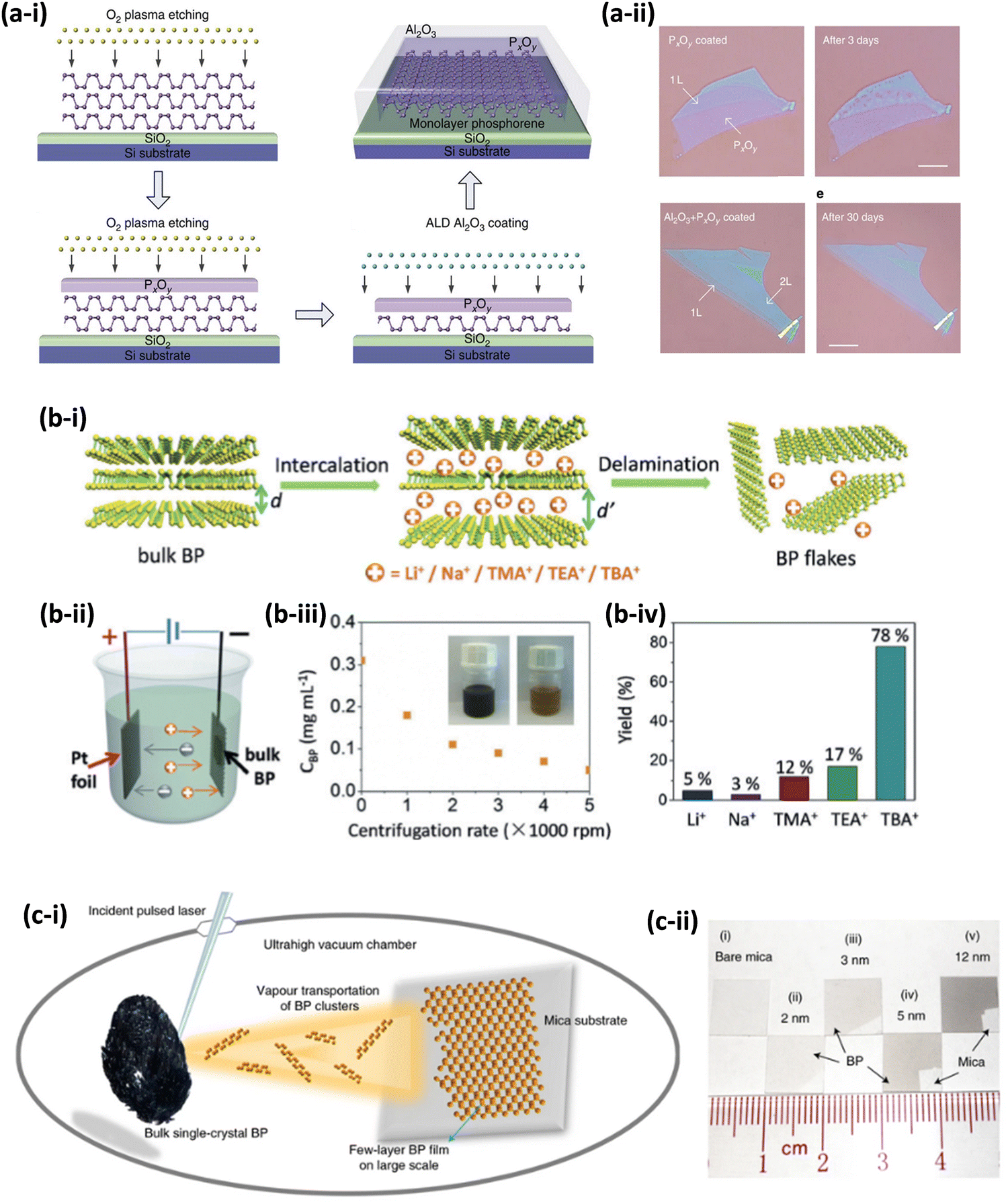 | ||
| Fig. 8 (a) Mechanically exfoliated black phosphorus (BP) on a SiO2/Si substrate treated with O2 plasma etching: (a-i) schematic illustration of the preparation process, and (a-ii) OM images of single-layer BP covered by PxOy or PxOy/Al2O3 capping layer before and after several days.109 Reproduced with permission from ref. 109. Copyright 2016, Springer Nature. (b): Electrochemically exfoliated BP: (b-i) Schematic delamination procedure, (b-ii) Experimental setup, (b-iii) Concentration of BP as a function of centrifugation rate, and (a-iv) Delamination yield as a function of intercalating cations.125 Reproduced with permission from ref. 125. Copyright 2016, John Wiley-VCH. | ||
As an alternative approach for wafer-scale mass production, bottom-up methods have been developed which is a direct-growth approach of thin-film BP by chemical vapor deposition (CVD),129 pulsed laser deposition (PLD),130,131 gas-phase transformations,132 and solid–vapor–solid transformation.133 Although CVD is widely used for 2D material synthesis, the CVD approach exhibited poor performance due to high defect density and poor electrical and optical properties. Although PLD also showed the successful synthesis of BP on a centimeter scale) the method is unsuitable for mass production due to its high cost as well as the low carrier mobility of synthesized BP. Furthermore, there is an additional issue with utilizing few-layer BP at the device level which is its poor stability. High stability can be achieved by applying physical or chemical methods after the preparation of a few-layer BP. The physical method is to cover BP by a passivation layer such as oxides such as Al2O3,134 SiO2,135 TiO2 nanoparticles,136 or 2D materials (e.g. graphene and hBN).137 The chemical method improves stability through the modification of molecules138 or metal ions.139,140 In summary, utilization of BP in optical and electrical devices still has some challenges due to difficulties in synthesizing highly crystalline and large-size BP, as well as improving stability in the air.
4.2. Applications
Using the excellent flexibility of BP reported by Q. Wei et al.,141 the first flexible BP transistor has been demonstrated by W. Zhu et al.142 As described in Fig. 9(a), the device was fabricated by mechanical exfoliation method and exhibited outstanding carrier mobility of 310 cm2 V−1 s−1 as well as robust device performance after 5000 cycles of bending with 2% tensile strain. Furthermore, J. Miao et al. showed flexible NIR BP PDs which have high responsivity of 53 A W−1 under 16.5 W cm−2 laser illumination (λ = 830 nm).143
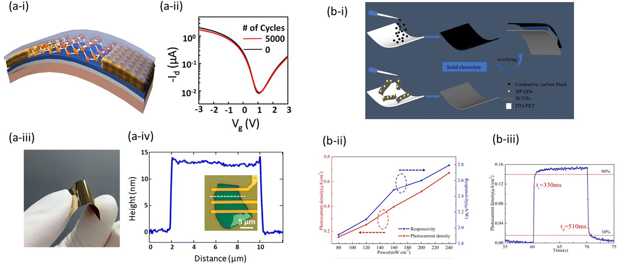 | ||
| Fig. 9 (a) Flexible BP FETs on a flexible PI substrate: (i) schematic illustration, (ii) I–V characteristics, (iii) Photograph of the device, and (iv) AFM height profile of a few-layer BP flake showing thickness of 13 nm.142 Reproduced with permission from 142. Copyright 2015, American Chemical Society. (b) Flexible Bi nanosheets-BP quantum dots PDs: (i) Device fabrication process, (ii) photocurrent density and responsivity, and (iii) temporal response.145 Reproduced with permission from 145. Copyright 2021, American Chemical Society. | ||
Also, a combination of other 2D materials showed an improved photodetection performance. Recently, H. Kim et al. demonstrated flexible and strain-tunable IR optoelectronic devices based on BP-MoS2 heterostructures using mechanical exfoliation.144 Here, different optoelectronic devices including PD and LED were demonstrated and they showed high detectivity of 5.97 × 109 cm H w1/2 W−1 at 4.0 μm and 8.45 × 109 cm Hz1/2 W−1 at 2 μm under compressive and tensile conditions, respectively. Y. Zhou et al. also exhibited a superior flexible PD based on bismuth nanosheets–BP quantum dots heterojunctions by sonication-assisted LPE, achieving a photocurrent density of 4.6 μA cm−2 at an applied voltage of 0.8 V, and 100 nA cm−2 without external voltage.145 (Fig. 9(b)) For the bending test, the device performance revealed the photocurrent density attenuation of 15% after 2000 times of bending and 8.8% under a bending angle of 60°.
There has been a recent progress in MIR LEDs using BP-based heterostructures. X. Zong et al., demonstrated BP-TMDC heterostructure using either WSe2 or MoS2.147 The BP-based vdWH LED integrated with WSe2 or MoS2 showed an ∼200% enhancement of the PL intensities in the MIR region due to efficient energy transfer between BP and WSe2, and MIR lasing at room temperature, respectively. J. Wang et al. developed the BP/MoS2 MIR LEDs emitting at 3.68 μm at room temperature. It showed enhanced outcoupling efficiency via the use of low-index or metallic substrate, as well as further improved quantum efficiency via heterostructure.148 Recently, H. Kim et al. demonstrated flexible BP MIR LEDs with strain-tunable band-gap characteristics, and observed PL peak shift from 5.5 to 3.2 μm under compressive and tensile strain, respectively.144
In this review, we focus on BP's applications in flexible or optoelectronic devices. Although it is not covered in depth, there have been a large number of publications on BP-based electronic devices including transistors, being considered as the primary application area.149
5. Graphene
5.1. Fabrication process
Graphene, which is the first discovered 2D material, is a solitary single layer of carbon atoms bonded in a hexagonal honeycomb lattice. The unique material properties of graphene include high carrier mobility (200![[thin space (1/6-em)]](https://www.rsc.org/images/entities/char_2009.gif) 000 cm2 V−1 s−1),150 thermal conductivity (5000 W m−1 K−1),151 transparency (97.6%, white light),152 Young's modulus (1.0 TPa),153 zero band-gap (0 eV),40 and novel intrinsic physical properties such as high mechanical, electronic, and thermal transport. Due to its superior properties, a wide range of applications have been discovered in semiconductor devices such as transistors, sensors, supercapacitors, batteries, PDs, solar cells, LEDs, and biomedicines. Furthermore, as a pioneering 2D material, the graphene has been produced by various techniques, which can be divided into two categories; top-down and bottom-up.154,155 Top-down methods where graphene is isolated from graphite include mechanical exfoliation, LPE, ECE, reduction of graphene oxide (GO), and laser ablation. For the bottom-up approaches, graphene can be directly synthesized on a substrate by CVD, epitaxial growth, arc discharge, and self-assembly.
000 cm2 V−1 s−1),150 thermal conductivity (5000 W m−1 K−1),151 transparency (97.6%, white light),152 Young's modulus (1.0 TPa),153 zero band-gap (0 eV),40 and novel intrinsic physical properties such as high mechanical, electronic, and thermal transport. Due to its superior properties, a wide range of applications have been discovered in semiconductor devices such as transistors, sensors, supercapacitors, batteries, PDs, solar cells, LEDs, and biomedicines. Furthermore, as a pioneering 2D material, the graphene has been produced by various techniques, which can be divided into two categories; top-down and bottom-up.154,155 Top-down methods where graphene is isolated from graphite include mechanical exfoliation, LPE, ECE, reduction of graphene oxide (GO), and laser ablation. For the bottom-up approaches, graphene can be directly synthesized on a substrate by CVD, epitaxial growth, arc discharge, and self-assembly.
Mechanical exfoliation is one of the earliest types of graphene synthesis methods, consisting of repeated attach-and-peel-off steps using a sticky tape, also well known as the Scotch tape method discovered by K. S. Novoselov et al.40 (Fig. 10(a)) Not only it is a cost-effective and easy method, but also the material properties of synthesized graphene are remarkable including high carrier mobility and ambipolar field effect.156 However, the size of mechanically exfoliated graphene is small and inapplicable for mass production, arousing a need for a large-area synthesis method that is economical and applicable for industry.
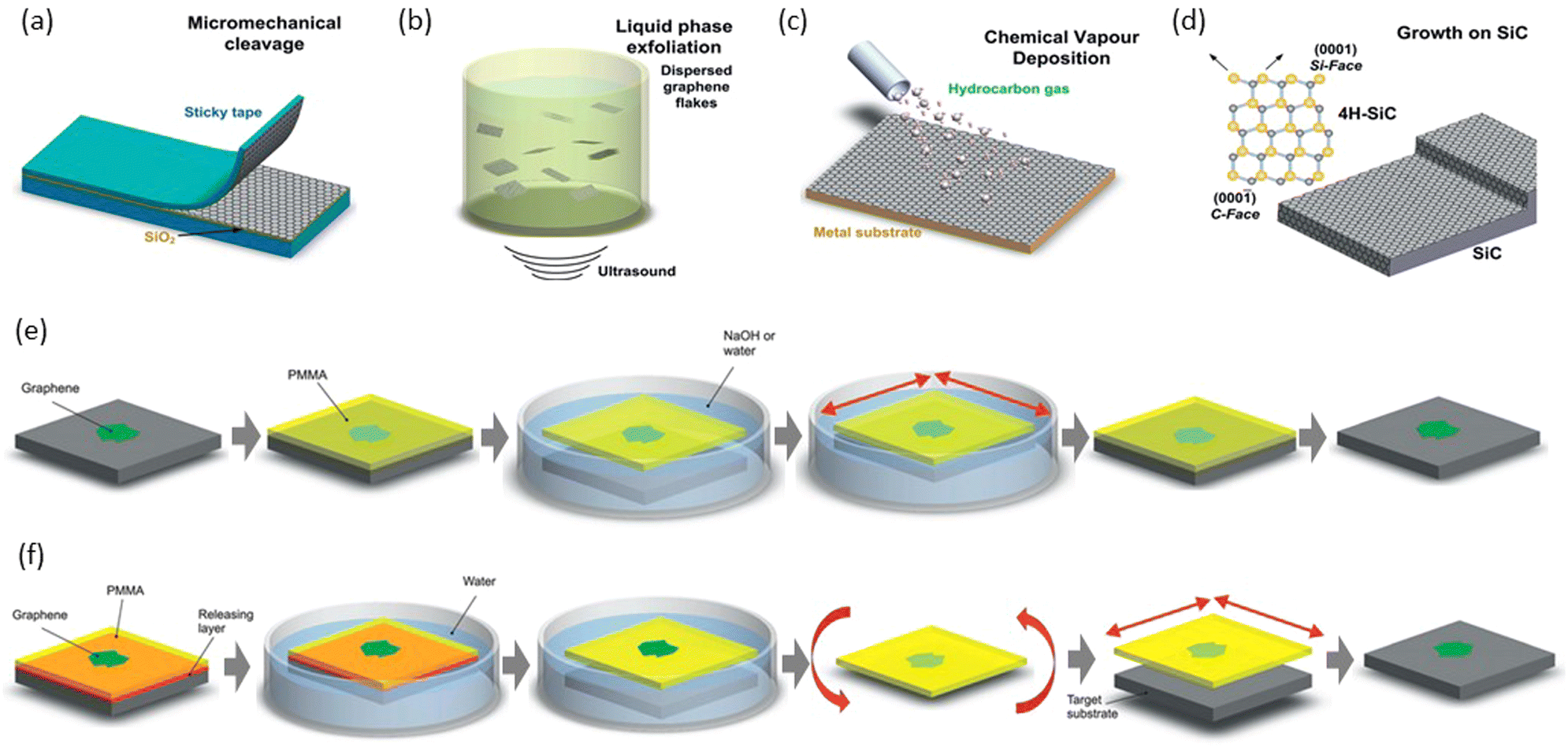 | ||
| Fig. 10 Graphene synthesis and transfer methods: (a) mechanical exfoliation, (b) liquid phase exfoliation, (c) chemical vapor deposition, (d) growth on SiC, (e) wet transfer and (f) dry transfer method.155 Reproduced with permission from ref. 155. Copyright 2012, Elsevier Ltd. | ||
Chemical exfoliation includes LPE, reduced GO (rGO), and ECE. LPE which originated in the 1860s157–159 is a method that isolates graphene from graphite in aqueous solutions by sonication,160 high-shear mixing, or jet cavitation. So far, sonication-assisted LPE has been vigorously studied under various solvent and sonication conditions161 (Fig. 10(b)). However, due to the low yields and high energy consumption of sonication-assisted LPE, the emerging LPE methods using high-shear mixing and jet cavitation are preferred over sonication, to be more applicable for production of large-size graphene. Here, high-shear stress can be generated by different methods such as ball milling,162 tube rotation,163 and rotor/stator.164 The jet cavitation method is a green process that can produce graphene in a short time by forcing fluids under pressure to flow through a narrow microchannel, also called the microfluidization method.161 Another chemical exfoliation approach is to chemically reduce GO, forming rGO by strong acids salts such as KMnO4, NaNO3, and H2SO4. This method is also widely used and is well known as Hummers’ method.165 In addition, there have been tremendous studies that showed the successful synthesis of graphene by the ECE approach with additional sonication.166,167 From the series of studies on ECE, it was found that the sonication-assisted ECE approach can improve the graphene quality and minimize defects under high temperature and ultrasonic waves, becoming the commonly used approach in the science and industrial fields.34 Laser ablation is an emerging top-down method, having strong advantages in that the process is environmentally friendly, stable, patternable, and applicable on flexible substrates without the usage of harmful reactants. Since the first demonstration of graphene synthesis by laser ablation on polymer films reported by J. Lin et al.,168 laser-ablation synthesis methods using various sources such as wood,169 cork,170 and paper,171 and a wide range of lasers such as UV172 or Vis radiation,173 have been reported.
CVD is an ideal method capable of industrial production of high-quality and large-area graphene. The first CVD-grown graphene was reported by Q. Yu et al., exhibiting graphene synthesis on Ni substrate using CH4, H2, and Ar gases at 1000 °C.174 So far, various metallic elements including Ni,175 Cu,176 Pd,177 Pt,178 and Ir179 were utilized as a substrate for CVD-grown graphene for a metal catalytic effect (Fig. 10 (c)). CVD-grown graphene has led to superior material properties such as large size single-crystalline graphene and outstanding charge carrier mobility of 350000 cm2 V−1 s−1 at room temperature. However, the limitations of CVD lie in its high cost and challenging transfer onto other substances. Another bottom-up method is the epitaxial growth method through the graphitization of silicon carbide (SiC)180,181 or hexagonal boron nitride (hBN),182 which is capable of graphene production with high crystalline quality and charge carrier mobility of ∼27000 cm2 V−1 s−1 (Fig. 10(d)). However, the disadvantages of the epitaxial growth method lie in its high-cost SiC substrate and limited size of the synthesized graphene.
After the production process, graphene is transferred through a wet or dry process (Fig. 10(e and f)). As shown in Fig. 10(e), a typical wet transfer is conducted by the following process steps; deposition of a polymethyl methacrylate (PMMA) film on graphene by spin coating; detachment of the PMMA film by wet chemicals; attachment of graphene/PMMA film to a target substrate; drying; dissolution of PMMA by acetone to release graphene on the substrate. On the other hand, graphene can be transferred through dry transfer, as depicted in Fig. 10(f); exfoliation of graphene on water-dissoluble polymer covered by PMMA; floating the sample in water; dissolution of the water-soluble layer; flipping over the graphene/polymer film; placement of graphene on a substrate and pressing; dissolution of PMMA.
In summary, there have been numerous studies on graphene synthesis, transfer, and device applications. Additionally, as the material properties of graphene largely rely on the preparation method, the fabrication process should be chosen deliberately to achieve high performance device applications.
5.2. Applications
As shown in Fig. 11(a), V. Q. Dang et al. reported a flexible graphene/perovskite hybrid PD, achieving excellent device performance of 115 A W−1 responsivity at 515 nm as well as 3 × 10¹² Jones detectivity under 515 nm wavelength light.185 In this work, CH3NH3PbI3 perovskite with a band-gap of 1.5 eV was used as an antenna material, while graphene was a transport layer. The PD also showed a high stable photocurrent under tensile strain (0.5%), which endured 3000 bending cycles. In addition, a graphene/ZnO nanorod hybrid PD was demonstrated and exhibited 2.5 × 10⁶ A W−1 responsivity and 8.3 × 10⁶ photoconductive gain under 5 V gate modulation by inducing the alignment of quasi EF of ZnO and EC of graphene. This gate modulation also decreased the energy barrier as well as increased electron transfer from ZnO to graphene simultaneously, showing highly stable device performance with unchanged responsivity under 0.5% tensile strain and 1000 cycles of bending.186 Nitrogen-functionalized graphene quantum dot (NMe2-GQD), which has a band-gap of 3.3 eV, was also used to permit graphene to generate photo-induced current under UV light (∼255 nm). Using this 2D/0D hybrid structure consisting of graphene/NMe2-GQD, a flexible UV PD demonstrated an outstanding responsivity of 1.5 × 10⁴ A W−1 and detectivity of 5.5 × 10¹¹ Jones at 255 nm.188 Recently, flexible PDs based on graphene/CuO2 quantum dot hybrid structure have been developed by Q. Liu et al., exhibiting excellent responsivity of 1.2 × 10¹⁰ A W−1 and detectivity of 1.4 × 10¹² Jones at 450 nm as shown in Fig. 11(b).189 In addition to these results, flexible PDs with graphene electrodes have been reported.190–192
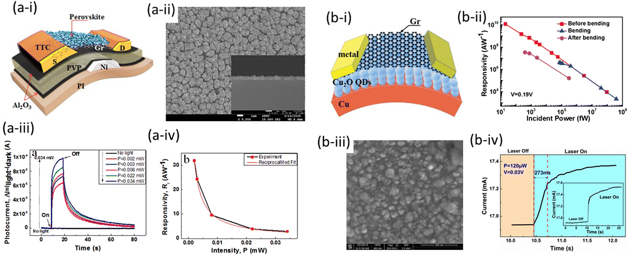 | ||
| Fig. 11 (a) Graphene/perovskite flexible PDs: (a-i) device schematic, (a-ii) a top-view SEM image, (a-iii) time-dependent photocurrent, and (a-iv) responsivity under different intensities at a 515 nm wavelength and 1 V source-drain voltage.185 Reproduced with permission from ref. 185. Copyright 2016, Elsevier Ltd. (b) Graphene/Cu2O quantum dots: (b-i) photodetector structure, (b-ii) responsivity vs. incident power under a 450 nm laser, (b-iii) a plan-view SEM image and (b-iv) temporal response.189 Reproduced with permission from ref. 189. Copyright 2019, Wiley-VCH. | ||
Like BP, graphene also has been applied in a wide range of electronic devices such as transistors and supercapacitors owing to its high specific capacitance, power density, stability, and fast charge–discharge rate compared to conventional energy storage devices (e.g. batteries and capacitors).36,197 However, we do not provide a review of the widely researched applications of Graphene in electronic devices in detail because our review focuses on flexible optoelectronic devices.
6. Conclusions
In summary, we have presented recent progress in NBG semiconductor NMs from their material preparation to applications in flexible optoelectronic devices, which is provided in Table 3. For the fabrication process, different approaches can be used depending on the materials; Ge, GeSn, and InGaAs NMs. They mainly use a semiconductor-on-insulator platform; meanwhile, 2D materials are typically based on exfoliation procedures. The material characteristics of NBG semiconductors are summarized in this review. We also cover the recent progressive results in their device applications such as flexible optical sensors, van der Waals heterojunction diodes, light emitting diodes, logical inverters, solar cells, etc. This broad range of device applications is possible due to their outstanding mechanical and optoelectronic properties, including superb flexibility, high carrier mobility, thin thickness, and easiness to apply strain. Furthermore, advanced techniques, which overcome the drawbacks of the NBG NMs, are reviewed such as strain engineering in GeSn and band-gap tuning of 2D materials by controlling layer thickness or doping. The development of high-performance flexible PDs using 2D materials has been limited because of their challengeable synthesis and fabrication methods, high surface defect density, and poor stability in air and water. For BP, the fabrication process and stability are the main challenges in flexible optoelectronic device applications. To overcome these challenges, the methods to synthesize large-area BP with large grain sizes and low defects should be studied. Also, passivation strategies to reduce surface defects should be investigated and the main causes of the device degradation under the air should be researched. About graphene, which has been studied much longer than BP in terms of its fabrication and applications, zero-bandgap has been one of the main challenges in fabricating heterojunction optoelectronic devices using graphene as a junction. Thus, in-depth studies on the strategies to control the graphene bandgap are required. Further improvement in its synthesis for large-area, low-defect, and highly stable materials and devices are still needed. In conclusion, the NBG NMs will bring exceptional advances in wearable devices or biomedical applications because of their unique material and device characteristics, which cannot be realized by bulk semiconductors.| Materials | Bias voltage (V) | Dark current | Dark current density | Wavelength (nm) | 3-dB (Hz) | Rise time (s) | Responsivity (A/W) | Ref. |
|---|---|---|---|---|---|---|---|---|
| Flexible Ge | 1 | — | 9.6 mA cm−2 | 1550 | — | 2.2 × 10⁻³ |
0.05 | 15 |
| Flexible GeSn | 2 | 8.1 μA | 0.09 A cm−2 | 2000 | — | — | 1.03 × 10⁻³ |
19 |
| Flexible GeSn | 2 | — | 28 mA cm−2 | 1550 | — | — | 0.148 | 65 |
| Flexible InGaAs | 5 | 170 pA | — | 1550 | 1.4× 10⁹ |
— | 0.35 | 88 |
| Flexible BP | 0.3 | −20 to −30 μA | — | 830 | — | — | 53 | 143 |
| Flexible BP | 0.1 | — | — | 1650 | 103 | 18.6 × 10⁻⁶ |
0.5–2.5 | 144 |
| Flexible Bi NSs-BP QD | 0 | — | 0.05 uA cm−2 | Vis light (Xe lamp) | — | 330 × 10−3 |
2.8 × 10⁻⁶ |
145 |
| Flexible graphene/perovskite | 1 | 4.1 mA | — | 515 | — | 3.2 | 115 | 185 |
| Flexible graphene/ZnO nanorod | 1 | 3.2 mA | — | 365 | — | — | 2.5 × 10⁶ | 186 |
| Flexible graphene/Cu3-xP NC | 1 | 20 uA | — | 405 | — | 0.42 | 1.59 × 10⁵ | 187 |
| Flexible graphene/NMe2-GQD | 0.1 | 1.3 mA | — | 255 | — | 3.7 | 1.5 × 10⁴ | 188 |
| Flexible graphene/CuO2 QD | 0.19 | 0.1 A | — | 450 | — | — | 1.2 × 10¹⁰ | 189 |
Conflicts of interest
There are no conflicts to declare.Acknowledgements
This work was supported by the A*STAR, Singapore, Advanced Manufacturing and Engineering (AME) Young Individual Research Grant (YIRG) and IRG under the Project A2084c0066 and M21K2c0107, respectively, and the Ministry of Education, Singapore, under the Grant ACRF Tier 2 grant (T2EP50120-0001). The authors acknowledge the support of the Nanyang NanoFabrication Centre (N2FC).References
- J. Tsao, S. Chowdhury, M. Hollis, D. Jena, N. Johnson, K. Jones, R. Kaplar, S. Rajan, C. Van de Walle and E. Bellotti, Adv. Electron. Mater., 2018, 4, 1600501 CrossRef.
- S. An, Y. Liao, S. Shin and M. Kim, Adv. Mater. Technol., 2021, 2100912 Search PubMed.
- S. Su, B. Cheng, C. Xue, W. Wang, Q. Cao, H. Xue, W. Hu, G. Zhang, Y. Zuo and Q. Wang, Opt. Express, 2011, 19, 6400–6405 CrossRef CAS PubMed.
- M. Piccardo, N. A. Rubin, L. Meadowcroft, P. Chevalier, H. Yuan, J. Kimchi and F. Capasso, Appl. Phys. Lett., 2018, 112, 041106 CrossRef.
- J. Zhang, M. A. Itzler, H. Zbinden and J.-W. Pan, Light: Sci. Appl., 2015, 4, e286–e286 CrossRef CAS.
- K. Wang, L. W. Yap, S. Gong, R. Wang, S. J. Wang and W. Cheng, Adv. Funct. Mater., 2021, 31, 2008347 CrossRef CAS.
- M. Sang, K. Kang, Y. Zhang, H. Zhang, K. Kim, M. Cho, J. Shin, J. H. Hong, T. Kim and S. K. Lee, Adv. Mater., 2022, 34, 2105865 CrossRef CAS PubMed.
- D. Yadav and D. R. Nair, IEEE J. Electron Devices Soc., 2020, 8, 308–315 CAS.
- Y. Yang, X. Wang, C. Wang, Y. Song, M. Zhang, Z. Xue, S. Wang, Z. Zhu, G. Liu and P. Li, Nano Lett., 2020, 20, 3872–3879 CrossRef CAS PubMed.
- I. Yang, Z. Li, J. Wong-Leung, Y. Zhu, Z. Li, N. Gagrani, L. Li, M. N. Lockrey, H. Nguyen and Y. Lu, Nano Lett., 2019, 19, 3821–3829 CrossRef CAS PubMed.
- K. Chiba, A. Yoshida, K. Tomioka and J. Motohisa, ACS Photonics, 2019, 6, 260–264 CrossRef CAS.
- J. Valente, T. Godde, Y. Zhang, D. J. Mowbray and H. Liu, Nano Lett., 2018, 18, 4206–4213 CrossRef CAS PubMed.
- Y.-C. Tai, P.-L. Yeh, S. An, H.-H. Cheng, M. Kim and G.-E. Chang, Nanotechnology, 2020, 31, 445301 CrossRef CAS PubMed.
- A. Zumeit, A. S. Dahiya, A. Christou, D. Shakthivel and R. Dahiya, npj Flexible Electron., 2021, 5, 1–10 CrossRef.
- S. An, S. Wu, K.-H. Lee, C. S. Tan, Y.-C. Tai, G.-E. Chang and M. Kim, ACS Appl. Electron. Mater., 2021, 1780–1786 CrossRef CAS.
- J. Greil, A. Lugstein, C. Zeiner, G. Strasser and E. Bertagnolli, Nano Lett., 2012, 12, 6230–6234 CrossRef CAS PubMed.
- J. Kim and M. V. Fischetti, J. Appl. Phys., 2010, 108, 013710 CrossRef.
- M. El Kurdi, G. Fishman, S. Sauvage and P. Boucaud, J. Appl. Phys., 2010, 107, 013710 CrossRef.
- S. An, S. Wu, C. S. Tan, G.-E. Chang, X. Gong and M. Kim, J. Mater. Chem. C, 2020, 8, 13557–13562 RSC.
- M. Kim, J.-H. Seo, Z. Yu, W. Zhou and Z. Ma, Appl. Phys. Lett., 2016, 109, 051105 CrossRef.
- Y. Y. Zhang, S. An, Y. Zheng, J. Lai, J. H. Seo, K. H. Lee and M. Kim, Appl. Electron. Mater., 2022, 8, 2100652 CAS.
- J.-H. Seo, E. Swinnich, Y.-Y. Zhang and M. Kim, Mater. Res. Lett., 2020, 8, 123–144 CrossRef CAS.
- J. Lai, M. N. Hasan, E. Swinnich, Z. Tang, S.-H. Shin, M. Kim, P. Zhang and J.-H. Seo, J. Mater. Chem. C, 2020, 8, 14732–14739 RSC.
- S. Mikael, J.-H. Seo, D.-W. Park, M. Kim, H. Mi, A. Javadi, S. Gong and Z. Ma, Extreme Mech. Lett., 2017, 11, 77–83 CrossRef.
- M. Kim, H. Mi, M. Cho, J.-H. Seo, W. Zhou, S. Gong and Z. Ma, Appl. Phys. Lett., 2015, 106, 212107 CrossRef.
- H.-C. Yuan, J. Shin, G. Qin, L. Sun, P. Bhattacharya, M. G. Lagally, G. K. Celler and Z. Ma, Appl. Phys. Lett., 2009, 94, 013102 CrossRef.
- D. Nam, D. Sukhdeo, S.-L. Cheng, A. Roy, K. Chih-Yao Huang, M. Brongersma, Y. Nishi and K. Saraswat, Appl. Phys. Lett., 2012, 100, 131112 CrossRef.
- Z. Xia, H. Song, M. Kim, M. Zhou, T. H. Chang, D. Liu, K. Xiong, Z. Yu, Z. Ma and Q. Gan, Photodetecting MOSFET based on ultrathin single-crystal germanium nanomembrane, 2016Conference on Lasers and Electro-Optics (CLEO), San Jose, CA, USA, 2016, pp. 1–2 Search PubMed.
- M. Kim, J. Park, W. Zhou and Z. Ma, Inorganic Flexible Optoelectronics, 2019, pp. 79–116 DOI:10.1002/9783527813001.ch3.
- Z. Xia, H. Song, M. Kim, M. Zhou, T.-H. Chang, D. Liu, X. Yin, K. Xiong, H. Mi, X. Wang, F. Xia, Z. Yu, Z. Ma and Q. Gan, Sci. Adv., 2017, 3, e1602783 CrossRef PubMed.
- M. Cho, J.-H. Seo, M. Kim, J. Lee, D. Liu, W. Zhou, Z. Yu and Z. Ma, J. Vac. Sci. Technol., B: Nanotechnol. Microelectron.: Mater., Process., Meas., Phenom., 2016, 34, 040604 Search PubMed.
- A. Gassenq, I. Duchemin, Y.-M. Niquet, A. Glière, N. Pauc, A. Chelnokov, V. Reboud and V. Calvo, IEEE Photonics J., 2021, 14, 1–4 Search PubMed.
- A. Gassenq, K. Guilloy, G. Osvaldo Dias, N. Pauc, D. Rouchon, J.-M. Hartmann, J. Widiez, S. Tardif, F. Rieutord and J. Escalante, Appl. Phys. Lett., 2015, 107, 191904 CrossRef.
- K. A. Madurani, S. Suprapto, N. I. Machrita, S. L. Bahar, W. Illiya and F. Kurniawan, ECS J. Solid State Sci. Technol., 2020, 9, 093013 CrossRef CAS.
- X. Peng and Y. Yan, J. Eur. Opt. Soc., 2021, 17, 16 CrossRef.
- A. Velasco, Y. K. Ryu, A. Boscá, A. Ladrón-de-Guevara, E. Hunt, J. Zuo, J. Pedrós, F. Calle and J. Martinez, Sustainable Energy Fuels, 2021, 5, 1235–1254 RSC.
- X. Chen, J. S. Ponraj, D. Fan and H. Zhang, Nanoscale, 2020, 12, 3513–3534 RSC.
- Y.-Y. Li, B. Gao, Y. Han, B.-K. Chen and J.-Y. Huo, Front. Phys., 2021, 16, 43301 CrossRef.
- V. Tran, R. Soklaski, Y. Liang and L. Yang, Phys. Rev. B: Condens. Matter Mater. Phys., 2014, 89, 235319 CrossRef.
- K. S. Novoselov, A. K. Geim, S. V. Morozov, D. Jiang, Y. Zhang, S. V. Dubonos, I. V. Grigorieva and A. A. Firsov, Science, 2004, 306, 666–669 CrossRef CAS PubMed.
- M. Poljak, V. Jovanovic, D. Grgec and T. Suligoj, IEEE Trans. Electron Devices, 2012, 59, 1636–1643 CAS.
- P. Kumar, B. S. Bhadoria, S. Kumar, S. Bhowmick, Y. S. Chauhan and A. Agarwal, Phys. Rev. B, 2016, 93, 195428 CrossRef.
- E. J. G. Santos and E. Kaxiras, Nano Lett., 2013, 13, 898–902 CrossRef CAS PubMed.
- D. Zhang, X. Hu, D. Liu, X. Lin, W. Wang, Z. Ding, Z. Wang, B. Cheng and C. Xue, 2018.
- Y. Chuang, C.-Y. Liu, G.-L. Luo and J.-Y. Li, IEEE Electron Device Lett., 2020, 42, 10–13 Search PubMed.
- L. Li, Y. Yu, G. J. Ye, Q. Ge, X. Ou, H. Wu, D. Feng, X. H. Chen and Y. Zhang, Nat. Nanotechnol., 2014, 9, 372–377 CrossRef CAS PubMed.
- V. E. Dorgan, M.-H. Bae and E. Pop, Appl. Phys. Lett., 2010, 97, 082112 CrossRef.
- K. Moto, N. Saitoh, N. Yoshizawa, T. Suemasu and K. Toko, Appl. Phys. Lett., 2019, 114, 112110 CrossRef.
- H. Liu, A. T. Neal, Z. Zhu, Z. Luo, X. Xu, D. Tománek and P. D. Ye, ACS Nano, 2014, 8, 4033–4041 CrossRef CAS PubMed.
- P. Maycock, Solid-State Electron., 1967, 10, 161–168 CrossRef CAS.
- Z. Luo, J. Maassen, Y. Deng, Y. Du, R. P. Garrelts, M. S. Lundstrom, P. D. Ye and X. Xu, Nat. Commun., 2015, 6, 8572 CrossRef CAS PubMed.
- A. A. Balandin, Nat. Mater., 2011, 10, 569–581 CrossRef CAS PubMed.
- X. Li, Z. Yu, X. Xiong, T. Li, T. Gao, R. Wang, R. Huang and Y. Wu, Sci. Adv., 2019, 5, eaau3194 CrossRef PubMed.
- S. Gupta, B. Magyari-Köpe, Y. Nishi and K. C. Saraswat, J. Appl. Phys., 2013, 113, 073707 CrossRef.
- S. Mellaerts, V. Afanas’ ev, J. W. Seo, M. Houssa and J.-P. Locquet, ACS Appl. Mater. Interfaces, 2021, 13, 30941–30949 CrossRef CAS PubMed.
- W. Dou, High-Sn-content GeSn Alloy towards Room-temperature Mid Infrared Laser, University of Arkansas, 2018 Search PubMed.
- M. R. Atalla, S. Assali, A. Attiaoui, C. Lemieux-Leduc, A. Kumar, S. Abdi and O. Moutanabbir, Adv. Funct. Mater., 2020, 2006329 Search PubMed.
- C. S. Fenrich, X. Chen, R. Chen, Y.-C. Huang, H. Chung, M.-Y. Kao, Y. Huo, T. I. Kamins and J. S. Harris, ACS Photonics, 2016, 3, 2231–2236 CrossRef CAS.
- X. Wu, Z. Tian, H. Cong, Y. Wang, R. Edy, G. Huang, Z. Di, C. Xue and Y. Mei, Nanotechnology, 2018, 29, 42LT02 CrossRef PubMed.
- R. Paiella and M. G. Lagally, Nanomaterials, 2018, 8, 407 CrossRef PubMed.
- A. Gok, X. Wang, S. Scott, A. Bhat, H. Yan, A. Pattammattel, E. Nazaretski, Y. S. Chu, Z. Huang, R. M. Osgood, M. G. Lagally and R. Paiella, ACS Appl. Nano Mater., 2021, 4, 6160–6169 CrossRef CAS.
- S. An, Y.-C. Tai, K.-C. Lee, S. Shin, H.-H. Cheng, G.-E. Chang and M. Kim, Nanotechnology, 2021, 355704 CrossRef CAS PubMed.
- M. R. M. Atalla, S. Assali, A. Attiaoui, C. Lemieux-Leduc, A. Kumar, S. Abdi and O. Moutanabbir, Adv. Funct. Mater., 2021, 31, 2006329 CrossRef CAS.
- F. Yasar, W. Fan and Z. Ma, IEEE Photonics J., 2018, 10, 1–9 Search PubMed.
- S. An, Y. Liao and M. Kim, ACS Appl. Mater. Interfaces, 2021, 13, 61396–61403 CrossRef CAS PubMed.
- R. Chen, S. Gupta, Y.-C. Huang, Y. Huo, C. W. Rudy, E. Sanchez, Y. Kim, T. I. Kamins, K. C. Saraswat and J. S. Harris, Nano Lett., 2014, 14, 37–43 CrossRef CAS PubMed.
- R. Millar, D. Dumas, K. Gallacher, P. Jahandar, C. MacGregor, M. Myronov and D. Paul, Opt. Express, 2017, 25, 25374–25385 CrossRef CAS PubMed.
- V. Reboud, A. Gassenq, N. Pauc, J. Aubin, L. Milord, Q. Thai, M. Bertrand, K. Guilloy, D. Rouchon and J. Rothman, Appl. Phys. Lett., 2017, 111, 092101 CrossRef.
- Q. M. Thai, N. Pauc, J. Aubin, M. Bertrand, J. Chrétien, V. Delaye, A. Chelnokov, J.-M. Hartmann, V. Reboud and V. Calvo, Opt. Express, 2018, 26, 32500–32508 CrossRef CAS PubMed.
- Q. Thai, N. Pauc, J. Aubin, M. Bertrand, J. Chrétien, A. Chelnokov, J. Hartmann, V. Reboud and V. Calvo, Appl. Phys. Lett., 2018, 113, 051104 CrossRef.
- J. Yin, X. Cui, X. Wang, P. Sookchoo, M. G. Lagally and R. Paiella, Appl. Phys. Lett., 2016, 108, 241107 CrossRef.
- A. Elbaz, D. Buca, N. von den Driesch, K. Pantzas, G. Patriarche, N. Zerounian, E. Herth, X. Checoury, S. Sauvage and I. Sagnes, Nat. Photonics, 2020, 14, 375–382 CrossRef CAS.
- A. Elbaz, R. Arefin, E. Sakat, B. Wang, E. Herth, G. Patriarche, A. Foti, R. Ossikovski, S. Sauvage and X. Checoury, ACS Photonics, 2020, 7, 2713–2722 CrossRef CAS.
- W. Li, P. Anantha, S. Bao, K. H. Lee, X. Guo, T. Hu, L. Zhang, H. Wang, R. Soref and C. S. Tan, Appl. Phys. Lett., 2016, 109, 241101 CrossRef.
- S. Kim, J.-H. Han, J.-P. Shim, H.-j Kim and W. J. Choi, Opt. Mater. Express, 2018, 8, 440–451 CrossRef CAS.
- J. Ma, Z. Zhang, G. Miao and Y. Zhao, Jpn. J. Appl. Phys., 2015, 54, 104301 CrossRef.
- D.-S. Um, S. Lim, Y. Lee, H. Lee, H.-J. Kim, W.-C. Yen, Y.-L. Chueh and H. Ko, ACS Nano, 2014, 8, 3080–3087 CrossRef CAS PubMed.
- H. Kim, C. S. Chang, S. Lee, J. Jiang, J. Jeong, M. Park, Y. Meng, J. Ji, Y. Kwon and X. Sun, Nat. Rev. Methods Primers, 2022, 2, 1–21 CrossRef.
- H. Kim, K. Lu, Y. Liu, H. S. Kum, K. S. Kim, K. Qiao, S.-H. Bae, S. Lee, Y. J. Ji and K. H. Kim, ACS Nano, 2021, 15, 10587–10596 CrossRef CAS PubMed.
- Y. Kim, S. S. Cruz, K. Lee, B. O. Alawode, C. Choi, Y. Song, J. M. Johnson, C. Heidelberger, W. Kong and S. Choi, Nature, 2017, 544, 340–343 CrossRef CAS PubMed.
- W. Kong, H. Li, K. Qiao, Y. Kim, K. Lee, Y. Nie, D. Lee, T. Osadchy, R. J. Molnar and D. K. Gaskill, Nat. Mater., 2018, 17, 999–1004 CrossRef CAS PubMed.
- H. Kim, J. C. Kim, Y. Jeong, J. Yu, K. Lu, D. Lee, N. Kim, H. Y. Jeong, J. Kim and S. Kim, J. Appl. Phys., 2021, 130, 174901 CrossRef CAS.
- Y. Li, A. Alian, M. Sivan, L. Huang, K. W. Ang, D. Lin, D. Mocuta, N. Collaert and A. V.-Y. Thean, APL Mater., 2019, 7, 031503 CrossRef.
- W. Chen, T. Alford, T. Kuech and S. Lau, Appl. Phys. Lett., 2011, 98, 203509 CrossRef.
- X. Wang, X. Cui, A. Bhat, D. E. Savage, J. L. Reno, M. G. Lagally and R. Paiella, Appl. Phys. Lett., 2018, 113, 201105 CrossRef.
- S. M. Harazim, P. Feng, S. Sanchez, C. Deneke, Y. Mei and O. G. Schmidt, Nanoscale Res. Lett., 2011, 6, 1–8 CrossRef PubMed.
- D. Fan, K. Lee and S. R. Forrest, ACS Photonics, 2016, 3, 670–676 CrossRef CAS.
- L. Li, H. Lin, Y. Huang, R.-J. Shiue, A. Yadav, J. Li, J. Michon, D. Englund, K. Richardson and T. Gu, Optica, 2018, 5, 44–51 CrossRef.
- J. Shi, N. Wichmann, Y. Roelens and S. Bollaert, Appl. Phys. Lett., 2013, 102, 243503 CrossRef.
- Z. Yan, Y. Han, L. Lin, Y. Xue, C. Ma, W. K. Ng, K. S. Wong and K. M. Lau, Light: Sci. Appl., 2021, 10, 1–10 CrossRef PubMed.
- D.-S. Um, Y. Lee, S. Lim, J. Park, W.-C. Yen, Y.-L. Chueh, H.-J. Kim and H. Ko, ACS Appl. Mater. Interfaces, 2016, 8, 26105–26111 CrossRef CAS PubMed.
- S. An, Y. C. Huang, C. Y. Wu, P. R. Huang, G. E. Chang, J. Lai, J. H. Seo and M. Kim, Adv. Mater. Technol., 2022, 2201136 CrossRef.
- Y. Lee, D.-S. Um, S. Lim, H. Lee, M. P. Kim, T.-Y. Yang, Y.-L. Chueh, H.-J. Kim and H. Ko, ACS Appl. Mater. Interfaces, 2019, 11, 23382–23391 CrossRef CAS PubMed.
- Y. Du, C. Ouyang, S. Shi and M. Lei, J. Appl. Phys., 2010, 107, 093718 CrossRef.
- A. N. Rudenko and M. I. Katsnelson, Phys. Rev. B: Condens. Matter Mater. Phys., 2014, 89, 201408 CrossRef.
- P. W. Bridgman, J. Am. Chem. Soc., 1914, 36, 1344–1363 CrossRef CAS.
- I. Shirotani, Mol. Cryst. Liq. Cryst., 1982, 86, 203–211 CrossRef.
- C. Li, Y. Wu, B. Deng, Y. Xie, Q. Guo, S. Yuan, X. Chen, M. Bhuiyan, Z. Wu, K. Watanabe, T. Taniguchi, H. Wang, J. J. Cha, M. Snure, Y. Fei and F. Xia, Adv. Mater., 2018, 30, 1703748 CrossRef PubMed.
- C.-M. Park and H.-J. Sohn, Adv. Mater., 2007, 19, 2465–2468 CrossRef CAS.
- H. Krebs, H. Weitz and K. H. Worms, Z. Anorg. Allg. Chem., 1955, 280, 119–133 CrossRef CAS.
- A. Brown and S. Rundqvist, Acta Crystallogr., 1965, 19, 684–685 CrossRef CAS.
- Y. Maruyama, S. Suzuki, K. Kobayashi and S. Tanuma, Physica B + C, 1981, 105, 99–102 CrossRef CAS.
- M. Köpf, N. Eckstein, D. Pfister, C. Grotz, I. Krüger, M. Greiwe, T. Hansen, H. Kohlmann and T. Nilges, J. Cryst. Grow., 2014, 405, 6–10 CrossRef.
- S. Lange, P. Schmidt and T. Nilges, Inorg. Chem., 2007, 46, 4028–4035 CrossRef CAS PubMed.
- Y. Yi, X.-F. Yu, W. Zhou, J. Wang and P. K. Chu, Mater. Sci. Eng., R, 2017, 120, 1–33 CrossRef.
- N. Sultana, A. Degg, S. Upadhyaya, T. Nilges and N. Sen Sarma, Mater. Adv., 2022, 3, 5557–5574 RSC.
- Y. Zeng and Z. Guo, iScience, 2021, 24, 103116 CrossRef CAS PubMed.
- W. Lu, H. Nan, J. Hong, Y. Chen, C. Zhu, Z. Liang, X. Ma, Z. Ni, C. Jin and Z. Zhang, Nano Res., 2014, 7, 853–859 CrossRef CAS.
- J. Pei, X. Gai, J. Yang, X. Wang, Z. Yu, D.-Y. Choi, B. Luther-Davies and Y. Lu, Nat. Commun., 2016, 7, 10450 CrossRef CAS PubMed.
- J. R. Brent, N. Savjani, E. A. Lewis, S. J. Haigh, D. J. Lewis and P. O'Brien, Chem. Commun., 2014, 50, 13338–13341 RSC.
- A. H. Woomer, T. W. Farnsworth, J. Hu, R. A. Wells, C. L. Donley and S. C. Warren, ACS Nano, 2015, 9, 8869–8884 CrossRef CAS PubMed.
- P. Yasaei, B. Kumar, T. Foroozan, C. Wang, M. Asadi, D. Tuschel, J. E. Indacochea, R. F. Klie and A. Salehi-Khojin, Adv. Mater., 2015, 27, 1887–1892 CrossRef CAS PubMed.
- D. Hanlon, C. Backes, E. Doherty, C. S. Cucinotta, N. C. Berner, C. Boland, K. Lee, A. Harvey, P. Lynch, Z. Gholamvand, S. Zhang, K. Wang, G. Moynihan, A. Pokle, Q. M. Ramasse, N. McEvoy, W. J. Blau, J. Wang, G. Abellan, F. Hauke, A. Hirsch, S. Sanvito, D. D. O’Regan, G. S. Duesberg, V. Nicolosi and J. N. Coleman, Nat. Commun., 2015, 6, 8563 CrossRef CAS PubMed.
- W. Chen, K. Li, Y. Wang, X. Feng, Z. Liao, Q. Su, X. Lin and Z. He, J. Phys. Chem. Lett., 2017, 8, 591–598 CrossRef CAS PubMed.
- K. Chen, Y. Wang, J. Liu, J. Kang, Y. Ge, W. Huang, Z. Lin, Z. Guo, Y. Zhang and H. Zhang, Nanoscale, 2019, 11, 16852–16859 RSC.
- H. U. Lee, S. Y. Park, S. C. Lee, S. Choi, S. Seo, H. Kim, J. Won, K. Choi, K. S. Kang, H. G. Park, H.-S. Kim, H. R. An, K.-H. Jeong, Y.-C. Lee and J. Lee, Small, 2016, 12, 214–219 CrossRef CAS PubMed.
- W. Zhao, Z. Xue, J. Wang, J. Jiang, X. Zhao and T. Mu, ACS Appl. Mater. Interfaces, 2015, 7, 27608–27612 CrossRef CAS PubMed.
- B. Tian, B. Tian, B. Smith, M. C. Scott, Q. Lei, R. Hua, Y. Tian and Y. Liu, Proc. Natl. Acad. Sci. U. S. A., 2018, 115, 4345–4350 CrossRef CAS PubMed.
- M. B. Erande, S. R. Suryawanshi, M. A. More and D. J. Late, Eur. J. Inorg. Chem., 2015, 3102–3107 CrossRef CAS.
- A. Ambrosi, Z. Sofer and M. Pumera, Angew. Chem., Int. Ed., 2017, 56, 10443–10445 CrossRef CAS PubMed.
- X. Tang, W. Liang, J. Zhao, Z. Li, M. Qiu, T. Fan, C. S. Luo, Y. Zhou, Y. Li, Z. Guo, D. Fan and H. Zhang, Small, 2017, 13, 1702739 CrossRef PubMed.
- Y. Wang, F. Zhang, X. Tang, X. Chen, Y. Chen, W. Huang, Z. Liang, L. Wu, Y. Ge, Y. Song, J. Liu, D. Zhang, J. Li and H. Zhang, Laser Photonics Rev., 2018, 12, 1800016 CrossRef.
- Z. Huang, H. Hou, Y. Zhang, C. Wang, X. Qiu and X. Ji, Adv. Mater., 2017, 29, 1702372 CrossRef PubMed.
- J. Li, C. Chen, S. Liu, J. Lu, W. P. Goh, H. Fang, Z. Qiu, B. Tian, Z. Chen, C. Yao, W. Liu, H. Yan, Y. Yu, D. Wang, Y. Wang, M. Lin, C. Su and J. Lu, Chem. Mater., 2018, 30, 2742–2749 CrossRef CAS.
- S. Yang, K. Zhang, A. G. Ricciardulli, P. Zhang, Z. Liao, M. R. Lohe, E. Zschech, P. W. M. Blom, W. Pisula, K. Müllen and X. Feng, Angew. Chem., Int. Ed., 2018, 57, 4677–4681 CrossRef CAS PubMed.
- L. Zu, X. Gao, H. Lian, C. Li, Q. Liang, Y. Liang, X. Cui, Y. Liu, X. Wang and X. Cui, J. Alloys Compd., 2019, 770, 26–34 CrossRef CAS.
- C. C. Mayorga-Martinez, N. Mohamad Latiff, A. Y. S. Eng, Z. Sofer and M. Pumera, Anal. Chem., 2016, 88, 10074–10079 CrossRef CAS PubMed.
- A. Rabiei Baboukani, I. Khakpour, V. Drozd, A. Allagui and C. Wang, J. Mater. Chem. A, 2019, 7, 25548–25556 RSC.
- J. B. Smith, D. Hagaman and H.-F. Ji, Nanotechnology, 2016, 27, 215602 CrossRef PubMed.
- Z. Yang, J. Hao, S. Yuan, S. Lin, H. M. Yau, J. Dai and S. P. Lau, Adv. Mater., 2015, 27, 3748–3754 CrossRef CAS PubMed.
- Z. Wu, Y. Lyu, Y. Zhang, R. Ding, B. Zheng, Z. Yang, S. P. Lau, X. H. Chen and J. Hao, Nat. Mater., 2021, 20, 1203–1209 CrossRef CAS PubMed.
- Y. Xu, J. Yuan, L. Fei, X. Wang, Q. Bao, Y. Wang, K. Zhang and Y. Zhang, Small, 2016, 12, 5000–5007 CrossRef CAS PubMed.
- Y. Zhang, X. Rui, Y. Tang, Y. Liu, J. Wei, S. Chen, W. R. Leow, W. Li, Y. Liu, J. Deng, B. Ma, Q. Yan and X. Chen, Adv. Energy Mater., 2016, 6, 1502409 CrossRef.
- J. Na, Y. T. Lee, J. A. Lim, D. K. Hwang, G.-T. Kim, W. K. Choi and Y.-W. Song, ACS Nano, 2014, 8, 11753–11762 CrossRef CAS PubMed.
- B. Wan, B. Yang, Y. Wang, J. Zhang, Z. Zeng, Z. Liu and W. Wang, Nanotechnology, 2015, 26, 435702 CrossRef PubMed.
- H. Uk Lee, S. C. Lee, J. Won, B.-C. Son, S. Choi, Y. Kim, S. Y. Park, H.-S. Kim, Y.-C. Lee and J. Lee, Sci. Rep., 2015, 5, 8691 CrossRef PubMed.
- R. A. Doganov, E. C. T. O’Farrell, S. P. Koenig, Y. Yeo, A. Ziletti, A. Carvalho, D. K. Campbell, D. F. Coker, K. Watanabe, T. Taniguchi, A. H. C. Neto and B. Özyilmaz, Nat. Commun., 2015, 6, 6647 CrossRef CAS PubMed.
- C. R. Ryder, J. D. Wood, S. A. Wells, Y. Yang, D. Jariwala, T. J. Marks, G. C. Schatz and M. C. Hersam, Nat. Chem., 2016, 8, 597–602 CrossRef CAS PubMed.
- W. Gu, X. Pei, Y. Cheng, C. Zhang, J. Zhang, Y. Yan, C. Ding and Y. Xian, ACS Sens., 2017, 2, 576–582 CrossRef CAS PubMed.
- D. Tofan, Y. Sakazaki, K. L. Walz Mitra, R. Peng, S. Lee, M. Li and A. Velian, Angew. Chem., Int. Ed., 2021, 60, 8329–8336 CrossRef CAS PubMed.
- Q. Wei and X. Peng, Appl. Phys. Lett., 2014, 104, 251915 CrossRef.
- W. Zhu, M. N. Yogeesh, S. Yang, S. H. Aldave, J.-S. Kim, S. Sonde, L. Tao, N. Lu and D. Akinwande, Nano Lett., 2015, 15, 1883–1890 CrossRef CAS PubMed.
- J. Miao, B. Song, Q. Li, L. Cai, S. Zhang, W. Hu, L. Dong and C. Wang, ACS Nano, 2017, 11, 6048–6056 CrossRef CAS PubMed.
- H. Kim, S. Z. Uddin, D.-H. Lien, M. Yeh, N. S. Azar, S. Balendhran, T. Kim, N. Gupta, Y. Rho, C. P. Grigoropoulos, K. B. Crozier and A. Javey, Nature, 2021, 596, 232–237 CrossRef CAS PubMed.
- Y. Zhou, H. Qiao, Z. Huang, Q. Ma, F. Liu, G. Liao, S. Luo, J. Zhong and X. Qi, ACS Sustainable Chem. Eng., 2021, 9, 14918–14926 CrossRef CAS.
- Y. Zhang, S. Wang, S. Chen, Q. Zhang, X. Wang, X. Zhu, X. Zhang, X. Xu, T. Yang, M. He, X. Yang, Z. Li, X. Chen, M. Wu, Y. Lu, R. Ma, W. Lu and A. Pan, Adv. Mater., 2020, 32, 1808319 CrossRef CAS PubMed.
- X. Zong, H. Hu, G. Ouyang, J. Wang, R. Shi, L. Zhang, Q. Zeng, C. Zhu, S. Chen, C. Cheng, B. Wang, H. Zhang, Z. Liu, W. Huang, T. Wang, L. Wang and X. Chen, Light: Sci. Appl., 2020, 9, 114 CrossRef CAS PubMed.
- J. Wang, A. Rousseau, M. Yang, T. Low, S. Francoeur and S. Kéna-Cohen, Nano Lett., 2020, 20, 3651–3655 CrossRef CAS PubMed.
- A. Pon, A. Bhattacharyya and R. Rathinam, J. Electron. Mater., 2021, 50, 6020–6036 CrossRef CAS.
- X. Du, I. Skachko, A. Barker and E. Y. Andrei, Nat. Nanotechnol., 2008, 3, 491–495 CrossRef CAS PubMed.
- A. A. Balandin, S. Ghosh, W. Bao, I. Calizo, D. Teweldebrhan, F. Miao and C. N. Lau, Nano Lett., 2008, 8, 902–907 CrossRef CAS PubMed.
- R. R. Nair, P. Blake, A. N. Grigorenko, K. S. Novoselov, T. J. Booth, T. Stauber, N. M. R. Peres and A. K. Geim, Science, 2008, 320, 1308 CrossRef CAS PubMed.
- C. Lee, X. Wei, J. W. Kysar and J. Hone, Science, 2008, 321, 385–388 CrossRef CAS PubMed.
- K. S. Novoselov, V. I. Fal′ko, L. Colombo, P. R. Gellert, M. G. Schwab and K. Kim, Nature, 2012, 490, 192–200 CrossRef CAS PubMed.
- F. Bonaccorso, A. Lombardo, T. Hasan, Z. Sun, L. Colombo and A. C. Ferrari, Mater. Today, 2012, 15, 564–589 CrossRef CAS.
- A. H. Castro Neto, F. Guinea, N. M. R. Peres, K. S. Novoselov and A. K. Geim, Rev. Mod. Phys., 2009, 81, 109–162 CrossRef CAS.
- B. C. Brodie, Philos. Trans. R. Soc. London, 1859, 149, 249–259 CrossRef.
- L. Staudenmaier, Ber. Dtsch. Chem. Ges., 1898, 31, 1481–1487 CrossRef CAS.
- D. Li, M. B. Müller, S. Gilje, R. B. Kaner and G. G. Wallace, Nat. Nanotechnol., 2008, 3, 101–105 CrossRef CAS PubMed.
- Y. Hernandez, V. Nicolosi, M. Lotya, F. M. Blighe, Z. Sun, S. De, I. T. McGovern, B. Holland, M. Byrne, Y. K. Gun'Ko, J. J. Boland, P. Niraj, G. Duesberg, S. Krishnamurthy, R. Goodhue, J. Hutchison, V. Scardaci, A. C. Ferrari and J. N. Coleman, Nat. Nanotechnol., 2008, 3, 563–568 CrossRef CAS PubMed.
- Y. Xu, H. Cao, Y. Xue, B. Li and W. Cai, Nanomaterials, 2018, 8, 942 CrossRef PubMed.
- Y. Hernandez, M. Lotya, D. Rickard, S. D. Bergin and J. N. Coleman, Langmuir, 2010, 26, 3208–3213 CrossRef CAS PubMed.
- X. Chen, J. F. Dobson and C. L. Raston, Chem. Commun., 2012, 48, 3703–3705 RSC.
- K. R. Paton, E. Varrla, C. Backes, R. J. Smith, U. Khan, A. O’Neill, C. Boland, M. Lotya, O. M. Istrate, P. King, T. Higgins, S. Barwich, P. May, P. Puczkarski, I. Ahmed, M. Moebius, H. Pettersson, E. Long, J. Coelho, S. E. O’Brien, E. K. McGuire, B. M. Sanchez, G. S. Duesberg, N. McEvoy, T. J. Pennycook, C. Downing, A. Crossley, V. Nicolosi and J. N. Coleman, Nat. Mater., 2014, 13, 624–630 CrossRef CAS PubMed.
- W. S. Hummers and R. E. Offeman, J. Am. Chem. Soc., 1958, 80, 1339 CrossRef CAS.
- K. Parvez, R. Li, S. R. Puniredd, Y. Hernandez, F. Hinkel, S. Wang, X. Feng and K. Müllen, ACS Nano, 2013, 7, 3598–3606 CrossRef CAS PubMed.
- A. J. Cooper, N. R. Wilson, I. A. Kinloch and R. A. W. Dryfe, Carbon, 2014, 66, 340–350 CrossRef CAS.
- J. Lin, Z. Peng, Y. Liu, F. Ruiz-Zepeda, R. Ye, E. L. G. Samuel, M. J. Yacaman, B. I. Yakobson and J. M. Tour, Nat. Commun., 2014, 5, 5714 CrossRef CAS PubMed.
- R. Ye, D. K. James and J. M. Tour, Acc. Chem. Res., 2018, 51, 1609–1620 CrossRef CAS PubMed.
- A. F. Carvalho, A. J. S. Fernandes, R. Martins, E. Fortunato and F. M. Costa, Adv. Mater. Technol., 2020, 5, 2000630 CrossRef CAS.
- B. Kulyk, B. F. R. Silva, A. F. Carvalho, S. Silvestre, A. J. S. Fernandes, R. Martins, E. Fortunato and F. M. Costa, ACS Appl. Mater. Interfaces, 2021, 13, 10210–10221 CrossRef CAS PubMed.
- A. F. Carvalho, A. J. S. Fernandes, C. Leitão, J. Deuermeier, A. C. Marques, R. Martins, E. Fortunato and F. M. Costa, Adv. Funct. Mater., 2018, 28, 1805271 CrossRef.
- Z. Zhang, M. Song, J. Hao, K. Wu, C. Li and C. Hu, Carbon, 2018, 127, 287–296 CrossRef CAS.
- Q. Yu, J. Lian, S. Siriponglert, H. Li, Y. P. Chen and S.-S. Pei, Appl. Phys. Lett., 2008, 93, 113103 CrossRef.
- K. S. Kim, Y. Zhao, H. Jang, S. Y. Lee, J. M. Kim, K. S. Kim, J.-H. Ahn, P. Kim, J.-Y. Choi and B. H. Hong, Nature, 2009, 457, 706–710 CrossRef CAS PubMed.
- X. Li, W. Cai, J. An, S. Kim, J. Nah, D. Yang, R. Piner, A. Velamakanni, I. Jung, E. Tutuc, S. K. Banerjee, L. Colombo and R. S. Ruoff, Science, 2009, 324, 1312–1314 CrossRef CAS PubMed.
- S.-Y. Kwon, C. V. Ciobanu, V. Petrova, V. B. Shenoy, J. Bareño, V. Gambin, I. Petrov and S. Kodambaka, Nano Lett., 2009, 9, 3985–3990 CrossRef CAS PubMed.
- B. J. Kang, J. H. Mun, C. Y. Hwang and B. J. Cho, J. Appl. Phys., 2009, 106, 104309 CrossRef.
- J. Coraux, A. T. N‘Diaye, C. Busse and T. Michely, Nano Lett., 2008, 8, 565–570 CrossRef CAS PubMed.
- C. Berger, Z. Song, X. Li, X. Wu, N. Brown, C. Naud, D. Mayou, T. Li, J. Hass, A. N. Marchenkov, E. H. Conrad, P. N. First and W. A. D. Heer, Science, 2006, 312, 1191–1196 CrossRef CAS PubMed.
- S. Y. Zhou, G. H. Gweon, A. V. Fedorov, P. N. First, W. A. de Heer, D. H. Lee, F. Guinea, A. H. Castro Neto and A. Lanzara, Nat. Mater., 2007, 6, 770–775 CrossRef CAS PubMed.
- G. Giovannetti, P. A. Khomyakov, G. Brocks, P. J. Kelly and J. van den Brink, Phys. Rev. B: Condens. Matter Mater. Phys., 2007, 76, 073103 CrossRef.
- Z. Fang, Z. Liu, Y. Wang, P. M. Ajayan, P. Nordlander and N. J. Halas, Nano Lett., 2012, 12, 3808–3813 CrossRef CAS PubMed.
- M. Freitag, T. Low, W. Zhu, H. Yan, F. Xia and P. Avouris, Nat. Commun., 2013, 4, 1951 CrossRef PubMed.
- V. Q. Dang, G.-S. Han, T. Q. Trung, L. T. Duy, Y.-U. Jin, B.-U. Hwang, H.-S. Jung and N.-E. Lee, Carbon, 2016, 105, 353–361 CrossRef CAS.
- V. Q. Dang, T. Q. Trung, L. T. Duy, B.-Y. Kim, S. Siddiqui, W. Lee and N.-E. Lee, ACS Appl. Mater. Interfaces, 2015, 7, 11032–11040 CrossRef CAS PubMed.
- T. Sun, Y. Wang, W. Yu, Y. Wang, Z. Dai, Z. Liu, B. N. Shivananju, Y. Zhang, K. Fu, B. Shabbir, W. Ma, S. Li and Q. Bao, Small, 2017, 13, 1701881 CrossRef PubMed.
- H. Tetsuka, Sci. Rep., 2017, 7, 5544 CrossRef PubMed.
- Q. Liu, H. Tian, J. Li, A. Hu, X. He, M. Sui and X. Guo, Adv. Opt. Mater., 2019, 7, 1900455 CrossRef CAS.
- S. Liu, Z. Huang, H. Qiao, R. Hu, Q. Ma, K. Huang, H. Li and X. Qi, Nanoscale Adv., 2020, 2, 906–912 RSC.
- J. M. Kim, S. Kim and S.-H. Choi, ACS Sustainable Chem. Eng., 2019, 7, 734–739 CrossRef CAS.
- P. Han, L. St Marie, Q. X. Wang, N. Quirk, A. El Fatimy, M. Ishigami and P. Barbara, Nanotechnology, 2018, 29, 20LT01 CrossRef PubMed.
- B. Fu, Y. Hua, X. Xiao, H. Zhu, Z. Sun and C. Yang, IEEE J. Sel. Top. Quantum Electron., 2014, 20, 411–415 Search PubMed.
- A. A. Lagatsky, Z. Sun, T. S. Kulmala, R. S. Sundaram, S. Milana, F. Torrisi, O. L. Antipov, Y. Lee, J. H. Ahn, C. T. A. Brown, W. Sibbett and A. C. Ferrari, Appl. Phys. Lett., 2013, 102, 013113 CrossRef.
- J. Ma, G. Q. Xie, P. Lv, W. L. Gao, P. Yuan, L. J. Qian, H. H. Yu, H. J. Zhang, J. Y. Wang and D. Y. Tang, Opt. Lett., 2012, 37, 2085–2087 CrossRef CAS PubMed.
- R. Mary, G. Brown, S. J. Beecher, F. Torrisi, S. Milana, D. Popa, T. Hasan, Z. Sun, E. Lidorikis, S. Ohara, A. C. Ferrari and A. K. Kar, Opt. Express, 2013, 21, 7943–7950 CrossRef CAS PubMed.
- Q. Ke and J. Wang, J. Materiomics, 2016, 2, 37–54 CrossRef.
Footnote |
| † These authors contributed equally |
| This journal is © The Royal Society of Chemistry 2023 |