
 Open Access Article
 This Open Access Article is licensed under a
 Creative Commons Attribution 3.0 Unported Licence
Environment effects upon electrodeposition of thin film copper oxide nanomaterials†
Mark A.
Buckingham
 *a,
Weichen
Xiao
a,
Brendan
Ward-O’Brien
a,
Kathryn
Yearsley
b,
Usama
Zulfiqar
a,
Ben
F. Spencer
a,
Allan
Matthews
*a and
David J.
Lewis
*a
*a,
Weichen
Xiao
a,
Brendan
Ward-O’Brien
a,
Kathryn
Yearsley
b,
Usama
Zulfiqar
a,
Ben
F. Spencer
a,
Allan
Matthews
*a and
David J.
Lewis
*a
aDepartment of Materials, The University of Manchester, Sackville Street, M13 9PL, UK. E-mail: mark.buckingham@manchester.ac.uk; allan.matthews@manchester.ac.uk; david.lewis-4@manchester.ac.uk
bApplied Sciences, BP Innovation and Engineering, BP plc, Saltend, Hull, HU12 8DS, UK
First published on 20th March 2023
Abstract
Copper(I) oxide (Cu2O) nanomaterials have become highly promising for photoelectrochemical reactions as both solar absorber layers in p–n heterojunction solar cells, direct photoelectrocatalysis and as electrodes in the CO2 reduction reaction. Here we undertake a synthetic study towards the synthesis of Cu2O nanocubes by utilising electrodeposition from copper salts (chloride, acetate, nitrate, and sulphate) in different solution environments. We initially set out to investigate the effect of electrolyte concentration on the growth of Cu2O nanocubes. We also set out to mimic the high resistance inherent in the low electrolyte concentration environment by altering the distance between the electrodes. This deposition method was found to enable control of nanocube size formation. Both mixed anion environments and mono-anion environments were also investigated in a low-electrolyte concentration system. The fundamental physiochemical and electrochemical properties of each solution such as pH, conductivity, open circuit potential (VOCP), solution resistance (RS), and electron transfer resistance (RET) were measured. We then deposited copper oxide nanomaterials as thin films on ITO-coated glass substrates and assessed the electrical (conductivity) and optical (UV-Vis and Eg) properties of these films. Finally, we set out to investigate if any possible correlations could be drawn between the physiochemical and electrochemical properties of the solution and the electronic and optical properties of the deposited Cu2O thin films.
Introduction
Copper oxide nanomaterials are highly desirable due to the earth abundant nature of Cu, low toxicity of the material and the direct, p-type band gap energy (Eg) between 1.7–2.2 eV, with high absorption coefficient (∼105 cm−1),1 which is commensurate with visible light photon absorption.2 The ability to tailor the growth plane and therefore morphology of copper oxide nanomaterials is also favourable for electro- and photo-catalytic reactions3,4 and for optoelectronic5–7 applications such as heterojunction solar cells.6,8 Copper oxide nanomaterials have also been extensively investigated for the CO2 reduction reaction (CO2RR),3,9–15 as copper-oxide is currently the only reported electrode surface to enable C2+ products.12,16 This is due to the unique electrocatalytic ability of Cu with an affinity to *CO strong enough to enable C–C bond formation, whilst not being too strong to be poisoned by intermediate CO absorption, which enable C–C formation towards hydrocarbon and alcohol products.17,18 Cu is also relatively weak at the competitive H+ reduction reaction compared to other transition metals such as Pt, Fe, and Ni.19 Other main group and transition metals such as Pb, Hg, Tl, and In, are selective towards formate production, with relatively little H2 and no other hydrocarbon products.19Synthesis of copper oxide nanomaterials have been reported using several methods.20 Solution phase (chemical) reduction,21,22 high pressure treatment,23 γ-irradiation,24 and solvothermal synthesis25 are techniques that have been demonstrated for copper oxide nanomaterial synthesis, however these techniques have limited control, especially at the atomic level and are unfavourable. These synthetic methods are also problematic because purification and deposition steps are required to generate thin film materials for example as electrodes or heterojunction solar cells. However, one method with high levels of control towards direct deposition to thin film nanomaterial electrodes is through electrochemical deposition.12
The issue with this technique is the wide range of conditions, techniques, and reported requirements for controlled growth. For example, seminal work investigating the shape-control of microscale copper oxide by Siegfried and Choi utilised surfactants to tailor the shape of electrodeposited copper oxide particles on ITO.26–28 In these reports they initially use a high temperature (60 °C), cathodic deposition under acidic conditions (pH 3.3–4.9) from the Cu(NO3)2 salt in the presence of Sodium dodecyl sulfate (SDS). In this work it was found that the ability of SDS to tailor the shape of copper oxide materials was highly dependent on the pH. With 5 wt% SDS at pH 3.9, truncated octahedra were observed, whereas at pH 3.7 cuboctahedra, pH 3.5 truncated cubes and at pH 3.4 cubes were observed.28 Further work by the same authors found that complex shapes could be obtained by electrodeposition in several mixed media, designed to favour different growth planes.27 The authors followed this work by continuing galvanostatic deposition of pre-grown cubic and octahedra Cu2O materials with random orientations in various media (NaNO3, [NH4]NO3, Na2SO4, [NH4]2SO4). The presence of [NH4]+ cations (i.e. acidic conditions in the absence of SDS) was found to form rhombicuboctahedral morphologies where both {110} and {111} planes develop simultaneously. NaNO3 was found to favour {100} plane growth (maintaining cubic shape) and the Na2SO4 system was found to develop {111} planes, truncating the cubic material.26 Pre-grown octahedral Cu2O materials (grown from Cu(NO3)2 and SDS) were found to stabilise cubic material over time when galvanostatic deposition was resumed after addition of 4 mM NaCl, despite the presence of a significantly higher concentration of SDS (170 mM, which favours {111} growth).26 From this small discussion here it can be surmised that the range of conditions available are myriad, and the range of products complex.
Recently, this type of design strategy has become more important due to high performance CO2RR.3,29 However, the direct driving mechanism for synthesis of Cu-oxide nanomaterials is still not clear. For example, a recent report from Arān Ais et al. directly observed Cu2O nanomaterial formation in situ by STEM using a cyclic voltammetric method in a CuSO4 and NaCl environment.30 However, this system is hugely resistive, as demonstrated by the recorded CVs displaying no redox processes. It is not clear if this high resistivity aids in shape control of synthesis. The authors followed this work up with a comprehensive assessment of electrodeposition on carbon electrodes in the same environment.31 This work used a pulsed chronoamperometric deposition technique and assessed altering the pulse time, ratio of reducing potential to oxidising potential, concentration and ratio of Cu![[thin space (1/6-em)]](https://www.rsc.org/images/entities/char_2009.gif) :Cl (in the presence of [SO4]2−) and found that high concentrations of Cu formed large crystals of uncontrolled shape, no chloride present formed large cubes with truncated {111} corners, while altering the number of cycles and ratio of time was found to be significant with respect to the size of deposited cubes. Other recent work by Sun et al.32 using a potentiostatic deposition method with 6 V deposition potential on PANI electrodes, and high concentrations of Cu salt at 100 mM in the absence of additional electrolyte found that it was possible to generate Cu2O with the copper salts of acetate and gluconate, but not with the chloride, sulphate and nitrate. This discrepancy with previous literature was attributed to the fact that at the counter electrode water oxidation was occurring, producing strong acids HCl, H2SO4 and HNO3 which reduced the solution pH from 4.27 to 3.28, such low pH was shown by Siegfried to disfavour cubic Cu2O formation.28 It should also be noted a Pt counter electrode is a consistent factor in all these reports, and that the electrodeposition of Cu on the surface of the working electrode will result in a reduction in the concentration of Cu in the solution, which could also have an impact on deposition.
:Cl (in the presence of [SO4]2−) and found that high concentrations of Cu formed large crystals of uncontrolled shape, no chloride present formed large cubes with truncated {111} corners, while altering the number of cycles and ratio of time was found to be significant with respect to the size of deposited cubes. Other recent work by Sun et al.32 using a potentiostatic deposition method with 6 V deposition potential on PANI electrodes, and high concentrations of Cu salt at 100 mM in the absence of additional electrolyte found that it was possible to generate Cu2O with the copper salts of acetate and gluconate, but not with the chloride, sulphate and nitrate. This discrepancy with previous literature was attributed to the fact that at the counter electrode water oxidation was occurring, producing strong acids HCl, H2SO4 and HNO3 which reduced the solution pH from 4.27 to 3.28, such low pH was shown by Siegfried to disfavour cubic Cu2O formation.28 It should also be noted a Pt counter electrode is a consistent factor in all these reports, and that the electrodeposition of Cu on the surface of the working electrode will result in a reduction in the concentration of Cu in the solution, which could also have an impact on deposition.
From this extensive literature, there are several important issues that arise. Firstly, it is not clear how the counter electrode process and lack of pH control affects growth. The second concerns the mixed anion environment (such as [NO3]−/[Cl]− or [SO4]2−/[Cl]−) and if this environment improves control over tailoring of both shape and size of deposited nanomaterials. The third relates to the consistently used low electrolyte concentrations, and if these are required due to the highly resistive environments yielded by low electrolyte concentrations, or if some other unknown factor dominates this process. Lastly, we want to determine if nanocube formation is possible in mono-anionic environments in the absence of [Cl]−, and if so whether mono-anionic environments improve control for nanocube deposition over the mixed anion environments.
We therefore set out to assess these issues by undertaking a comprehensive study of Cu2O electrodeposition using several copper salts (chloride, acetate, nitrate, and sulphate) in both mixed anion environments and mono-anion environments. We also set out to mimic the high resistance of low electrolyte concentrations in a setup with a high electrolyte concentration. Additionally, we also measured the fundamental physiochemical and electrochemical properties of each solution, measuring pH, conductivity, open circuit potential (VOCP), solution resistance (RS), and electron transfer resistance (RET). We then deposited copper nanomaterials as thin films on ITO-coated glass substrates and assessed the electrical (conductivity) and optical (UV-Vis and Eg) properties of these films.
Experimental
Chemicals
All chemicals were used without further purification. Copper(II) chloride (97%, Sigma Aldrich), sodium chloride (≥99.5%, Fisher), copper(II) acetate monohydrate (Fluorochem), sodium acetate (≥99.0%, Sigma Aldrich), copper(II) nitrate tetrahydrate (Fluorochem), sodium nitrate (≥99.0%, Sigma Aldrich), copper(II) sulphate, anhydrous (Fluorochem), sodium sulphate (≥99.0%, Sigma Aldrich).Instrumentation
Powder X-ray Diffraction (pXRD) was performed on a PANaytical modular powder diffractometer with a grazing incidence angle of 1° in a 2θ range of 20°–100°. Raman spectroscopy was performed on a Horiba LabRAM instrument using a 633 nm wavelength laser at 25% power. Scanning electron microscopy (SEM) analysis was performed on an FEI Quanta 650 FEG operating at 20 kV. X-ray photoelectron spectroscopy (XPS) was performed using an ESCA2SR spectrometer (ScientaOmicron GmbH) using monochromated Al Kα radiation (1486.6 eV, 20 mA emission at 300 W, 1 mm spot size) with a base vacuum pressure of ∼1 × 10⁻⁹ mbar. Charge neutralisation was achieved using a low energy electron flood source (FS40A, PreVac). Binding energy scale calibration was performed using C–C in the C 1s photoelectron peak at 285 eV. Analysis and curve fitting was performed using Voigt-approximation peaks using CasaXPS.33 Resistance and conductivity were measured on an Ossila 4-point probe. Optical measurements were recorded on a Shimadzu UV-1800 in the wavelength range of 1100–300 nm.Correlation analysis
Having collected a dataset of physiochemical, electrochemical, optical, and electronic properties for a range of deposition environments, the Pearson correlation coefficient, rxy (eqn (1)) was calculated for each property pair, ignoring missing or null values. rxy can vary between −1 (strong negative correlation) and +1 (strong positive correlation), with rxy = 0 indicating no correlation. | (1) |
![[x with combining macron]](https://www.rsc.org/images/entities/i_char_0078_0304.gif) = mean value for property x, ȳ = mean value for property y.
= mean value for property x, ȳ = mean value for property y.
Electrode preparation
ITO-coated glass substrates (70–100 Ω, Sigma Aldrich) were cleaned prior to electrochemical experiments. These were cleaned by ultrasonicating for 15 minutes in acetone, followed by a further 15 minute ultrasonication in isopropanol. The substrates were then dried in an oven ready for use.Electrochemistry
Results and discussion
Electrolyte concentration
Initially, the effect of increasing electrolyte concentration on the voltametric response of Cu redox processes was investigated. This was assessed by maintaining the same concentration of Cu2+ in solution, whilst altering the supporting electrolyte concentration. The chloride salt of copper (CuCl2) was used with either 5 mM or 50 mM NaCl supporting electrolyte. Previous reports of Cu deposition have used a Pt counter electrode, which has been shown to significantly alter pH upon deposition.32 This imbalance (copper deposition at the working and water oxidation at the counter) also affects the Cu2+ concentration in solution. Therefore, here we use a sacrificial Cu-wire counter electrode, in an attempt to maintain both pH and Cu2+ concentration.‡Fig. 1 shows the cyclic voltammograms (CV) of the two different supporting electrolyte systems, in our setup. As expected, the CV response was improved with 50 mM NaCl present, compared to 5 mM supporting electrolyte, with both better electrode kinetics (lower ΔE) and a ca. 2-fold increase in current density observed. The inference of higher resistance with lower electrolyte concentration, based on the CV response was quantified by electrochemical impedance spectroscopic (EIS) analysis, in the same setup. This analysis showed an increase in both solution resistance (RS), from 253 to 614 Ω cm−2, and electron transfer resistance (RET) from 580 to 790 Ω cm−2 (fitting data using the Randles model are shown in Fig. S1, data quantified in Table S2, ESI†). | ||
| Fig. 1 Cyclic voltammograms (CVs) of 5 mM CuCl2 in the presence of (blue) 5 mM and (pink) 50 mM NaCl using ITO-coated glass substrate as a working electrode, copper wire as a counter electrode and a Ag/AgCl (3 M NaCl) as a reference electrode. CVs were recorded with a scan rate of 50 mV s−1. Impedance was recorded in the same setup with an equilibrium potential of 0 V vs. the reference and an amplitude potential of 25 mV. | ||
Having assessed the fundamental electrochemical properties of the two different systems, we next attempted electrodeposition of copper oxide nanomaterials. To achieve this, we used a pulsed, choronoamperometric method of deposition, where a fixed potential is held beyond the Cu electrodeposition wave as a deposition step (which we denote tR, or fixed time at reducing potential), followed by a potential above the deposition wave (which we denote tO, or fixed time at oxidising potential), but before any stripping peak, to oxidise the deposited Cu metal to Cu2O. Previous work in this area31 has assessed the deposition parameters altering time of tR and tO, relative time of tR to tO, and concentration ratio of Cu:Cl on the deposited copper oxide nanomaterials.31 For our deposition, we assessed either a higher reducing time (tR:tO of 10 s:5 s), or a higher oxidising time (tR:tO of 5 s:10 s), initially for 10, 30, and 50 cycles (where 1 cycle is tR + tO). The deposition cycle methods are shown in Fig. 2 for the (a) tR > tO (tR = 10 s and tO = 5 s) and (b) tO > tR (tO = 10 s and tR = 5 s) for the 10-cycle depositions. The choronamperometric data obtained from this are also shown for the (c and e) tR > tO, and (d and f) tO > tR for the (c and d) 5 mM NaCl and (e and f) 50 mM NaCl (full deposition data for both tR > tO, and tO > tR 10, 30 and 50 cycles shown in Fig. S2 and S3, ESI†). From this, it is clear that more copper material is deposited when tR > tO, as the peak current for the oxidation (which is directly dependent on the amount of deposited copper) is consistently higher in the tR > tO method.
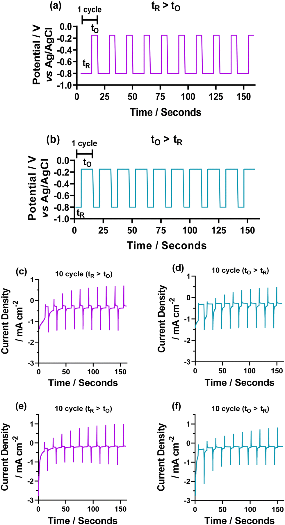 | ||
| Fig. 2 Figure showing the method of electrochemical deposition of Cu2+ to Cu thin films for the 10 cycle depositions. This method follows that a reducing potential (tR) is initially applied at −0.8 V, followed by an oxidative potential (tO) at −0.15 V. The two methods utilised in this report use either a reduction potential for twice the length of time as the oxidative potential (R > O, tR = 10 s, tO = 5 s) or the opposite (O > R, tR = 5 s, tO = 10 s). 1 cycle equated to both a tR and tO, voltages are referenced to Ag/AgCl. (c–f) Electrochemical deposition of Cu thin films for the (c and d) 5 mM Cu(Cl)2 with 5 mM NaCl system and (e and f) 5 mM Cu(Cl)2 50 mM NaCl system. Deposition was performed using chronoamperometry with −0.8 V (reducing potential) and −0.15 V (oxidising potential) vs. Ag/AgCl, with a 10 s:5 s ratio of deposition time, where tR > tO corresponds to a tR = 10 s and tO = 5 s and tO > tR corresponds to tR = 5 s and tO = 10 s. | ||
To analyse the deposited materials, powder X-ray diffraction (pXRD) and Raman spectroscopy were employed. Direct pXRD of the films was found to be ineffectual (Fig. S4, ESI†), due to the thin nature of the material (a monolayer thick, vide infra and cross-section SEM images Fig. S6, ESI†), Raman spectroscopy was used to structurally characterise the deposited material (Fig. S5, ESI†). Two peaks were observed, one centred ca. 525 cm−1, corresponding to the Raman allowed mode 3Γ′25(F2g),34 and perfectly matched the literature on Cu2O.34–36 The second peak found in our spectra centred ca. 600 cm−1. This observed peak is higher than the expected single peak for CuO (591 cm−1) but lower than the expected second peak corresponding to Cu2O (625 cm−1),35 although this is more consistent with the IR active mode  , reported as 608 cm−1.36 X-ray photoelectron spectroscopy (XPS) of the 30 cycle, 5 mM NaCl systems (Fig. S15–S17, ESI†) showed the presence of both Cu2O and Cu(0), but no CuO character, so the Raman peak at ca. 600 cm−1 can be discounted as CuO and is likely a strain effect red shifting the expected 625 cm−1 peak. XPS of these systems is discussed in more detail further below where anion effects were investigated. With these encouraging results suggesting that Cu2O was deposited, scanning electron microscopy (SEM) was next used to investigate the morphology of the deposited materials. Fig. 3 shows the deposited films for 10, 30 and 50 cycles of both tR > tO, and tO > tR for the 5 mM NaCl system (100 cycles shown in Fig. S7, ESI†). From this analysis, nanocubes were deposited from both systems, with dendritic materials deposited in the tR > tO system, and what resemble single crystal materials deposited in the tO > tR system. Quantitative analysis of the SEM images showed that the tR > tO method (purple in Fig. 3 bar charts) produced nanocubes that were, in general, both larger in size and broader in size distribution, compared to the tO > tR method (Table 1). The tO > tR method not only produced more homogenously sized nanocubes (Table 1), but consistently greater concentration of nanocubes compared to the equivalent cycle tR > tO method, and that increasing the number of cycles decreased the concentration of Cu nanocubes in both systems (Fig. 3(k)).
 | ||
| Fig. 3 Figure showing representative secondary electron SEM images of electrodeposited copper electrodes from the 5 mM CuCl2 and 5 mM NaCl solution with (a–c) 10 cycles, (d–f) 30 cycles and (h–j) 50 cycles where (a, d and h) tR > tO and (b, e and i) tO > tR. Also shown (c, f and j) are the relative distribution of copper oxide nanocubes throughout the image where purple is tR > tO and blue is tO > tR. All scale bars represent 1 μm, inset scale bars 250 nm. | ||
| Deposition cycles | Average nanocube size/nm | Nanocube concentration (×108)/cm−2 | ||
|---|---|---|---|---|
| t R > tO | t O > tR | t R > tO | t O > tR | |
| 10 | 132 ± 22 | 100 ± 10 | 3.2 ± 0.3 | 4.7 ± 0.3 |
| 30 | 136 ± 21 | 134 ± 15 | 2.0 ± 0.6 | 3.1 ± 0.2 |
| 50 | 180 ± 45 | 125 ± 20 | 1.4 ± 0.5 | 2.5 ± 0.2 |
| 100 | 297 ± 27 | 255 ± 33 | 1.0 ± 0.1 | 1.2 ± 0.1 |
SEM images of the high electrolyte, 50 mM NaCl system (Fig. S8, ESI†) found that formation of nanocubes was not possible to the degree of the low electrolyte systems, and quantitative analysis was not possible. This result is consistent with most of the literature on Cu-oxide nanomaterial electrodeposition, which use low concentrations of electrolytes,26–28,30–32,37 such as 5 mM CuSO4 with 5 mM NaCl,38 or 20 mM Cu(NO3)2.39 Although the reason low-electrolyte concentrations are required is not clear, some reports utilise high concentrations of electrolyte, such as 100 mM copper salt but significantly harsher deposition conditions (6 V) are required to form copper oxide nanomaterials.40 To the best of our knowledge, exactly why high concentration electrolytes are not capable of forming nanocubes under mild deposition conditions has not been reported.
Mimicking the high resistance environment of 5 mM NaCl supporting electrolyte with the 50 mM NaCl system
Increasing the concentration of supporting electrolyte in the system decreases both the RS and RET by increasing the solution conductivity.41 To determine if the formation of Cu2O nanocubes was caused by the high resistance environment created by low electrolyte concentration, we set out to mimic these high resistances, but with the high concentration (50 mM NaCl) system. This was achieved by increasing the inter-electrode separation between the working electrode and the counter and reference electrodes, up to 20 cm, in a 3-electrode setup (as shown visually in Fig. S9, ESI†). Prior to this being undertaken in the 50 mM NaCl system, a control experiment was initially conducted on the 5 mM NaCl system as it is possible to synthesise nanocubes with this electrolyte concentration. Fig. S10 (ESI†) shows the CV from increasing inter-electrode separation on the low concentration environment. A large increase in resistance as displayed by the significant reduction in current density and increase in the peak-to-peak separation is observed. Reproducible EIS analysis was not found to be possible on this system and cannot therefore be undertaken. Deposition from these systems was undertaken using the 30 cycle, tO > tR method only, and is shown in Fig. 4. It was found that the amount of copper deposited decreased with increasing inter-electrode separation (as expected by the lower current density observed in the CVs). This was exhibited by a significantly lower concentration of nanocubes when increasing the inter-electrode separation, which followed an approximately exponential decay as a function of inter-electrode separation (Fig. 4(f)). One unexpected outcome of this experiment was the increase in average size of deposited nanocubes, with increasing distance between electrodes (Fig. 4(e and f)). This followed a linear trend with ca. 1 cm (134 ± 15 nm), 2 cm (264 ± 38 nm), 5 cm (354 ± 46 nm), 10 cm (420 ± 76 nm) and 20 cm (763 ± 99 nm) (Fig. 4(f)) and could be used as a novel method of controlling the size of deposited nanocubes, although the homogeneity of nanocube size was found to decrease with increasing inter-electrode separation. It is also noteworthy that as the inter-electrode separation increased the proportion of non-cubic material deposited decreased, especially when up to 10 cm distance and above (Fig. 4(a–d)). | ||
| Fig. 4 Representative SEM images of the 5 mM CuCl2, 5 mM NaCl system with increasing inter-electrode separation between the working and counter and reference electrodes of (a) 2 cm, (b) 5 cm, (c) 10 cm and (d) 20 cm. Scale bars in main image are all 1 μm, inset 250 nm. (e) Distribution analysis for nanocube sizes where (grey) ∼1 cm, (red) 2 cm, (green) 5 cm, (purple) 10 cm and (orange) 20 cm inter-electrode separations have been assessed and (f) quantitative information on both nanocube concentration and size deposited with increasing electrode separation. The dashed lines are fittings for (blue) linear fit of nanocube size with increasing electrode separation and (orange) an exponential decay of nanocube concentration with increasing electrode separation. | ||
Having investigated this on the 5 mM system, the 50 mM system was next investigated. CV and EIS analysis was undertaken using this setup and are shown in Fig. 5. As shown in Fig. 5(c), both RS and RET increase to values comparable with the low-concentration system (RS of 649 Ω vs. 614 Ω and RET of 619 Ω vs. 790 Ω, respectively). SEM analysis of deposited materials at various inter-electrode separations in the high concentration environment determined that high concentration formation of nanocubes was not achieved, even at comparable resistances. Although some nanocube formation was found to be possible (Fig. S12, ESI†). These results show that despite having a high resistance in high electrolyte concentration conditions, it is still not possible to achieve high concentrations of nanocubes. It is therefore another factor which drives nanocube formation, or that nanocube formation is prevented simply by having high electrolyte concentrations. However, we did not investigate this any further.
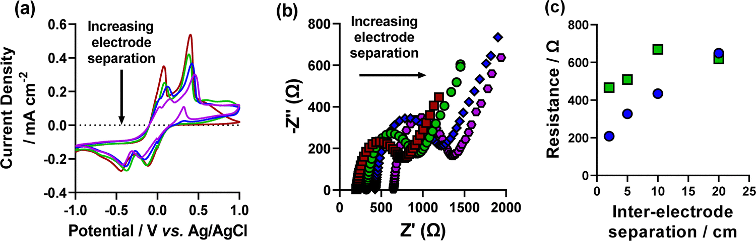 | ||
| Fig. 5 CVs of the increasing inter-electrode separation between the working electrode and the counter and reference electrodes where red (2 cm), green (5 cm), blue (10 cm), purple (20 cm). (b) EIS Nyquist plots of increasing inter-electrode separation where red squares (2 cm), green circles (5 cm), blue diamonds (10 cm) and purple hexagons (20 cm) are shown. Also shown in (c) the measured resistance from the inter-electrode separation Nyquist plots in (b) (fitting shown in Fig. S11, ESI†) of the (blue circles) RS and (green squares) RET. | ||
Mixed-anionic environment effects
As discussed in the introduction, most fundamental Cu-oxide nanomaterial deposition reports use an environment which contains an anion combination from a copper salt such as nitrate, sulphate, or acetate, with additional NaCl as a [Cl]− source. To investigate if the mixed anion environment is beneficial for Cu-oxide nanocube formation, we set out to investigate the effect of having a mixed-anion environment using 5 mM NaCl, with either 5 mM Cu(Cl)2 (Cl only), Cu(CH3CO2)2 ([CH3CO2]/[Cl]), Cu(NO3)2 ([NO3]/[Cl]) or Cu(SO4) ([SO4]/[Cl])§ as the copper source. These systems were initially assessed for their fundamental electrochemical properties by CV and EIS analysis. Fig. 6(a and b) show the recorded CV of all four systems. The CV analysis showed a significantly higher oxidative current in the [SO4]/[Cl] system, however the current was not significantly higher than the [NO3]/[Cl] system in the reductive wave. It is not known why this oxidative current is much higher in the [SO4]/[Cl] system, but this could be due to the higher ionic strength of the system which was used to balance the [A]/[Cl] ratio (Table S3, ESI†). Previous fundamental studies on the kinetics of copper electrodeposition from copper sulphate at a rotating disc electrode have shown that the formation of univalent copper ions in the stripping process reduces the current efficiency in the cathodic (deposition) process, with similar effects possibly occurring here.42,43 | ||
| Fig. 6 (a and b) Cyclic voltammograms (CVs) of 5 mM of various Cu salts: blue Cu(Cl)2, green Cu(CH3CO2)2, red Cu(NO3)2 and orange CuSO4 in the presence of 5 mM NaCl for all systems with the exception of the sulphate system which also contains 5 mM of Na2SO4 to maintain an equivalent anion concentration. These were recorded on an ITO-coated glass substrate with a Ag/AgCl reference electrode and a copper wire counter electrode at a scan rate of 50 mV s−1. (c and d) Electrochemical impedance spectroscopy of the four investigated copper systems with various counter ion combinations where (c) shows the Nyquist plots of blue Cu(Cl)2, green Cu(CH3CO2)2, red Cu(NO3)2 and orange CuSO4 in the presence of 5 mM NaCl for all systems with the exception of the sulphate system which also contains 5 mM of Na2SO4 to maintain an equivalent anion concentration. (d) Measured solution (RS) and electron transfer (RET) resistances of the various copper systems from the impedance spectroscopy where the left bars represent RS and the right bars represent RET. | ||
The EIS analysis (Fig. 6(c and d), fitting shown in Fig. S13, ESI†) showed the [SO4]/[Cl] and [NO3]/[Cl] systems to have a lower RS and RET than the other systems, which is consistent with the higher observed current density of the CVs. Another interesting trend in these systems is that the lower resistance [SO4]/[Cl] and [NO3]/[Cl] systems have higher RS than RET and the higher resistance [Cl] only and [CH3CO2]/[Cl] systems observe higher RET than RS. Further fundamental analysis was conducted on these mixed anionic environments compared to the pure Cl-only systems. The open-circuit potential (VOCP) of the five systems was measured. The VOCP of the Cl-only systems was significantly higher (213 ± 6 and 264 ± 3 mV for the 5 mM NaCl and 50 mM NaCl, respectively) than the mixed systems (155 ± 3 mV, 170 ± 9 mV, and 176 ± 3 mV for the [CH3CO2]/[Cl], [NO3]/[Cl] and [SO4]/[Cl] systems, respectively), indicative of a stronger oxidising environment inherent in the [Cl]-only system. The conductivity of the different environment solutions was measured to determine the effect of higher ionic strength of the [SO4]/[Cl] system (60 mM vs. 25 mM), and lower dissociation strength of the [CH3CO2]− anion. This analysis found that the conductivity of the mixed solutions increases in the order [CH3CO2]/[Cl] (1.07 mS cm−1) > [Cl]-only (1.24 mS cm−1) > [NO3]/[Cl] (1.71 mS cm−1) > [SO4]/[Cl] system (2.06 mS cm−1).
For copper oxide nanomaterial deposition from these systems, 30 cycles of tR > tO and tO > tR were used. Raman analysis (Fig. S14, ESI†) of the deposited materials in these environments was found to be consistent with the Cl-only systems (Fig. S5, ESI†), and again with previously reported copper oxide nanomaterial investigations.44 XPS analysis (survey spectra shown in Fig. S15 (ESI†), Cu 2p spectra shown in Fig. S14, ESI†) was also undertaken on these samples. The Cu 2p spectra of all samples showed two peaks centred ca. 952 eV (Cu 2p1/2) and 932 eV (Cu 2p3/2) eV. The tR > tO [NO3]/[Cl] system was found to show the satellite peaks consistent with CuO (i.e. the Cu(II) oxidation state), which was not present in the tO > tR [NO3]/[Cl] system, or any of the other systems. As the Cu(0) and Cu2O positions overlap in this region,37,45 these cannot be discerned from the 2p spectra alone, therefore the Auger spectra was also measured. From this, the [Cl]− only, [CH3CO2]/[Cl] and [SO4]/[Cl] systems were all found to display peaks which correspond to both Cu2O and Cu (Fig. S17, ESI†).
The [CH3CO2]/[Cl] tR > tO deposition was found to achieve significant nanocube formation (Fig. 7). The average size of these nanocubes was found to be significantly larger than the comparable [Cl]-only system (392 ± 55 vs. 136 ± 21 nm, respectively). Nanocube formation was found to be possible with the [CH3CO2]/[Cl] tO > tR system, but significantly less than the tR > tO equivalent and not sufficient to undertake any reasonable quantitative analysis. Both [CH3CO2]/[Cl] systems also formed dendritic material and what appear to be smaller particles which could be seeds for the dendrites or nanocubes. The [NO3]/[Cl] tO > tR system was also able to form nanocubes (202 ± 52 nm), along with both dendrites and smaller unorganised shaped particles. Contrary to recent literature which observed formation of copper oxide nanocubes on glassy carbon31 and platinum46 electrodes using a CuSO4 and NaCl environment (our mixed [SO4]/[Cl] system), was not able to form nanocubes, however, the system investigated here is significantly different from those previously reported such as using a different working electrode surface (ITO here), and varying levels of inherent electrolyte (we employ added Na2SO4 in our [SO4]/[Cl] system to maintain a consistent [SO4]:[Cl] ratio as the [NO3] and [CH3CO2] systems), which gives both higher ionic strength and conductivity, and lower resistance than the other systems investigated here. Having demonstrated that the presence of [Cl]− is clearly not the only factor involved in formation of Cu2O nanocubes, we set out to investigate if a mono-anionic environment can also achieve nanocube formation (in the absence of [Cl]−), and what environmental conditions these systems have.
 | ||
| Fig. 7 Figure showing representative SEM images of (a and b) 5 mM CuCl2 with 5 mM NaCl, (c and d) 5 mM Cu(CH3CO2)2 with 5 mM NaCl, (e and f) 5 mM Cu(NO3)2 with 5 mM NaCl, (g and h) 5 mM CuSO4 with 5 mM NaCl and 5 mM Na2SO4. (a, c, e and g) are from tR > tO depositions and (b, d, f and h) are from tO > tR depositions. Scale bars of images 1 μm, insets 250 nm. | ||
Mono-anionic environments
The mono-anionic environments of [CH3CO2]−, [NO3]− and [SO4]2− were investigated using the respective copper and sodium salts to maintain an anion ([A]) concentration of 15 mM. Again, the fundamental electrochemical properties of these environments were assessed. The [CH3CO2] and [NO3] systems were found to show less well formed voltammograms than the mixed [A]/[Cl] systems (Fig. 8(a and b)). Although the [SO4] system was again found to have a high oxidative current and a well-formed voltammogram, which again is likely due to the higher ionic strength (80 mM) environment required to maintain a consistent [SO4] concentration. | ||
| Fig. 8 (a and b) Cyclic voltammograms (CVs) of 5 mM of various Cu salts: blue Cu(Cl)2, green Cu(CH3CO2)2, red Cu(NO3)2 and orange CuSO4 in the presence of 5 mM Na[A] where [A] represents the anion of the corresponding copper salt. These were recorded on an ITO-coated glass substrate with a Ag/AgCl reference electrode and a copper wire counter electrode at a scan rate of 50 mV s−1. Electrochemical impedance spectroscopy of the four investigated copper systems with various counter ion combinations where (c) shows the Nyquist plots of blue Cu(Cl)2, green Cu(CH3CO2)2, red Cu(NO3)2 and orange CuSO4 in the presence of 5 mM Na[A] where [A] represents the anion of the corresponding copper salt. (d) Measured solution (RS) and electron transfer (RET) resistances of the various copper systems from the impedance spectroscopy where the left bars represent RS and the right bars represent RET. | ||
EIS analysis (Fig. 8(c and d), fitting in Fig. S18, ESI†) of these systems found that consistently higher resistances in all systems was observed compared to their mixed environment equivalents. The [NO3]-only system found a significantly higher resistance than the [NO3]/[Cl] system, which is the cause of the poorly formed voltammogram (Fig. 8). Another interesting result from this analysis is that all mono-anionic environments have a higher RET than RS, where this was only found in the [Cl]-only and [CH3CO2]/[Cl] systems in the mixed anionic environments. Thin film Cu-nanomaterials were deposited from these systems using the 30 cycle tR > tO and tO > tR methodology employed in the mixed systems. Raman analysis of these systems from the mono-anionic environments was again found to be consistent with the Cu-only system, and the mixed [A]/[Cl] systems (Fig. S19, ESI†). XPS analysis (survey spectra Fig. S20, 2p Fig. S21 and Auger Fig. S22, ESI†) again showed that only the [NO3] environment deposited with tR > tO method is the only film with the signature CuO satellite peaks in the 2p spectra. The Auger spectra of these systems for both [CH3CO2] and [SO4] and the [NO3] tO > tR systems is consistent with a majority of Cu2O, and a small shoulder consistent with Cu(0). The [NO3] tR > tO Auger spectra showed a single, broad peak over both the expected positions for Cu2O and CuO, which is consistent with the Cu 2p spectra.
The VOCP of these mono-anionic environments was also measured, these were all found to be lower than the mixed [A]/[Cl] systems, with the [CH3CO2], [SO4] and [NO3] systems having a VOCP of 123 ± 6 mV, 119 ± 3 mV, and 129 ± 3 mV, respectively, demonstrating an inherently lower oxidising environment in the (non-[Cl]) mono-anionic environments than the mixed systems. pH is an important factor in directing the formation of copper nanocubes, as pH is crucial for oxidation state selection.32 Low pH environments have also been shown to significantly reduce the voltametric response of Cu2+ ions.43 Due to this, the pH of all investigated systems was measured. All systems were found to observe a pH between 5 and 6 with the [Cl]-only system (5.32) the most acidic and the [CH3CO2]-only system the most basic (6.00).
SEM analysis showed that the [CH3CO2]-only deposited films were found to form octahedra structures (Fig. 9(d)). This is consistent with the [CH3CO2]-only environment favouring the {111} growth plane, as demonstrated by previous studies.47 SEM analysis of the deposited thin films also showed that significant nanocube formation was possible for the [NO3] tO > tR system (Fig. 9(f)). The formed nanocubes were far more concentrated (1.13 × 10⁹ ± 1.00 × 108 cm−2) (N.B. this is an ca. 2-fold greater concentration that the next highest, Table S4, ESI†) and more homogenously sized (181 ± 2 nm) than all other investigated systems. The [SO4]-only system was also found to form nanocubes with the tO > tR method, which are small (104 ± 14 nm) and of equivalent concentration (7.28 × 10⁸ ± 7.28 × 10⁷) to the mixed [CH3CO2]/[Cl] and [NO3]/[Cl] systems and over 2-fold higher concentration than the [Cl]-only deposited films (all data Tabulated in Table S4, ESI†). These are significant observations, as mixed anionic environments are almost exclusively utilised in the literature, with recent literature reporting the importance for the presence of [Cl] in solution for the formation of copper oxide nanocubes. Yet here we found that under certain environmental conditions in the absence of [Cl], the mono-anionic environments yield more homogenously sized and more concentrated (i.e. more control in deposition) nanocube formation than the mixed anionic environments containing [Cl] or the mono-anionic [Cl] environment.
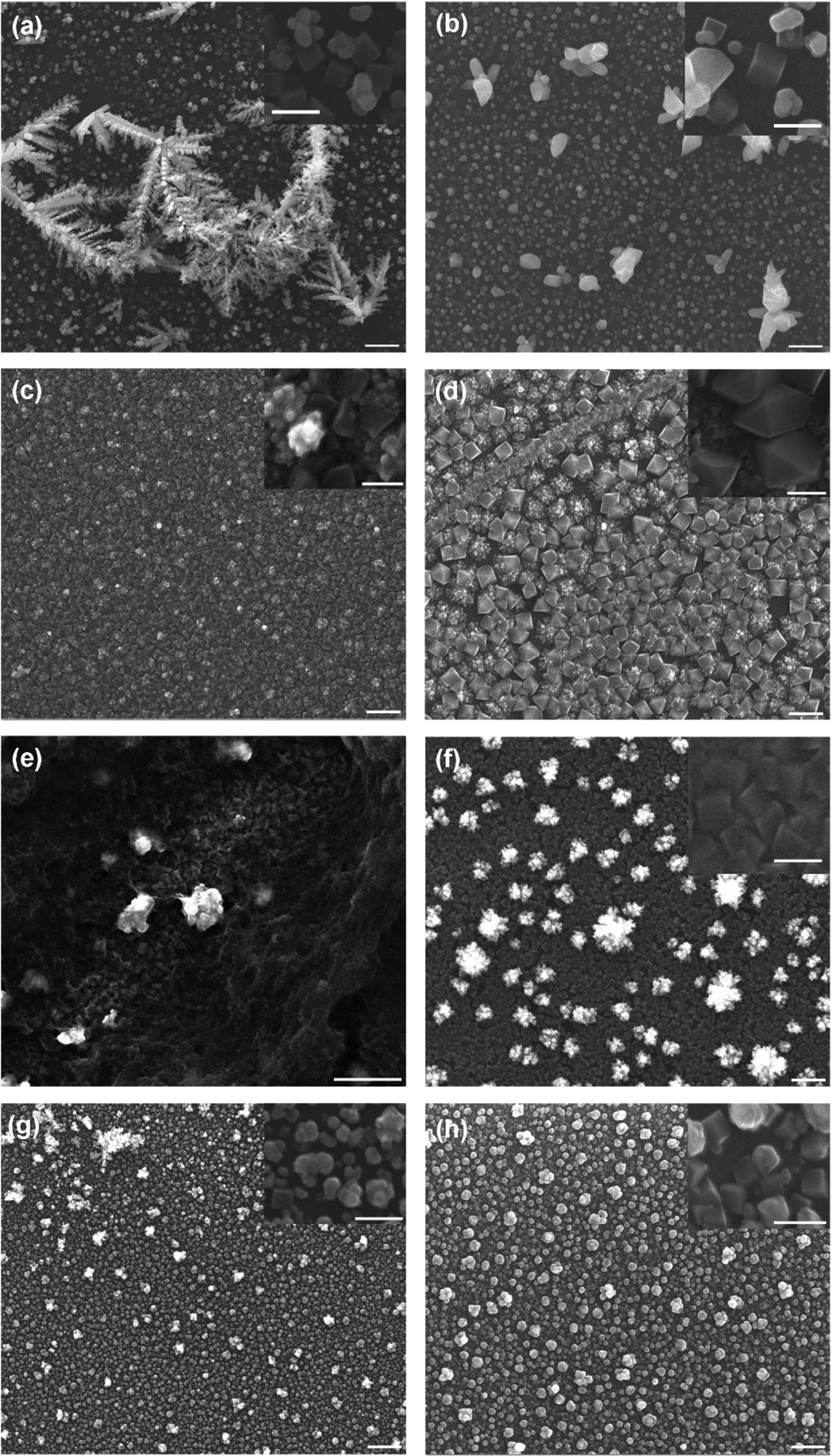 | ||
| Fig. 9 Figure showing representative SEM images of (a and b) 5 mM CuCl2 with 5 mM NaCl, (c and d) 5 mM Cu(CH3CO2)2 with 5 mM NaCH3CO2, (e and f) 5 mM Cu(NO3)2 with 5 mM NaNO3, (g and h) 5 mM CuSO4 with 10 mM Na2SO4. (a, c, e and g) are from tR > tO depositions and (b, d, f and h) are from tO > tR depositions. Scale bars of images 1 μm, insets 250 nm. N.B. The NO3-only system deposited by tR > tO (e) was found to be highly charging at higher magnifications and we were not able to obtain a good quality magnified image as obtained in all other systems. | ||
Properties of deposited films
The thin film Cu nanomaterial electrodes were measured for their optical and electronic properties. Cu2O is reported with a direct band gap energy (Eg) between 2.0–2.2 eV, which is commensurate with visible light photon absorption.2 The optical properties of our deposited thin films were therefore measured by UV-Vis spectroscopy, the resultant spectra are shown in Fig. S23 (ESI†). Deposition in different environments yielded films with different colouration, for example the [CH3CO2]-only system yielded a dark purple (Fig. 10(c(i))), [SO4]-only a light pink (Fig. 10(c(ii))) and [NO3]-only a pale yellow (Fig. 10(c(iii))). Due to the different observed colours in the synthesised thin films, they clearly absorb different parts of the visible spectrum. Therefore, it is expected that these films would have different Eg. Therefore, the optical band gaps of these materials were determined via Tauc plots (Fig. 10(a and b) for the mono-anion environments and Fig. S24, ESI†) and are plotted in Fig. 10(c). From this analysis, it is clear that the mono-anionic environments show higher optical Eg than the mixed anionic systems where the [CH3CO2]-only (2.11 and 2.19 eV), [NO3]-only (2.47 and 2.53 eV) and [SO4]-only (1.73 and 1.74 eV) show higher Eg than the [CH3CO2]/[Cl] (1.36 and 1.74 eV), [NO3]/[Cl] (2.34 and 1.96 eV) and [SO4]/[Cl] (1.54 and 1.72 eV) for the tR > tO and tO > tR, respectively. Overall, there is a wide range of optical Eg from these materials, with the lowest Eg of [CH3CO2]/[Cl] (tR > tO) showing an optical Eg of 1.36 eV and the [NO3]-only (tO > tR) showing an optical Eg of 2.53 eV. It has previously been demonstrated that the surface structure and size of Cu2O nanomaterials has a significant impact on the band gap energy of the material.5 Computational analysis has also shown that lattice strain has a large impact on the band gap of Cu2O, with computationally determined values between 1.1–2.2 eV.48 Therefore, we can attribute the range of band gap energies observed here to the various morphologies, sizes, and possibly strain of the deposited Cu-oxide nanomaterials deposited. This analysis also showed that it is possible to tailor the band gap energy of the Cu-oxide materials using the various environments investigated here, which could have a significance for photoelectrocatalysis and heterojunction solar cells developed using Cu2O.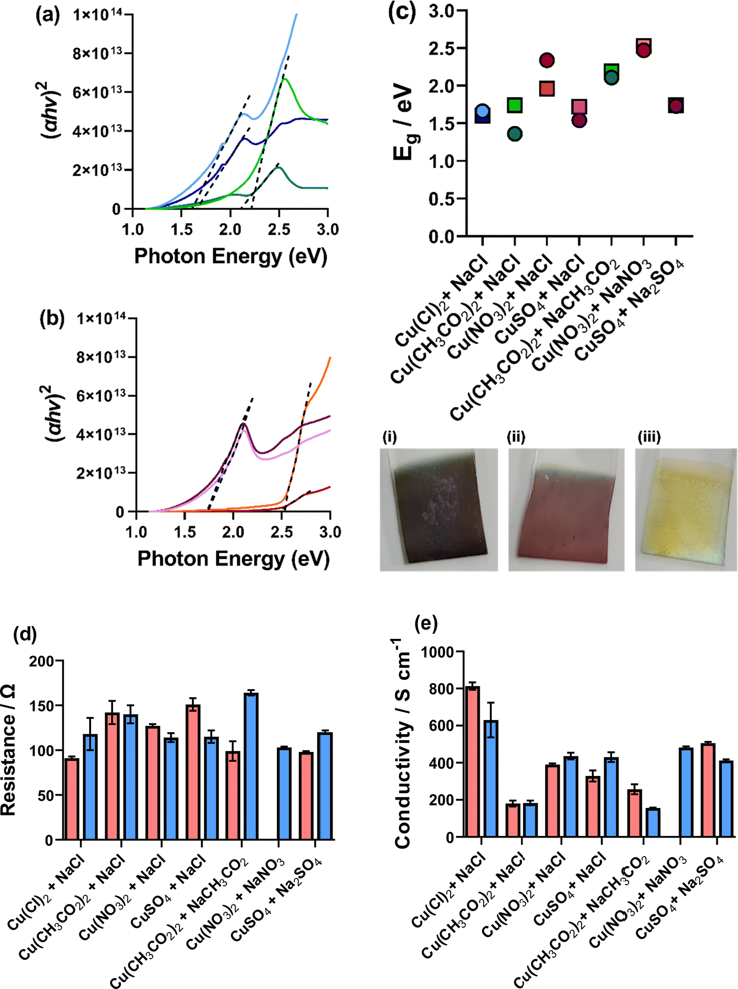 | ||
| Fig. 10 Figure showing (a and b) Tauc plots of (a) [Cl]-only, (blue), (b) [CH3CO2]-only (green) and (b) [NO3]-only (red) and [SO4]-only (purple) where the tR > tO deposition is the dark colour and the tO > tR is the light colour. Also shown in (c) is the calculated band gap energies (where circles represent tR > tO and squres represent tO > tR) from the Tauc analysis (Fig. S21, ESI†) and representative deposited films for (i) [CH3CO2]-only, (ii) [SO4]-only and (iii). [NO3]-only. (d) The measured resistance and (e) the measured conductivity of the ITO/Cu2O deposited materials. | ||
The absolute resistance, resistivity, and conductivity of the films was also measured using a 4-point probe.¶Fig. 10(d and e) show the resistance and conductivity of all measured films. The [NO3]-only tR > tO was found to deposit an insulating layer and could not be measured. Absolute resistance was measured of the bare ITO prior to any Cu2O deposition and found to be 105 ± 1 Ω. The ITO/Cu2O electrodes were found to be between 91 ± 2 Ω for the (tR > tO) CuCl2, 5 mM NaCl system to 164 ± 3 Ω for the (tO > tR) Cu(CH3CO2)2, 5 mM NaCH3CO2 system, showing that depending on the deposition environment the electrode resistance can be improved upon (full data for all deposited environments shown in Table S3, ESI†). The [CH3CO2]/[Cl] and [CH3CO2]-only films were found to show low conductivity compared to the others and the [Cl]-only systems were found to have higher conductivity. However, all films were found to yield film conductivity between 200–800 S cm−1, which is high for semiconductor materials,6 and could potentially be enhanced due to the presence of metallic Cu(0) (as observed by XPS). The mono-anionic environment-deposited thin films were generally found to yield higher conductivity than the mixed anionic environments (Fig. 10(e)), again demonstrating that towards applications the mono-anionic environments are preferential, with better control of nanomaterial deposition and higher film conductivity. A comprehensive Table of data for ionic strength, pH, conductivity, VOCP, RS, RET, jp, deposited film conductivity, band gap energy and deposited nanocube properties can be found in Tables S3 and S4 (ESI†).
Possible correlations between physiochemical and electrochemical properties of the solution and the electronic and optical properties of the deposited thin films
As shown in Table S3 (ESI†), data has been measured for the physiochemical (ionic strength, pH, and solution conductivity, κ) and electrochemical (VOCP, RS, RET) properties of each environment, along with electrochemical (jp), optical (Eg), and electronic (conductivity, σ) properties of the deposited thin films. We next set out to use this comprehensive dataset to assess if any potential correlations between physiochemical, electrochemical, optical, and electronic properties could be determined. Currently no means of predicting optical and electronic properties of deposited films exist from the physiochemical or electrochemical properties of the solutions. This would be extremely valuable given the ease of measuring physiochemical properties of solutions and undertaking electrochemical analysis of solutions.
Fig. 11 shows a correlogram from the requisite dataset. The size of the circle and the darkness of the colour both visually demonstrate the magnitude of a correlation (rxy, known as the Pearson correlation, where an ideal correlation = 1) between two given data sets, with larger circle and darker colour both representing a stronger correlation, with red representing a positive correlation and blue a negative correlation. From this analysis, some expected correlations are confirmed, such as the strong positive correlation between solution conductivity (κ) and ionic strength,41 and the strong negative correlation between these two parameters and solution resistance, which follow the relationship:  where A and l are a bounded area and length, respectively.41 From our correlation analysis κ was found to observe a strong positive correlation with ionic strength (0.93) and RS a strong negative correlation to both κ (−0.80) and ionic strength (−0.80).
 | ||
| Fig. 11 Correlogram exploring correlation between solution physiochemical, solution electrochemical and electrochemical deposition and thin film electronic and photochemical properties. | ||
We next searched for any correlations between the physiochemical properties of the solutions and the electronic and optical properties of the films. The solution pH was found to strongly correlate with the film resistance (0.87) and conductivity (0.94) of the tO > tR method-deposited films, but not to the tR > tO method-deposited films. This correlation indicates that measuring pH could be a possible route towards predicting thin film conductivity of the tO > tR deposited films. Other correlations were found from this analysis, involving jp. Here, jp (or peak current density) is taken from the 30th oxidative cycle during deposition. As shown in Fig. 2(c–f), oxidative jp increases with increasing number of cycles. This is due to the increased concentration of deposited copper (from each tR cycle), as the tO only oxidised the deposited Cu(0) to Cu2O.31 Therefore, jp can be treated as a pseudo-electrochemically active surface area (ECSA). jp was found to correlate well with solution VOCP for the tO > tR (0.83) and tR > tO (0.82) deposition methods, along with the κ, again for both tO > tR (0.79) and tR > tO (0.81) deposition methods. jp from the tO > tR deposited systems were also found to strongly correlate with film conductivity for the tO > tR (0.85), although a poor correlation was found between the jp from the tR > tO deposited films and the film conductivity for the tR > tO deposited film (0.59). This is likely due to the different nature of the tR > tO deposited films and the tO > tR deposited films discussed throughout this report. No prior relationships could be found for these correlations between physiochemical solution properties and electrochemical and film electronic properties. Again, demonstrating that analysis such as this could lead to predictive relationships of physiochemical, electrochemical, and optical and electronic effects between solutions or thin films.
Conclusions
We set out to undertake a synthetic study towards the synthesis of Cu2O nanocubes by utilising electrodeposition from copper salts (chloride, acetate, nitrate, and sulphate) in different solution environments. It was found that low-electrolyte concentrations were required to synthesise high quantities of copper oxide nanocubes, and that by increasing the resistance of the system by increasing the inter-electrode separation the size of the deposited nanocubes could be controlled. Both mixed anion environments and mono-anion electrolyte environments were also investigated in a low-electrolyte concentration system. The fundamental physiochemical and electrochemical properties of each solution such as pH, conductivity, open circuit potential (VOCP), solution resistance (RS), and electron transfer resistance (RET) were measured, and copper oxide nanomaterial thin films were deposited on ITO-coated glass substrates. The electrical (conductivity) and optical (Eg) properties of these films were also determined through 4-point probe and UV-Vis analysis. Using the comprehensive dataset measured in this project, we set out to determine if any possible correlations could be drawn between the physiochemical and electrochemical properties of the solution and the electronic and optical properties of the deposited Cu2O thin films. This analysis showed that pH correlated well with the film resistance and σ of the tO > tR-deposited films and that jp (or pseudo-ECSA) correlated well with solution VOCP and κ for both tO > tR and tR > tO deposited films.Author contributions
The project was conceptualised and undertaken by M. A. B. W. X., and B. W.-O’. B. undertook the electron microscopy. K. Y. provided industrial input and the correlation study. U. S., A. M. and D. J. L. were responsible for funding acquisition. B. F. S. contributed the experimental work and expertise for XPS. A. M. and D. J. L. were responsible for supervision. All authors contributed to manuscript preparation which was finalised by M. A. B., A. M., and D. J. L.Conflicts of interest
There are no conflicts of interest to declare.Acknowledgements
The authors would like to acknowledge the funding and technical support from bp through the bp International Centre for Advanced Materials (bp-ICAM), which made this research possible. W. X. thanks Beihang University for the opportunity to come to Manchester. B. W.-O’. B. is funded by an EPSRC DTA studentship. B. S. acknowledges support for the XPS at UoM by the Henry Royce Institute for Advanced Materials, funded through EPSRC grants EP/R00661X/1, EP/S019367/1, EP/P025021/1, and EP/P025498/1.References
- T. K. S. Wong, S. Zhuk, S. Masudy-Panah and G. K. Dalapati, Materials, 2016, 9 Search PubMed.
- A. M. Mohammed, S. S. Mohtar, F. Aziz, S. A. Mhamad and M. Aziz, J. Environ. Chem. Eng., 2021, 9, 105138 CrossRef CAS.
- R. M. Arán-Ais, F. Scholten, S. Kunze, R. Rizo and B. Roldan Cuenya, Nat. Energy, 2020, 5, 317–325 CrossRef.
- T. Möller, F. Scholten, T. N. Thanh, I. Sinev, J. Timoshenko, X. Wang, Z. Jovanov, M. Gliech, B. Roldan Cuenya, A. S. Varela and P. Strasser, Angew. Chem., Int. Ed., 2020, 59, 17974–17983 CrossRef PubMed.
- B. Sinha, T. Goswami, S. Paul and A. Misra, RSC Adv., 2014, 4, 5092–5104 RSC.
- A. Zakutayev, V. Stevanovic and S. Lany, Appl. Phys. Lett., 2015, 106, 123903 CrossRef.
- A. Osherov, C. Zhu and M. J. Panzer, J. Phys. Chem. C, 2013, 117, 24937–24942 CrossRef CAS.
- Z. Zolfaghari-Isavandi and Z. Shariatinia, J. Alloys Compd., 2018, 737, 99–112 CrossRef CAS.
- P. Grosse, D. Gao, F. Scholten, I. Sinev, H. Mistry and B. Roldan Cuenya, Angew. Chem., Int. Ed., 2018, 57, 6192–6197 CrossRef CAS PubMed.
- G. L. De Gregorio, T. Burdyny, A. Loiudice, P. Iyengar, W. A. Smith and R. Buonsanti, ACS Catal., 2020, 10, 4854–4862 CrossRef CAS PubMed.
- M. Gattrell, N. Gupta and A. Co, J. Electroanal. Chem., 2006, 594, 1–19 CrossRef CAS.
- W. Ye, X. Guo and T. Ma, Chem. Eng. J., 2021, 414, 128825 CrossRef CAS.
- D. Wakerley, S. Lamaison, F. Ozanam, N. Menguy, D. Mercier, P. Marcus, M. Fontecave and V. Mougel, Nat. Mater., 2019, 18, 1222–1227 CrossRef CAS PubMed.
- S. Ahn, K. Klyukin, R. J. Wakeham, J. A. Rudd, A. R. Lewis, S. Alexander, F. Carla, V. Alexandrov and E. Andreoli, ACS Catal., 2018, 8, 4132–4142 CrossRef CAS.
- X. Chen, J. Chen, N. M. Alghoraibi, D. A. Henckel, R. Zhang, U. O. Nwabara, K. E. Madsen, P. J. A. Kenis, S. C. Zimmerman and A. A. Gewirth, Nat. Catal., 2021, 4, 20–27 CrossRef CAS.
- S. Nitopi, E. Bertheussen, S. B. Scott, X. Liu, A. K. Engstfeld, S. Horch, B. Seger, I. E. L. Stephens, K. Chan, C. Hahn, J. K. Nørskov, T. F. Jaramillo and I. Chorkendorff, Chem. Rev., 2019, 119, 7610–7672 CrossRef CAS PubMed.
- A. Bagger, W. Ju, A. S. Varela, P. Strasser and J. Rossmeisl, ChemPhysChem, 2017, 18, 3266–3273 CrossRef CAS PubMed.
- S. Nitopi, E. Bertheussen, S. B. Scott, X. Liu, A. K. Engstfeld, S. Horch, B. Seger, I. E. L. Stephens, K. Chan, C. Hahn, J. K. Nørskov, T. F. Jaramillo and I. Chorkendorff, Chem. Rev., 2019, 119, 7610–7672 CrossRef CAS PubMed.
- Y. I. Hori, Electrochemical CO2 reduction on metal electrodes, Springer, 2008 Search PubMed.
- C. H. Kuo and M. H. Huang, Nano Today, 2010, 5, 106–116 CrossRef CAS.
- C. H. Kuo and M. H. Huang, J. Phys. Chem. C, 2008, 112, 18355–18360 CrossRef CAS.
- S. Sun, X. Song, Y. Sun, D. Deng and Z. Yang, Catal. Sci. Technol., 2012, 2, 925–930 RSC.
- E. G. Ponyatovskii, G. E. Abrosimova, A. S. Aronin, V. I. Kulakov, I. V. Kuleshov and V. V. Sinitsyn, Phys. Solid State, 2002, 44, 852–856 CrossRef CAS.
- P. He, X. Shen and H. Gao, J. Colloid Interface Sci., 2005, 284, 510–515 CrossRef CAS PubMed.
- H. Yu, J. Yu, S. Liu and S. Mann, Chem. Mater., 2007, 19, 4327–4334 CrossRef CAS.
- M. J. Siegfried and K. S. Choi, J. Am. Chem. Soc., 2006, 128, 10356–10357 CrossRef CAS PubMed.
- M. J. Siegfried and K.-S. Choi, Angew. Chem., 2005, 117, 3282–3287 CrossRef.
- M. J. Siegfried and K. S. Choi, Adv. Mater., 2004, 16, 1743–1746 CrossRef CAS.
- J. Timoshenko, A. Bergmann, C. Rettenmaier, A. Herzog, R. M. Arán-ais, H. S. Jeon, F. T. Haase, U. Hejral, P. Grosse, S. Kühl, E. M. Davis, J. Tian, O. Magnussen and B. R. Cuenya, Nat. Catal., 2022, 5, 259–267 CrossRef CAS.
- R. M. Arán-Ais, R. Rizo, P. Grosse, G. Algara-Siller, K. Dembélé, M. Plodinec, T. Lunkenbein, S. W. Chee and B. Roldan Cuenya, Nat. Commun., 2020, 11, 1–8 CrossRef PubMed.
- P. Grosse, A. Yoon, C. Rettenmaier, S. W. Chee and B. Roldan Cuenya, J. Phys. Chem. C, 2020, 124, 26908–26915 CrossRef CAS PubMed.
- Y. C. Sun, C. Y. Sun, Z. X. Chen, P. Wang, H. T. Wang, M. Z. Yao, S. Wu and P. Xu, Inorg. Chem. Front., 2021, 8, 1449–1454 RSC.
- N. Farley, https://www.casaxps.com, 2019.
- A. Singhal, M. R. Pai, R. Rao, K. T. Pillai, I. Lieberwirth and A. K. Tyagi, Eur. J. Inorg. Chem., 2013, 2640–2651 CrossRef CAS.
- Y. Deng, A. D. Handoko, Y. Du, S. Xi and B. S. Yeo, ACS Catal., 2016, 6, 2473–2481 CrossRef CAS.
- G. Niaura, Surface-enhanced Raman spectroscopic observation of two kinds of adsorbed OH − ions at copper electrode, 2000, vol. 45 Search PubMed.
- R. Arrigo, R. Blume, A. I. Large, J. J. Velasco-Vélez, M. Hävecker, A. Knop-Gericke and G. Held, Faraday Discuss., 2022, 236, 126–140 RSC.
- P. Grosse, A. Yoon, C. Rettenmaier, S. W. Chee and B. Roldan Cuenya, J. Phys. Chem. C, 2020, 124, 26908–26915 CrossRef CAS PubMed.
- M. J. Siegfried and K. S. Choi, Adv. Mater., 2004, 16, 1743–1746 CrossRef CAS.
- Y. C. Sun, C. Y. Sun, Z. X. Chen, P. Wang, H. T. Wang, M. Z. Yao, S. Wu and P. Xu, Inorg. Chem. Front., 2021, 8, 1449–1454 RSC.
- A. J. Bard and L. R. Faulkner, Electrochemical Methods: Fundamentals and Applications, John Wiley & Sons, Inc., 2nd edn, 2001 Search PubMed.
- A. I. Danilov, E. B. Molodkina and Y. M. Polukarov, Initial Stages of Copper Electrocrystallization from Sulfate Electrolytes: Cyclic Voltammetry on a Platinum Ring-Disk Electrode, 2000, vol. 36 Search PubMed.
- A. I. Davilov, E. B. Molodkina and Y. M. Polukarov, Russ. J. Electrochem., 2002, 38, 732 CrossRef.
- Y. Deng, A. D. Handoko, Y. Du, S. Xi and B. S. Yeo, ACS Catal., 2016, 6, 2473–2481 CrossRef CAS.
- M. C. Biesinger, Surf. Interface Anal., 2017, 49, 1325–1334 CrossRef CAS.
- R. M. Arán-Ais, R. Rizo, P. Grosse, G. Algara-Siller, K. Dembélé, M. Plodinec, T. Lunkenbein, S. W. Chee and B. Roldan Cuenya, Nat. Commun., 2020, 11, 1–8 CrossRef PubMed.
- S. Sun, D. Deng, C. Kong, Y. Gao, S. Yang, X. Song, B. Ding and Z. Yang, CrystEngComm, 2011, 13, 5993–5997 RSC.
- A. Visibile, R. B. Wang, A. Vertova, S. Rondinini, A. Minguzzi, E. Ahlberg and M. Busch, Chem. Mater., 2019, 31, 4787–4792 CrossRef CAS.
Footnotes |
| † Electronic supplementary information (ESI) available. See DOI: https://doi.org/10.1039/d2tc04662h |
| ‡ When using a Pt wire in our setup, the use of counter electrode material was found to have a significant effect on formation of Cu2O nanocubes (Table S1, ESI†). |
| § It should be noted here that the Cu(SO4) system included an additional 5 mM of Na2SO4 to ensure a comparable [A]/Cl ratio. |
| ¶ It should be noted that the resistance, resistivity, and conductivity of the films is of the ITO/Cu-deposit prepared electrode and not compensated for by the ITO. |
| This journal is © The Royal Society of Chemistry 2023 |