
 Open Access Article
 This Open Access Article is licensed under a Creative Commons Attribution-Non Commercial 3.0 Unported Licence
Multi-dimensional dynamic fluorescence readout from laser engineered In2O3 nanowire micropatterns†
Eng Tuan
Poh
 ab,
Yung Zhen
Tan
c,
Justin Boon Shuan
Neo
c,
Chee How
Ong
c,
Azianty
Saroni
d,
Zheng
Zhang
e,
Jianhui
Li
b,
Boon Tong
Goh
*d and
Chorng Haur
Sow
*b
ab,
Yung Zhen
Tan
c,
Justin Boon Shuan
Neo
c,
Chee How
Ong
c,
Azianty
Saroni
d,
Zheng
Zhang
e,
Jianhui
Li
b,
Boon Tong
Goh
*d and
Chorng Haur
Sow
*b
aNUS Graduate School – Integrative Sciences and Engineering Programme (ISEP), National University of Singapore, 21 Lower Kent Ridge Road, Singapore 119077, Singapore
bDepartment of Physics, National University of Singapore, 2 Science Drive 3, Singapore 117551, Singapore. E-mail: physowch@nus.edu.sg
cAnderson Serangoon Junior College, 4500 Ang Mo Kio Ave 6, Singapore 569843, Singapore
dLow Dimensional Materials Research Centre (LDMRC), Department of Physics, Faculty of Science, University of Malaya, 50603, Kuala Lumpur, Malaysia. E-mail: gohbt@um.edu.my
eInstitute of Materials Research and Engineering, A*STAR (Agency for Science, Technology and Research), 2 Fusionopolis Way, Innovis, Singapore 138634, Singapore
First published on 14th April 2023
Abstract
Laser-induced microscale reactions are an excellent means to obtain controllable, small-scale insights into nanomaterial properties. Importantly, the opportunity for a comprehensive understanding of the material's optical origins allows for refined engineering of material luminescence. Modifying an array of standing indium oxide (In2O3) nanowires with a focused laser beam, we report newfound yellow and blue fluorescence emanating from the sample. Evaluated through a broad range of laser conditions, the laser-induced yellow component was found to relate to oxygen inclusions, while the blue fluorescence overlayer originated from oxygen physisorption upon prolonged storage. Capitalizing on the versatility of the blue emission component under UV modulation, we demonstrate micropatterns with multiple layers of differentiated optical encryption features. The enhanced anti-counterfeiting capability allows improved complexity in an authentication process, involving the convergence of microscale patterning, dynamic color evolution and time-domain encoding as multilevel checkpoints in the verification process.
Introduction
The defect-driven variability in the optical emission of large-bandgap transition metal oxides has remained uncertain over the years. In particular, numerous literature studies on the oxides of indium (In), zinc (Zn)1–6 and tin (Sn)7–12 have revealed similar optical properties manipulated by intrinsic defects. While these reports generally attribute the phenomena to native vacancy and interstitial defect centers, there remains a lack of holistic correlation and substantial agreement within the community on the assignment of these defect variants to the respective emissions. This marks a distinct gap in the goal of attaining a comprehensive understanding of these oxide systems. Furthermore, it is expected that the tunable nature and morphology of different nanostructure variants of these metal oxides will also influence their optical properties, adding a confounding layer to the substantially complex assignment of luminescence–defect correlation.Of the oxide systems mentioned, the photoluminescence (PL) of indium oxide (In2O3) nanostructures has been considerably explored across its various morphologies – from thin film layers to nanocrystals and octahedra, to nanowires, nanobelts and even nanotowers. The vast quantity of research is summarized in Table S1 (ESI†), demonstrating the extensive variability across nanostructure form, emission wavelengths (λem) and corresponding assigned defect emitters.
Nonetheless, despite the haphazard relation and lack of a correlative link between the complex multitude of defects and fluorescence, there remains a lot of potential in the ease of creating, engineering, and subsequently exploring these optically active states for a plethora of optical applications. The abundant fluorescent features, along with the inherent inconsistencies, may provide versatility and opportunity in accessing extensive permutations of emission characteristics for multicolor patterning and encoding technologies.
Optical encoding and encryption strategies have always exploited intricacies in the optical properties of nanomaterials for unclonable and concealed anti-counterfeiting features.13–16 However, in most instances, reliance on a single optical parameter that involves sample randomness or a specialized instrumental readout restricts the potential for greater coding complexity. In contrast, the inclusion and merger of fluorescent properties with differing natures is expected to present multi-dimensional anti-counterfeiting capability with enhanced security and complexity.
A focused laser beam has long been an efficient tool for inducing micro-scale localized chemical and physical changes. The capability to induce spatially refined micro-reactions allows for efficient, small-scale studies amidst flexibly controlled gaseous or liquid surrounding media.17,18 Through non-contact photonic input, it permits clean studies of laser-induced redox and physical reactions through intentional perturbations. The associated changes in material properties (optical, electrical, or electronic) enable an indirect yet comprehensive understanding of the pristine material and all possible engineering controls. From light-sensitive photoresists19 and carbon nanotubes20,21 to other low-dimensional 1D22,23 and 2D24–26 nanostructures, the laser-driven process has provided insights into various cross-linking, material combustion and redox reactions. The process not only unravels the innate nanomaterial properties, but also explores possible manipulations of material features and properties. With that, the refined engineering of microscale patterns with desirable optical features can be achieved at high resolution, utilizing the myriad of fluorescence details for complex micropattern encryptions.
Herein, we evaluate the effectiveness of an incident focused laser beam to induce microscale alterations in the optical properties of a dense vertical In2O3 nanowire array. Investigated across a plethora of characterization techniques, our study of laser influence under varied gaseous conditions (ambient, oxygen, helium, vacuum) deduced the role of an oxidizing environment in activating defect-related yellow broad-band emissions at the designated laser-modified regions. Moreover, subsequent sample storage afforded an overcoat of blue emission owing to surface oxygen physisorption that could be dynamically modulated through controlled UV exposure. Together, the various features prompted the development of the samples for multilayer anti-counterfeiting through microscale patterning, dynamic color evolution and time-domain encoding, that can be conveniently verified via a fluorescence microscope.
Results and discussion
Fig. 1 summarizes the main phenomena established as the basis for this study. Under the influence of a scanning focused laser beam (laser light wavelength = 532 nm), distinct square patterns were engineered with differing optical and PL characteristics depending upon the incident laser intensities modulated by the lens numerical aperture (NA). Under lower intensity (low lens NA) irradiation, the modified sample resolves into a region of greyish-white “crystalline” surface, with obvious yellow fluorescence amidst the non-fluorescing pale-yellow background of standing nanowires (Fig. 1b). The higher laser (high lens NA) intensity introduced more extensive laser modification, producing a squarish mix of pink and green pixels in the modified region (Fig. 1c). This offers a much weaker yellow emission throughout the region, with the exception of the comparably stronger emission at the periphery of the square. More interestingly, the laser-altered domains were subsequently found to adopt prominent PL transformations under prolonged (>24 hours) ambient storage (Fig. 1d and e). These findings subsequently prompted further characterizations under different environmental controls and perturbations, targeted at understanding the laser-induced micro-reactions at the sample surface. The resultant outcome is expected to provide an engineering handle for the optical properties of the nanowires and confer modified capabilities catering to a greater extent of diverse functionalities.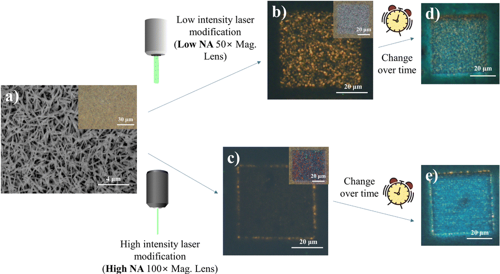 | ||
| Fig. 1 Schematic outline for laser-induced modification of In2O3 nanowire array. Variable optical and photoluminescence (PL) output induced by localized irradiation using a focused laser beam (532 nm CW) under different laser intensities modulated by lens numerical aperture (NA). (a) SEM layout of the pristine nanowire sample. (b and c) Fluorescence micrographs (FM; under UV excitation) of samples directly after laser modification with different laser intensities. (d and e) FM images showing a further transformation in PL presentation of the modified samples upon prolonged storage. Insets in (a–c) optical micrographs of the pristine vertical nanowire array, and the respective laser-processed regions under different laser intensities. | ||
Production and characterization: indium oxide (In2O3) nanowires
The vertical array of In2O3 nanowires was synthesized via a previously described low-RF plasma-assisted reactive evaporation protocol.27–30 Specifically, the adjusted parameters permitted a self-catalyzed growth process driven by molten droplets of In metal, in cooperation with the native oxide atop the silicon substrate to form the nanowires.31 Through RF generation of nitrogen plasma across the coil of tungsten filament which encloses an indium wire (Fig. S1a, ESI†), the procedure allowed for regulated control over various parameters to yield In2O3 of variable dimensions and qualities. More importantly, with the heat source filament isolated (∼1.5 cm above) away from the substrate, the technique allowed for the low substrate temperatures (200–300 °C) crucial for compatibility with other nano-characterization techniques or electronic post-processing. Herein, our samples were produced under optimized conditions of 200 W RF power and 300 °C substrate temperature.Under scrutiny by SEM, the nanowire morphology along with its dimensions were ascertained with lengths up to 4 μm and widths on the scale of 100 nm (Fig. S1b, ESI†). A concomitant EDX representation denotes the major composition of indium and oxygen in the nanowires, with minor silicon content due to the underlying substrate (Fig. S1c, ESI†). The uniformity of the nanowires and their homogeneous distribution were further ascertained by higher magnification SEM (Fig. S1b inset, ESI†) and optical microscopy (Fig. S1d, ESI†), respectively. The corresponding FM images (Fig. S1e and f, ESI†) under UV excitation revealed fairly weak fluorescence of the sample, with a faint hue of a green–yellow mixture discernible only at long exposures of 15 s. The corresponding PL spectrum (Fig. S1g, ESI†) denoted two distinct broad Gaussian regions centered at about 610 and 777 nm, both of which displayed close to linear correlation with laser power, indicative of bound excitonic recombination (Fig. S1g inset, ESI†). The composition of the nanowires was verified through corroborated outputs from Raman spectroscopy, EDX mappings, XPS and XRD analyses. The Raman results (Fig. S1h, ESI†) provided identifiable features comparable to those reported for In2O3 nanowires in the bcc cubic phase,32,33 with the exception of peaks at 250 cm−1 and 590 cm−1 typically attributed either to the nanostructure construction34,35 or to small quantities of the rhombohedral phase In2O3 (rh-In2O3, R![[3 with combining macron]](https://www.rsc.org/images/entities/char_0033_0304.gif) c).36–38 Compositional analysis with EDX mapping yielded uniform distributions of In and O in ratios (1
c).36–38 Compositional analysis with EDX mapping yielded uniform distributions of In and O in ratios (1![[thin space (1/6-em)]](https://www.rsc.org/images/entities/char_2009.gif) :1.58) (Fig. S1i–k, ESI†) similar to theoretical expectations (1:1.50). The XRD output (Fig. S1l, ESI†) confirmed that the sample was in the bixbyite phase (c-In2O3, Ia (206)) verified by JCPDS 65-3170 (Fig. S1l inset, ESI†),37,39 while analyses across HRTEM (Fig. S1m, ESI†) and SAED (Fig. S1m inset, ESI†) confirmed the high crystalline quality of the sample, with 0.18 nm interplanar spacing closely assigned to the (440) plane of cubic In2O3.40 Finally, the direct XPS output confirmed the chemical compositions of the nanowires, with In 3d (Fig. S1o, ESI†) and O 1s (Fig. S1q, ESI†) maps dominant in In2O3 signals incorporating a hydroxide surface (In(OH)3) and meagre quantities of oxygen vacancy (VO)-related species.41–43 With C 1s (Fig. S1n, ESI†) and N 1s (Fig. S1p, ESI†) analyses, minute amounts of carbon-based absorbates and interstitial nitrogen inclusions44 were identified, along with possible components of InN.45,46
:1.58) (Fig. S1i–k, ESI†) similar to theoretical expectations (1:1.50). The XRD output (Fig. S1l, ESI†) confirmed that the sample was in the bixbyite phase (c-In2O3, Ia (206)) verified by JCPDS 65-3170 (Fig. S1l inset, ESI†),37,39 while analyses across HRTEM (Fig. S1m, ESI†) and SAED (Fig. S1m inset, ESI†) confirmed the high crystalline quality of the sample, with 0.18 nm interplanar spacing closely assigned to the (440) plane of cubic In2O3.40 Finally, the direct XPS output confirmed the chemical compositions of the nanowires, with In 3d (Fig. S1o, ESI†) and O 1s (Fig. S1q, ESI†) maps dominant in In2O3 signals incorporating a hydroxide surface (In(OH)3) and meagre quantities of oxygen vacancy (VO)-related species.41–43 With C 1s (Fig. S1n, ESI†) and N 1s (Fig. S1p, ESI†) analyses, minute amounts of carbon-based absorbates and interstitial nitrogen inclusions44 were identified, along with possible components of InN.45,46
Laser-induced modification of nanowire optical properties
Through a series of optical mirrors, the beam path of a 532 nm laser was directed through a back aperture of the metallurgical microscope unit. The laser travels a route identical to that of the optical light path, before it gets deflected by the dichroic mirror of the filter unit and is focused through the objective lens upon the sample surface. Herein, a micro-stage controller allows precise control of the programmed lateral movements along the stage, while a back-reflecting shutter unit quickly shutters the laser on/off, both contributing to precise manipulation of the laser raster area and pattern. The flexibility to adapt a homemade gas chamber atop the microscope stage, with air-sealed connections to a vacuum pump and gas tank inlet, allows for the same laser raster operations amidst regulated gas environments with the sample placed within, and the holder topped with a quartz crystal (Fig. 2a).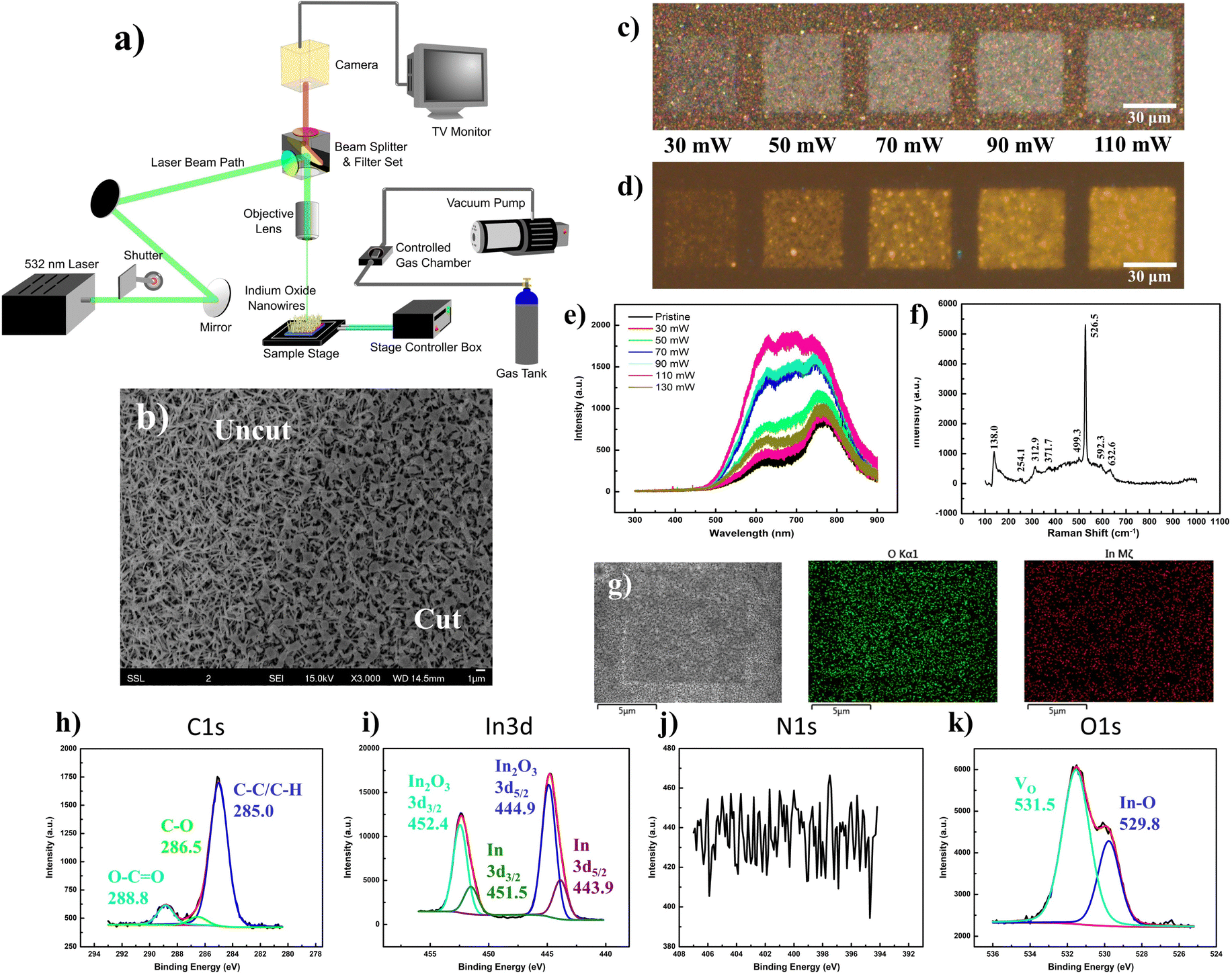 | ||
| Fig. 2 Laser modification of In2O3 nanowire array under ambient conditions: yellow fluorescence. (a) Schematic layout of focused laser microscope setup tethered with a 532 nm laser beam input and micro-stage controller. Homemade gas environment chamber (with vacuum and variable gas tank inlet) available as an attachment for environment-controlled laser modification. (b) SEM analysis at the periphery of the square region altered at low laser intensity (50 mW, low lens NA), demonstrating the change in morphology at the “cut–uncut” interface. (c) OM bright field image of laser-modified region, along with (d) corresponding FM images (under UV light excitation) across a range of laser powers. (e) PL spectrum profile (325 nm UV excitation) of laser-modified nanowire region under variable irradiation powers, demonstrating the evolution of a broad multipeak signal after laser modification at different powers in the range 70–110 mW, consistent with the acquired bright yellow luminescence in (d). (f) Acquired Raman spectrum of laser-modified nanowire region under 532 nm excitation. (g) SEM-EDX analysis for a typical low-intensity laser-modified square under 50 mW laser power: low-magnification SEM image with corresponding O Kα and In Mζ maps. (h–k) XPS spectra of the laser-modified regions, presenting elemental signals of (h) C 1s, (i) In 3d (j) N 1s (k) O 1s. | ||
Under the influence of the laser focused through a low-magnification objective (low NA), the nanowires conform to a slightly melted state (Fig. 2b), particularly at the intersection of the overlying topmost nanowires. Surprisingly, this seemingly minor change in morphology reflects a more dramatic change in the optical appearance of the nanowire array, transforming it from a yellowish spotted mesh to a greyish-white “crystalline-like” form (Fig. 2c). Across a power range of 70–110 mW, the modified region emits a bright yellow fluorescence (Fig. 2d) relative to the dark background, with a severely broadened PL emission profile ranging from 500 nm to beyond 800 nm (Fig. 2e). Herein, it is expected that the laser incorporation of ambient oxygen into the bixbyite lattice may have replenished any oxygen vacancy sites, prompting an optical contrast47 relating to the larger bandgap (>2.9 eV)48–50 of In2O3 in accurate stoichiometries, while any laser thermal influence prompted an improved sample crystallinity. The integration of excessive oxygen content would further prompt various defects, such as Oi, OIn or composite defects coupled between the interstitial element with remnant vacancies, giving a complex PL plateau from the merger of mixed emission profiles. Deconvoluted into its multiple Gaussian components, the broad PL profile of the yellow emission was fitted by up to seven components stemming from a complex interplay between the defect contributions (Fig. S2, ESI†). In contrast, laser modifications made at lower (≤30 mW, low lens NA) and higher (130 mW, low lens NA) laser powers demonstrated much weaker emissions with a deconstructed PL profile analogous to that of the pristine sample.
With Raman characterization, the laser-modified region was found to retain most of the vibration modes associated with In2O3 species (Fig. 2f). Notably, the laser-modification process brought about a decrease in peak intensity at 254 cm−1, compensated by an increase at 312 cm−1. Herein, it would be reasonable that the morphological “melting” accounts for the decrease in any rhombohedral phase or nanowire-related vibrations. In contrast, the increase in magnitude of the νIn–O–In (stretching) vibration at 312 cm−1 could easily be explained by the passivation of ambient oxygen at vacancy sites. The notion of oxygen incorporation was further corroborated by SEM-EDX mappings (Fig. 2g), where the map of oxygen distribution (O Kα) distinctly displays a square region of enhanced counts identical to the laser-modified pattern. Under the scrutiny of the XPS instrumentation (Fig. 2h–k), the laser-effected changes were found predominantly in the removal of surface InN and In(OH)3 components, together with the revelation of underlying In species.
To verify the hypothesized impact of laser-incorporated oxygen on the acquired fluorescence, comparative low-intensity (low lens NA) laser alterations were conducted for the same sample placed within controlled oxygen and vacuum conditions. As anticipated, the regions laser-processed under the oxygen-rich environment (across a range of laser powers (20 mW, 50 mW, 90 mW)) were endowed with lighter optical hues (Fig. 3a), accompanied by yellow fluorescence (Fig. 3b) brighter than regions processed under ambient conditions (Fig. 2d). In contrast, vacuum conditions produced darker, slightly deeper “sink-in” domains with much weaker emission (Fig. 3c and d). It is expected that the lack of endothermic oxidation in the sample under vacuum conditions forces a greater degree of localized heating to cause more extensive sample damage. Examined under SEM, the morphological changes were akin to those of the ambient modified samples and generally involve nanowires melted at the conjoined or interconnected points (Fig. 3e and f). Such similarities would dispel suspicions of a fluorescence discrepancy arising from major variations in the nano-morphologies of the respective sample regions. Finally, when overlaid upon a single plot, the PL layout (Fig. 3g) for a sample laser-modified in oxygen demonstrated enhanced emission intensity relative to that under ambient conditions, while those of samples modified in oxygen-free conditions (vacuum or helium) were more equivalent in profile to an unmodified sample. This confirmed the critical correlation of oxygen concentration in the surrounding vicinity with the brilliance of the acquired yellow fluorescence.
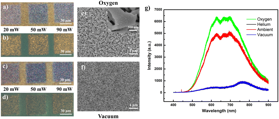 | ||
| Fig. 3 Low-intensity (low lens NA) laser modification of In2O3 nanowires under environmental control. (a) OM of sample laser modified under an oxygen-filled environment with its associated (b) FM landscape. (c) OM of sample laser-modified under vacuum conditions with its associated (d) FM landscape. (e) Corresponding SEM image for sample modified (50 mW) in oxygen. (f) Corresponding SEM morphology for sample laser-modified (50 mW) in a vacuum. (g) Comparison of PL emission profile for samples laser-modified under the different set conditions. The sample modified in a helium environment was found to adopt an overlapping PL profile against that modified in a vacuum. | ||
Furthermore, the reproducibility of the laser-transformation phenomena was also ascertained in multiple repeated runs with slight variations across the key parameters (Fig. S3, ESI†). The impact of the incident laser power was found to be greater in comparison to the laser raster speed. While the optical contrast (Fig. S3a, ESI†) and fluorescence (Fig. S3b, ESI†) remained fairly consistent across the range of raster speeds (10–60 μm s−1), the change in laser power (20–80 mW) induced a gradual optical transition from the whitish “crystalline” form to a greyish state. With increasing laser power, the sample also presents gradually diminishing fluorescence intensities and the formation of fluorescing perimeter rims. As the decreased raster speed is expected to prolong the holding duration of the laser spot at each point within the raster region and thus increase the localized heating influence analogous to a smaller increment in laser intensity, the raster speed could potentially be a more refined parameter for evaluating the laser-induced changes.
Comparatively, the XPS details across the pristine and laser-modified samples also deliver insights into the changes associated with the laser processes. In particular, the evolution in indium and nitrogen-based compounds across the laser thinning process prompted a schematic model (Fig. 4a) supplemented by HRTEM analyses. Obtained through a self-catalyzed growth process mediated by directional oxidation at the surface of the molten indium droplets, the obtained nanowires typically include a nanoparticle (Fig. 4b) at the far-end tip confirmed by SAED to be composed purely of remnant indium (Fig. 4c and inset). In other instances, sparse inclusions of InN were similarly identified by SAED in a non-homogeneous distribution close to the nanowire apex (Fig. 4d and e and inset). Correlating with the XPS findings, it is possible that longer strands of nanowires that emerge beyond the surface nanowire canopy would have their indium catalyst oxidized to In2O3 or In(OH)3, owing to extended exposure to the ambient surroundings. The analyzed area of the pristine sample happens to have sampled nanowires containing the InN component. Upon laser removal of the topmost layer inclusive of InN and In(OH)3, the underlying mid-layer mixture of half-cut nanowires and unexposed shorter nanowires that still carry pristine indium nanoparticles is now exposed, accounting for the newfound signals in the XPS results. Through sideview SEM imaging, the sample modified by low laser intensity revealed a sink-in of 2.42 μm (Fig. 4f) at the cut–uncut interface, marked by the peripheral standing nanowires (Fig. 4g), in stark contrast to the deeper 4.73 μm (Fig. 4h) under higher intensity irradiation. Furthermore, under the scrutiny of TEM EDX analysis (Fig. S4a, ESI†) at the nanowire tip region, distinct signals of In, N and O were acquired (Fig. S4b–e, ESI†). The results not only substantiated the presence of InN species at the nanowire apex, but also described a non-stoichiometric excess of In in the region, reiterating the possibility of embedded indium nanoparticles (Fig. S4f, ESI†).
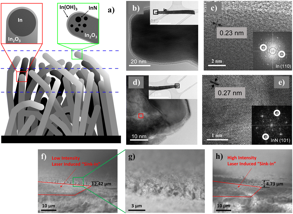 | ||
| Fig. 4 Evaluation of nanowire depth profile and distribution of elemental species. (a) Schematics of standing nanowire cross-section and distribution of indium-related composition. (b) HRTEM of a single representative nanowire tip. (c) Higher magnification HRTEM demonstrating the inclusion of an In nanoparticle catalyst at the tip of the nanowire. Inset: SAED patterns identifying the pure In component in the selected scan region. (d) HRTEM of another representative nanowire tip (e) magnified HRTEM of region marked by red box in (d), demonstrating the non-homogeneous distribution of InN clusters at the nanowire tip. Inset: SAED patterns identifying the InN components. (f) Side-view cross-sectional SEM of sample under low-intensity (low lens NA) laser engineering. (g) Zoom-in cross-section at interface of cut–uncut region showing depth of 2.42 μm. (h) Similar side-view SEM profile under high laser (high lens NA) intensity, scaling a depth of approximately 4.73 μm. | ||
Laser-induced changes – post laser environmental influences
Upon prolonged storage and gas exposure, the samples demonstrated distinct transformation in their fluorescence profiles. Under low-intensity laser modification, the typical crystalline optical (Fig. 5a) and yellow fluorescent (Fig. 5b) laser-modified regions were initially obtained. While the optical appearance remained consistent over extended placement in an ambient environment, the fluorescence landscape was topped with a confounding layer of bluish-green hue that gradually appeared upon the modified sample surface (Fig. 5c). The associated Raman spectrum reveals a further decline in the signal at 254 cm−1 (Fig. 5d), coherent with the SEM characterization that reveals the loss of nanowire morphology as domains of spiked bumps emerge (Fig. 5e).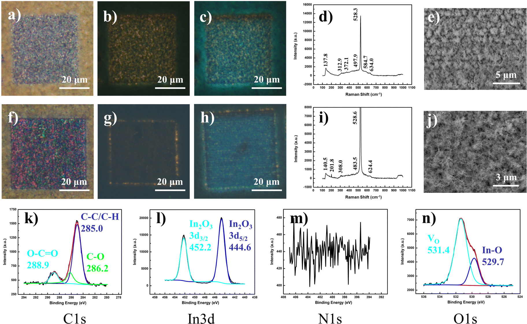 | ||
| Fig. 5 Post-modification fluorescence changes under various surrounding conditions: blue fluorescence. (a) OM of nanowire domain modified with low-intensity (low lens NA) laser exposure, with its corresponding (b) FM image. (c) FM image of laser-modified region in (a) and (b) evolved after prolonged storage under ambient conditions. (d) Raman profile and (e) SEM display for sample after storage changes (in (c)). (f) OM of nanowire domain modified with high-intensity (high lens NA) laser exposure, with corresponding (g) FM image. (h) FM image of laser-modified region in (f) and (g) evolved after prolonged storage under ambient conditions. (i) Raman profile and (j) SEM display for sample after storage changes in (h). (k–n) XPS analyses for typical sample in (h) of elemental compositions (k) C 1s (l) In 3d (m) N 1s (n) O 1s. | ||
In contrast, samples modified with high-intensity (high lens NA) lasers are characterized by an optical appearance that comprises a multicolored mix of predominantly pink and green hues (Fig. 5f), along with an FM image demarcated by a perimeter of yellow fluorescence encompassing a central area of similar but weaker emission (Fig. 5g). With such an energetic range of irradiation intensities, the laser influence transcends the comfortable range for optimal defect-induced fluorescence, presenting a severe decline due to sample damage; only with weakened remnant laser intensity at the radial beam waist was fluorescence achieved. The corresponding evolution under ambient storage was similar, with the optical image retaining its original look, while the fluorescence profile adopts an added coat of turquoise in the laser-modified region (Fig. 5h). A similar Raman spectrum was acquired, with the lack of nanowire features (254 cm−1) while maintaining characteristic signals for νIn–O–In (stretching; 308 cm−1) and νbcc (In2O3; 483.5 cm−1, 624.4 cm−1) (Fig. 5i). Under SEM analysis, a new morphology was observed, consisting of much finer nanofibers entangled in a dense mesh (Fig. 5j). With analysis of the “blue” transformed state of the modified region, the XPS results (Fig. 5k–n) afforded signals distinctive of a pure In2O3 composition, without contributions from other indium-based compounds (In(OH)3, In, InN) at this laser-induced depth.
In a comparison between samples modified with varying laser intensities under ambient conditions, the rate of fluorescence change was found to correlate with nanostructure morphology. While samples modified under high laser intensities were found to produce the overlying turquoise emission over the course of a day, samples from the low-intensity process took up to a week for discernible blue contributions. Hypothesized to involve a surface molecular adsorption process, we thus expect the large surface area owing to the nano-fibrous morphology to favor greater adsorption kinetics in comparison to that of spiked cluster domains. Furthermore, a similar morphology-to-fluorescence relation was also observed for the sample modified by a high-intensity laser under varied environmental conditions. Across laser alterations performed under ambient (Fig. S5a–d, ESI†), oxygen-rich (Fig. S5e–h, ESI†) and vacuum (Fig. S5i–l, ESI†) conditions, the nano-morphologies adopted a trend of decreasing surface to area ratio stemming from the corresponding nano-fibrous network (Fig. S5d, ESI†), fibrous clusters (Fig. S5h, ESI†) and melted particle mix (Fig. S5l, ESI†). In a similar fashion, the rate of fluorescence transformation, in which the bluish contribution can be discernible, was found to concur in the order of ambient > oxygen > vacuum. More intriguingly, the samples modified under vacuum conditions were found to be severely compromised in their fluorescence properties, with almost none of the yellow fluorescence features that never turned blue. With the lack of endothermic oxidative or crystal transformation reactions under vacuum conditions, the accumulation of localized laser energy is expected to always bring about strong thermal conditions that may have destroyed the material of any indium oxide form capable of sustaining its fluorescent properties. Furthermore, this marks an assurance that the established phenomenon does not involve any interference from the underlying silicon substrate exposed under high-intensity laser irradiation.
In further evaluation of the fluorescence changing process, the idea of surface absorption was evaluated by adsorption–desorption under various perturbations. To begin with, the distribution of the various yellow and blue emitting regions was analyzed along the vertical z-axis by varying the FM z-focus. Mapped in correlation with the optical image (Fig. S6a, ESI†), the topmost imaging focused upon peripheral unaltered nanowire array domains (Fig. S6b, ESI†). Moving downwards within the “sunk-in” modified region, the fluorescence image first focuses onto the utmost layer of blue fluorescence spots (Fig. S6c, ESI†), before subsequent focusing upon the underlying yellow fluorescing regions (Fig. S6d, ESI†). The vertical distance between the focal planes for the respective fluorescence regions was measured through a calibrated scale on the microscope z-axis, yielding an estimated 3 μm for the thickness of the blue fluorescing domain. With UV exposure under continual fluorescence imaging, the surface layer of blue was gradually dispelled (Fig. 6 and Fig. S7, ESI†), transiting various states of turquoise (Fig. 6c and d) and green emission (Fig. 6e–h) before reverting to the original yellow emitting state (Fig. 6j) upon extended UV exposure. Surprisingly, with the subsequent removal of the UV source, the fluorescence transformation and recovery of the blue component commenced instantaneously and was discernible within a short time range of 1.5 hours (Fig. 6k and l). With the changes being highly reproducible and easily achievable for samples modified under both high- and low-intensity lasers (Fig. 6 and Fig. S7, ESI†), the fluorescence transformation dynamics hinted at a surface absorption–desorption process universal to the modified sample variants. Furthermore, with thermal annealing in an ambient setting, a similar desorption of surface absorbates was also achieved (Fig. S8, ESI†), thinning out the overlaying blue contributions in the recovery of the original yellow-emitting (low-intensity-modified) and yellow-edge-emitting (high-intensity-modified) states. As such, the system not only prompts the potential for recovery to the original state, but also provides dynamic accessibility across the wide range of intermediate emitting states through the broad parameter of UV exposure time.
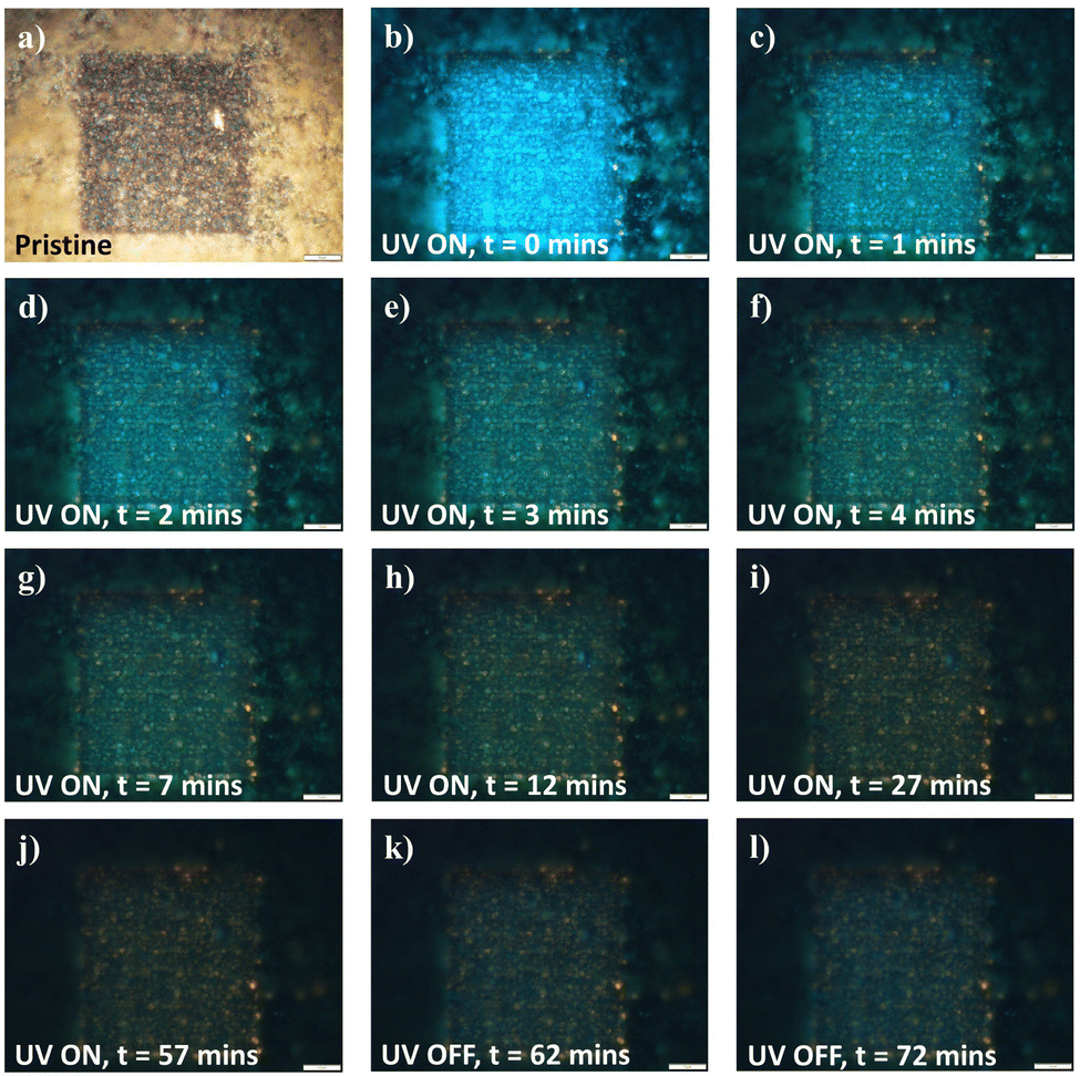 | ||
| Fig. 6 Sample fluorescence evolution under time-varied UV exposure ON–OFF. (a) OM layout of low-intensity (low lens NA) sample laser-modified region after prolonged ambient exposure. (b–j) Corresponding time points across UV exposure duration and influence on sample fluorescence: (b) t = 0 min, (c) t = 1 min, (d) t = 2 min, (e) t = 3 min, (f) t = 4 min, (g) t = 7 min, (h) t = 12 min, (i) t = 27 min, (j) t = 57 min, demonstrating a decreasing blue component with increased UV exposure time. (k and l) Corresponding time points after cut-off of UV exposure and effect on sample fluorescence: (k) t = 62 min, (l) t = 72 min, demonstrating the recovery of the blue fluorescence component. | ||
Laser induced changes – reference controls
In order to understand the mechanics behind the absorption-induced fluorescence conversion, it is imperative to evaluate the sample's response under various environmental controls to narrow down the exact molecular system responsible for the change. Based upon atmospheric composition, samples with fresh laser modifications were separately stored under nitrogen, oxygen, carbon dioxide and high-humidity conditions to invoke the observed fluorescence transformation. Stored under oxygen-rich conditions (Fig. S9a and d, ESI†), the sample was found to develop gradual brightening of both yellow and blue fluorescence within the laser-modified area. Comparatively, the fluorescence profile pertaining to samples stored under carbon dioxide (Fig. S9b and e, ESI†) or nitrogen (Fig. S9c and f, ESI†) environments stayed invariant over the period of gaseous exposure.Given that the storage conditions involved a humid ambient climate, any latent influence of water content on the changes in PL should be well-accounted for. Ambient laser-modified samples processed under various laser intensities were treated in a high-humidity closed chamber. Presented in Fig. S10a and b (ESI†), sustained exposure for both samples did not show any discernible blue emission across the five-hour experimental window; any background influence from water adsorption can effectively be eliminated.
Fluorescence mechanism
Given that stoichiometric In2O3 possesses an inherently wide bandgap (3.0–3.4 eV; Fig. 7a), a multitude of electronic transitions with lower energies (1.7–2.1 eV) embedded within the yellow fluorescence is expected to arise from defect states situated within the gap, characterized by the typical broad-band emission encompassing contributions from various defect state transitions. With oxygen content mediating an enhancement in the yellow emission acquired, it becomes intuitive to assign oxygen-related defects (Oi, OIn, (Oi–VO)) involving deep acceptor states positioned mid-gap for these low-energy emissions (Fig. 7b).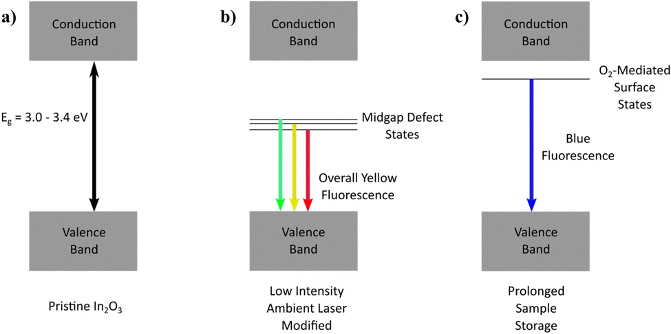 | ||
| Fig. 7 Illustration of energy level profile for various fluorescence mechanisms. (a) Energy level profile for pristine full stoichiometric In2O3 demonstrating a wide bandgap of 3.0–3.4 eV. (b) Energy level distribution for In2O3 sample (low-intensity) laser-modified under ambient conditions, demonstrating the broad-range multi-transition emission from deep acceptor defect states. (c) Prolonged sample storage after ambient laser-modification, illustrating the surface layer blue emission originating from surface-adsorbed oxygen molecules. | ||
Besides the laser-assisted generation of bright yellow emission due to oxygen atoms incorporated in the crystal matrix (filling vacancies, interstitial sites, chemisorption), the oxygen molecules were found to also contribute to the time-dependent blue fluorescence acquired from physical adsorption upon the lasered sample surface. Since the top-layer blue emission was found to be inducible only with oxygen exposure, and reversible under UV irradiation or thermal treatment, the process was hypothesized to involve surface states of a shallow donor nature (Fig. 7c). Depending on the position of the molecular electronic states relative to the In2O3 Fermi level, charge transfer dynamics may also make a contribution to the emission process.51
Application – micropatterning and anti-counterfeiting technology
To demonstrate the flexibility and control of the laser-modification technique to dictate In2O3 nanowire PL down to the micron scale, a proof of concept was performed to derive micropatterns of differing states. Simply through modulation in laser intensity, spatially refined micropatterns of disparate optical (Fig. 8a and c) and fluorescent (Fig. 8b and d) appearances were attained. With the potential for a blue overcoat upon selective gas exposure treatment and storage, accessibility across the various “yellow” and “blue” emitting states offers region-selective dual-color fluorescence for high-resolution micro-displays and anti-counterfeiting embeddings.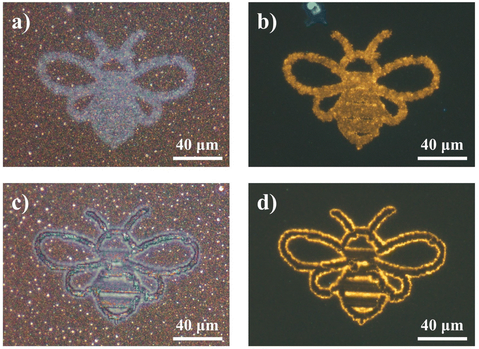 | ||
| Fig. 8 Laser-controlled micropatterning. (a) OM image of “bee” micropattern demonstrated with low-intensity (low lens NA) laser-modification, along with corresponding (b) FM image. (c) OM image of “bee” micropattern demonstrated with high-intensity (high lens NA) laser-modification, along with corresponding (d) FM image. | ||
Furthermore, with the transitional feature of the blue fluorescence component under UV readout lies an additional dynamic layer of heightened security trait hidden beneath the unaltered bright field optical contrast of the sample. The multilayer encryption begins with the micropattern readout under bright field and fluorescence modes (Fig. 9a), before the next-level assurance through a distinctive blue–green–yellow transition arising from dissipation of the overlayer blue emission, discernible in the time order of seconds to minutes (Fig. 9b). For advanced security detailing, a third level of sample encoding can be applied across the time domain, by assigning screenshots of the varying sample PL states to timepoint values in a pre-established database for comparative verification, or through a pre-recorded intensity to time correlation of the PL transformation process for a quantitative comparison (Fig. 9c). Together, these various encryption checkpoints consolidated within a single complex micropattern assure optimal anti-counterfeiting and security authentication. Only with all features coherently present at high accuracy within a specimen can the authenticity be validated.
 | ||
| Fig. 9 Proposed multilayer complex security anti-counterfeiting application. (a) Schematics of dual-color fluorescence micropatterns embedded within a passport illustration. (b) Additional layer of security detail from dynamic fluorescence evolution coming from gradual dissipation of surface blue emission. (c) Further encryption from time-domain fluorescence encoding and features. | ||
Capitalizing upon the time-reversibility in the sample's incessant and gradual evolution in fluorescence, the optical readout could easily be reused over multiple runs. With the increasing involvement of artificial intelligence and machine–learning platforms in anti-counterfeiting readouts, improved verification procedures with better precision can be developed. Furthermore, the time-dependent change in fluorescence color is expected to provide value in reusable time-sensitive packaging or optical expiry label tagging for quickly perishable items. With an understanding of the time required for a full color change process, the label could be assigned as fixed time markers for items predicted to expire within the assigned timeframes and would be especially useful for items involving oxygen-liberating processes. Also, since the adsorption–desorption process was found to be reliant upon UV exposure intensity, along with oxygen concentration, the system could potentially be applicable for oxygen sensing and UV exposure (time and intensity) calibration purposes as well.
Conclusions
In summary, we have reported the initiation of various fluorescence features through laser-induced surface modification upon a standing array of indium oxide nanowires. With laser incorporation of oxygen species amid the sample lattice, a newfound yellow emission was first achieved, before a subsequent blue fluorescence overlayer was obtained from surface oxygen physisorption upon prolonged storage. The respective emissions were reasoned to originate from the addition of deep defect and shallow surface states within the wide-bandgap host nanomaterial. Exploiting the volatile non-steady-state dynamics of the blue fluorescence adsorption–desorption under UV exposure, we developed a system of multi-dimensional anti-counterfeiting capability through multilayer verification checkpoints of microscale patterning, dynamic color evolution and time-domain encoding.Experimental section
Material characterization
Sample bright field OM and FM images were captured using an Olympus BX51 upright microscope coupled with an LED top illuminator and an appropriate set of filters. Raman and PL spectra were acquired from a Renishaw inVia 2000 Micro-Raman system using the respective 532 nm and 325 nm excitation lines. The SEM images and corresponding energy dispersive X-ray (EDX) maps were obtained from a JEOL JSM-6700F field emission scanning electron microscope (FESEM) operated at 15 kV, coupled with an Oxford Instruments X-MaxN 150 EDX detector. TEM and HRTEM details were acquired using a JEOL 2010 HRTEM, with the samples prepared on carbon-coated copper grids (Lacey 300 mesh Cu). Sample XRD diffractograms were measured using a PANalytical Empyrean X-ray diffractometer operating at 1.5406 Å with fixed grazing incidence angle of 0.5° across a 2θ range of 20°–80°. Sample scan step time and step size were fixed at 2.0 s and 0.026°, respectively. XPS elemental analyses were conducted on a Thermo Fisher Scientific Theta Probe XPS system.Author contributions
The project was conducted under the supervision and advice from Boon Tong Goh and Chorng Haur Sow. Eng Tuan Poh designed and planned the project, experiments, and manuscript structure. Yung Zhen Tan, Justin Boon Shuan Neo, Chee How Ong, and Jianhui Li carried out the experiments, characterization, and data analyses under the guidance of Eng Tuan Poh. Azianty Saroni contributed to the pristine nanowire growth while Zheng Zhang provided the XPS characterization and analysis. All authors discussed the results and reviewed the manuscript drafts.Conflicts of interest
There are no conflicts to declare.Acknowledgements
E. T. Poh and C. H. Sow acknowledge the generous support from the NUS Resilience & Growth Postdoctoral Fellowship (R-144-000-471-281/A-0000065-65-00). This collaboration effort was part of the Temasek Foundation International – NUS STEM Programme for University Educators in ASEAN.Notes and references
- A. Galdámez-Martinez, G. Santana, F. Güell, P. R. Martínez-Alanis and A. Dutt, Nanomaterials, 2020, 10, 857 CrossRef PubMed.
- F. Kayaci, S. Vempati, I. Donmez, N. Biyikli and T. Uyar, Nanoscale, 2014, 6, 10224–10234 RSC.
- J. Zhou, K. Nomenyo, C. C. Cesar, A. Lusson, A. Schwartzberg, C. C. Yen, W. Y. Woon and G. Lerondel, Sci. Rep., 2020, 10, 4237 CrossRef CAS PubMed.
- A. Bah, K. Y. Lim, F. Wei, A. Khursheed and C. H. Sow, Sci. Rep., 2019, 9, 9671 CrossRef PubMed.
- M. D. McCluskey and S. J. Jokela, J. Appl. Phys., 2009, 106, 071101 CrossRef.
- D. Wang and N. Reynolds, ISRN Condens. Matter Phys., 2012, 2012, 950354 Search PubMed.
- S. Sun, G. Meng, G. Zhang, J. P. Masse and L. Zhang, Chem. – Eur. J., 2007, 13, 9087–9092 CrossRef CAS PubMed.
- A. Kar, M. A. Stroscio, M. Dutta, J. Kumari and M. Meyyappan, 2009 IEEE Nanotechnol. Mater. Devices Conf. NMDC 2009, 2009, 121–125 CAS.
- B. Liu, C. W. Cheng, R. Chen, Z. X. Shen, H. J. Fan and H. D. Sun, J. Phys. Chem. C, 2010, 114, 3407–3410 CrossRef CAS.
- M. Bhatnagar, V. Kaushik, A. Kaushal, M. Singh and B. R. Mehta, AIP Adv., 2016, 6, 095321 CrossRef.
- F. Gu, S. F. Wang and M. K. Lu, J. Phys. Chem. B, 2004, 108, 8119–8123 CrossRef CAS.
- J. D. Prades, J. Arbiol, A. Cirera, J. R. Morante, M. Avella, L. Zanotti, E. Comini, G. Faglia and G. Sberveglieri, Sens. Actuators, B, 2007, 126, 6–12 CrossRef CAS.
- Y. Lu, J. Zhao, R. Zhang, Y. Liu, D. Liu, E. M. Goldys, X. Yang, P. Xi, A. Sunna, J. Lu, Y. Shi, R. C. Leif, Y. Huo, J. Shen, J. A. Piper, J. P. Robinson and D. Jin, Nat. Photonics, 2014, 8, 32–36 CrossRef CAS.
- X. Liu, Y. Wang, X. Li, Z. Yi, R. Deng, L. Liang, X. Xie, D. T. B. Loong, S. Song, D. Fan, A. H. All, H. Zhang, L. Huang and X. Liu, Nat. Commun., 2017, 8, 899 CrossRef PubMed.
- Y. Liu, F. Han, F. Li, Y. Zhao, M. Chen, Z. Xu, X. Zheng, H. Hu, J. Yao, T. Guo, W. Lin, Y. Zheng, B. You, P. Liu, Y. Li and L. Qian, Nat. Commun., 2019, 10, 2409 CrossRef PubMed.
- W. Ren, G. Lin, C. Clarke, J. Zhou and D. Jin, Adv. Mater., 2020, 32, 1901430 CrossRef CAS PubMed.
- H. F. Teoh, P. Dzung, W. Q. Lim, J. H. Chua, K. K. Lee, Z. Hu, H. Tan, E. S. Tok and C. H. Sow, Nanoscale, 2014, 6, 3143–3149 RSC.
- E. T. Poh, X. Liu and C. H. Sow, Adv. Mater. Interfaces, 2019, 6, 1901673 CrossRef CAS.
- F. C. Cheong, B. Varghese, S. Sindhu, C. M. Liu, S. Valiyaveettil, A. A. Bettiol, J. A. Van Kan, F. Watt, W. S. Chin, C. T. Lim and C. H. Sow, Appl. Phys. A: Mater. Sci. Process., 2007, 87, 71–76 CrossRef CAS.
- K. Y. Lim, C. H. Sow, J. Lin, F. C. Cheong, Z. X. Shen, J. T. L. Thong, K. C. Chin and A. T. S. W. Wee, Adv. Mater., 2003, 15, 300–303 CrossRef CAS.
- X. Lim, Y. Zhu, F. C. Cheong, N. M. Hanafiah, S. Valiyaveettil and C. H. Sow, ACS Nano, 2008, 2, 1389–1395 CrossRef CAS PubMed.
- J. Gupta, X. Lim, C.-H. Sow and C. Vijayan, J. Nanosci. Nanotechnol., 2011, 11, 4029–4033 CrossRef CAS PubMed.
- Y. R. Choi, M. Zheng, F. Bai, J. Liu, E. S. Tok, Z. Huang and C. H. Sow, Sci. Rep., 2014, 4, 4940 CrossRef PubMed.
- J. Lu, J. H. Lu, H. Liu, B. Liu, L. Gong, E. S. Tok, K. P. Loh and C. H. Sow, Small, 2015, 11, 1792–1800 CrossRef CAS PubMed.
- A. Venkatakrishnan, H. Chua, P. Tan, Z. Hu, H. Liu, Y. Liu, A. Carvalho, J. Lu and C. H. Sow, ACS Nano, 2017, 11, 713–720 CrossRef CAS PubMed.
- S. X. Lim, Y. Z. Lee, N. Gao, J. Lu, Q. Xu, E. S. Tok and C. H. Sow, J. Mater. Chem. C, 2018, 6, 4641–4648 RSC.
- M. Alizadeh, B. T. Goh, A. K. Pandey, C. F. Dee and S. A. Rahman, Mater. Chem. Phys., 2017, 199, 408–415 CrossRef CAS.
- A. Saroni, M. Alizadeh, S. A. Rahman, C. F. Dee and B. T. Goh, Mater. Sci. Semicond. Process., 2017, 68, 6–14 CrossRef CAS.
- A. Saroni, M. Alizadeh, S. A. Rahman, W. Meevasana and B. T. Goh, J. Power Sources, 2020, 480, 228829 CrossRef CAS.
- V. Ganesh, M. Alizadeh, A. Shuhaimi, A. Pandikumar, B. T. Goh, N. M. Huang and S. A. Rahman, RSC Adv., 2015, 5, 17325–17335 RSC.
- A. B. Saroni, PhD dissertation, University of Malaya, Kuala Lumpur, Malaysia, 2018.
- A. Shanmugasundaram, B. Ramireddy, P. Basak, S. V. Manorama and S. Srinath, J. Phys. Chem. C, 2014, 118, 6909–6921 CrossRef CAS.
- C. Kranert, R. Schmidt-Grund and M. Grundmann, Phys. Status Solidi – Rapid Res. Lett., 2014, 8, 554–559 CrossRef CAS.
- H. S. Kim, H. G. Na, J. C. Yang, C. Lee and H. W. Kim, Acta Phys. Pol., A, 2011, 119, 143–145 CrossRef CAS.
- X. S. Peng, Y. W. Wang, J. Zhang, X. F. Wang, L. X. Zhao, G. W. Meng and L. D. Zhang, Appl. Phys. A: Mater. Sci. Process., 2002, 74, 437–439 CrossRef CAS.
- C. Y. Wang, Y. Dai, J. Pezoldt, B. Lu, T. Kups, V. Cimalla and O. Ambacher, Cryst. Growth Des., 2008, 8, 1257–1260 CrossRef CAS.
- D. Liu, W. Lei, S. Qin, L. Hou, Z. Liu, Q. Cui and Y. Chen, J. Mater. Chem. A, 2013, 1, 5274–5278 RSC.
- L. Gai, L. Ma, H. Jiang, Y. Ma, Y. Tian and H. Liu, CrystEngComm, 2012, 14, 7479–7486 RSC.
- G. Zhu, L. Guo, X. Shen, Z. Ji, K. Chen and H. Zhou, Sens. Actuators, B, 2015, 220, 977–985 CrossRef CAS.
- X. Liu, L. Jiang, X. Jiang, X. Tian, X. Sun, Y. Wang, W. He, P. Hou, X. Deng and X. Xu, Appl. Surf. Sci., 2018, 428, 478–484 CrossRef CAS.
- K. K. Banger, Y. Yamashita, K. Mori, R. L. Peterson, T. Leedham, J. Rickard and H. Sirringhaus, Nat. Mater., 2011, 10, 45–50 CrossRef CAS PubMed.
- J. Y. Y. Loh and N. P. Kherani, Molecules, 2019, 24, 3818 CrossRef CAS PubMed.
- L. B. Hoch, T. E. Wood, P. G. O’Brien, K. Liao, L. M. Reyes, C. A. Mims and G. A. Ozin, Adv. Sci., 2014, 1, 1400013 CrossRef PubMed.
- W. Yin, D. V. Esposito, S. Yang, C. Ni, J. G. Chen, G. Zhao, Z. Zhang, C. Hu, M. Cao and B. Wei, J. Phys. Chem. C, 2010, 114, 13234–13240 CrossRef CAS.
- K. S. A. Butcher, A. J. Fernandes, P. P. T. Chen, M. Wintrebert-Fouquet, H. Timmers, S. K. Shrestha, H. Hirshy, R. M. Perks and B. F. Usher, J. Appl. Phys., 2007, 101, 123702 CrossRef.
- M. Alizadeh, B. T. Goh, K. Wasman Qadir, H. Yousefi, M. S. Mehmood and R. Rasuli, J. Mater. Sci.: Mater. Electron., 2019, 30, 15534–15543 CrossRef CAS.
- L. Wang, Y. Dong, T. Yan, Z. Hu, A. A. Jelle, D. M. Meira, P. N. Duchesne, J. Y. Y. Loh, C. Qiu, E. E. Storey, Y. Xu, W. Sun, M. Ghoussoub, N. P. Kherani, A. S. Helmy and G. A. Ozin, Nat. Commun., 2020, 11, 2432 CrossRef CAS PubMed.
- P. D. C. King, T. D. Veal, F. Fuchs, C. Y. Wang, D. J. Payne, A. Bourlange, H. Zhang, G. R. Bell, V. Cimalla, O. Ambacher, R. G. Egdell, F. Bechstedt and C. F. McConville, Phys. Rev. B: Condens. Matter Mater. Phys., 2009, 79, 205211 CrossRef.
- H. S. Mahdi, A. Parveen, M. M. Ali and A. Azam, Mater. Today Proc., 2019, 18, 704–709 CrossRef.
- A. Walsh, J. L. F. Da Silva, S. H. Wei, C. Körber, A. Klein, L. F. J. Piper, A. Demasi, K. E. Smith, G. Panaccione, P. Torelli, D. J. Payne, A. Bourlange and R. G. Egdell, Phys. Rev. Lett., 2008, 100, 167402 CrossRef PubMed.
- D. Zhang, C. Li, X. Liu, S. Man, T. Tang and C. Zhou, Appl. Phys. Lett., 2003, 83, 1845–1847 CrossRef CAS.
Footnote |
| † Electronic supplementary information (ESI) available. See DOI: https://doi.org/10.1039/d2tc04449h |
| This journal is © The Royal Society of Chemistry 2023 |