
 Open Access Article
 This Open Access Article is licensed under a Creative Commons Attribution-Non Commercial 3.0 Unported Licence
Encapsulating and inkjet-printing flexible conductive patterns on a fluoroelastomer for harsh hydrocarbon fluid environments†
Sahil P.
Wankhede
 ab,
Ali H.
Alshehri
c and
Xian
Du
*ab
ab,
Ali H.
Alshehri
c and
Xian
Du
*ab
aDepartment of Mechanical Engineering, University of Massachusetts Amherst, MA 01003, USA. E-mail: swankhede@umass.edu; xiandu@umass.edu
bCenter for Personalized Health Monitoring, (CPHM), Institute for Applied Life Sciences (IALS), MA 01003, USA
cSaudi Arabian Oil Company (Saudi Aramco), Dhahran 31311, Saudi Arabia. E-mail: ali.alshehri@aramco.com
First published on 10th March 2023
Abstract
Flexible electronic devices are widely used in automobile, healthcare, space exploration, oil and gas, and marine industries, etc. Owing to the broad application areas, they are exposed to harsh environmental conditions that inhibit their stable performance. Thus, there is a need to develop flexible electronic devices that can sustain these conditions and achieve desirable performance. We developed flexible electronics for application in harsh environments involving hydrocarbon fluids at elevated temperatures. Fluoroelastomer FKM having excellent chemical resistance is used as a substrate and inkjet printing is used for its fabrication due to its ability to directly print on flexible substrates. A simple fabrication approach for flexible electronics is demonstrated via inkjet printing of silver patterns on an FKM substrate. The fabrication process involves surface pretreatment by corona treatment and multiple-layer printing with intermittent drying to overcome several challenges like surface energy mismatch, nonuniform ink deposition, and crack formation. The process was validated by comparing the actual and theoretical resistance values of the printed patterns. The printed flexible electronics are encapsulated by FKM to protect them from harsh environments. The effect of a harsh environment on the conductivity was evaluated by submerging it in hydraulic oil up to a temperature of 180 °C followed by a bending test. The results revealed a negligible change in resistance. Degradation of the silver and FKM is characterized using mass variation tests, microscopic images, and FTIR spectroscopy, which revealed negligible degradation of the flexible encapsulated patterns. The performance of FKM is compared to those of other substrates like polydimethylsiloxane (PDMS) and polyethylene terephthalate (PET) under harsh conditions; FKM was found to be an effective encapsulation material for our application. To our knowledge, no researchers have printed conductive silver patterns directly on a FKM substrate using inkjet printing and encapsulated them using FKM. This technique offers a simple solution for fabricating flexible electronics for harsh environments.
1. Introduction
Flexible electronics have recently gained popularity in broad application areas including space exploration, oil and gas industries, biomedical industries, automotive industries, marine applications, etc. These applications involve flexible electronics being exposed to harsh environmental conditions, like extreme temperature, changing pressure, hazardous chemicals, humidity, salinity, or a mixture of these conditions. Thus, for a device to perform its intended function, it is required to have some degree of protection against these conditions. To sustain a harsh environment while maintaining the desirable function, the conductive material of the device needs to be protected using specialized packaging techniques or encapsulation materials.1–4 Thus, we propose encapsulating flexible electronics using a material that can withstand harsh crude oil conditions. Meanwhile, such a material can be a substrate for flexible electronics and a novel fabrication process needs to be designed. In this article, we attempt to achieve two goals. (1) Printing conductive patterns on flexible fluoroelastomer (FKM) substrates that are well known for their excellent chemical and oil resistance. (2) Examining the potential of FKM as an encapsulation material for the printed flexible electronics patterns under harsh fluid environment conditions i.e., crude oil/petroleum/hydrocarbon fluids at elevated temperatures. Generally, flexible electronics can be fabricated using various contact and non-contact printing techniques. Among them, inkjet printing is popular because of its ability to print directly on a flexible substrate and numerous advantages including mask-free fabrication and fabricating the whole device in a single and transfer-free processing step.5 Research on the inkjet printing of conductive silver ink onto flexible substrates like polydimethylsiloxane (PDMS),6,7 polyethylene terephthalate (PET),8,9 polyimide/Kapton,10,11 and textiles12 has been completed; however, direct printing of silver ink on a FKM substrate and encapsulation of these printed patterns with FKM have not been explored to the authors' knowledge.In the literature, the encapsulation of flexible electronics has been researched for various applications in harsh environments. For instance, Li et al. developed flexible temperature and salinity sensors using lithography techniques from ultrathin metal films for ocean environments. These sensors were encapsulated using soft oil-infused PDMS which provided an outstanding encapsulation for >7 months under the severe salinity of 35 PSU (practical salinity units) and hydrostatic pressure environments (up to 15 MPa).13 Simorangkir et al. successfully developed a PDMS encapsulated conductive fabric for a flexible wearable antenna and exposed it to harsh environments like machine washing and extreme bending. Thus, encapsulation helped to keep all the parts of the antenna intact, prevented any detachment under deformation, and provided protection from the harsh environment.14 Similarly, Trajkovikj et al. developed a low-cost flexible antenna embedded in PDMS that sustained the machine washing and bending cycle.15 Although research suggests that PDMS is a good encapsulant material for harsh environments, its application as an effective encapsulant material in crude oil/petroleum/hydrocarbon fluids is not evident. Polyimide (Kapton) has good thermal stability and chemical resistance; however, the high moisture absorption rate limits its application as an encapsulation material.16 Phua et al. reported the use of resorcinol-based phthalonitrile (rPN) in harsh environment electronics encapsulation applications for the extreme environment of 310 °C at 190 MPa.16 Furthermore, a biphenyl-type epoxy resin is also popular among researchers to be used as an encapsulant for harsh environments.17,18 However, both these encapsulant materials become rigid and inflexible after curing. In our case, since circuits have been fabricated on flexible substrates, an encapsulant material that is flexible and sustains harsh hydrocarbon fluid environments is required. The fluorocarbon-based fluoroelastomer (FKM) is a family of materials defined by the ASTM international standard D1418.19 It was first developed by Chemours under the brand name Viton. It is a high-performance fluoroelastomer polymer and synthetic rubber compound that was first introduced in the aerospace industry in 1957.20 It is widely used in oil and gas, aerospace, military, and chemical processing industries, and other application areas with extreme pressure, temperature, and chemical surroundings. It exhibits excellent resistance to ozone, oils, aging oxidizers, and a variety of chemicals; it demonstrates exceptional performance in an extremely hot and corrosive environment.20,21 It has very low permeability to a broad range of gases as compared to many elastomers. It is highly resistant to aromatic and aliphatic hydrocarbons which cause most rubbers to swell.22 Polymerization of three monomers i.e., vinylidene fluoride, hexafluoropropylene, and tetrafluoroethylene is used for synthesizing this fluoroelastomer. Compared to other elastomers, the fluorine in FKM forms significant strong bonds because it has the highest electronegativity among all halogens, which makes it less susceptible to degradation.21 A high proportion of fluorine enables FKM to maintain its elastomeric properties at temperatures up to 200 °C. At room temperature, it has a tensile strength of 11 MPa and the elongation at break is 200%.22
Recently Vellaluru et al. developed an autonomous microsystem intended for deployment in the harsh fluid environments of hydrogen sulfide H2S, diesel fuel, and brine. This microsystem was encapsulated with an exterior fluorocarbon elastomer, Viton™, which provides chemical and abrasion resistance.23 Sharma et al. fabricated Viton™ based microfluidics to deal with valves in pumps, mixers, and hydraulic systems where it is essential to have an elastomer that has the capability to handle oil and gases without leakage or swelling.22 Lately, the application of fluoroelastomers as an encapsulant in flexible electronics has become popular among researchers. Monshi et al. used a fluoroelastomer as an encapsulant to conceal the moisture interaction and permeation with high-density embedded electronics in textiles.24 Seo et al. demonstrated reliable, hysteresis-free, and bias-stable single-walled carbon nanotube (SWCNT) thin-film transistors (SWCNT-TFTs) using fluoroelastomer encapsulation.25 Takahashi et al. fabricated a tactile sensor with microcantilevers embedded in fluoroelastomer/PDMS for protection against external physical and chemical repercussions.26 Owing to its chemical inertness, researchers have used FKM with several conductive materials; metals like silver (Ag), copper (Cu), gold (Au), and aluminum (Al); 2D materials i.e. graphite (G), graphene(GO); polymers such as poly(3,4-ethylenedioxythiophene) PEDOT; and carbon nanotubes (CNT) in a wide area of applications without reporting any degradation in performance. Table 1 gives a list of examples where the interaction of the conductive material with FKM was successfully implemented in critical application areas without any degradation.
| Ref. | Conductive material | Application area |
|---|---|---|
| Sharma et al. 201122 | Copper (Cu)/gold (Au)/aluminum (Al) | Microfluidics |
| Wang et al. 201627 | Graphene (GO)/graphite (G) | Explosives |
| Shajari et al. 202128 | Carbon nanotubes (CNT)/silver nanowires (AgNW) | Human health monitoring |
| Mu et al. 202129 | Poly(3,4-ethylenedioxythiophene) (PEDOT) | Wearable electronics/energy storage devices |
| Kumar et al. 201730 | Silver (Ag) | Wearable electronics |
| Matsuhisa et al. 201731 | Silver (Ag) | Wearable electronics |
| Matsuhisa et al. 201532 | Silver (Ag) | Flexible electronics |
| Zhong et al. 201933 | Silver (Ag) | Flexible electronics |
Flexible electronics demand the material to be robust, portable, lightweight, chemically inert, and low cost to manufacture ensuring that the products can be twisted, that they are bendable, and can be wrapped over different curved surfaces and retain their pristine properties.34 This makes the fabrication of flexible electronics challenging. Printing technologies have dominated the field of flexible electronics fabrication. Printing technology is broadly classified into contact and non-contact techniques. Contact printing involves the transfer of the inks on the substrate by physical contact. Flexography printing, gravure printing, microcontact printing (μCP), offset printing, dry transfer printing, and nanoimprinting are examples of contact techniques. Non-contact printing involves depositing the ink through a stencil or nozzle onto the substrate by the printhead or the substrate holder in a pre-programmed manner. Inkjet printing, screen printing, and slot-die printing are examples of non-contact printing techniques. Non-contact printing is more popular because of its advantages like speed, high printing resolution,35 less material wastage, and ease of control by adjusting a few process parameters.36 Screen, inkjet, flexographic, and gravure printing are widely used printing techniques for flexible electronics fabrication.37,38 Recently, inkjet printing has become popular in fabricating flexible electronics for a variety of applications like biosensors, pressure and strain sensors, gas, temperature, and humidity sensors, flexible and wearable OLEDs, flexible and wearable TFTs, flexible and wearable energy storage devices,39 tactile sensors,40 field effect transistors based upon 2D materials,34etc. In the inkjet printing technique, conductive ink droplets are deposited through a nozzle onto the substrate to form the desired pattern/circuit. Inkjet printing has several advantages over other patterning techniques as there is a vast choice of inks and substrates to print, the printing pattern can be reconfigured easily, printing on top of prefabricated flexible patterns can be easily done, material wastage is less compared to other patterning techniques, and controlling of the ink droplet deposition location is easy using a digitally controlled computer program. Further, a detailed comparison of other printing techniques along with their pros and cons, is mentioned in our previous work by Du et al.41 We tabulated the printing techniques based on common printing characteristics to compare and analyze them. Table 2 illustrates the printing characteristics for screen, inkjet, flexographic, and gravure printing techniques. Each printing technique has a certain set of printing characteristics suitable for specific requirements. For instance, screen printing requires high-viscosity inks which can be used for depositing thick film layers on the substrate with low printing speed and resolution. On the contrary inkjet printing works well with low-viscosity inks and can deposit thin film layers with high resolution. Flexographic and gravure printing need medium viscosity inks and are compatible with roll-to-roll (R2R) printing for high-volume production.37 Thus, printing techniques need to be selected based on the user requirements, and cannot be compared on a common platform.
| Printing technology | Mask required | Wastage of material | Printing speed (m min−1) | Print resolution (μm) | Ink surface tension (mN m−1) | Inks viscosity (Pa s) | Film thickness (μm) |
|---|---|---|---|---|---|---|---|
| Screen | Yes | Yes | 10–15 | 30–100 | 38–47 | 0.5–60 | 3–60 |
| Flexographic | No | Yes | 100–500 | 30–80 | 14–23 | 0.01–0.8 | 0.17–8 |
| Gravure | No | Yes | 100–1000 | 50–200 | 40–44 | 0.01–0.8 | 0.02–12 |
| Inkjet | No | No | 15–500 | 15–100 | 15–25 | 0.001–0.1 | 0.01–0.5 |
In this article, we aim to print conductive patterns using inkjet printing on a flexible FKM substrate and encapsulate it with the same material since it can withstand harsh temperatures and is chemically inert to crude oil. We developed an optimized printing method that involves surface pretreatment by a corona treatment method followed by multiple-layer printing with intermittent drying. In this process, we printed the first layer of metallic silver ink on the FKM substrate and allowed it to settle and dry partially on the printer stage before printing the second layer on top of it. We repeated the steps to get the desired thickness of the circuit. This process helped to uniformly deposit the material and fill out voids developed by the cracks. We validated this printing method by measuring the actual and theoretical resistance values of the printed patterns on the flexible substrates. An encapsulation over the printed circuit was provided to make it robust and to ensure the reliable working of the device in harsh environmental conditions. The encapsulation material provides protection against harsh environments, flexibility to the circuit, uniform stress distribution, and restricts propagation of microcracks in the circuit resulting in better electrical and mechanical stability. FKM was used as an encapsulant material to encapsulate the inkjet-printed circuit on flexible substrates. Typically for downhole applications, the temperature is based upon geothermal gradients which vary from 1 to 9 °C/100 m of depth.44,45 Considering the requirements of this project the upper limit of the temperature was selected as 180 °C. Thus, the performance of the circuits was evaluated at temperatures up to 180 °C in commercially available hydraulic oil (MAG 1 AW ISO 46 hydraulic oil). Our printing process yields good printing results where we found that the actual and theoretical values of resistance on each substrate were comparable and the encapsulation layer was successful in protecting the printed electronics from a harsh environment, ultimately retaining the electrical performance of the circuit. We tested the encapsulated electronics in a bending test. The results revealed a negligible change in resistance of the encapsulated printed electronics. Further, we analyzed the degradation of the silver and FKM in the hydrocarbon fluid using characterization techniques like mass variation tests, microscopic images, and FTIR. The results revealed negligible degradation of the silver and FKM used in our experiments. The article also compares the performance of FKM with other substrates like PDMS and PET in harsh conditions. Overall, FKM was found to be an effective encapsulation material for our application.
The article will discuss the experimental details i.e., the ink and the substrate considered for printing, surface treatment methods, inkjet printing process and parameters affecting the print quality, encapsulation process, fabrication steps, and validation of the process by measuring the conductivity of the printed circuits at room temperature and at elevated temperatures followed by a bending test. Finally, it analyses the degradation of the silver and FKM in the hydrocarbon fluid at elevated temperatures using characterization techniques.
2. Experimental details
2.1 Substrate and ink
Standard types of Viton™ fluoroelastomer products are classified into three major categories A, B, and F based on their resistance to chemicals and fluids. Viton A type consists of vinylidene fluoride (VF2) and hexafluoropropylene (HFP). Type B and F are comprised of vinylidene fluoride (VF2), hexafluoropropylene (HFP), and tetrafluoroethylene (TFE).46 Fluid resistance increases with the fluorine content, and the nominal polymer fluorine contents (%wt) of types A, B, and F are 66%, 68%, and 70% respectively.47 Viton A-type is a general-purpose fluoroelastomer suitable for applications where sealing and resistance to compression loading are important, for instance in gaskets, diaphragms, coating solutions, and general moulded goods.48 Viton type B is typically used in metal-bonded components like crankshaft seals, camshafts and valve stems, etc., that require heat and fluid resistance. Resistance to the widest range of fluids is found in the F type Viton where resistance to compression loading is not considered important.47 In this work we will be using the general purpose type A Viton fluoroelastomer that has a Mooney viscosity (ML 1 + 10 at 125 °C) of 20–60.48 A flexible substrate fluoro-rubber sheet supplied Grainger,USA, was selected for fabrication. The substrate has an operating temperature range of −24 °C to 204.4 °C, a tensile strength of 6.9 MPa, a durometer resistance of 75A, and a thickness of 1.58 mm with a tolerance of +/− 0.28 mm.49For evaluating the performance of FKM, it was compared with other materials like PDMS and PET. SYLGARD™184 was supplied by Dow Corning and used for formulating PDMS. It comes in a two-part liquid: a base and curing agent in separate containers. These two liquids were mixed using a weight ratio of 10![[thin space (1/6-em)]](https://www.rsc.org/images/entities/char_2009.gif) :1 and were degassed in a vacuum pressure of 10–20mm of mercury for 30 minutes.50 The liquid PDMS was poured into the in-house laboratory setup to form a sheet of uniform thickness of 1 mm after curing in the oven at 70 °C for 2 hours. PET (Novele™ IJ-220) was supplied by Novacentrix, USA.51
:1 and were degassed in a vacuum pressure of 10–20mm of mercury for 30 minutes.50 The liquid PDMS was poured into the in-house laboratory setup to form a sheet of uniform thickness of 1 mm after curing in the oven at 70 °C for 2 hours. PET (Novele™ IJ-220) was supplied by Novacentrix, USA.51
Viscosity and surface tension of the ink are the most important properties to be considered while inkjet printing. If the viscosity of the ink is high, no droplets will be ejected. The lower the viscosity, the greater the velocity and quantity of ink ejected through the nozzle. Surface tension plays a crucial role in maintaining the spherical shape of the drop after coming out of the nozzle. The typical range of surface tensions suitable for inkjet printing is from 28 mN m−1 (e.g. xylene) to 350 mN m−1 (for molten solder).52 Silver remains one of the best options for application as a conductive ink and adhesive, compared to other electrically conductive fillers. This is mainly due to its high thermal and electrical conductivity, chemical stability, and the excellent capability of silver oxide to conduct electricity.53,54 In this work, the commercially available silver nanoparticle-based ink Silverjet (DGP-40LT-15C, Advanced Nano Products, USA) was used, which has a surface tension of ∼35–40 dyne cm−1 (∼35–40 mN m−1), viscosity of ∼10–18 cP (∼10–18 mPa s) and specific resistivity of 11 μΩ cm (1.1 × 10⁻⁷ Ω m).55
2.2 Surface treatment methods
Flexible substrates like PDMS, FKM, and PET are hydrophobic, which implies that they have high contact angles (> 90°) between the ink and the substrate, poor adhesion, poor wettability, and low surface free energy.56 A surface energy mismatch between the ink and substrates leads to poor ink-substrate interactions and further non-uniform ink layer deposition. Nonuniform ink deposition will cause cracks in the printed patterns, leading to poor conductivity, and ultimately, an undesired pattern/circuit operation performance.To overcome this challenge, pretreatment of the substrate surface is essential. This will convert the hydrophobic surface into a hydrophilic surface and increase the surface energy. In general, good wetting behavior of the substrate results in a small contact angle (< 90°), while a high contact angle (> 90°) shows poor wetting behavior.56 Thus, to enhance wettability, we used a corona treatment method. Corona treatment is a cheap, quick, and simple method that eliminates the need for expensive equipment. Discharge can be generated at room temperature and atmospheric pressure without the need for a vacuum; further, it is safe and easy to use.57–60
2.3 Inkjet printing
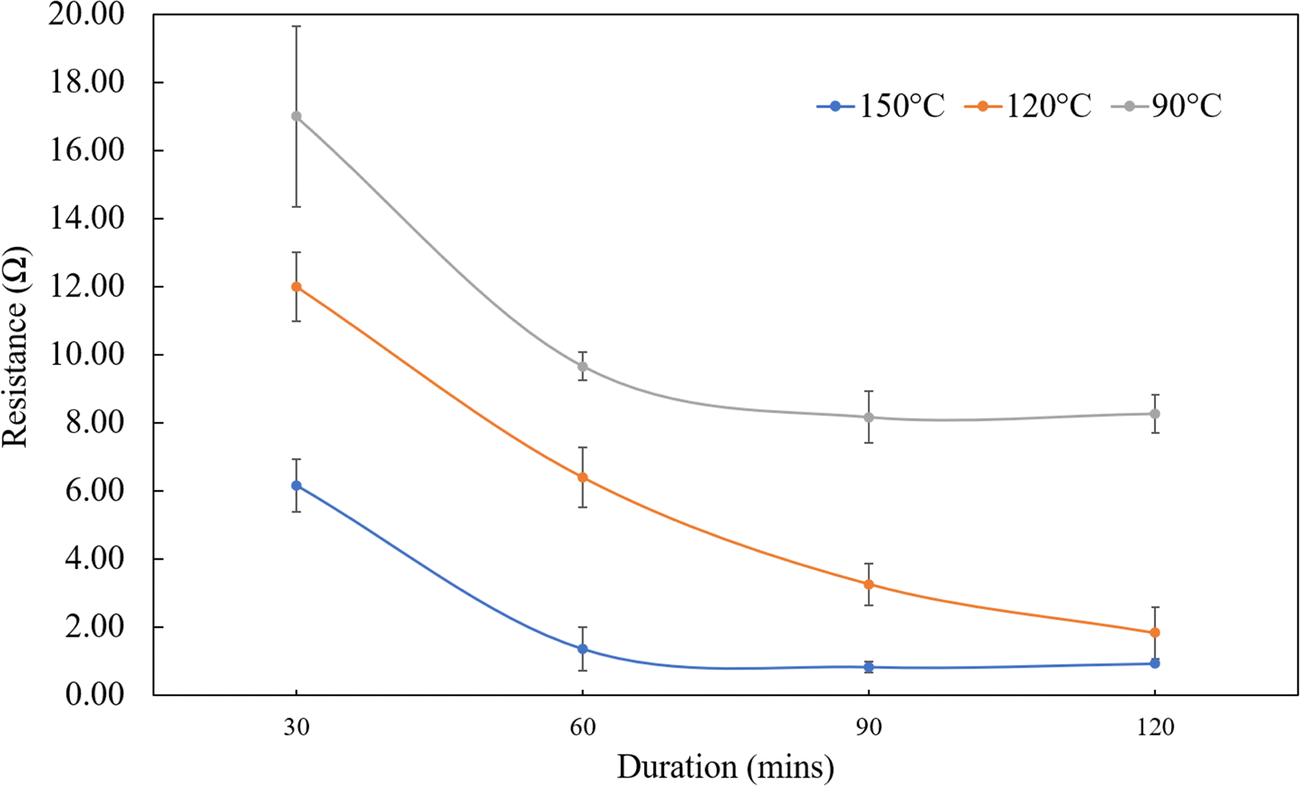
In this project, a DOD Dimatix Materials Printer DMP-2850 inkjet printer was used since they are commonly used for fabricating electronic devices.61–63Printing parameters like substrate temperature, drop spacing, and nozzle temperature are critical factors affecting the conductivity of printed patterns. The width of the printed pattern decreases with an increase in drop spacing, successively increasing the electrical resistance.64 The width of the pattern and electrical resistance decrease with an increase in substrate temperature, due to the coffee ring effect caused by the Marangoni flow in which the nanoparticles are collected on the edges forming thick layers. The lines printed at higher temperatures show greater thickness at the edges and consequently, the increase in the cross-sectional area results in lower resistance.65 An increase in nozzle temperature increases the line thickness and the cross-sectional area, resulting in a decrease in the electrical resistance.64 Further, the number of layers to be printed also contributes to the resistance values. Although adding a number of layers decreases the resistance value, it decreases the maximum breakdown strain a circuit can sustain irrespective of the shape of the pattern. Hence it is recommended that the optimum number of layers to be printed should be determined.66 In this work, based on the results mentioned by Abu-Khalaf et al.,66 we considered printing three layers. In addition to the inkjet printer parameters, the post-processing treatment such as sintering, which involves the merging of the particles, plays an important role in determining the conductivity of the printed electronic circuit of the wearable device. The resulting conductivity of the printed circuit highly depends on the temperature and duration of the post-processing. Particularly for silver NP ink, the temperature and duration of sintering are limited by the glass transition point, (Tg) of the polymeric substrate. Fig. 1 shows the effect of sintering time and temperature on the resistance of the silver pattern printed on the FKM. Electrical resistance decreases significantly with the increase in temperature and duration. From this study we observed resistance as low as 1Ω at 150 °C for 90 minutes. From this study we finalized our sintering temperature for the printed patterns.
 | ||
| Fig. 1 Effect of sintering time and temperature on the resistance. | ||
For the overall print quality, it is essential to consider printing parameters like waveform, jetting voltage, and cartridge temperature since these parameters influence the drop formation and drop diameter. The volume of the drop can be controlled by waveform parameters, velocity can be controlled by the jetting voltage and cartridge temperature, and the geometry of the drop can be controlled by the jetting voltage and waveform parameters.67 Thus, after multiple trials, we finalized the parameters suitable for our printing, as shown in Table 3.
| Inkjet printing parameters | |
|---|---|
| Drop spacing (μm) | 15 |
| Substrate temperature (°C) | 45 |
| Nozzle temperature (°C) | 28 |
| Sintering temperature (°C) | 150 |
| Sintering time (h) | 1.5 |
| Jetting voltage (v) | 30.5 |
| Jetting frequency (kHz) | 5 |
| Number of layers | 3 |
Two patterns, called pattern A and pattern B were designed in the computer with certain dimensions. The designs and dimensions of the patterns for printing on the flexible substrate are shown in Fig. 2. This pattern was printed with silver ink on the FKM sheet. Details of the fabrication process are described in S1 ESI.†
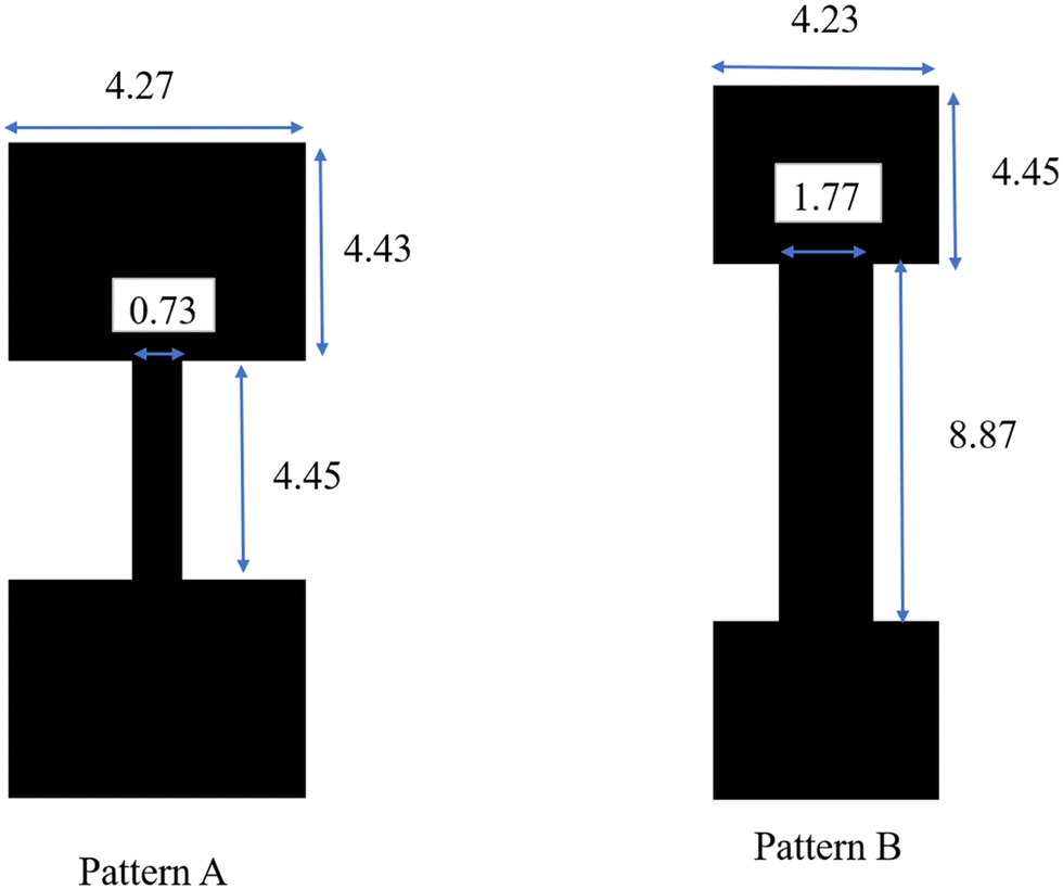 | ||
| Fig. 2 Design of the printed pattern with dimensions: (a) pattern A and (b) pattern B. Units: millimeters (mm). | ||
2.4 Encapsulation
Encapsulation of the printed pattern is essential for protection in harsh environmental conditions. In our study, FKM was used as the encapsulant material for sealing the printed pattern since it has excellent chemical and oil resistance.68 In this work, Viton™ fluoroelastomer (Fluorodyn™ Caulk, Thermodyn Corporation, USA)69 used as the sealant was applied on the periphery of the printed pattern. Further, the FKM sheet mentioned in section 2.1 has a similar thickness to that of the bottom FKM sheet and was placed on top of the printed pattern such that the entire assembly was encapsulated. Fig. 3. shows our encapsulation process. Before the start of the encapsulation process, the connecting wires are glued on the printed pattern using silver paste (8331D silver conductive epoxy adhesive, MG Chemicals, USA),70 then the FKM sealant is applied on the periphery of this printed pattern at ambient temperature. Next, the FKM sheet is placed over the top of the bottom sheet and pressed over the FKM caulk forming a permanent seal. Finally, the whole assembly is kept at room temperature for 48 hours to dry. Further, once the sealant is dried, it is recommended that curing is done in increments as sudden heating of the wet caulk will result in blistering of the caulk surface. Curing should be started at 37.7 °C with an increase of 10 °C every 30 minutes up to 120 °C, and once the solvent has evaporated, hold the temperature for 1 hour to fully cure the caulk.69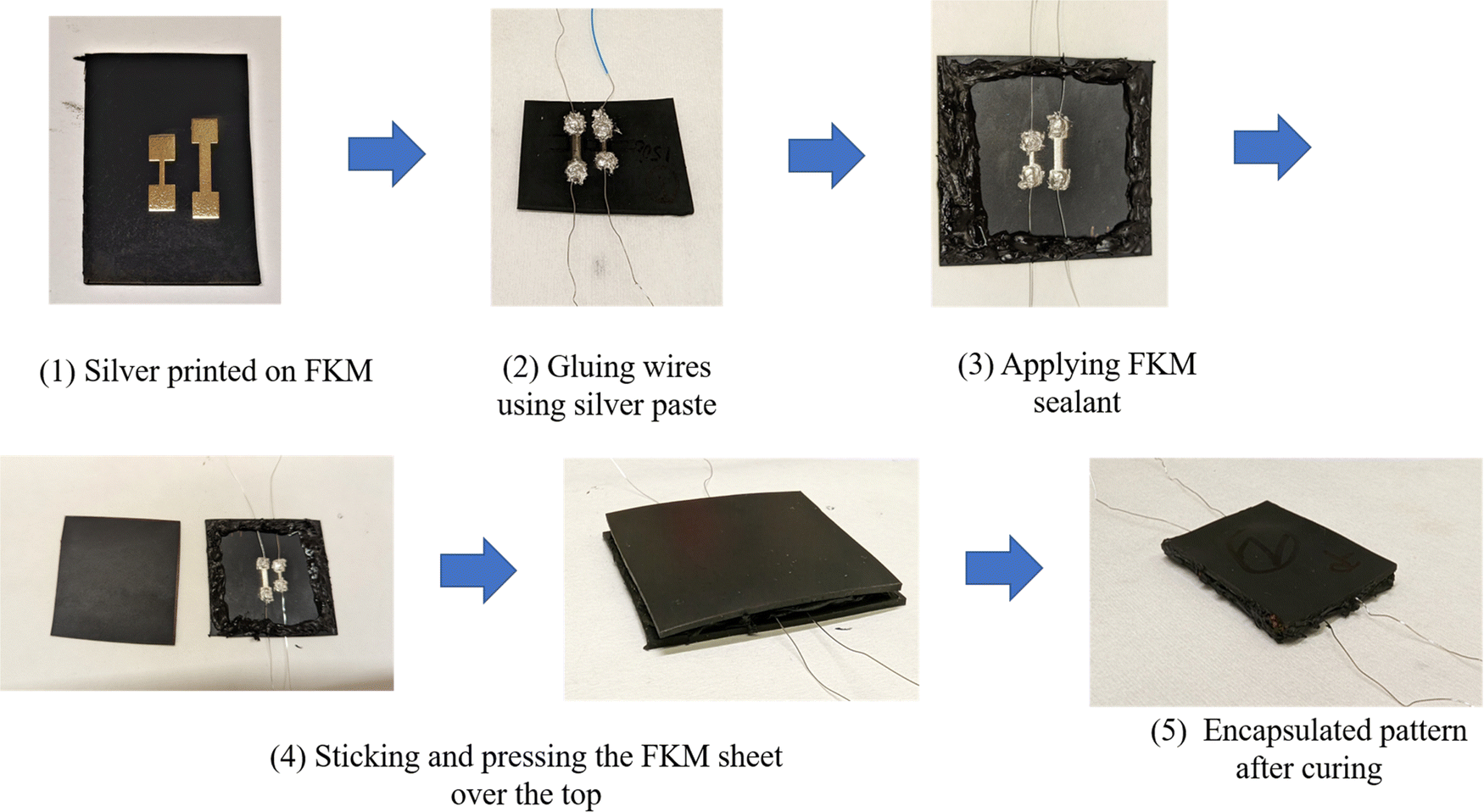 | ||
| Fig. 3 Encapsulation of a printed silver pattern on the substrate. | ||
The thickness of the encapsulation layer is critical since it might affect the stress produced on the conductive pattern. The thickness of the encapsulation layer was determined using the neutral axis principle, which states that a “neutral axis is an axis in the cross-section wherein longitudinal stress or strain is zero”. Considering the geometry as a composite beam in bending we could calculate the neutral axis/neutral plane of a composite beam by using the equation.71
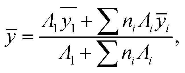 | (1) |
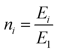 , A = cross-sectional area, E = Young's modulus,
 ![[y with combining overline]](https://www.rsc.org/images/entities/i_char_0079_0305.gif) = neutral axis distance from the datum,
= neutral axis distance from the datum, 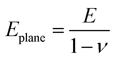 is used for neutral plane calculation, ν = Poisson ratio.
Fig. 4 shows generic neutral axis parameters used for calculation of the thickness. Neutral axis calculations are explained in S2 ESI.†
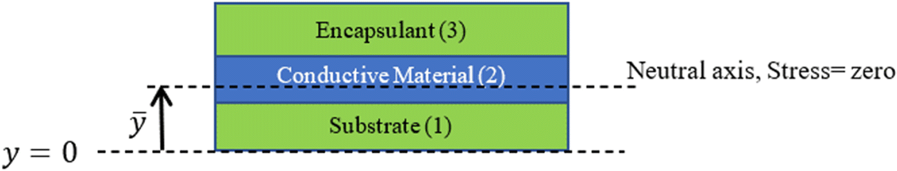 | ||
| Fig. 4 Generic neutral axis parameters are used for calculation of the thickness. | ||
In our case, the thickness of the encapsulant layer to be applied to the printed geometry was determined by using eqn (1). We engineered the thickness of the encapsulant material in such a way that the neutral axis passed through the conductive material, thus it will not have longitudinal stress or strain72 helping to minimize the cracks and improve the conductivity and overall quality of the printed electronics. Cross-sectional structures using a fluoroelastomer as an encapsulant are illustrated in S3 ESI.†
2.5 Characterization
We measured the resistance values using a digital multimeter. Dimensions of the printed pattern, i.e., length and width, were measured by a vision measuring system (Quick Vision Active, Mitutoyo QV-L202Z1L-D) and the thickness of the printed pattern was measured using a 3D optical profilometer (Zygo, Nexview™). Conductive extension wires were glued to the circuits to evaluate the electrical performance after curing the encapsulant. The entire assembly with the encapsulant material was kept for curing at room temperature for 24 h. The cured encapsulated samples were submerged under commercial hydraulic oil (MAG 1 AW ISO 46 hydraulic oil). We selected this oil since it had a flashpoint of 225 °C which was essential for our experiments to evaluate the resistance values for temperatures up to 180 °C. As shown in Fig. 5, the setup for testing the samples comprises a digital multimeter to measure the resistance, an encapsulated sample dipped in hydraulic oil, a hot plate as a heat source, and a temperature monitoring probe.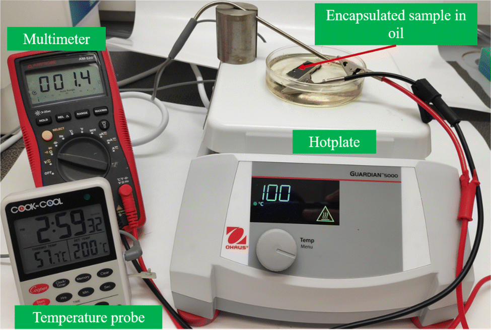 | ||
| Fig. 5 Setup for testing the encapsulated samples at elevated temperatures. | ||
A mass variation test was performed on FKM, PDMS, and PET using a weighing scale (Mettler Toledo, XS1203S). The FTIR spectra of FKM before and after treatment with oil were captured using a PerkinElmer Frontier MIR/FIR spectrometer and microscopic images before and after treatment with oil were taken using an Olympus MX61 microscope. Contact angle was measured by ramé-hart Model 210 Goniometer/Tensiometer.
3. Results and discussions
3.1 Performance evaluation of the printed pattern
Contact angles were measured before and after the surface treatment, as shown in Table 4. For good printing and adhesion, the surface tension of the ink needs to be lower than the surface energy of the substrate.73 Since all the contact angles measured are <90° after surface treatment, it implies that the ink can spread uniformly and wet the substrate, which was desired.| Contact angle in degrees | ||
|---|---|---|
| Substrate | Before surface treatment | After surface treatment |
| FKM | 101.2 | 56.66 |
The width and length of the printed pattern were compared with the intended design of our pattern. The printed dimensions were found to be comparable with the dimensions we designed. Fig. 6 shows the printed patterns on fluoroelastomer rubber. From the results, a uniform printed pattern can be evidently seen, with fewer cracks since we achieved a surface energy match between the ink and the substrate.
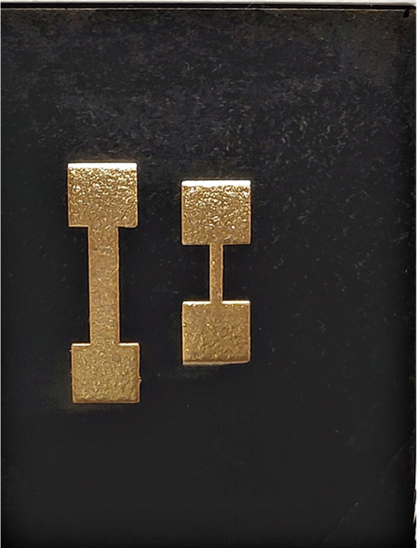 | ||
| Fig. 6 Printed results on fluoroelastomer rubber. | ||
We fabricated each pattern 5 times on the substrate. We measured the thickness of the layers using a 3D profilometer as shown in Fig. 7. For each pattern, we measured the thickness in at least three locations of the top pad, trace, and bottom pad, and calculated the average thickness.
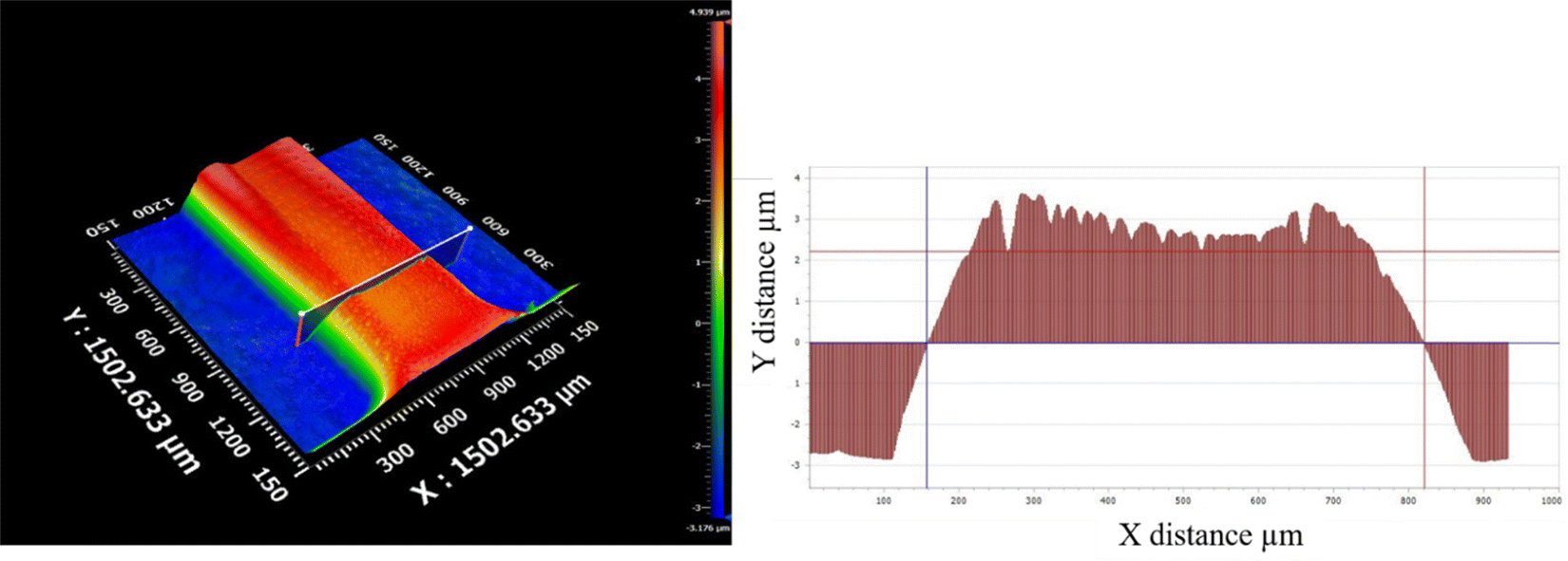 | ||
| Fig. 7 Thickness measurement of a printed pattern using a Zygo 3D profilometer. | ||
After measuring the dimensions, we calculated the theoretical resistance values using the following equation,
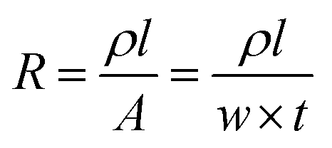 | (2) |
We measured the actual resistance values of the printed patterns using the digital multimeter. Table 5 shows the average thickness, and the theoretical and actual resistance values on each substrate. Though the resistance values i.e., the actual (measured) and theoretical (calculated), were not the same, but they were comparable. Table 5 shows that the actual resistance values are higher than the theoretical resistance values. The cause of this can be due to microscopic cracks in the printed pattern. These cracks can be reduced and conductivity can be improved by optimizing the parameters i.e., decreasing the drop spacing and increasing the sintering temperature and duration.64 However, reducing the drop spacing will shrink the size of the geometry and increasing the sintering temperature and the duration may damage the substrate. Sintering duration and temperature play an important role in improving the conductivity of the printed pattern as illustrated in Fig. 1. Further, conductivity can be improved by using silver nanoparticles (AgNPs) of various size distributions.74 Large-size AgNPs form a conductive path as they start to melt and contact each other with the rise in sintering time or temperature, whereas small AgNPs pack into the gaps created between the larger-size AgNPs. Thus, AgNPs sinter together to form a 3D conductive network due to high sintering temperatures or longer sintering times.75 However, using different sizes of silver particles might block the inkjet printer nozzle, which will impact the printing process.
| Average thickness (μm) | Theoretical resistance (Ω) | Actual resistance (Ω) | |
|---|---|---|---|
| Pattern A | 1.209 | 0.75 | 1.42 |
| Pattern B | 1.143 | 0.40 | 1.1 |
3.2 Performance evaluation in a harsh environment
| Resistance (Ω) | ||
|---|---|---|
| Pattern A | Pattern B | |
| Average | 1.8 | 1.6 |
| Maximum | 2.5 | 2.4 |
| Minimum | 1.4 | 1.1 |
| Std deviation | 0.30 | 0.38 |
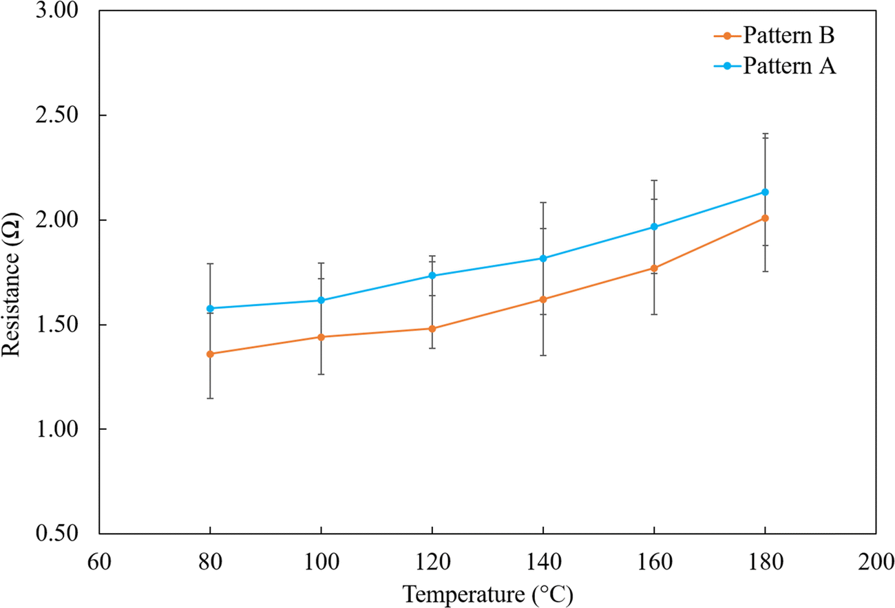 | ||
| Fig. 8 Trend in resistance values at elevated temperatures. | ||
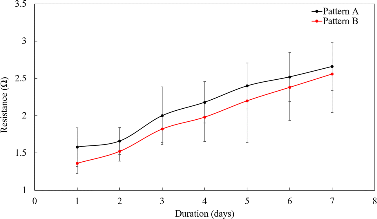
The average resistance values slightly increased at elevated temperatures compared to the average resistance values at room temperature. This increase might be due to the inherent property of metals to increase in resistance with a temperature rise.76 However the standard deviation value was <1, which proves the effectiveness of the FKM as an encapsulant material in harsh environmental conditions. Hence, the second objective was achieved i.e., examining the potential of FKM as an encapsulation material for the printed flexible electronics patterns in hydrocarbon liquids at elevated temperatures. Further to evaluate the effectiveness of FKM as an encapsulant, we tested pristine (non-encapsulated) and encapsulated samples at the highest temperature of our experiment i.e., at 180 °C for 24 hour cycles. We noted the initial resistance of the sample (Ainitial = 1.42 Ω and Binitial = 1.1 Ω) before the start of the test and after completing each cycle we recorded the resistance at room temperature by using a digital multimeter. After completing the first cycle of 24 hours, all non-encapsulated samples were non-functional, and were eliminated from the test, whereas the encapsulated samples were functioning. Further, this test was continued for the encapsulated electronics for 7 cycles of 24 hours each i.e., a total duration of 1 week. Fig. 9 shows the trend of change in resistance for one week.
 | ||
| Fig. 9 Trend of change in resistance for one week. | ||
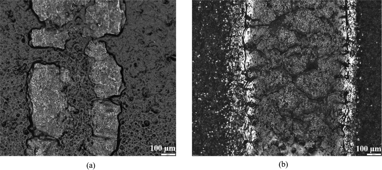
From Fig. 9 it is evident that the encapsulated samples continued to show an increase in resistance values until the seventh day (1 week). After a week, we tear down the sample to analyze it under microscope. Fig. 10 shows the silver pattern on the non-encapsulated (a) and encapsulated samples (b).
 | ||
| Fig. 10 Silver pattern on the non-encapsulated (a) and encapsulated samples (b). | ||
From Fig. 10 it is evident that the silver printed on the encapsulated samples has minor cracks; however, they were in a better condition than the non-encapsulated samples. Furthermore, after the test, the thickness of the silver pattern in the encapsulated samples was found to be significantly better compared to the non-encapsulated samples and was comparable to the pristine printed pattern mentioned in Table 5. The thickness of the printed pattern in the encapsulated samples is mentioned in S4 ESI.† This implies that FKM was successfully able to shield the printed silver patterns in the stated harsh environmental conditions. Further, considering this trend of an increase in resistance over 7 days and assuming a final breakdown resistance of 1 MΩ, we can estimate the ideal time for the circuit to be nonfunctional. However, several supplementary factors need to be addressed like corrosion of the connecting wires, degradation of the joint between the connecting wire and the pad of the printed pattern, oil seeping through the connecting wires, the sealant joint between the two FKM sheets, etc. These factors need to be addressed by continuous improvement of the design for the circuits so that they last longer.
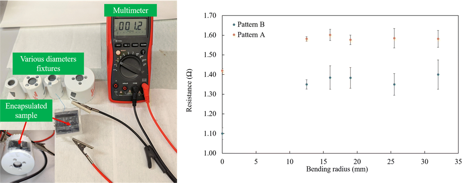 | ||
| Fig. 11 Bending test of the encapsulated pattern at various bending radii. | ||
3.3 Silver, FKM, and hydrocarbon fluid interaction
Since this is the first attempt to fabricate silver patterns directly on FKM for application in a hydrocarbon fluid environment, it is essential to study the interaction between the silver, FKM, and hydrocarbon fluid. In this study, silver is a conductive material and is crucial to the flexible printed pattern that is subjected to high-temperature hydrocarbon fluids. Thus, the protection of the silver from such harsh conditions is of prime importance. Silver has a high tendency to react with moisture, O2, and extremely low levels of hydrogen sulfide (H2S) in the atmosphere, creating corrosion, oxidation, and sulfidation respectively.78,79FKM has excellent resistance to oil, fuel, water, O2, and heat due to the strong structural chemistry i.e., the C–F bond energy = 485 kJ mol−1.80,81 In this study, silver electrodes are printed on the FKM sheet, thus it is important to consider the Ag-FKM compatibility. Based upon the FKM compatibility chart published by Chemours, it is evident that silver compounds are non-reactive with FKM.80 Furthermore, researchers have successfully formulated silver-FKM inks for fabricating stretchable conductors without reporting any degradation in the internal stucture.30–33 This illustrates that FKM and silver are compatible. Since FKM has good resistance to oil, fuel, water, O2, and heat it can shield the silver electrodes from corrosion and oxidation. However, the presence of sulfur in the air is the primary reason for silver corrosion. Sulfur is present in the air in the form of carbonyl sulfide (OCS) and can react with water vapor in the atmosphere to produce H2S,
| OCS + H2O(g) → H2S + CO2 | (3) |
| 2Ag + H2S → Ag2S + H2 | (4) |
These silver sulfide (Ag2S) particles will reduce the conductivity and degrade the performance.79 However, in our study we submerge the flexible patterns in a hydrocarbon fluid which will cut off atmospheric air and moisture. Further, modern oil production technologies limit the amount of elemental sulfur and hydrogen sulfide that may cause corrosion to metals.82 The United States Environmental Protection Agency (EPA) requires that the sulfur content of gasoline should be less than 10 ppm.83 Furthermore compared to natural rubber which is vulcanized by sulfur, FKM is vulcanized by using peroxide and bisphenol AF which are non-sulfur agents,84,85 thus minimizing the overall sulfur content coming in contact with the printed silver pattern. Additionally, the coatings mentioned by Guan et al. can be used on the silver to prevent corrosion.79
According to the chemical compatibility chart published by Chemours.80 FKM also does not have excellent compatibility with H2S. However, some researchers have proven the effectiveness of FKM in certain concentration limits of H2S by developing and testing sensor packaging for a downhole monitoring microsystem,23 and an O ring made from Viton extreme for pipelines valves.86 In addition to H2S, FKM is not compatible with acetone, esters, amines, organic acids, acetic acid, methyl ethyl ketone (MEK), ethyl acetate, or highly polar chemicals.87 Degradation mechanisms of the FKM encapsulant need to be considered since it will be continuously subjected to hydrocarbon fluids under high-temperature conditions. Normally, the polymer is degraded by two processes: chemical aging (chain scission, crosslinking) and physical aging (chain relaxation, swelling). Many researchers have reported the degradation of FKM in several ways.88Table 7 lists the degradation mechanisms of FKM.
| Ref. | Medium of exposure | FKM degradation mechanism |
|---|---|---|
| Donghan et al. 201889 | Alkaline | Fluorine and hydrogen atoms on the FKM backbone react to form hydrofluoric acid (HF) and generate a C![[double bond, length as m-dash]](https://www.rsc.org/images/entities/char_e001.gif) C bond. C bond. |
| The formation of CC bonds is more susceptible to harsh conditions resulting in polymer degradation. |
||
| Mitra et al. 200390,91 | Alkaline | The reaction between HF and alkaline accelerates the degradation. |
| Akhlaghi et al. 201792 | Biodiesel | CC bond in FKM reacts with an unsaturated component of biodiesel promoting chain scission. |
| Akhlaghi et al. 2016,93 Sugama 2001,94 Lin et al. 2011,95 Sugama et al. 201596 | Geothermal (water/oxygen) | The presence of oxygen disturbs the C–F bond, through a three-stage oxidation mechanism, impacting the thermal stability of FKM. |
| Song et al. 202297 | Gamma radiation and heat | Decrease in C–H bonds and formation of the functional group containing oxygen and double bonds such as C–O, CO, and CC by auto-oxidation. |
| The auto-oxidation process forms cross links with oxygen and reduces mobility, causing fluoroelastomer hardening. |
Apart from this mechanism, the degradation of FKM is dependent upon the properties of the medium such as the solubility parameter, chemical structure, and interaction between the medium and polymer molecule.88
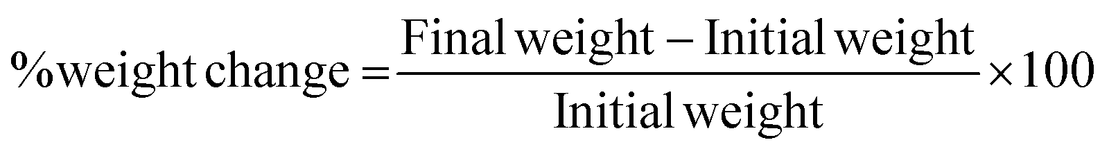
In this study, we have subjected FKM to the coupled effects of high temperatures and a hydrocarbon fluid. We evaluate the degradation by using (1) mass variation, (2) microscopic images and (3) FTIR spectroscopy.
 | (5) |
| Substrate | Duration (weeks) | % weight change |
|---|---|---|
| PDMS | 2 | 5.45 |
| PET | 2 | 16.7 |
| FKM | 20 | 2.66 |
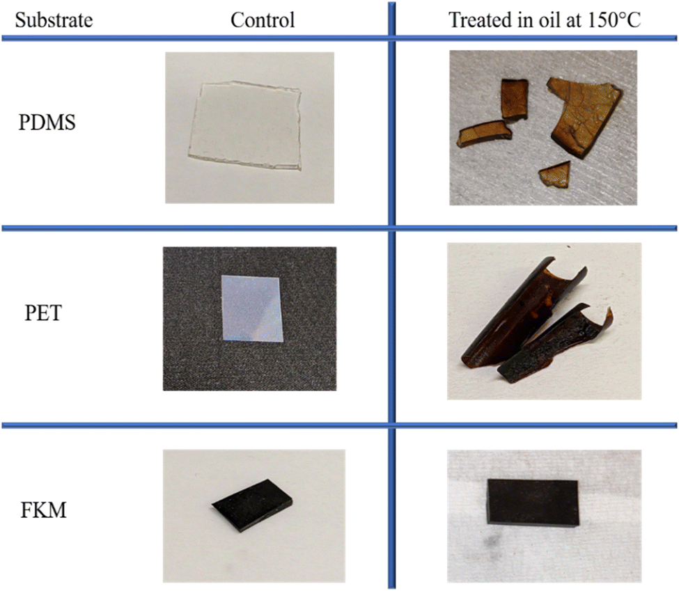 | ||
| Fig. 12 Physical appearance of PDMS, PET, and FKM before and after the test. | ||
A considerable gain in weight was observed for the PDMS and PET samples; however, a negligible gain in weight was observed in FKM for the stated duration. PDMS physically broke down in oil since it is not compatible with most hydrocarbons and oils.100 PET broke down and it was obvious that the operating temperature range of PET was not compatible with this study. FKM neither showed a change in physical appearance nor a considerable change in weight due to the high electronegative fluorine atoms in the fluoroelastomer which helped it to resist the degradation caused by the hydrocarbon fluids at high temperatures. Thus, FKM showed much better resistance to degradation compared to PDMS and PET for the stated harsh environmental conditions.
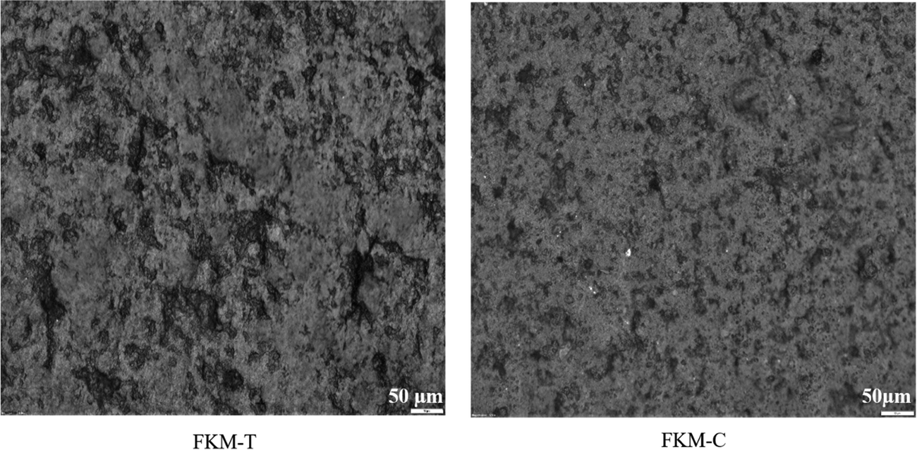 | ||
| Fig. 13 Microscopic images of the FKM-T and FKM-C. | ||
| Position | FKM-T | FKM-C |
|---|---|---|
| 1 | 1.043 | 0.803 |
| 2 | 1.133 | 0.867 |
| 3 | 0.962 | 1.106 |
| 4 | 0.878 | 0.908 |
| 5 | 0.954 | 0.938 |
| Average | 0.994 | 0.924 |
The surface roughness Ra (μm) of FKM-C and FKM-T shows that the treated sample has marginally higher roughness as compared to the control sample. Thus, from the microscopic images and roughness values, we can infer a marginal degradation found on FKM after treatment in oil at 150 °C for 20 weeks. Furthermore, we did not find any voids, cracks, or particle agglomeration in the treated sample. This implies that FKM was able to withstand the harsh hydrocarbon fluid conditions.
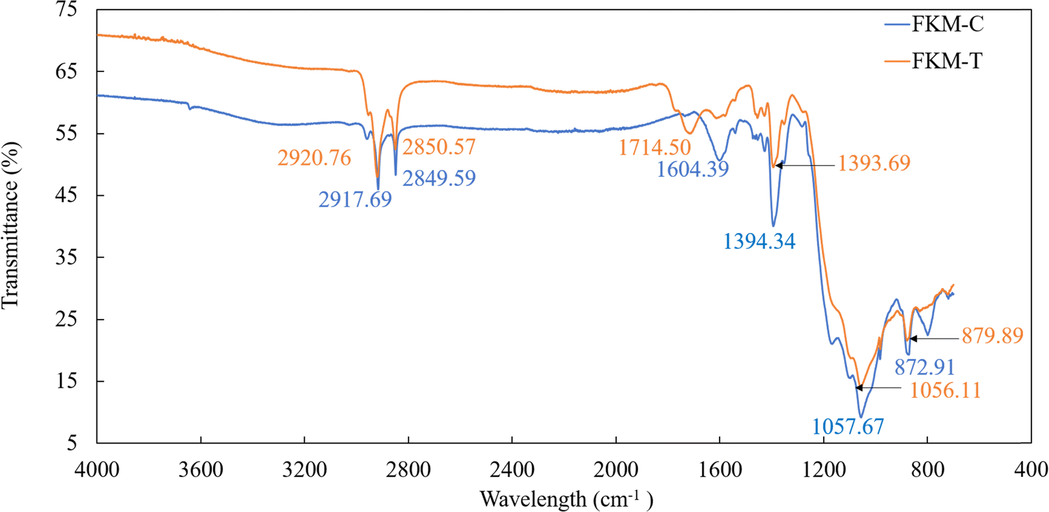
C stretching peaks show a slight shift from 1604.39 cm−1 to 1714.50 cm−1. The peak has shifted towards a higher wavenumber which implies that the mass of the molecule is reduced, which can be attributed to Hooke's law in IR spectroscopy.101 It states that the frequency of vibration is inversely proportional to the mass of the vibrating molecules, hence the lighter the molecule the greater the frequency of vibration and the higher the wave number. This loss in the molecular mass may be attributed to the beginning of the degradation; however, peaks are still visible in FKM-T after 20 weeks which shows its strong resistance to degradation. Thus, comparing the FTIR spectra of FKM-T and FKM-C we can infer there is no disappearance of the characteristics peaks of FKM, no new peak formation due to interactions with the oil during treatment, the strongest peak maintains its presence even after 20 weeks, and there is a negligible decrease in CH intensity which means that there are no dehydrofluorination reactions. Hence, it implies that FKM was able to withstand the harsh hydrocarbon fluid conditions without significant degradation.
 | ||
| Fig. 14 FTIR spectra of FKM-T and FKM-C. | ||
All three characterization techniques prove that the FKM used in this study was able to withstand the given harsh conditions with negligible degradation. Further, in our previous study,102 we proved the effectiveness of FKM as an encapsulant by encapsulating PET, PDMS, and silicone rubber and testing the samples in a harsh hydrocarbon fluid environment.
Furthermore, there are some alternatives to FKM for use at high temperatures and that demonstrate chemical resistance i.e. perfluoro elastomers (FFKM) are specifically used for high-temperature applications >200 °C,23 and AFLAS® (the trade name of the fluoroelastomer based upon an alternating copolymer of tetrafluoroethylene and propylene (TFE/P)) can resist temperatures up to 230 °C.103 However, these elastomers are extremely expensive compared to FKM, thus considering the final applications, a balance between the cost of the material and its compatibility with the environment needs to be considered.
Comparing the results of our work with existing literature will be challenging since inkjet printing on any substrate relies on several parameters like surface energy matching between the ink and substrate, viscosity, number of layers printed, and dimensions of the printed patterns, etc. Most of the researchers use ink and substrates with a suitable viscosity and surface energy for their applications. However, some research articles can be related to our work. For simplicity, we compared the resistance values obtained in our work at room temperature and no mechanical load conditions, as illustrated in Table 10. PDMS is the most used substrate and silver ink is the conductive material printed using inkjet printing by most of the researchers, which is like our work, where we are depositing silver on a FKM substrate. Thus, from Table 10 we were able to achieve the lowest possible resistance at room temperature and no mechanical load conditions.
4. Conclusion
In this study, we printed silver patterns on flexible FKM substrates. After printing, we measured the thickness of the pattern, calculated the theoretical resistance, and measured the actual resistance of the pattern. Although the theoretical versus actual resistance values from our printed pattern were not the same but were comparable, it implies that we achieved a desirable print and successfully overcame the challenges of surface energy mismatch, ink-substrate interaction, non-uniform layer thickness, and cracks, thus proving the consistency of our process. For the first time, silver ink was successfully printed on a FKM sheet using inkjet printing technology. We encapsulated the circuits using a fluoroelastomer and evaluated the performance of the circuit in commercially available hydraulic oil (MAG 1 AW ISO 46 hydraulic oil) at elevated temperatures, which revealed a negligible change in resistance for temperatures up to 180 °C. A bending test was performed where a negligible change in performance was found. Finally, degradation of the silver and FKM was characterized using mass variation, microscopic images, and FTIR spectroscopy, which revealed negligible degradation of the flexible encapsulated patterns. Since we were able to print a conductive pattern directly on FKM, this opens many opportunities for developing sensor electrodes using a FKM substrate which has excellent temperature, chemical, and oil resistance properties. These printed conductive patterns can be further used as sensor electrodes in a variety of applications like automotive, oil, and gas industries in which electronics products are directly in contact with hydrocarbon fluids.Author contributions
X. D. and A. S. conceived the idea. X. D. supervised the research. S. W. and X. D. wrote the manuscript. S. W. prepared all the figures and tables. All authors reviewed the manuscript and provided corrections and comments.Nomenclature
| T g | Glass transition temperature |
| R | Electric resistance |
| ρ | Resistivity |
| A | Cross-sectional area |
| l | Length of the pattern |
| t | Thickness of the pattern |
| w | Width of the pattern |
| E | Young's modulus |
|
| Neutral axis |
| ν | Poisson ratio |
Conflicts of interest
The authors declare no conflict of interest. This work is supported by the Saudi Arabian Oil Company (Saudi Aramco), Saudi Arabia. Any opinions, findings, conclusions, or recommendations expressed in this material are those of the authors and do not necessarily reflect the views of Saudi Aramco.Acknowledgements
We acknowledge funding and technical support from the Saudi Arabian Oil Company (Saudi Aramco).References
- Experimental Evaluation and Comparison of Thermal Conductivity of High-Voltage Insulation Materials for Vacuum Electronic Devices, https://www.springerprofessional.de/en/experimental-evaluation-and-comparison-of-thermal-conductivity-o/12144570, (accessed 15 March 2022).
- A. S. Almuslem, S. F. Shaikh and M. M. Hussain, Flexible and Stretchable Electronics for Harsh-Environmental Applications, Adv. Mater. Technol., 2019, 4, 1900145 CrossRef.
- MEMS: Design and Fabrication, ed. M. Gad-el-Hak, CRC Press, Boca Raton, 2005 Search PubMed.
- C. Slater, R. Cojbasic, T. Maeder, Y. Leblebici and P. Ryser, Packaging technologies for high temperature control electronics, Addit. Conf. Device Packag. HiTEC HiTEN CICMT, 2013, 2013, 000184 CrossRef.
- A. Sajedi-Moghaddam, E. Rahmanian and N. Naseri, Inkjet-Printing Technology for Supercapacitor Application: Current State and Perspectives, ACS Appl. Mater. Interfaces, 2020, 12, 34487–34504 CrossRef CAS PubMed.
- R. Mikkonen, P. Puistola, I. Jönkkäri and M. Mäntysalo, Inkjet Printable Polydimethylsiloxane for All-Inkjet-Printed Multilayered Soft Electrical Applications, ACS Appl. Mater. Interfaces, 2020, 12, 11990–11997 CrossRef CAS PubMed.
- J. Wu, R. C. Roberts, N. C. Tien and D. Li, in IEEE SENSORS 2014 Proceedings, IEEE, Valencia, Spain, 2014, pp. 1100–1103.
- S. Jiang, Inkjet Printing of Nano-Silver Conductive Ink on PET Substrate, Mater. Eng, 2017 Search PubMed , https://digitalcommons.calpoly.edu/matesp/162/.
- M. A. Riheen, T. K. Saha and P. K. Sekhar, Inkjet Printing on PET Substrate, J. Electrochem. Soc., 2019, 166, B3036 CrossRef CAS.
- U. Löffelmann, J. G. Korvink, C. Hendriks, U. Schubert and P. Smith, Ink Jet Printed Silver Lines Formed in Microchannels Exhibit Lower Resistance Than Their Unstructured Counterparts, J. Imaging Sci. Technol., 2011, 55, 40302-1–40302–6 CrossRef.
- C.-Y. Chan, K.-C. Shih and T.-M. Huang, 2016 11th International Microsystems, Packaging, Assembly and Circuits Technology Conference (IMPACT), 2016, pp. 115–118 DOI:10.1109/IMPACT.2016.7800018.
- A. Boumeganane, A. Nadi, O. Cherkaoui and M. Tahiri, Inkjet printing of silver conductive ink on textiles for wearable electronic applications, Mater. Today: Proc., 2022, 58, 1235–1241 CAS.
- Y. Li, G. Wu, G. Song, S.-H. Lu, Z. Wang, H. Sun, Y. Zhang and X. Wang, Soft, Pressure-Tolerant, Flexible Electronic Sensors for Sensing under Harsh Environments, ACS Sens., 2022, 7, 2400–2409 CrossRef CAS PubMed.
- R. B. V. B. Simorangkir, Y. Yang, R. M. Hashmi, T. Bjorninen, K. P. Esselle and L. Ukkonen, Polydimethylsiloxane-Embedded Conductive Fabric: Characterization and Application for Realization of Robust Passive and Active Flexible Wearable Antennas, IEEE Access, 2018, 6, 48102–48112 Search PubMed.
- J. Trajkovikj, J.-F. Zurcher and A. K. Skrivervik, PDMS, A Robust Casing for Flexible W-BAN Antennas [EurAAP Corner], IEEE Antennas Propag. Mag., 2013, 55, 287–297 Search PubMed.
- E. J. R. Phua, M. Liu, B. Cho, Q. Liu, S. Amini, X. Hu and C. L. Gan, Novel high temperature polymeric encapsulation material for extreme environment electronics packaging, Mater. Des., 2018, 141, 202–209 CrossRef CAS.
- Handbook of Adhesive Technology, ed. A. Rudawska, CRC Press, 3rd edn, 2017 Search PubMed.
- N. Lakal, A. H. Shehri, K. W. Brashler, S. P. Wankhede, J. Morse and X. Du, Sensing technologies for condition monitoring of oil pump in harsh environment, Sens. Actuators, A, 2022, 346, 113864 CrossRef CAS.
- Standard Practice for Rubber and Rubber Latices—Nomenclature, https://www.astm.org/d1418-21a.html, (accessed 1 April 2022).
- Viton Rubber Seal | Compression Molding Services, https://qualiformrubbermolding.com/products/rubber-products/viton-rubber-seal/, (accessed 5 September 2022).
- Fluoroelastomers, FKM, FPM Info - Pelseal Technologies, https://www.pelseal.com/why-fluoroelastomers, (accessed 5 September 2022).
- G. Sharma, L. Klintberg and K. Hjort, Viton-based fluoroelastomer microfluidics, J. Micromech. Microeng., 2011, 21, 025016 CrossRef.
- N. Vellaluru, P. Dutta, A. Benken, G. Boero, R. Ordonez and Y. Gianchandani, Autonomous Sensing Microsystem with H2S Compatible Package and Enhanced Buoyancy for Downhole Monitoring, SPE J., 2022, 12 Search PubMed.
- M. M. Monshi, J.-S. Camara, S. Bhardwaj, J. L. Volakis and P. M. Raj, in 2020 IEEE 70th Electronic Components and Technology Conference (ECTC), IEEE, Orlando, FL, USA, 2020, pp. 835–840.
- J. Seo, J. Ha, B. Lee, H. Kim and Y. Hong, Fluoroelastomer encapsulation for enhanced reliability of solution-processed carbon nanotube thin-film transistors, Thin Solid Films, 2020, 704, 138021 CrossRef CAS.
- Y. Takahashi, T. Takahashi, T. Abe, H. Noma and M. Sohgawa, Tactile sensor with microcantilevers embedded in fluoroelastomer/PDMS for physical and chemical resistance, Electron. Commun. Jpn., 2022, 105, e12369 Search PubMed.
- J. Wang, B. Ye, C. An, B. Wu, H. Li and Y. Wei, Preparation and Properties of Surface-Coated HMX with Viton and Graphene Oxide, J. Energ. Mater., 2016, 34, 235–245 CrossRef CAS.
- S. Shajari, S. Ramakrishnan, K. Karan, L. J. Sudak and U. Sundararaj, Ultrasensitive wearable sensor with novel hybrid structures of silver nanowires and carbon nanotubes in fluoroelastomer: Multi-directional sensing for human health monitoring and stretchable electronics, Appl. Mater. Today, 2022, 26, 101295 CrossRef.
- H. Mu, W. Wang, L. Yang, J. Chen, X. Li, Y. Yuan, X. Tian and G. Wang, Fully integrated design of intrinsically stretchable electrodes for stretchable supercapacitors, Energy Storage Mater., 2021, 39, 130–138 CrossRef.
- A. Kumar, H. Saghlatoon, T.-G. La, M. Mahdi Honari, H. Charaya, H. Abu Damis, R. Mirzavand, P. Mousavi and H.-J. Chung, A highly deformable conducting traces for printed antennas and interconnects: silver/fluoropolymer composite amalgamated by triethanolamine, Flexible Printed Electron., 2017, 2, 045001 CrossRef.
- N. Matsuhisa, D. Inoue, P. Zalar, H. Jin, Y. Matsuba, A. Itoh, T. Yokota, D. Hashizume and T. Someya, Printable elastic conductors by in situ formation of silver nanoparticles from silver flakes, Nat. Mater., 2017, 16, 834–840 CrossRef CAS PubMed.
- N. Matsuhisa, M. Kaltenbrunner, T. Yokota, H. Jinno, K. Kuribara, T. Sekitani and T. Someya, Printable elastic conductors with a high conductivity for electronic textile applications, Nat. Commun., 2015, 6, 7461 CrossRef CAS PubMed.
- T. Zhong, N. Jin, W. Yuan, C. Zhou, W. Gu and Z. Cui, Printable Stretchable Silver Ink and Application to Printed RFID Tags for Wearable Electronics, Materials, 2019, 12, 3036 CrossRef CAS PubMed.
- O. A. Moses, L. Gao, H. Zhao, Z. Wang, M. Lawan Adam, Z. Sun, K. Liu, J. Wang, Y. Lu, Z. Yin and X. Yu, 2D materials inks toward smart flexible electronics, Mater. Today, 2021, 50, 116–148 CrossRef CAS.
- J. Sun, Y. Li, G. Liu, S. Chen, Y. Zhang, C. Chen, F. Chu and Y. Song, Fabricating High-Resolution Metal Pattern with Inkjet Printed Water-Soluble Sacrificial Layer, ACS Appl. Mater. Interfaces, 2020, 12, 22108–22114 CrossRef CAS PubMed.
- S. Khan, L. Lorenzelli and R. S. Dahiya, Technologies for Printing Sensors and Electronics Over Large Flexible Substrates: A Review, IEEE Sens. J., 2015, 15, 3164–3185 Search PubMed.
- D. Maddipatla, B. B. Narakathu and M. Atashbar, Recent Progress in Manufacturing Techniques of Printed and Flexible Sensors: A Review, Biosensors, 2020, 10, 199 CrossRef CAS PubMed.
- J. Sun, R. Sun, P. Jia, M. Ma and Y. Song, Fabricating flexible conductive structures by printing techniques and printable conductive materials, J. Mater. Chem. C, 2022, 10, 9441–9464 RSC.
- K. Yan, J. Li, L. Pan and Y. Shi, Inkjet printing for flexible and wearable electronics, APL Mater., 2020, 8, 120705 CrossRef CAS.
- A. Salim and S. Lim, Review of Recent Inkjet-Printed Capacitive Tactile Sensors, Sensors, 2017, 17, 2593 CrossRef PubMed.
- X. Du, S. P. Wankhede, S. Prasad, A. Shehri, J. Morse and N. Lakal, A review of inkjet printing technology for personalized-healthcare wearable devices, J. Mater. Chem. C, 2022, 10, 14091–14115 RSC.
- S. P. Sreenilayam, I. U. Ahad, V. Nicolosi, V. Acinas Garzon and D. Brabazon, Advanced materials of printed wearables for physiological parameter monitoring, Mater. Today, 2020, 32, 147–177 CrossRef.
- Q. Huang and Y. Zhu, Printing Conductive Nanomaterials for Flexible and Stretchable Electronics: A Review of Materials, Processes, and Applications, Adv. Mater. Technol., 2019, 4, 1800546 CrossRef.
- A. Sinha and Y. K. Joshi, Downhole Electronics Cooling Using a Thermoelectric Device and Heat Exchanger Arrangement, J. Electron. Packag., 2011, 133(4), 041005 CrossRef.
- Downhole Temperature – an overview | ScienceDirect Topics, https://www.sciencedirect.com/topics/engineering/downhole-temperature, (accessed 24 September 2022).
- A. Abdihamzehkolaei, M. T. Ahad and Z. Siddique, Volume Resistivity of Viton Polymer under Thermal Aging, Polymers, 2021, 13, 773 CrossRef CAS PubMed.
- Viton™ Product Selection Guide | VitonTM Fluoroelastomers, https://www.viton.com/en/products/product-selection, (accessed 3 December 2022).
- Viton™ Dipolymers A-Type | VitonTM A-Type Fluoroelastomers, https://www.viton.com/en/products/a-type, (accessed 3 December 2022).
- Std, 12 in × 12 in, Viton Sheet – 1MXU9|BULK-RS-V75-23 – Grainger, https://www.grainger.com/product/GRAINGER-APPROVED-Viton-Sheet-1MXU9, (accessed 3 December 2022).
- SYLGARD™ 184 Silicone Elastomer Kit, https://www.dow.com/en-us/pdp.sylgard-184-silicone-elastomer-kit.01064291z.html, (accessed 3 December 2022).
- Novele Printing Media, https://www.novacentrix.com/product/novele-printing-media/, (accessed 3 December 2022).
- B.-J. de Gans, P. C. Duineveld and U. S. Schubert, Inkjet Printing of Polymers: State of the Art and Future Developments, Adv. Mater., 2004, 16, 203–213 CrossRef CAS.
- H.-M. Ren, Y. Guo, S.-Y. Huang, K. Zhang, M. M. F. Yuen, X.-Z. Fu, S. Yu, R. Sun and C.-P. Wong, One-Step Preparation of Silver Hexagonal Microsheets as Electrically Conductive Adhesive Fillers for Printed Electronics, ACS Appl. Mater. Interfaces, 2015, 7, 13685–13692 CrossRef CAS PubMed.
- I. J. Fernandes, A. F. Aroche, A. Schuck, P. Lamberty, C. R. Peter, W. Hasenkamp and T. L. A. C. Rocha, Silver nanoparticle conductive inks: synthesis, characterization, and fabrication of inkjet-printed flexible electrodes, Sci. Rep., 2020, 10, 8878 CrossRef CAS PubMed.
- Silver Jet Ink | Nano-Silver Ink for Inkjet Printing | ANP Co., Ltd, https://anapro.com/eng/product/silver_inkjet_ink.html, (accessed 5 September 2022).
- ramé-hart instrument co. Monthly Newsletter, https://www.ramehart.com/newsletters/2021-03_news.htm, (accessed 23 August 2021).
- H. Zhang and N. Y. Lee, Non-silicon substrate bonding mediated by poly(dimethylsiloxane) interfacial coating, Appl. Surf. Sci., 2015, 327, 233–240 CrossRef CAS.
- M. A. Eddings, M. A. Johnson and B. K. Gale, Determining the optimal PDMS–PDMS bonding technique for microfluidic devices, J. Micromech. Microeng., 2008, 18, 067001 CrossRef.
- K. Haubert, T. Drier and D. Beebe, PDMS bonding by means of a portable, low-cost corona system, Lab Chip, 2006, 6, 1548–1549 RSC.
- A. Borók, K. Laboda and A. Bonyár, PDMS Bonding Technologies for Microfluidic Applications: A Review, Biosensors, 2021, 11, 292 CrossRef PubMed.
- Y.-Z. Zhang, Y. Wang, T. Cheng, W.-Y. Lai, H. Pang and W. Huang, Flexible supercapacitors based on paper substrates: a new paradigm for low-cost energy storage, Chem. Soc. Rev., 2015, 44, 5181–5199 RSC.
- H. Sirringhaus, T. Kawase, R. H. Friend, T. Shimoda, M. Inbasekaran, W. Wu and E. P. Woo, High-Resolution Inkjet Printing of All-Polymer Transistor Circuits, Science, 2000, 290, 2123–2126 CrossRef CAS PubMed.
- Y.-Z. Zhang, Y. Wang, T. Cheng, L.-Q. Yao, X. Li, W.-Y. Lai and W. Huang, Printed supercapacitors: materials, printing and applications, Chem. Soc. Rev., 2019, 48, 3229–3264 RSC.
- Y. Kim, X. Ren, J. W. Kim and H. Noh, Direct inkjet printing of micro-scale silver electrodes on polydimethylsiloxane (PDMS) microchip, J. Micromech. Microeng., 2014, 24, 115010 CrossRef.
- B. Derby, Inkjet Printing of Functional and Structural Materials: Fluid Property Requirements, Feature Stability, and Resolution, Annu. Rev. Mater. Res., 2010, 40, 395–414 CrossRef CAS.
- J. Abu-Khalaf, L. Al-Ghussain, A. Nadi and A. Al-Halhouli, Conductivity and Stretchability of Inkjet-Printed Silver Nanoparticle Patterns: Effect of the Number of Printed Layers, Int. J. Mech. Eng. Robot. Res., 2020, 528–534 CrossRef.
- N. Mohan, S. K. Bhogaraju, M. Lysien, L. Schneider, F. Granek, K. Lux and G. Elger, in 2021 23rd European Microelectronics and Packaging Conference & Exhibition (EMPC), IEEE, Gothenburg, Sweden, 2021, pp. 1–6.
- P. T. LLC, Fluoroelastomers, FKM, FPM Info - Pelseal Technologies, https://www.pelseal.com/why-fluoroelastomers, (accessed 27 March 2022).
- Fluorodyn™ Caulk (made with VitonTM), https://www.thermodynglobal.com/product/viton-caulk/, (accessed 5 September 2022).
- 8331D - Silver Conductive Epoxy Adhesive, https://www.mgchemicals.com/products/adhesives/electrically-conductive-adhesives/silver-epoxy/, (accessed 30 December 2022).
- A. C. Ugural and S. K. Fenster, Part of the International Series in the Physical and Chemical Engineering Sciences series, Advanced Mechanics of Materials and Applied Elasticity, 6th Edition, Pearson, 6th edn, 2019 Search PubMed.
- D.-H. Kim, N. Lu, R. Ma, Y.-S. Kim, R.-H. Kim, S. Wang, J. Wu, S. M. Won, H. Tao, A. Islam, K. J. Yu, T. Kim, R. Chowdhury, M. Ying, L. Xu, M. Li, H.-J. Chung, H. Keum, M. McCormick, P. Liu, Y.-W. Zhang, F. G. Omenetto, Y. Huang, T. Coleman and J. A. Rogers, Epidermal Electronics, Science, 2011, 333, 838–843 CrossRef CAS PubMed.
- N. Ibrahim, J. O. Akindoyo and M. Mariatti, Recent development in silver-based ink for flexible electronics, J. Sci.: Adv. Mater. Devices, 2022, 7, 100395 CAS.
- J. Ding, J. Liu, Q. Tian, Z. Wu, W. Yao, Z. Dai, L. Liu and W. Wu, Preparing of Highly Conductive Patterns on Flexible Substrates by Screen Printing of Silver Nanoparticles with Different Size Distribution, Nanoscale Res. Lett., 2016, 11, 412 CrossRef PubMed.
- M. Matsubara, T. Yonezawa, T. Minoshima, H. Tsukamoto, Y. Yong, Y. Ishida, M. T. Nguyen, H. Tanaka, K. Okamoto and T. Osaka, Proton-assisted Low-temperature Sintering of Cu Fine Particles Stabilized by a Proton-initiating Degradable Polymer, RSC Adv., 2015, 5, 102904 RSC.
- Temperature effects on resistance, https://learnabout-electronics.org/Resistors/resistors_01a.php, (accessed 5 September 2022).
- J. Yang, D. Zi, X. Zhu, H. Li, Z. Li, L. Sun, G. Zhang, F. Wang, Z. Peng and H. Lan, Printed Flexible Transparent Electrodes for Harsh Environments, Adv. Mater. Technol., 2022, 7, 2101087 CrossRef CAS.
- T. E. Graedel, Corrosion Mechanisms for Silver Exposed to the Atmosphere - IOPscience, J. Electrochem. Soc., 1992, 139, 1963 CrossRef CAS.
- P. Guan, R. Zhu, Y. Zhu, F. Chen, T. Wan, Z. Xu, R. Joshi, Z. Han, L. Hu, T. Wu, Y. Lu and D. Chu, Performance degradation and mitigation strategies of silver nanowire networks: a review, Crit. Rev. Solid State Mater. Sci., 2022, 47, 435–459 CrossRef CAS.
- CRG: Chemical Resistance of VitonTM - Selection Guide, https://chemours-util.my.salesforce-sites.com/CRG_VitonGuide, (accessed 17 December 2022).
- Chemical degradation of an uncrosslinked pure fluororubber in an alkaline environment - Mitra - 2004 - Journal of Polymer Science Part A: Polymer Chemistry - Wiley Online Library, https://onlinelibrary.wiley.com/doi/10.1002/pola.20473, (accessed 17 December 2022).
- Removal of Hydrogen Sulfide from Diesel Fuels, https://fuelcleaning.globecore.com/removal-hydrogen-sulfide-diesel-fuels-current-technologies/, (accessed 17 December 2022).
- Gasoline Sulfur, https://www.epa.gov/gasoline-standards/gasoline-sulfur, (accessed 17 December 2022).
- VitonTM Product Selection Guide | VitonTM Fluoroelastomers, https://www.viton.com/en/products/product-selection, (accessed 17 December 2022).
- United States, US7060739B2, 2006.
- J. Heidarian and H. H. Khanli, Verification Properties of O-rings made from Viton Extreme with Advanced Polymer Architecture used in Pipeline Valves Containing very Sour Gas, J. Appl. Sci., 2010, 10, 2693–2696 CrossRef CAS.
- Viton Chemical Compatibility Chart, https://www.calpaclab.com/viton-chemical-compatibility-chart/, (accessed 17 December 2022).
- Q.-L. Wang, J.-K. Pei, G. Li, X. He, Y.-H. Niu and G.-X. Li, Accelerated Aging Behaviors and Mechanism of Fluoroelastomer in Lubricating Oil Medium, Chin. J. Polym. Sci., 2020, 38, 853–866 CrossRef CAS.
- L. M. L. I. Donghan, Dehydrofluorination Mechanisms and Structures of Fluoroelastomers in Alkaline Environments, J. Fluorine Chem., 2018, 32, 1730–1736 Search PubMed.
- S. Mitra, A. Ghanbari-Siahkali, P. Kingshott, S. Hvilsted and K. Almdal, Chemical degradation of an uncrosslinked pure fluororubber in an alkaline environment, J. Polym. Sci., Part A: Polym. Chem., 2004, 42, 6216–6229 CrossRef CAS.
- S. Mitra, A. Ghanbari-Siahkali, P. Kingshott, K. Almdal, H. Kem Rehmeier and A. G. Christensen, Chemical degradation of fluoroelastomer in an alkaline environment, Polym. Degrad. Stab., 2004, 83, 195–206 CrossRef CAS.
- S. Akhlaghi, A. M. Pourrahimi, C. Sjöstedt, M. Bellander, M. S. Hedenqvist and U. W. Gedde, Degradation of fluoroelastomers in rapeseed biodiesel at different oxygen concentrations, Polym. Degrad. Stab., 2017, 136, 10–19 CrossRef CAS.
- S. Akhlaghi, U. W. Gedde, M. S. Hedenqvist, M. T. C. Braña and M. Bellander, Deterioration of automotive rubbers in liquid biofuels: A review, Renew. Sustainable Energy Rev., 2015, 43, 1238–1248 CrossRef CAS.
- T. Sugama, Surface analyses of fluoroelastomer bearings exposed to geothermal environments, Mater. Lett., 2001, 50, 66–72 CrossRef CAS.
- C.-W. Lin, C.-H. Chien, J. Tan, Y. J. Chao and J. W. Van Zee, Chemical degradation of five elastomeric seal materials in a simulated and an accelerated PEM fuel cell environment, J. Power Sources, 2011, 196, 1955–1966 CrossRef CAS.
- T. Sugama, T. Pyatina, E. Redline, J. McElhanon and D. Blankenship, Degradation of different elastomeric polymers in simulated geothermal environments at 300 °C, Polym. Degrad. Stab., 2015, 120, 328–339 CrossRef CAS.
- I. Song, T. Lee, K. Ryu, Y. J. Kim, M. S. Kim, J. W. Park and J. H. Kim, Effects of heat and gamma radiation on the degradation behaviour of fluoroelastomer in a simulated severe accident environment, Nucl. Eng. Technol., 2022, 54, 4514–4521 CrossRef CAS.
- Maximum Continuous Service Temperature – Plastic Properties, https://omnexus.specialchem.com/polymer-properties/properties/max-continuous-service-temperature, (accessed 3 December 2022).
- S. V. Gohil, S. Suhail, J. Rose, T. Vella and L. S. Nair, in Materials for Bone Disorders, ed. S. Bose and A. Bandyopadhyay, Academic Press, 2017, pp. 349–403 Search PubMed.
- J. N. Lee, C. Park and G. M. Whitesides, Solvent Compatibility of Poly(dimethylsiloxane)-Based Microfluidic Devices, Anal. Chem., 2003, 75, 6544–6554 CrossRef CAS PubMed.
- 3.3: Some Subtle Points of IR Spectroscopy https://chem.libretexts.org/Bookshelves/General_Chemistry/Book%3A_Structure_and_Reactivity_in_Organic_Biological_and_Inorganic_Chemistry_(Schaller)/Structure_and_Reactivity_in_Organic_Biological_and_Inorganic_Chemistry_II%3A_Practical_Aspects_of_Structure_-_Purification_and_Spectroscopy/03%3A_Infrared_Spectroscopy/3.03%3A_Some_Subtle_Points_of_IR_Spectroscopy, (accessed 29 December 2022).
- S. Wankhede, X. Du, A. Alshehri, K. Brashler and D. Turcan, Encapsulating and Inkjet-Printing Electronics on Flexible Substrates for Harsh Environment, Am. Soc. Mech. Eng. Digital Collect., 2023 DOI:10.1115/IAM2022-92250.
- AFLAS.com for information on AFLAS (R) TFE/P fluoropolymers, https://www.aflas.com/, (accessed 17 December 2022).
- S. Chung, J. Lee, H. Song, S. Kim, J. Jeong and Y. Hong, Inkjet-printed stretchable silver electrode on wave structured elastomeric substrate, Appl. Phys. Lett., 2011, 98, 153110 CrossRef.
- J. Lee, S. Chung, H. Song, S. Kim and Y. Hong, Lateral-crack-free, buckled, inkjet-printed silver electrodes on highly pre-stretched elastomeric substrates, J. Phys. Appl. Phys., 2013, 46, 105305 CrossRef.
- J. Sun, J. Jiang, B. Bao, S. Wang, M. He, X. Zhang and Y. Song, Fabrication of Bendable Circuits on a Polydimethylsiloxane (PDMS) Surface by Inkjet Printing Semi-Wrapped Structures, Materials, 2016, 9, 253 CrossRef PubMed.
- J. Jiang, B. Bao, M. Li, J. Sun, C. Zhang, Y. Li, F. Li, X. Yao and Y. Song, Fabrication of Transparent Multilayer Circuits by Inkjet Printing, Adv. Mater., 2016, 28, 1420–1426 CrossRef CAS PubMed.
- J. M. Abu-Khalaf, L. Al-Ghussain and A. Al-Halhouli, Fabrication of Stretchable Circuits on Polydimethylsiloxane (PDMS) Pre-Stretched Substrates by Inkjet Printing Silver Nanoparticles, Materials, 2018, 11, 2377 CrossRef CAS PubMed.
- K. N. Al-Milaji, Q. Huang, Z. Li, T. N. Ng and H. Zhao, Direct Embedment and Alignment of Silver Nanowires by Inkjet Printing for Stretchable Conductors, ACS Appl. Electron. Mater., 2020, 2, 3289–3298 CrossRef CAS.
Footnote |
| † Electronic supplementary information (ESI) available. See DOI: https://doi.org/10.1039/d2tc04218e |
| This journal is © The Royal Society of Chemistry 2023 |