
Atomic layer deposition of HfNx films and improving the film performance by annealing under NH3 atmosphere†
Seung Kyu
Ryoo
a,
Beom Yong
Kim
ab,
Yong Bin
Lee
a,
Hyeon Woo
Park
a,
Suk Hyun
Lee
a,
Minsik
Oh
a,
In Soo
Lee
a,
Seung Yong
Byun
a,
Doo Sup
Shim
ab,
Jae Hoon
Lee
ab,
Ha Ni
Kim
ab,
Kyung
Do Kim
a and
Cheol Seong
Hwang
 *a
*a
aDepartment of Materials Science and Engineering, and Inter-University Semiconductor Research Center, Seoul National University, Seoul, 08826, Republic of Korea. E-mail: cheolsh@snu.ac.kr
bSK Hynix Semiconductor, Inc., Icheon, Gyeonggi 17336, Republic of Korea
First published on 16th December 2022
Abstract
HfNx films were deposited by atomic layer deposition (ALD) using Hf[N(CH3)(C2H5)]4 (TEMAHf) and NH3 as the Hf-precursor and reactant gas, respectively. A precleaning step using TEMAHf as a reducing agent was devised to minimize the oxygen concentration in the as-deposited film. Consequently, the oxygen concentration in the film was reduced by ∼66%. In addition, the carbon impurity concentration caused by the side effects of the precleaning step and the remaining oxygen concentration were effectively reduced through post-NH3 annealing. The oxygen concentration inside HfNx decreased as the annealing temperature increased. HfNx films annealed under 900 °C showed dielectric properties similar to hafnium oxynitride (HfOxNy). However, films annealed over 950 °C transformed into a more electrically conducting HfN film, showing a resistivity of ∼106 μΩ cm.
10th Anniversary StatementCongratulations on the 10th anniversary of the Journal of Materials Chemistry C (JMCC). For 10 years, JMCC has published excellent studies that considered the chemical properties of materials in numerous domains. Research on the deposition and chemical reaction of thin films in the semiconductor-related field has been extensively reported in JMCC. Much of my research on atomic layer depositions and their chemical reactions has been published by my peers in JMCC. I hope this submission can further enhance JMCC's contribution to the field. |
Introduction
HfO2-based ferroelectric (FE) thin films have become highly viable materials for various FE devices for microelectronics.1 However, as the FE orthorhombic phase does not have ground state energy, diverse factors influence the desired phase formation. The type of electrode is one of the factors that strongly influences the formation of HfO2-based thin films into the desired orthorhombic phase and achieve FE performance.2–6 TiN electrode is the most commonly used metal electrode in the metal–ferroelectric–metal (MFM) capacitor structure. However, it readily oxidizes during the FE film growth and post-deposition or post-metallization annealing step, resulting in defective dielectric layers (TiOx) at the interface with the FE film. These layers adversely interfere with FE performance, resulting in polarization degradation and reliability issues.7–10Kim et al. reported that a thin (1–2 nm) HfOxNy (x = ∼0.61, y = ∼0.72) interfacial layer, grown by reactive sputtering, could efficiently suppress such adverse impacts by TiN oxidation.9 The thin interfacial layers were in situ or ex situ oxidized during their growth and subsequent atomic layer deposition (ALD) of the Hf0.5Zr0.5O2 (HZO) FE film. This oxidized interfacial layer protected the TiN film from oxidation-induced degradation. Interestingly, the oxidized (N-containing) HfO2 layer also constituted part of the FE film, further enhancing the HZO film crystallization into the orthorhombic phase. Owing to the favorable impact of the HfOxNy interfacial layer, the remanent polarization (Pr) of the 10 nm-thick HZO film was improved from ∼15 to ∼20 μC cm−2.9
The most probable configuration of the MFM capacitor for next-generation semiconductor devices is the three-dimensional node type with an extreme aspect ratio. Therefore, all layers, including the HfNx interfacial layer, should be deposited using a method with high conformality, such as ALD. Thus, this study reports the experimental results of the thermal ALD of the HfNx (x > 1) film using Hf[N(CH3)(C2H5)]4 (TEMAHf) and NH3 gas as the Hf-precursor and N-source, respectively. However, there have been several reports on the plasma-enhanced ALD (PEALD) of the HfNx film, using TEMAHf and H2 plasma,11,12 and Hf[(CH3)2N]4 (TDMAHf) and N2 plasma.13 The former studies reported a low resistivity of 2000–7000 μΩ cm of the film, and the latter reported low contents of oxygen and carbon impurities (<5%). The bulk metallic HfN has a resistivity as low as ∼33 μΩ cm, so several kilo μΩ cm indicated that the film contained significant impurities or insulating Hf3N4 phases. Moreover, PEALD usually has a concern about ensuring sufficient step coverage of the growing films over the extreme aspect ratio structure. Therefore, the thermal ALD of the HfN film is preferred, which has not yet been reported.
However, the thermal ALD of the HfN film exhibits several fundamental problems. First, under normal ALD conditions, the insulating Hf3N4 has higher thermodynamic stability than metallic HfN due to the preference for the +4 oxidation state of Hf ions in Hf3N4 over the +3 oxidation state in HfN.14,15 This problem is further strengthened by the +4 oxidation state of the Hf ion in the TEMAHf precursor. Second, the HfNx is highly vulnerable to oxidation by the extremely high oxidation potential of Hf.16 Therefore, a trace amount of oxygen or H2O in the ALD chamber would substantially oxidize the growing film. This problem was the case in this experiment owing to the unavoidable contamination of the inner wall of the ALD chamber by oxygen and water molecules when the sample was transferred from the load-lock chamber to the ALD reaction chamber. Therefore, an additional process step, the in situ precursor pulse step before the onset of the ALD (the precleaning step) was devised to minimize unwanted oxidation issues in this study.
Additionally, the experimental results on the chemical vapor deposited HfNx film using similar precursors demonstrated that the post-deposition annealing could further eliminate the impurities under the appropriate atmosphere.17 Inspired by such a report, this study attempts to post-anneal the ALD films under the NH3 ambient to crystallize and decrease the contaminants. However, achieving a metallic HfN film was not the primary goal of the study because the interfacial layer was oxidized to a slightly N-containing HfO2 layer during the MFM capacitor process. Rather than that, achieving low carbon contamination, controlling the oxygen concentration and the oxidation state of Hf with annealing temperature is the primary goal of this study, as different phases of oxynitrides (Hf7O11N2, Hf7O8N4, Hf2ON2) and nitrides (HfN, Hf3N4) can differently affect the HZO film property.
Experimental
HfNx films were deposited on p-type Si (100) and 50 nm-thick SiO2/p-type Si (100) substrates by employing a thermal ALD tool (Atomic-Classic, CN1). TEMAHf was used as a Hf-precursor, and NH3 gas was used as a reactant. The temperatures of the bubbler-type TEMAHf canister and the gas lines were maintained at 70 °C and 110 °C, respectively. The purity of NH3 and Ar gases is 99.9995% and 99.9999%. NH3 and Ar purge gas flow rates were 50 and 950 standard cubic centimeters per min (sccm), respectively. The HfNx films were annealed under an N2 or NH3 gas atmosphere using a rapid thermal process (RTP, ULTECH, and Real RTP-100). The film thickness was measured using scanning electron microscopy (SEM, Carl Zeiss, SIGMA) and Cs-corrected scanning transmission electron microscopy (Cs-STEM, JEOL, JEM-ARM200F). Grazing-angle incidence X-ray diffraction (GIXRD, PANalytical, X’pert Pro, angle of incidence = 0.5°) and Cs corrected TEM(Cs-TEM, JEOL, JEM-ARM200F) was used to analyze the crystal structure of the HfNx films. The topography and grain configuration of the films were analyzed using atomic force microscopy (AFM, Park Systems, NX10) and SEM, respectively. The composition and impurity content of the films were analyzed using Auger electron spectroscopy (AES, ULVAC-PHI, PHI-700). In addition, X-ray photoelectron spectroscopy (XPS, PHI, Versaprobe III) analysis was performed to determine the chemical bonding state of HfNx films. A four-point probe measurement was used to estimate the resistivity of the films. However, the electrical properties of the insulating HfNx films, which did not show resistivity with the four-point probe, were investigated by fabricating a metal–insulator–metal (MIM) capacitor structure.A 50 nm-thick TiN was used as the bottom electrode, and 30 nm-thick Pt/5 nm-thick TiN was used as the top electrode, where the TiN layer contacts the HfNx film. The TiN and Pt layers were deposited by direct current (DC) reactive sputtering. The top electrode was patterned by a shadow mask having a diameter of ∼300 μm. Capacitance–voltage (C–V) and current density–voltage (J–V) characteristics were measured using the HP4194A impedance analyzer and HP4140D picoammeter/DC voltage source, respectively.
Results and discussion
Atomic layer deposition of HfNx films
The process sequences with and without the precleaning step procedures, from the Si (or TiN) substrates loading into the ALD chamber to their unloading, are shown in Fig. 1(a and b), respectively. All samples were typically deposited at a substrate temperature of 200 °C, but several samples were grown at different temperatures to examine the growth temperature effect. In both processes, Ar gas was flown for 60 min immediately after loading the substrate from the load-lock chamber to the ALD chamber to decrease the oxygen impurities that may have diffused into the ALD chamber. As shown later, severe oxygen contamination was found in the as-grown film, indicating that the Ar gas flow before the onset of the ALD process was insufficient to remove the residual oxygen-containing species. Therefore, an in situ precleaning step was added to reduce the oxygen impurities after the Ar gas purge step.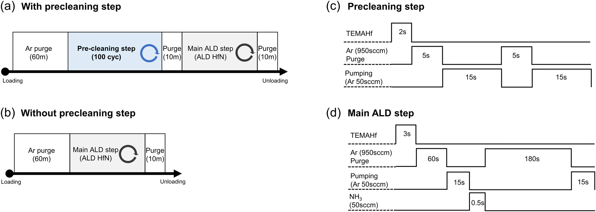 | ||
| Fig. 1 Atomic layer deposition(ALD) process flow of HfNx from substrate loading to unloading, (a) with and (b) without the precleaning step. Pulse time and Ar flow of one cycle of (c) precleaning step and (d) main ALD step. | ||
One cycle of the precleaning step consisted of injecting TEMAHf for 2 s, Ar purging with 950 sccm for 5 s, and another Ar purging with 50 sccm for 15 s twice, as shown in Fig. 1(c). A consecutive pulse of Ar with various flow rates was included to ensure the extraction of the remaining TEMAHf precursor, oxygen, from the chamber. The main HfNx ALD cycle was composed of pulsing TEMAHf for 3 s, Ar pur ging with 950 sccm for 60 s + 50 sccm for 15 s, NH3 gas pulse (50 sccm) for 0.5 s, and Ar purging with 950 sccm for 180 s + 50 sccm for 15 s, as shown in Fig. 1(d).
Fig. 2(a–d) shows variations in the growth per cycle (GPC) of the HfNx film with the change in the ALD parameters. All the HfNx films were grown with the precleaning step. Self-limiting behavior, a typical characteristic of ALD, was observed for precursor injection and purge times. The times of the four steps constituting the ALD process are displayed inside each graph (precursor feeding time/Ar purge time/NH3 feeding time/Ar purge time; ‘X’ represents a variable). Fig. 2(a) shows the change in GPC with increasing TEMAHf injection time. The increase rate of GPC decreased at 1 s of TEMAHf injection time and was saturated after 3 s. Fig. 2(b) shows the GPC variation as the NH3 injection time increases. The GPC was saturated even at 0.5 s. The saturated GPC was 0.135 nm per cycle for both the TEMAHf and NH3 injections. Fig. 2(c and d) show the GPC with increasing purge time of the two purge steps. It was found that a purge time of more than 60 s (or 180 s) is required to sufficiently remove the excess TEMAHf precursor (or byproducts formed by the reaction with NH3 gas). Previous papers reported that NH3 forms non-volatile adducts during deposition,18 requiring a more extended purge to remove such byproducts. Based on these results, the ALD cycle of the HfN film consisted of the following steps with an intermittent pumping step (Ar 50 sccm) for 15 s after each purge step (see Fig. 1(d)): TEMAHf feeding (3 s), Ar purge (60 s), NH3 feeding (0.5 s), and Ar purge (180 s).
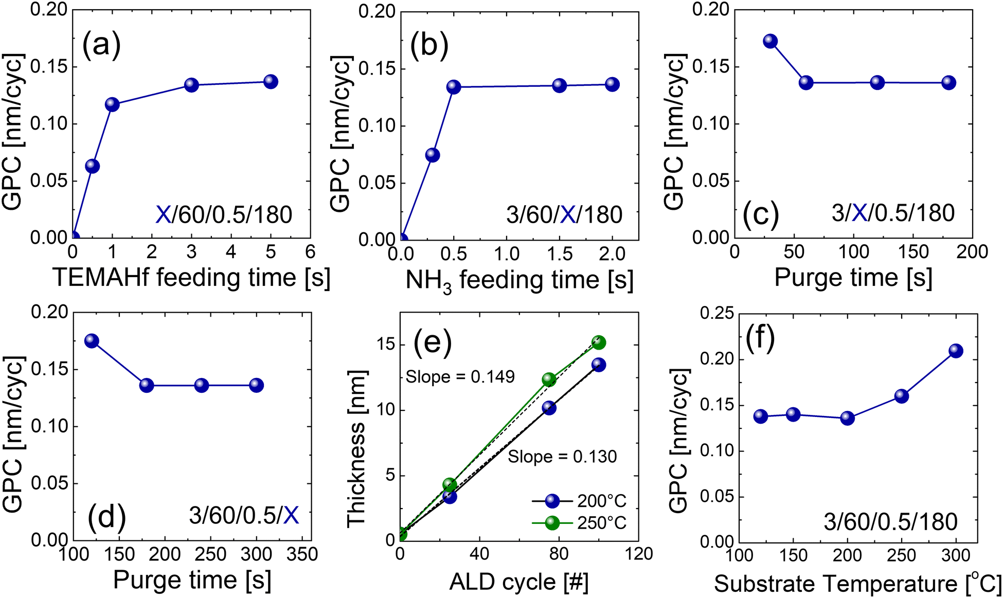 | ||
| Fig. 2 Variation of growth per cycle (GPC) of HfNx, deposited with the precleaning step, with the change in (a) Hf[N(CH3)(C2H5)]4 (TEMAHf) feeding time, (b) NH3 feeding time, (c) TEMAHf purge time, and (d) NH3 purge time. (e) Increasing thickness of HfNx film with ALD cycle at different temperature, and (f) change in HfNx GPC with increasing substrate temperature. | ||
Fig. 2(e) shows that the thickness linearly increases as the ALD cycle numbers increase. High linearity was observed with almost no incubation cycles. The GPC calculated by the slope was ∼0.130 nm per cycle, which agrees with the saturated growth rate shown in Fig. 2(a–d). Fig. 2(f) shows the GPC with increasing deposition temperatures. An ALD window with a constant GPC was observed between 120 and 200 °C, but the higher growth temperatures (>250 °C) increased the GPC, suggesting the thermal decomposition of the precursor. It has been reported that TEMAHf starts to thermally decompose from 250 °C to 300 °C.19,20
Effect of the precleaning step on the impurity concentration of HfNx film
Fig. 3(a and b) show the AES depth profiles of the 15 nm-thick HfNx films without and with the precleaning step, respectively, and Fig. 3(c and d) show the schematic diagrams for the deposition process of the corresponding films. The film without the precleaning step had an oxygen concentration as high as ∼40–60%, and the chemical composition was non-uniform across the film thickness. Even though the chamber was purged with Ar gas for 1 hour before the onset of the main ALD cycles, oxygen impurities were not effectively removed from the ALD chamber. In addition, although the NH3 gas concentration must be higher than that of oxygen impurities near the substrate when injecting NH3, the much higher reactivity of Hf atoms (or TEMAHf molecules) toward oxygen-containing species than NH3 oxidized the growing film. Therefore, the film was vulnerable to oxidation, as shown in Fig. 3(c).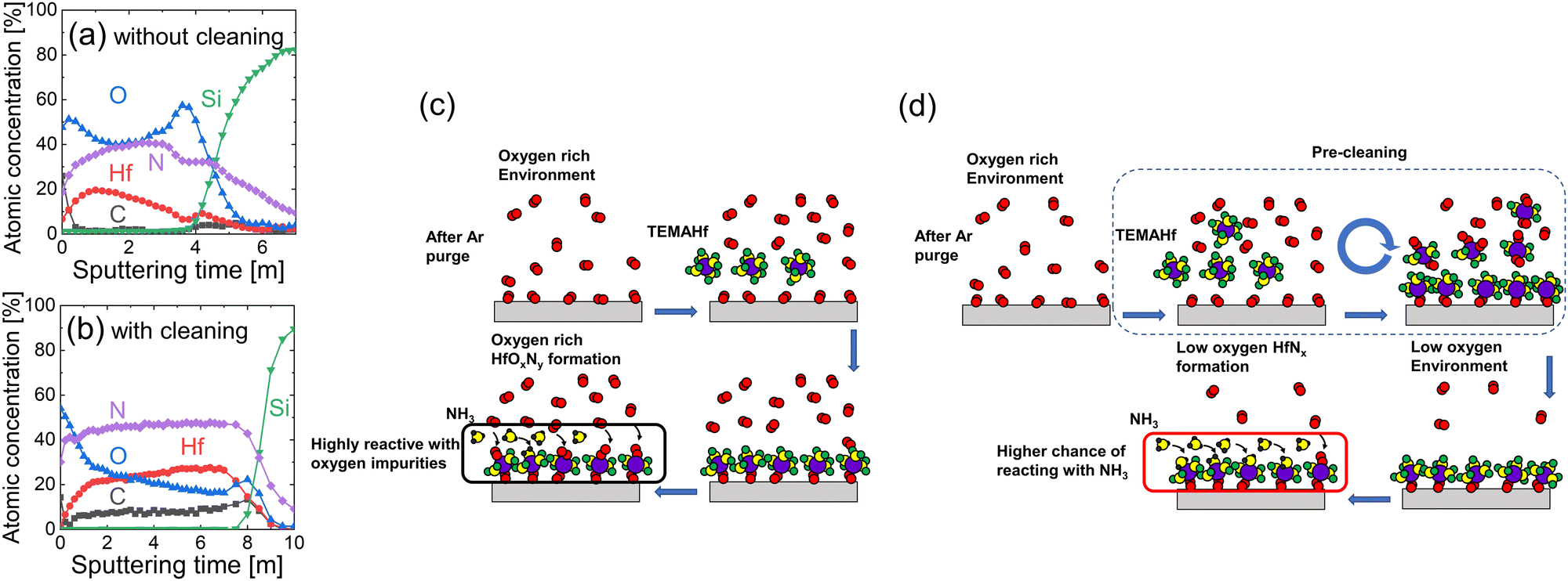 | ||
| Fig. 3 Auger electron spectroscopy depth profile of 15 nm HfNx film deposited (a) without and (b) with a cleaning step and flowchart illustrating how the films are deposited (c) without and (d) with cleaning step. | ||
Moreover, the high oxidation potential of TEMAHf could be utilized to remove the oxygen-containing species within the ALD chamber in the precleaning step. The TEMAHf precursor, which may react with the oxygen-containing species on the substrate surface, within the chamber volume, and on the inner surface, was injected without the NH3. The subsequent Ar purge and pumping cycles removed the reaction byproducts and unreacted TEMAHf molecules, as shown in the upper schematics of Fig. 3(d). Because of including such a precleaning step, the oxygen concentration in the deposited film decreased to <∼20% (Fig. 3(b)). The high surface oxygen concentration was owing to the adverse oxidation of the film during the air exposure before the AES analysis. Additionally, the chemical composition of the film became more uniform. However, the carbon impurity concentration increased to ∼8%, indicating relatively lower reactivity of NH3 compared with the oxygen or water molecules during the ALD (Lower panel schematics of Fig. 3(d)). However, post-annealing in the NH3 ambient could decrease these unwanted oxygen and carbon concentrations, as shown later.
The TEMAHf molecules injected during the precleaning step grew an additional thickness of only ∼0.6 nm, which could be identified from the y-axis intercept, as demonstrated in Fig. 2(e).
Fig. S1(a) of the online ESI† shows that thickness increases as a function of the ALD cycle number. All samples were deposited without the precleaning step. Fig. S1(b–d) (ESI†) shows the AFM and SEM images of TiN before and after the precleaning step. Compared to the thickness increase of HfNx film deposited with the precleaning step in Fig. 2(e), GPC remained almost constant (0.125 nm per cycle), but an incubation cycle of ∼16 cycles was observed. Therefore, some of the precursors are adsorbed on the substrate during the precleaning step, which enhances precursor adsorption for subsequent film growth, thereby eliminating the incubation cycle.
The roughness increased from 0.29 nm to 0.34 nm after the precleaning step owing to TEMAHf precursor adsorption, which coincides with the results illustrated in Fig. S1(a) (ESI†). The grain diameter of TiN increased from 6.58 nm to 7.01 nm after the precleaning step.
Annealing effect on the films deposited with the precleaning step
To further lower the oxygen concentration in the HfNx films and to remove carbon impurities caused by the precleaning step, annealing was carried out at 900 °C in an N2 or NH3 gas atmosphere for 60 s. Fig. 4(a and b) show the AES depth profile of HfNx films annealed in N2 and NH3 gas atmospheres, respectively. All the HfNx films were grown with the precleaning step. The annealing in the N2 gas atmosphere decreased the carbon concentration from ∼8% to ∼4%. However, it slightly increased the oxygen concentration, which may have been caused by the residual oxygen concentration in the N2 gas.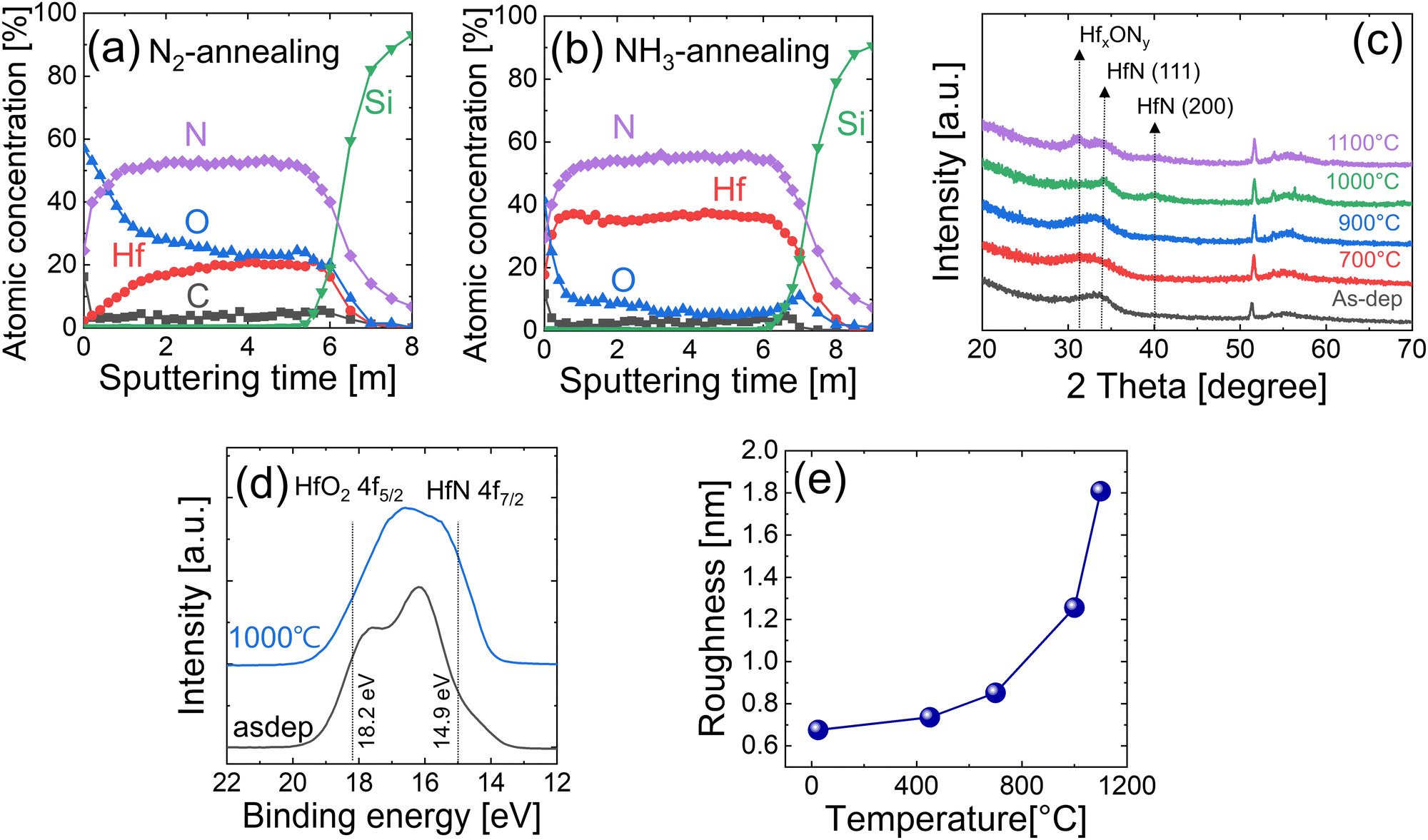 | ||
| Fig. 4 AES depth profile of the HfNx film annealed at 900 °C with (a) N2 and (b) NH3 ambient. (c) Grazing-angle incidence X-ray diffraction (GIXRD) analysis of films annealed at various temperatures, X-ray photoelectron spectroscopy of films annealed at various temperatures, and (e) roughness. All films were deposited with the precleaning step, with a thickness of 15 nm, and annealing was conducted in NH3 ambient, except for (a). | ||
In contrast, the annealing in the NH3 atmosphere almost completely removed the carbon impurity (<2% of residual concentration). Notably, oxygen impurities were significantly reduced to ∼5% in the bulk film. The relatively high oxygen concentration near the surface is due to adverse oxidation during air exposure. NH3 gas has a higher chemical reactivity for nitridation than N2. Therefore, when HfNx film is annealed under the NH3 atmosphere, NH3 protects the thin film from oxidation and replaces loosely bonded oxygen and carbon impurities with nitrogen.
Fig. 4(c) shows the GIXRD spectra of the films as-deposited and annealed under the NH3 atmosphere for 60 s at various temperatures (700–1100 °C). The broad peak at 2θ = 30–35° of the as-deposited film was attributed to HfNx (x > 1) in previous studies that reported ALD14 and chemical vapor deposition (CVD) of HfNx films.17 They also adopted TEMAHf and NH3, as in this study, and reported that the deposited film had a similar composition to the Hf3N4 instead of HfN.14 Phase transformation from HfNx did not occur even when the films were annealed at 900 °C, showing a similar GIXRD pattern to the as-deposited sample. However, when the film was annealed at 1000 °C, HfN (111) and HfN (200) peaks appeared, suggesting the crystallization of the film into the HfN phase. This result resembles the experimental result of Wang et al.,17 where the phase change from HfNx (x > 1) to the HfN phase was observed when the film was heat treated above 950 °C under the vacuum condition (10−5 Pa). When the annealing temperature was further increased to 1100 °C, oxygen contamination in the RTP chamber or the remaining oxygen impurities in the film reacted with the HfN, showing an HfOxNy peak near 2θ = ∼32°.
Fig. 4(d) shows the XPS Hf 4f spectra of the 15 nm-thick films, which were as-deposited and post-annealed at 1000 °C under the NH3 atmosphere. A thin surface layer (3 nm) was in situ etched by Ar+ ions in the XPS chamber to remove the surface oxidation layer by air exposure. Because there are various oxynitrides (HfOxNy) as well as oxide (HfO2) and nitride (HfN, Hf3N4) inside the film, the deconvolution of each peak was challenging. Therefore, the two XPS spectra were compared based on the standard Hf 4f peak positions of the HfO2 and HfN phases. Because the electronegativity of oxygen is higher than that of nitrogen, the binding energy of Hf 4f electrons in oxides is higher than that of nitrides.21–25 Moreover, the binding energy of Hf 4f in Hf3N4 is higher than that in HfN. Therefore, the highest and lowest binding energy peaks that the HfNx thin films can show are the Hf 4f5/2 peak of HfO2 and the Hf 4f7/2 peak of HfN, respectively.
The as-deposited film showed relatively well-separated peaks, with its higher binding energy peak position being consistent with the Hf 4f5/2 peak of HfO2. However, compared with the as-deposited film, the XPS spectra of the annealed HfNx film showed a non-separated peak, and its position shifted toward the low binding energy direction. In addition, the intensity was notably increased near 14.9 eV, which corresponded to the HfN 4f7/2 peak. This finding indicates that oxygen was released from the film when the film was annealed, and the oxidation state of Hf transformed from 4+ to 3+ state, showing an increase in HfN bonding.
Fig. 4(e) shows the variations in the surface roughness of the 15 nm-thick films annealed at various temperatures, estimated by the AFM. The AFM images are shown in Fig. S2 (ESI†). Roughness increased with increasing temperature but did not show a substantial change until the annealing temperature increased to 1000 °C. Above 1000 °C, it significantly increased as the film crystallized (Fig. 4(c)). Fig. S3 (ESI†) shows the SEM images of the corresponding samples. The film showed smooth and fine-grained surface morphologies of up to 700 °C, and a notable increase in grain size of over 1000 °C. When the film was crystallized by the RTA at >900 °C, the grain diameter was ∼7–8 nm.
To determine the conformity of the ALD deposition, HfN was deposited on a contact hole structure with an opening diameter and depth of 54.8 and 385.7 nm, respectively (aspect ratio is ∼1![[thin space (1/6-em)]](https://www.rsc.org/images/entities/char_2009.gif) :7). Fig. 5(a) shows the cross-section of the hole structure filled with the as-deposited HfNx film observed by the Cs-STEM. The entire contact hole region was filled with the film, and only a tiny seam could be observed at the center portion, suggesting conformal film growth. Fig. 5(b) shows the Cs-TEM image of the red square area in Fig. 5(a and c) shows the fast-Fourier transformed (FFT) image of the red area in Fig. 5(b). The film showed no evidence of crystallization, but Fig. 5(c) shows broad rings and faint spots, suggesting the inclusion of sub-nano-scale crystalline nuclei. This finding agrees with the broad GIXRD peak from the as-deposited, as shown in Fig. 4(c).
:7). Fig. 5(a) shows the cross-section of the hole structure filled with the as-deposited HfNx film observed by the Cs-STEM. The entire contact hole region was filled with the film, and only a tiny seam could be observed at the center portion, suggesting conformal film growth. Fig. 5(b) shows the Cs-TEM image of the red square area in Fig. 5(a and c) shows the fast-Fourier transformed (FFT) image of the red area in Fig. 5(b). The film showed no evidence of crystallization, but Fig. 5(c) shows broad rings and faint spots, suggesting the inclusion of sub-nano-scale crystalline nuclei. This finding agrees with the broad GIXRD peak from the as-deposited, as shown in Fig. 4(c).
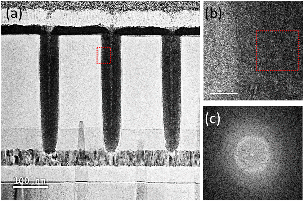 | ||
| Fig. 5 (a) Cs-corrected scanning transmission electron microscopy (Cs-STEM) image of HfNx film deposited on contact hole structure with an aspect ratio of 1:7, (b) Cs-corrected TEM image of red square area in (a) and (c) fast-Fourier transformed image of red box area in (b). | ||
Annealing effect on the films deposited without the precleaning step
Fig. 6(a) shows the GIXRD spectra of the films deposited without the precleaning step, which are annealed under the NH3 atmosphere for 60 s at various temperatures (700–1000 °C). As-deposited films showed similar characteristics to films deposited with the precleaning step, having broad peaks at 2θ = 30–35°. The film annealed at 700 °C showed intense peaks that could not be assigned to HfO2, Hf3N4, or HfN. When the chemical composition of mixed oxide and nitride under this growth condition was considered, these peaks could be reasonably assigned to the HfOxNy phase. The crystallization temperature of hafnium oxides with a thickness of 10–20 nm is in the range of 400–700 °C,26–29 which is below the phase transformation temperature of Hf3N4 to HfN. Therefore, the higher oxygen concentration of the grown film without the precleaning step may induce crystallization even at 700 °C.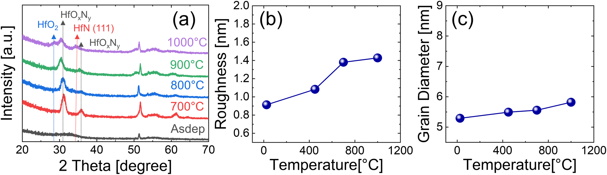 | ||
| Fig. 6 (a) GIXRD, (b) roughness, and (c) grain diameter dependence on the annealing temperature of 15nm HfNx films deposited without the precleaning step. All samples were annealed at NH3 ambient. | ||
It is notable that increasing the RTA temperature up to 900 °C shifted the HfOxNy peak to a lower angle and decreased the diffraction peak intensities. This behavior could be explained by the gradual elimination of oxygen from the film as the RTA temperature increases, which must be accompanied by decreased crystallization since crystallization into the nitride has not occurred. At 1000 °C, the film crystallized into a mixture of HfO2 and HfN. Fig. 6(b and c) show the roughness and grain size changes with the RTA temperature, respectively. The raw AFM and SEM images for these values are included in Fig. S4 and S5 of ESI,† respectively. They increased insignificantly to 1000 °C, in contrast to the samples deposited with the precleaning process, because the film was already crystalline even at 700 °C. The grain diameter was smaller than that of the annealed films deposited with the precleaning step.
Therefore, it can be concluded that NH3 annealing effectively decreases the oxygen concentration in the as-deposited film. However, the precleaning step is required for high-quality nitride film growth. If not, even after RTA in the NH3 atmosphere, the film will eventually crystallize into a mixture of oxide and nitride.
Electrical properties of films deposited with the precleaning step
The electrical properties of 15 nm-thick as-deposited and annealed films deposited with the precleaning step were investigated. Fig. 7(a) shows the J–V curves of the films, indicating that the as-deposited and annealed films up to 700 °C are insulating. This finding agrees with the phase analysis in Fig. 4(c), where the change to conducting HfN did not appear up to an annealing temperature of 900 °C. However, the film annealed at 1000 °C showed a very high current density, corroborating the evolution of the HfN phase at this temperature (Fig. 4(c)). The film resistivity was estimated using the four-point probe method, and the results are summarized in Fig. 7(b). The as-deposited film and the films annealed below 900 °C were too insulating to measure their resistivity values by applying the given method. When the film was annealed at 950 °C, its resistivity was as high as ∼3 × 10⁷ μΩ cm, suggesting the incomplete transition into the conducting HfN phase. When the annealing temperature increased to 1000 °C, the resistivity decreased to ∼1 × 10⁶ μΩ cm, suggesting more HfN formation. However, a further resistivity decrease was not observed with an even higher annealing temperature, which agrees with the results of Wang et al.17 The 1 × 10⁶ μΩ cm of resistivity is significantly larger than the bulk resistivity of HfN (33 μΩ cm). This high resistivity indicates the presence of an untransformed Hf3N4 phase and the involvement of insulating oxides, which can be observed in the broad XPS peak shown in Fig. 4(d).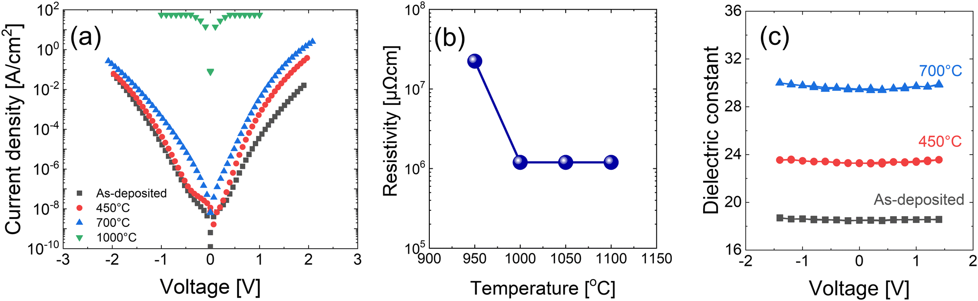 | ||
| Fig. 7 (a) Current density–voltage graph, (b) resistivity, and (c) dielectric constant–voltage analysis of 15 nm HfNx films annealed at various temperatures under NH3 ambient. | ||
The dielectric constant of the insulating HfNx was measured through C–V measurements. Fig. 7(c) shows the dielectric constant of 15 nm-thick films with various annealing temperatures. As shown in Fig. S6 of ESI,† the dielectric loss was sufficiently low (<0.02) to ensure the reliability of capacitance. The dielectric constant of the as-deposited film was ∼19 and increased to ∼30 when annealed at 700 °C. Because the dielectric constants of HfO2 and Hf3N4 are ∼15–20 and ∼31,30 respectively, the increment in the dielectric constant with temperature is caused by the removal of oxygen in the film, which occurs more effectively at a higher temperature.
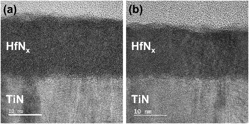
Fig. 8(a and b) show the Cs-STEM images of HfNx annealed at 450 °C and 700 °C, respectively. They show that the interfacial layer between TiN and HfN does not differ with the annealing temperature. However, the film after 700 °C annealing shows local crystallization, which may contribute to the dielectric constant increase.
 | ||
| Fig. 8 Cs-STEM image of HfNx annealed at (a) 450 °C and (b) 700 °C. All films were deposited with pre-cleaning step. | ||
Conclusions
Thermal ALD of the HfNx film was attempted using TEMAHf and NH3 as the Hf- and N-sources, respectively, at a typical substrate temperature of 200 °C. Although the adopted precursor and reactant showed a facile ALD reaction route via the ligand exchange reaction, the residual oxygen-containing species, O2 and H2O, in the reaction chamber severely contaminated the film with oxygen. The problem could not be solved even with a prolonged Ar purge step. Therefore, an in situ precleaning step was devised to eliminate the adverse oxygen-containing species within the ALD chamber after loading the substrate. This precleaning step was composed of repeated pulsing and purging of the TEMAHf precursor without introducing NH3 gas. The precleaning step resulted in minimal film (perhaps HfOx) growth (∼0.6 nm) on the substrate but substantially decreased the oxygen concentration in the film from 40–50% to ∼20%. The ALD-specific saturated growth was confirmed with a saturated growth per cycle of ∼0.13 nm per cycle.However, the lower chemical reactivity of NH3 toward the TEMAHf precursor, compared with oxygen-containing species, resulted in relatively high oxygen (∼20%) and carbon contamination (∼8%). Therefore, post-deposition RTA under the NH3 atmosphere further decreased the oxygen and carbon contents. The post-annealing at temperatures higher than 900 °C efficiently decreased the oxygen and carbon concentrations to ∼5% and 2%, respectively. However, crystallization into the conducting HfN layer was achieved after annealing at temperatures higher than 1000 °C. The resistivity of the crystallized film was ∼1 × 10⁶ μΩ cm, which is 4–5 orders of magnitude higher than the bulk HfN. Such a higher resistivity and high annealing temperature (>1000 °C) render the ALD HfNx film inappropriate as the electrode for HfO2-based dielectric and ferroelectric films. Instead, it may be useful as the buffer layer to suppress the adverse chemical interaction between the dielectric/ferroelectric film and TiN electrode, which was reported for the sputter-deposited HfOxNy film.
Author contributions
S. K. R. and B. Y. K. contributed equally to this study.Conflicts of interest
There are no conflicts to declare.Acknowledgements
This work was supported by the National Research Foundation of Korea (No. 2020R1A3B2079882).References
- U. Schroeder, M. H. Park, T. Mikolajick and C. S. Hwang, Nat. Rev. Mater., 2022, 1–17 Search PubMed.
- M. Hyuk Park, H. Joon Kim, Y. Jin Kim, W. Lee, H. Kyeom Kim and C. Seong Hwang, Appl. Phys. Lett., 2013, 102, 112914 CrossRef.
- M. Hyuk Park, H. Joon Kim, Y. Jin Kim, T. Moon and C. Seong Hwang, Appl. Phys. Lett., 2014, 104, 072901 CrossRef.
- S. J. Kim, J. Mohan, S. R. Summerfelt and J. Kim, JOM, 2019, 71, 246–255 CrossRef CAS.
- M. H. Park, H. J. Kim, Y. J. Kim, W. Jeon, T. Moon and C. S. Hwang, Phys. Status Solidi RRL, 2014, 8, 532–535 CrossRef CAS.
- M. H. Park, H. J. Kim, Y. J. Kim, W. Lee, T. Moon, K. D. Kim and C. S. Hwang, Appl. Phys. Lett., 2014, 105, 072902 CrossRef.
- W. Hamouda, A. Pancotti, C. Lubin, L. Tortech, C. Richter, T. Mikolajick, U. Schroeder and N. Barrett, J. Appl. Phys., 2020, 127, 064105 CrossRef CAS.
- B. Y. Kim, S. H. Kim, H. W. Park, Y. B. Lee, S. H. Lee, M. Oh, S. K. Ryoo, I. S. Lee, S. Byun and D. Shim, Appl. Phys. Lett., 2021, 119, 122902 CrossRef CAS.
- B. Y. Kim, H. W. Park, S. D. Hyun, Y. B. Lee, S. H. Lee, M. Oh, S. K. Ryoo, I. S. Lee, S. Byun and D. Shim, Adv. Electron. Mater., 2022, 8, 2100042 CrossRef CAS.
- S. J. Kim, J. Mohan, H. S. Kim, S. M. Hwang, N. Kim, Y. C. Jung, A. Sahota, K. Kim, H.-Y. Yu and P.-R. Cha, Materials, 2020, 13, 2968 CrossRef CAS PubMed.
- S. Consiglio, W. Zeng, N. Berliner and E. T. Eisenbraun, J. Electrochem. Soc., 2008, 155 Search PubMed.
- S. Karwal, M. A. Verheijen, B. L. Williams, T. Faraz, W. M. M. Kessels and M. Creatore, J. Mater. Chem. C, 2018, 6, 3917–3926 RSC.
- W. Jeong, Y. Ko, S. Bang, S. Lee and H. Jeon, J. Korean Phys. Soc., 2010, 56, 905–910 CrossRef CAS.
- J. S. Becker, E. Kim and R. G. Gordon, Chem. Mater., 2004, 16, 3497–3501 CrossRef CAS.
- B. Thapa, R. Patterson, M. Dubajic, G. Conibeer and S. Shrestha, 2019 IEEE 46th Photovoltaic Specialists Conference (PVSC), 2019, 1797–1801 Search PubMed.
- G. L. Humphrey, J. Am. Chem. Soc., 1953, 75, 2806–2807 CrossRef CAS.
- W. Wang, T. Nabatame and Y. Shimogaki, Jpn. J. Appl. Phys., 2006, 45, L1183 CrossRef CAS.
- D. A. Neumayer and J. G. Ekerdt, Chem. Mater., 1996, 8, 9–25 CrossRef CAS.
- N. K. Oh, J.-T. Kim, J.-K. Ahn, G. Kang, S. Y. Kim and J.-Y. Yun, Appl. Sci. Convergence Technol., 2016, 25, 56–60 CrossRef.
- S. Heil, J. Van Hemmen, C. Hodson, N. Singh, J. Klootwijk, F. Roozeboom, M. Van de Sanden and W. Kessels, J. Vac. Sci. Technol., A, 2007, 25, 1357–1366 CrossRef CAS.
- S. Karwal, M. Verheijen, B. Williams, T. Faraz, W. Kessels and M. Creatore, J. Mater. Chem. C, 2018, 6, 3917–3926 RSC.
- A. Perry, L. Schlapbach and W. Sproul, Solid State Commun., 1987, 62, 23–26 CrossRef CAS.
- A. Arranz and C. Palacio, Surf. Sci. Spectra, 2004, 11, 33–42 CrossRef CAS PubMed.
- W. Wang, T. Nabatame and Y. Shimogaki, Surf. Sci., 2005, 588, 108–116 CrossRef CAS.
- C. S. Kang, H.-J. Cho, K. Onishi, R. Nieh, R. Choi, S. Gopalan, S. Krishnan, J. H. Han and J. C. Lee, Appl. Phys. Lett., 2002, 81, 2593–2595 CrossRef CAS.
- D. Biswas, M. N. Singh, A. K. Sinha, S. Bhattacharyya and S. Chakraborty, J. Vac. Sci. Technol., B: Nanotechnol. Microelectron.: Mater., Process., Meas., Phenom., 2016, 34, 022201 Search PubMed.
- X.-Y. Zhang, C.-H. Hsu, S.-Y. Lien, W.-Y. Wu, S.-L. Ou, S.-Y. Chen, W. Huang, W.-Z. Zhu, F.-B. Xiong and S. Zhang, Nanoscale Res. Lett., 2019, 14, 1–8 CrossRef PubMed.
- T. Böscke, J. Müller, D. Bräuhaus, U. Schröder and U. Böttger, Appl. Phys. Lett., 2011, 99, 102903 CrossRef.
- M. Vargas, N. Murphy and C. Ramana, Opt. Mater., 2014, 37, 621–628 CrossRef CAS.
- T. Ino, Y. Kamimuta, M. Suzuki, M. Koyama and A. Nishiyama, Jpn. J. Appl. Phys., 2006, 45, 2908 CrossRef CAS.
Footnote |
| † Electronic supplementary information (ESI) available. See DOI: https://doi.org/10.1039/d2tc03964h |
| This journal is © The Royal Society of Chemistry 2023 |