
 Open Access Article
 This Open Access Article is licensed under a
 Creative Commons Attribution 3.0 Unported Licence
Highly conductive and long-term stable films from liquid-phase exfoliated platinum diselenide†
Kangho
Lee
 a,
Beata M.
Szydłowska
ab,
Oliver
Hartwig
a,
Kevin
Synnatschke
c,
Bartlomiej
Tywoniuk
a,
Tomáš
Hartman
d,
Tijana
Tomašević-Ilić
e,
Cian P.
Gabbett
c,
Jonathan N.
Coleman
c,
Zdeněk
Sofer
d,
Marko
Spasenović
f,
Claudia
Backes
bg and
Georg S.
Duesberg
*a
a,
Beata M.
Szydłowska
ab,
Oliver
Hartwig
a,
Kevin
Synnatschke
c,
Bartlomiej
Tywoniuk
a,
Tomáš
Hartman
d,
Tijana
Tomašević-Ilić
e,
Cian P.
Gabbett
c,
Jonathan N.
Coleman
c,
Zdeněk
Sofer
d,
Marko
Spasenović
f,
Claudia
Backes
bg and
Georg S.
Duesberg
*a
aInstitute of Physics, EIT 2, Faculty of Electrical Engineering and Information Technology, University of the Bundeswehr Munich & SENS Research Center, Werner-Heisenberg-Weg 39, 85577, Neubiberg, Germany. E-mail: duesberg@unibw.de
bInstitute of Physical Chemistry, Heidelberg University, 69120, Heidelberg, Germany
cSchool of Physics, CRANN & AMBER Research Centres, Trinity College Dublin, Dublin 2, Ireland
dDepartment of Inorganic Chemistry, University of Chemistry and Technology Prague, Technicka 5, 166 28, Prague 6, Czech Republic
eInstitute of Physics Belgrade, University of Belgrade, Pregrevica 118, 11080, Belgrade, Serbia
fCenter for Microelectronic Technologies, Institute of Chemistry, Technology and Metallurgy, University of Belgrade, Njegoševa 12, 11000, Belgrade, Serbia
gPhysical Chemistry of Nanomaterials, University of Kassel, Heinrich-Plett-Str. 40, 34132, Kassel, Germany
First published on 16th December 2022
Abstract
Liquid-phase exfoliation (LPE) has been introduced as a versatile and scalable production method for two-dimensional (2D) materials. This method yields dispersions that allow for the fabrication of printable and flexible electronic devices. However, the fabrication of uniform and homogeneous films from LPE dispersions with a performance similar to that of bottom-up grown materials remains a challenge, as the film quality strongly influences the optical and electrical performance of devices. Furthermore, long-term stability remains a major challenge for all 2D material based applications. In this study, we report on highly conductive tiled network films made of platinum diselenide (PtSe2) flakes derived using a scalable LPE method. We characterized the homogeneous films in terms of morphology and electrical behavior. As an example of applicability, we produce a chemiresistive sensor structure with the PtSe2 films and show significant resistance changes upon periodic ammonia gas exposures, revealing a sub-0.1 part per million (ppm) detection limit (DL). More remarkably the devices are fully functional after 15 months, underlining the high stability of PtSe2 based devices.
Introduction
The unique properties of two-dimensional (2D) materials that enable high potential for their employment in numerous applications have led to enormous scientific interest.1–3 In particular, they have been proposed for chemical sensing due to their high surface-area-to-volume ratio. Graphene-based sensors have shown ultimate sensitivity, detecting even individual gas molecules4 while 2D transition metal dichalcogenide (TMD) materials showed extreme sensitivities to trace gases.5–13 In particular, PtSe2 has been shown to have superior gas sensitivity,11 and gas selectivity was predicted by density functional theory.14 Moreover, the outstanding electrochemical properties of platinum chalcogen compounds show promise for further applications.15,16Within the toolset for the production of these materials, liquid phase exfoliation (LPE) has been proposed as a means for achieving high volume and yield. LPE has been used to exfoliate a range of 2D materials including graphite,17–22 boron nitride,23,24 pnictogens,25–30 TMDs,24,31–37 III–V semiconductors,38 metal oxides,39–41 and many others.42–47 LPE is used to produce 2D materials in liquid dispersions, which can be used as inks, making the method attractive for various printing technologies, which allow for the fabrication of flexible devices or back end of line (BEOL) integration with existing integrated chips.24,48 Most recently we were able to report on LPE-PtSe2.49
Methods for producing films from LPE materials include vacuum filtration,17,19 Langmuir–Blodgett (LB) deposition,50–54 spray-coating55 and inkjet printing.56 However, many of these methods suffer from flake reaggregation into clusters in solution and on the substrate, leading to inhomogeneous films. In order to compensate for this, extra layers of materials must be added resulting in thick films (>1 μm) which is detrimental in numerous applications and significantly increases production costs. Therefore, the formation of very thin homogenous films from LPE materials is not only crucial to the electrical and optical performance of devices, but is also a determining factor in the applicability of production methods.
Here we report for the first time film formation from PtSe2 dispersions using a modified LB method at a liquid–liquid interface. Homogeneous films with low roughness and controllable thickness could be produced. These films were characterized using Raman spectroscopy, atomic force microscopy (AFM), and scanning electron microscopy (SEM) and compared to the conventional spray-deposited films. We contacted the LB films with interdigitated electrodes for electrical characterization. In a simple chemiresistive sensor structure, we show high sensitivity and fast response upon exposure to ammonia (NH3) gas. Notably, we demonstrate the long-term stability of our films over 15 months.
Experimental
Synthesis of bulk crystals
Platinum sponge (Pt 99.99%, Surepure Chemetals) and selenium (Se 99.9999%, granules 2–4 mm, Wuhan Xinrong New Materials Co.) were placed in a quartz ampoule and sealed by an oxygen–hydrogen welding torch at a pressure of 1 mPa. Selenium was used in 2 at% excess. The ampoule was heated at 1270 °C in a 5 °C per minute of ramping speed and cooled down to 1000 °C at a 1 °C per minute of cooling rate after 30 minutes of dwell time. Afterwards, it was completely cooled down to room temperature. The selenium excess condensed on the opposite side of the ampoule, and the formed crystalline block of PtSe2 was removed from the ampoule.Preparation of the dispersions
The PtSe2 dispersions were prepared using our previously established methodology of tip sonication and size selection by centrifugation in aqueous sodium cholate solution57 followed by transfer to N-methyl-2-pyrrolidone (NMP) to aid the deposition at the liquid–liquid interface. PtSe2 crystals were ground and immersed in 35 mL of aqueous sodium cholate (SC) solution (concentrations: CPtSe2 = 0.5 g L−1 and CSC = 1.7 g L−1) and ultrasonicated (Sonics VXC500, 500 W, equipped with a tapered microtip) for 7.5 hours at 30% amplitude with a pulse of 6 seconds on and 4 seconds off. The dispersion was kept in a 4 °C cooling cell during sonication to avoid heating. The polydispersity of the as-produced dispersion was reduced by two consecutive centrifugation runs. High mass nanosheets which are larger and simultaneously thicker were discarded as sediment after the first run at lower centrifugal acceleration, while smaller/thinner nanosheets were removed as the supernatant after the second step at higher centrifugal acceleration. Specifically, unless otherwise noted, centrifugation was performed in a Hettich Mikro 220R centrifuge for 2 hours at 13 °C. The first step at a relative centrifugal force of 3000g (where g denotes the earth's gravitational field) was carried out with a fixed-angle rotor 1016 in 50 mL centrifuge tubes filled with ∼17 mL each. The supernatant was decanted and subjected to a second centrifugation at 5000g (with a fixed-angle rotor 1995-A in 1.5 mL Eppendorf tubes) after which the sediment was collected in deionized (DI) water and the supernatant discarded.Preparation of films
Films were deposited after pre-assembly of the nanosheets at the liquid–liquid interface. First, the aqueous dispersion was transferred to NMP. To this end, the dispersion was centrifuged at 6000g (2 hours) to force the nanosheets to sediment and the sediment was redispersed in isopropanol (IPA) by bath-sonication for 5 minutes. The aqueous supernatant containing mostly water/surfactant was discarded. The centrifugation was repeated, the supernatant containing residual water and IPA was discarded and the sediment redispersed in NMP by 5 minutes of bath sonication. As substrates, SiO2/Si wafers were chosen with an oxide thickness of 300 nm. These were diced to a size of 15 by 7.5 mm2, cleaned by bath sonication in acetone, IPA, ethanol, and water for 20 min in each solvent and subsequently dried under a stream of pressured nitrogen. Fig. 1 depicts a schematic of the controlled deposition of PtSe2 nanosheets on a SiO2/Si substrate. Overall, the procedure can be regarded as a LB type deposition using two immiscible solvents, in this case water and toluene. It has been demonstrated that nanoflakes can be trapped at the liquid–liquid interface when injecting the LPE dispersion at an angle close to 90° with respect to the interface.58,59 To form the liquid–liquid interface, first, a 15 mL glass beaker was filled with 12 mL of DI water and 0.5 mL of toluene was layered on top. Next, 0.1 mL of the PtSe2 dispersion in NMP were gently injected on top and allowed to rest for 3 minutes to allow diffusion of the nanosheets to the toluene/water interface. After a uniform layer was formed, the toluene was allowed to evaporate and subsequently the transfer to the substrate was performed. To this end, the substrate was vertically introduced into the water phase, then tilted to an angle near 90° relative to the interface and then lifted up manually with a tweezer at speeds as constant as possible.60 Generally, a smaller angle between the substrate and film is more favorable for the film transfer. Finally, the film was left to dry in air for ∼15 min with a tilt angle of ∼30° before performing a washing step by rinsing the films gently with a 1![[thin space (1/6-em)]](https://www.rsc.org/images/entities/char_2009.gif) :1 mixture of IPA and DI water. Excess of unnecessary film area was removed by gently scraping with a cotton swab, leaving an area of approximately 5 by 5 mm2 in the center of the substrate.
:1 mixture of IPA and DI water. Excess of unnecessary film area was removed by gently scraping with a cotton swab, leaving an area of approximately 5 by 5 mm2 in the center of the substrate.
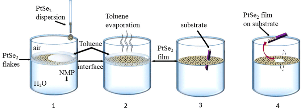 | ||
| Fig. 1 Schematic of the modified Langmuir–Blodgett method to produce tiled nanosheet networks after pre-assembly at a liquid–liquid interface (1-film formation, 2-interface area reduction by evaporation, 3-substrate immersion, and 4-film deposition). | ||
Characterization
Scanning electron microscopy (SEM) characterization was performed with a JEOL JSM-6700F field emission SEM at 1 kV of acceleration voltage. Raman characterization was performed by mapping a region of 50 by 50 μm2 with 100 measurement spots with a Witec alpha300 R confocal Raman microscope at an excitation wavelength of 532 nm at 0.5 mW of LASER power. For atomic force microscopy (AFM) imaging, a Dimension ICON3 scanning probe microscope (Bruker AXS S.A.S.) was used in ScanAsyst mode (non-contact) in air under ambient conditions using aluminium coated silicon cantilevers (OLTESPA-R3). Typical image sizes were 3 by 3 μm2 scanned with 1024 lines at scan rates of ∼0.4 Hz.Device fabrication and measurement
Electrical characterization was performed in a Suss probe-station using a SourceMeter® Unit (Keithley model 2612A) at a scan rate of 10 mV s−1. For gas sensor tests, interdigitated electrodes (Ni/Au = 40/45 nm) forming a 200 μm channel with a channel length-to-width ratio 1:277 were deposited on top of the films through a metal shadow mask. The PtSe2 sensors were annealed for 2 hours at 150 °C in N2 at ambient pressure to desorb attached gaseous molecules on the surface and then loaded into a custom-made sensing chamber. The annealing temperature was kept low in order to avoid changes in morphology that were cautioned against in work previously reported.61 The sensing chamber pressure is kept at approximately 900 mbar by constantly flowing 100 standard cubic centimeters per minute (sccm) of gas through the chamber. The gas concentration is remotely controlled through a flow rate ratio modulation between dry N2 and 10 part per million (ppm) of NH3 gas. A SourceMeter® Unit (Keithley model 2636B) monitors current changes upon periodic NH3 gas exposure at a constant voltage bias.
Results and discussion
A liquid–liquid interface is created by layering toluene on top of water. The PtSe2-NMP dispersion was added to the interface in a similar way as demonstrated earlier for LB graphene films at a water–air interface.53,54,62 The interfacial tension at the toluene–water interface exerts surface pressure that compresses the interfacial nanosheets into a close-packed structure.63 The substrate coverage can be controlled by adjusting the concentration of flakes in the solution and the interfacial area between the two phases. In this case, the optimum PtSe2 concentration was found by trial and error.After drying (see the Experimental section), SEM (Fig. 2a) and AFM (Fig. 2b) of the LB film reveal that it consists of a homogenous nanosheet network over large areas. The films appear continuous with feature sizes, typically <100 nm. The AFM measurement reveals a root-mean square (RMS) roughness of 8.2 nm with only a few gaps between the sheets that are otherwise homogeneously deposited with maximum edge–edge contact. A scan at the edge of the film revealed a film thickness of ∼30 nm (see the ESI†). Thus, one can conclude that thin films from platelets of PtSe2 have been produced.
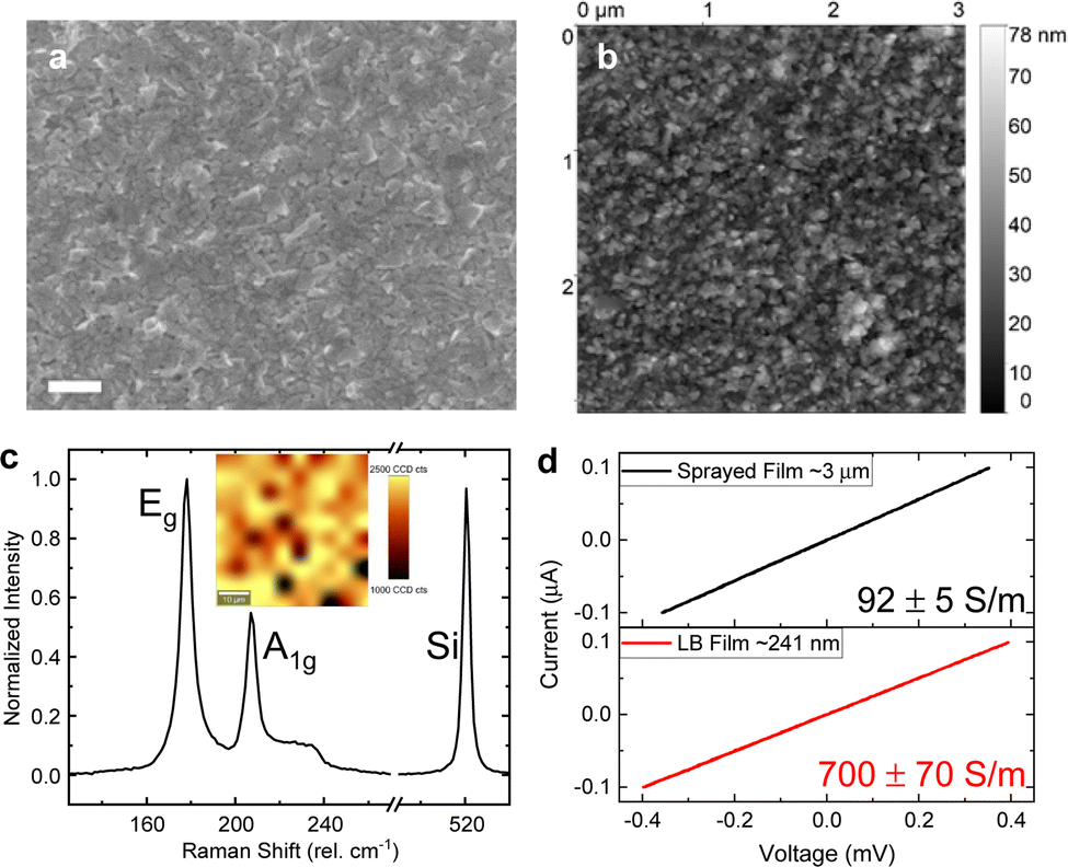 | ||
| Fig. 2 (a) SEM image (scale bar: 200 nm) showing good nanosheet alignment and (b) AFM image of the LPE-PtSe2 LB film. (c) Averaged Raman spectrum of the LPE-PtSe2 LB film. Inset: scanning Raman map of the Eg peak sum over a 50 by 50 μm2 area. (d) Current–voltage characteristics of conventional spray-deposited and LPE-LB deposited films, resulting in film conductivities of 92 ± 5 and 700 ± 70 S m−1, respectively. Note that the film thickness of the LB film (∼240 nm) is more than 12-fold thinner compared to the sprayed network (∼3 μm). | ||
An averaged Raman spectrum from 100 positions on a sample is shown in Fig. 2c. Two prominent peaks can be identified at 178 and 207 cm−1, which correspond to the in-plane Eg and out-of-plane A1g vibrational Raman active modes, respectively. The inset depicts the spatial distribution of the Eg mode at a location on the sample from which the averaged spectrum was measured. The Raman spectra contain well-defined, relatively narrow modes suggesting intact, crystalline nanosheets are deposited. Using our previously established quantitative metric for the estimation of PtSe2 nanosheet thickness from Raman spectroscopy,57 we estimate an average layer number of the nanosheets of 5.5. In previous work, we also established a correlation between the nanosheet layer number and lateral size,57,64 which allows us to infer the average lateral dimensions of the nanosheets as ∼60 nm (across the longest dimension) which is consistent with the microscopic characterization described above.
This modified LB film production method promises a higher conductive tiled network structure in comparison to randomly restacked porous nanosheet films produced by conventional spray deposition. To confirm this, another set of films were produced to allow for a direct comparison of LB-type and sprayed PtSe2 networks, respectively. Due to the relatively high mass required for spray deposition, a more polydisperse PtSe2 dispersion was used that was produced from centrifugation with a wider spread in the centrifugation boundaries (400g in the first step and 30000g in the second step). Note that this resulted in a more polydisperse size distribution and thicker, rougher films compared to the production method used for the remainder of the work (see the ESI†). Therefore, it was required to perform two subsequent deposition cycles in the case of this sample to yield a continuous network. While the more than 12 times thicker, ∼3 μm thick sprayed PtSe2 film (Fig. S2a, ESI†) showed a conductivity of 92 ± 5 S m−1, the ∼240 nm thick PtSe2-LB film (Fig. S2c, ESI†) showed approximately 7.6 times higher conductivity, 700 ± 70 S m−1 in 4-point probe measurements as shown in Fig. 2d. This is a result tentatively assigned to the better alignment of PtSe2 nanoflakes in the modified LB films. As a result, the modified LB film yields generally much thinner films with good conductivity. On the one hand, this reduces the material mass required for 2D material nanosheet network structures which is an important aspect for PtSe2 containing a precious metal. On the other hand, this can be beneficial for sensing applications due to better accessibility of the active material.
Fig. 3a depicts the current–voltage (Ids–Vds) curves measured on a sensor device where the film shown in Fig. 2a–c was contacted with interdigitated electrodes (inset) directly after fabrication and after 15 months. The slope of the curve yields a resistance of 61.8 kΩ for this device which corresponds to a conductivity of ∼1.95 S m−1 in this device structure. The lower conductivity of this 30 nm thin film compared to the 240 nm thick LB-type film (Fig. 2d) can be rationalized by a different nanosheet size distribution and hence different junction resistance, as well as a different device structure. The high resistance indicates lower conductivity than PtSe2 films grown by chemical vapour deposition11,65–67 which may be attributed to flake-to-flake junctions hampering charge carrier transport.52,68,69
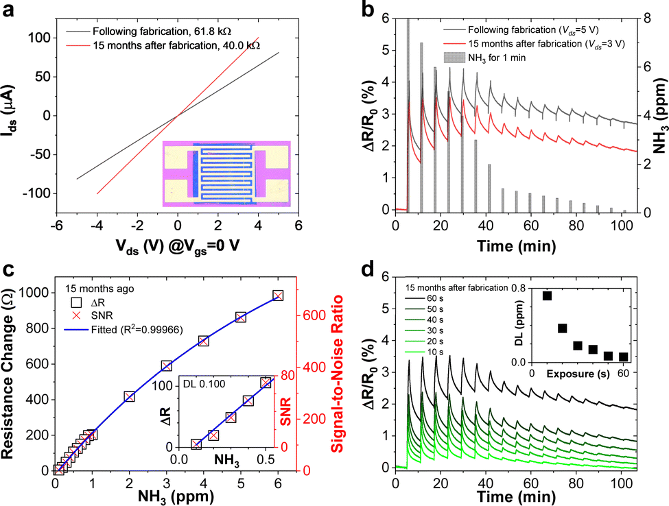 | ||
| Fig. 3 (a) Current–voltage (Ids–Vds) characteristics of an LPE-PtSe2 LB film sensor showing a noticeable conductance change after long-term exposure to the atmosphere. Inset: photograph of an LPE-PtSe2 LB film (blue area) underneath interdigitated electrodes. (b) Sensor response curves of the LPE-PtSe2 LB film sensor upon introduction of periodically decreasing concentrations of NH3 from 8 down to 0.1 ppm (gray columns) at room temperature. A NH3 sensor response is still observed 15 months later. (c) Resistance (open boxes) and SNR (red x-crosses) changes are proportional to the introduced gas concentration. Inset: zoomed-in plot in the lower NH3 concentration range. (d) Sensor response curves for 10 to 60 seconds of NH3 gas introduction (from light green to dark green). Inset: detectable NH3 gas concentration inversely decreases as the gas exposure time increases. | ||
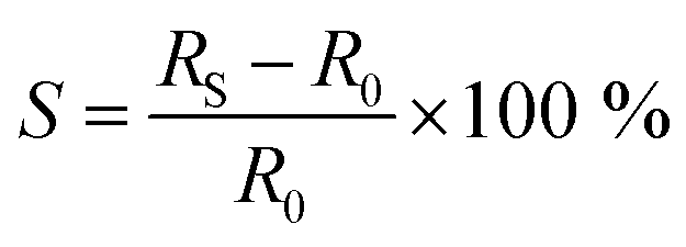
The contacted films were tested as ammonia sensors immediately after preparation and 15 months later to test the long-term stability of the device. Since many 2D materials, including group VI transition metal dichalcogenides,70 are prone to degradation, for example by exposure to ambient conditions, we placed particular emphasis on the long-term stability of the sensor, as nanosheet degradation can cause inferior device performance. The device was tested as a gas sensor by exposing it to various concentrations of NH3 in N2 (0.1 to 0.8 ppm). The analyte was periodically introduced for 1 minute at a fixed concentration and at room temperature, followed by introduction of dry N2 for 5 minutes for sensor recovery. No further treatments to enhance the recovery speed, e.g., ultraviolet light illumination or annealing at higher temperatures, were applied. At 5 V of bias voltage, real-time current changes of the structured LPE-PtSe2 LB film sensor can be calculated,
where RBase is the baseline of the initial sensor resistance, and N is the number of data points. The signal-to-noise ratios (SNRs) derived from the resistance increments at various NH3 concentrations are proportional to the gas concentration which is well-fitted to an exponential decay curve as shown in Fig. 3c. To be a true signal, the SNR must be at least three times larger or more according to the International Union of Pure and Applied Chemistry (IUPAC) definition.72 In our measurements, an SNR of 3.4 was obtained for a concentration of 0.1 ppm of NH3, setting a detection limit for this gas with LPE-PtSe2 LB film sensors. In the SNR changes depicted at various concentrations (Fig. 3c), one can determine a theoretical detection limit (DL) by extrapolation to the point where the SNR drops below 3. This theoretical DL reaches a value of only 0.059 ppm, which is remarkable, as detection of low concentrations of NH3 is challenging in chemiresistors because little charge is transferred compared to other analytes. This DL is one of the lowest values reported for LPE derived 2D material based gas sensors.14,73,74

The long-term stability of 2D material based devices under ambient conditions has often been a point of debate. Grown PtSe2 films are known to be stable under ambient conditions, however exfoliated films have never been investigated. Thus, we compare the performance of a sensor after it has been in N2 flow storage for 15 months. The film conductance surprisingly increased slightly as shown in Fig. 3a. The improved conductivity after 15 months of storage could be due to the formation of better intersheet contacts or residual water in the film acting as a p-dopant increasing the concentration of majority charge carriers. During NH3 gas sensing, interestingly, the peak-to-peak value of relative resistance changes slightly as the initial resistance decreased after 15 months, but the device exhibits higher SNR values because the RMS noise decreased. Fig. 3d presents the sensor response upon decreasing the NH3 introduction time from 60 to 10 seconds in the same period, indicating that the estimated detection limit exponentially increases from 0.059 to 0.721 ppm (inset).
In conclusion, the devices still function as a very sensitive ammonia sensor after 15 months of storage. This is a remarkable finding as the long-term stability of LPE derived devices has always been a point of discussion while the high stability PtSe2 has been so far only reported for thermally-assisted conversion (TAC) derived films.11
Conclusions
The formation of LB-type films into tiled networks from LPE-PtSe2 dispersions was achieved for the first time. This combination resembles a cornerstone for a high yield, scalable, low cost production of sensors. This method is suitable for highly sought after flexible and wearable devices. We characterized the tiled network films structurally and revealed homogeneous films with little roughness indicating good alignment of the PtSe2 flakes. We showed ∼7.6 times higher conductivity in the tiled nanosheet network films through the modified LB production method in comparison to the conventional spray-deposited films. Thus, this method allows deposition to much thinner conducting networks forming 2D materials. The sensor performance of the LPE-PtSe2 LB films showed high sensitivity toward NH3 down to 0.100 ppm, which is remarkably low compared to those of most other 2D material based gas sensors. Furthermore, we demonstrated the long-term stability of the PtSe2 based sensor over more than one year.Author contributions
K. L.: data curation, formal analysis, investigation, validation, visualization, writing – original draft, and writing – review & editing; B. M. S.: conceptualization, data curation, investigation, methodology, and writing – original draft; O. H.: formal analysis, investigation, and visualization; K. S.: data curation, formal analysis, and investigation, B. T.: investigation; T. H.: investigation; T. T.: investigation, methodology, visualization, and writing – review & editing; C. P. G.: formal analysis and investigation; J. N. C.: funding acquisition, and resources; Z. S.: funding acquisition and resources; M. S.: conceptualization, funding acquisition, methodology, supervision, and writing – review & editing; C. B.: conceptualization, funding acquisition, methodology, resources, visualization, supervision, and writing – review & editing; G. S. D.: funding acquisition, project administration, supervision, and writing – review & editing.Conflicts of interest
There are no conflicts to declare.Acknowledgements
This project has received funding from the European Union's Horizon 2020 research an innovation program under grand agreement no. 881603 (Graphene Flagship Core 3). We acknowledge the German Federal Ministry for Education and Research (BMBF) under the project no 16ES1121 (NobleNEMS). We thank the DTEC project Vital Sense and the University of the Bundewehr Munich for support. Z. Sofer acknowledges the Czech Science Foundation (GACR No. 20-16124J). M. Spasenović acknowledges funding from the Science Fund of the Republic of Serbia through the PROMIS funding scheme, project Gramulsen (number 6057070) and by the Ministry of Education, Science, and Technological Development of the Republic of Serbia (Ministarstvo Prosvete, Nauke i Tehnološkog Razvoja) under grant number 451-03-68/2022-14/200026.Notes and references
- A. K. Geim and K. S. S. Novoselov, Nat. Mater., 2007, 6, 183–191 CrossRef CAS PubMed.
- H. Schmidt, F. Giustiniano and G. Eda, Chem. Soc. Rev., 2015, 44, 7715–7736 RSC.
- C. Backes, A. M. Abdelkader, C. Alonso, A. Andrieux-Ledier, R. Arenal, J. Azpeitia, N. Balakrishnan, L. Banszerus, J. Barjon, R. Bartali, S. Bellani, C. Berger, R. Berger, M. M. B. Ortega, C. Bernard, P. H. Beton, A. Beyer, A. Bianco, P. Bøggild, F. Bonaccorso, G. B. Barin, C. Botas, R. A. Bueno, D. Carriazo, A. Castellanos-Gomez, M. Christian, A. Ciesielski, T. Ciuk, M. T. Cole, J. Coleman, C. Coletti, L. Crema, H. Cun, D. Dasler, D. De Fazio, N. Díez, S. Drieschner, G. S. Duesberg, R. Fasel, X. Feng, A. Fina, S. Forti, C. Galiotis, G. Garberoglio, J. M. García, J. A. Garrido, M. Gibertini, A. Gölzhäuser, J. Gómez, T. Greber, F. Hauke, A. Hemmi, I. Hernandez-Rodriguez, A. Hirsch, S. A. Hodge, Y. Huttel, P. U. Jepsen, I. Jimenez, U. Kaiser, T. Kaplas, H. Kim, A. Kis, K. Papagelis, K. Kostarelos, A. Krajewska, K. Lee, C. Li, H. Lipsanen, A. Liscio, M. R. Lohe, A. Loiseau, L. Lombardi, M. Francisca López, O. Martin, C. Martín, L. Martínez, J. A. Martin-Gago, J. Ignacio Martínez, N. Marzari, Á. Mayoral, J. McManus, M. Melucci, J. Méndez, C. Merino, P. Merino, A. P. Meyer, E. Miniussi, V. Miseikis, N. Mishra, V. Morandi, C. Munuera, R. Muñoz, H. Nolan, L. Ortolani, A. K. Ott, I. Palacio, V. Palermo, J. Parthenios, I. Pasternak, A. Patane, M. Prato, H. Prevost, V. Prudkovskiy, N. Pugno, T. Rojo, A. Rossi, P. Ruffieux, P. Samorì, L. Schué, E. Setijadi, T. Seyller, G. Speranza, C. Stampfer, I. Stenger, W. Strupinski, Y. Svirko, S. Taioli, K. B. K. Teo, M. Testi, F. Tomarchio, M. Tortello, E. Treossi, A. Turchanin, E. Vazquez, E. Villaro, P. R. Whelan, Z. Xia, R. Yakimova, S. Yang, G. R. Yazdi, C. Yim, D. Yoon, X. Zhang, X. Zhuang, L. Colombo, A. C. Ferrari and M. Garcia-Hernandez, 2D Mater., 2020, 7, 022001 CrossRef CAS.
- F. Schedin, A. K. Geim, S. V. Morozov, E. W. Hill, P. Blake, M. I. Katsnelson and K. S. Novoselov, Nat. Mater., 2007, 6, 652–655 CrossRef CAS PubMed.
- H. Li, Z. Yin, Q. He, H. Li, X. Huang, G. Lu, D. W. H. Fam, A. I. Y. Tok, Q. Zhang and H. Zhang, Small, 2012, 8, 63–67 CrossRef CAS PubMed.
- D. J. Late, Y. K. Huang, B. Liu, J. Acharya, S. N. Shirodkar, J. Luo, A. Yan, D. Charles, U. V. Waghmare, V. P. Dravid and C. N. R. Rao, ACS Nano, 2013, 7, 4879–4891 CrossRef CAS PubMed.
- K. Lee, R. Gatensby, N. McEvoy, T. Hallam and G. S. Duesberg, Adv. Mater., 2013, 25, 6699–6702 CrossRef CAS PubMed.
- H. Fang, S. Chuang, T. C. Chang, K. Takei, T. Takahashi and A. Javey, Nano Lett., 2012, 12, 3788–3792 CrossRef CAS PubMed.
- M. O’Brien, K. Lee, R. Morrish, N. C. Berner, N. McEvoy, C. A. Wolden and G. S. Duesberg, Chem. Phys. Lett., 2014, 615, 6–10 CrossRef.
- D. J. Late, T. Doneux and M. Bougouma, Appl. Phys. Lett., 2014, 105, 233103 CrossRef.
- C. Yim, K. Lee, N. McEvoy, M. O’Brien, S. Riazimehr, N. C. Berner, C. P. Cullen, J. Kotakoski, J. C. Meyer, M. C. Lemme and G. S. Duesberg, ACS Nano, 2016, 10, 9550–9558 CrossRef CAS PubMed.
- L. Pi, L. Li, K. Liu, Q. Zhang, H. Li and T. Zhai, Adv. Funct. Mater., 2019, 1904932, 1904932 CrossRef.
- X. Chen, C. Liu and S. Mao, Nano-Micro Lett., 2020, 12, 95 CrossRef CAS PubMed.
- M. Sajjad, E. Montes, N. Singh and U. Schwingenschlögl, Adv. Mater. Interfaces, 2017, 4, 1600911 CrossRef.
- X. Chia, A. Adriano, P. Lazar, Z. Sofer, J. Luxa and M. Pumera, Adv. Funct. Mater., 2016, 26, 4306–4318 CrossRef CAS.
- N. Rohaizad, C. C. Mayorga-Martinez, Z. Sofer, R. D. Webster and M. Pumera, Appl. Mater. Today, 2020, 19, 100606 CrossRef.
- Y. Hernandez, V. Nicolosi, M. Lotya, F. M. Blighe, Z. Sun, S. De, I. T. McGovern, B. Holland, M. Byrne, Y. K. Gun’Ko, J. J. Boland, P. Niraj, G. Duesberg, S. Krishnamurthy, R. Goodhue, J. Hutchison, V. Scardaci, A. C. Ferrari and J. N. Coleman, Nat. Nanotechnol., 2008, 3, 563–568 CrossRef CAS PubMed.
- A. B. Bourlinos, V. Georgakilas, R. Zboril, T. A. Steriotis and A. K. Stubos, Small, 2009, 5, 1841–1845 CrossRef CAS PubMed.
- M. Lotya, Y. Hernandez, P. J. King, R. J. Smith, V. Nicolosi, L. S. Karlsson, F. M. Blighe, S. De, Z. Wang, I. T. McGovern, G. S. Duesberg and J. N. Coleman, J. Am. Chem. Soc., 2009, 131, 3611–3620 CrossRef CAS PubMed.
- Y. T. Liang and M. C. Hersam, J. Am. Chem. Soc., 2010, 132, 17661–17663 CrossRef CAS PubMed.
- K. R. Paton, E. Varrla, C. Backes, R. J. Smith, U. Khan, A. O’Neill, C. Boland, M. Lotya, O. M. Istrate, P. King, T. Higgins, S. Barwich, P. May, P. Puczkarski, I. Ahmed, M. Moebius, H. Pettersson, E. Long, J. Coelho, S. E. O’Brien, E. K. McGuire, B. M. Sanchez, G. S. Duesberg, N. McEvoy, T. J. Pennycook, C. Downing, A. Crossley, V. Nicolosi and J. N. Coleman, Nat. Mater., 2014, 13, 624–630 CrossRef CAS PubMed.
- T. J. Nacken, C. Damm, J. Walter, A. Rüger and W. Peukert, RSC Adv., 2015, 5, 57328–57338 RSC.
- C. Zhi, Y. Bando, C. Tang, H. Kuwahara and D. Golberg, Adv. Mater., 2009, 21, 2889–2893 CrossRef CAS.
- J. N. Coleman, M. Lotya, A. O’Neill, S. D. Bergin, P. J. King, U. Khan, K. Young, A. Gaucher, S. De, R. J. Smith, I. V. Shvets, S. K. Arora, G. Stanton, H.-Y. Kim, K. Lee, G. T. Kim, G. S. Duesberg, T. Hallam, J. J. Boland, J. J. Wang, J. F. Donegan, J. C. Grunlan, G. Moriarty, A. Shmeliov, R. J. Nicholls, J. M. Perkins, E. M. Grieveson, K. Theuwissen, D. W. McComb, P. D. Nellist and V. Nicolosi, Science, 2011, 331, 568–571 CrossRef CAS PubMed.
- P. Yasaei, B. Kumar, T. Foroozan, C. Wang, M. Asadi, D. Tuschel, J. E. Indacochea, R. F. Klie and A. Salehi-Khojin, Adv. Mater., 2015, 27, 1887–1892 CrossRef CAS PubMed.
- V. Sresht, A. A. H. Pádua and D. Blankschtein, ACS Nano, 2015, 9, 8255–8268 CrossRef CAS PubMed.
- J. Kang, J. D. Wood, S. A. Wells, J.-H. Lee, X. Liu, K.-S. Chen and M. C. Hersam, ACS Nano, 2015, 9, 3596–3604 CrossRef CAS PubMed.
- J. R. Brent, N. Savjani, E. A. Lewis, S. J. Haigh, D. J. Lewis and P. O’Brien, Chem. Commun., 2014, 50, 13338–13341 RSC.
- D. Hanlon, C. Backes, E. Doherty, C. S. Cucinotta, N. C. Berner, C. Boland, K. Lee, A. Harvey, P. Lynch, Z. Gholamvand, S. Zhang, K. Wang, G. Moynihan, A. Pokle, Q. M. Ramasse, N. McEvoy, W. J. Blau, J. Wang, G. Abellan, F. Hauke, A. Hirsch, S. Sanvito, D. D. O’Regan, G. S. Duesberg, V. Nicolosi and J. N. Coleman, Nat. Commun., 2015, 6, 8563 CrossRef CAS PubMed.
- C. Gibaja, D. Rodriguez-San-Miguel, P. Ares, J. Gómez-Herrero, M. Varela, R. Gillen, J. Maultzsch, F. Hauke, A. Hirsch, G. Abellán and F. Zamora, Angew. Chem., Int. Ed., 2016, 55, 14345–14349 CrossRef CAS PubMed.
- Y. Liu, R. Cheng, L. Liao, H. Zhou, J. Bai, G. Liu, L. Liu, Y. Huang and X. Duan, Nat. Commun., 2011, 2, 579 CrossRef PubMed.
- R. J. Smith, P. J. King, M. Lotya, C. Wirtz, U. Khan, S. De, A. O’Neill, G. S. Duesberg, J. C. Grunlan, G. Moriarty, J. Chen, J. Wang, A. I. Minett, V. Nicolosi and J. N. Coleman, Adv. Mater., 2011, 23, 3944–3948 CrossRef CAS PubMed.
- G. S. Bang, K. W. Nam, J. Y. Kim, J. Shin, J. W. Choi and S.-Y. Choi, ACS Appl. Mater. Interfaces, 2014, 6, 7084–7089 CrossRef CAS PubMed.
- E. Varrla, C. Backes, K. R. Paton, A. Harvey, Z. Gholamvand, J. McCauley and J. N. Coleman, Chem. Mater., 2015, 27, 1129–1139 CrossRef CAS.
- Y. Liu, X. Ji, J. Liu, W. W. L. Tong, D. Askhatova and J. Shi, Adv. Funct. Mater., 2017, 27, 1703261 CrossRef PubMed.
- J. Kang, V. K. Sangwan, J. D. Wood, X. Liu, I. Balla, D. Lam and M. C. Hersam, Nano Lett., 2016, 16, 7216–7223 CrossRef CAS PubMed.
- P. Schiettecatte, A. Rousaki, P. Vandenabeele, P. Geiregat and Z. Hens, Langmuir, 2020, 36, 15493–15500 CrossRef CAS PubMed.
- E. Petroni, E. Lago, S. Bellani, D. W. Boukhvalov, A. Politano, B. Gürbulak, S. Duman, M. Prato, S. Gentiluomo, R. Oropesa-Nuñez, J.-K. Panda, P. S. Toth, A. E. Del Rio Castillo, V. Pellegrini and F. Bonaccorso, Small, 2018, 14, 1800749 CrossRef PubMed.
- M. M. Y. A. Alsaif, S. Balendhran, M. R. Field, K. Latham, W. Wlodarski, J. Z. Ou and K. Kalantar-zadeh, Sens. Actuators, B, 2014, 192, 196–204 CrossRef CAS.
- D. Hanlon, C. Backes, T. M. Higgins, M. Hughes, A. O’Neill, P. King, N. McEvoy, G. S. Duesberg, B. Mendoza Sanchez, H. Pettersson, V. Nicolosi and J. N. Coleman, Chem. Mater., 2014, 26, 1751–1763 CrossRef CAS.
- Y. Wang, Y.-Z. Zhang, D. Dubbink and J. E. ten Elshof, Nano Energy, 2018, 49, 481–488 CrossRef CAS.
- J. A. Carrasco, A. Harvey, D. Hanlon, V. Lloret, D. McAteer, R. Sanchis-Gual, A. Hirsch, F. Hauke, G. Abellán, J. N. Coleman and E. Coronado, Chem. Commun., 2019, 55, 3315–3318 RSC.
- A. J. Molina-Mendoza, E. Giovanelli, W. S. Paz, M. A. Niño, J. O. Island, C. Evangeli, L. Aballe, M. Foerster, H. S. J. van der Zant, G. Rubio-Bollinger, N. Agraït, J. J. Palacios, E. M. Pérez and A. Castellanos-Gomez, Nat. Commun., 2017, 8, 14409 CrossRef CAS PubMed.
- Y. Niu, J. Villalva, R. Frisenda, G. Sanchez-Santolino, L. Ruiz-González, E. M. Pérez, M. García-Hernández, E. Burzurí and A. Castellanos-Gomez, 2D Mater., 2019, 6, 035023 CrossRef CAS.
- M. Naguib, O. Mashtalir, J. Carle, V. Presser, J. Lu, L. Hultman, Y. Gogotsi and M. W. Barsoum, ACS Nano, 2012, 6, 1322–1331 CrossRef CAS PubMed.
- R. Z. Lange, K. Synnatschke, H. Qi, N. Huber, G. Hofer, B. Liang, C. Huck, A. Pucci, U. Kaiser, C. Backes and A. D. Schlüter, Angew. Chem., Int. Ed., 2020, 59, 5683–5695 CrossRef CAS PubMed.
- A. Harvey, C. Backes, Z. Gholamvand, D. Hanlon, D. McAteer, H. C. Nerl, E. McGuire, A. Seral-Ascaso, Q. M. Ramasse, N. McEvoy, S. Winters, N. C. Berner, D. McCloskey, J. F. Donegan, G. S. Duesberg, V. Nicolosi and J. N. Coleman, Chem. Mater., 2015, 27, 3483–3493 CrossRef CAS.
- C. Backes, B. M. Szydłowska, A. Harvey, S. Yuan, V. Vega-Mayoral, B. R. Davies, P. L. Zhao, D. Hanlon, E. J. G. Santos, M. I. Katsnelson, W. J. Blau, C. Gadermaier and J. N. Coleman, ACS Nano, 2016, 10, 1589–1601 CrossRef CAS PubMed.
- B. M. Szydłowska, O. Hartwig, B. Tywoniuk, T. Hartman, T. Stimpel-Lindner, Z. Sofer, N. McEvoy, G. S. Duesberg and C. Backes, 2D Mater., 2020, 7, 045027 CrossRef.
- X. Li, G. Zhang, X. Bai, X. Sun, E. Wang and H. Dai, Nat. Nanotechnol., 2008, 3, 538–542 CrossRef CAS PubMed.
- L. J. Cote, F. Kim and J. Huang, J. Am. Chem. Soc., 2009, 131, 1043–1049 CrossRef CAS PubMed.
- H. Kim, C. Mattevi, H. J. Kim, A. Mittal, K. A. Mkhoyan, R. E. Riman and M. Chhowalla, Nanoscale, 2013, 5, 12365 RSC.
- T. Tomašević-Ilić, J. Pešić, I. Milošević, J. Vujin, A. Matković, M. Spasenović and R. Gajić, Opt. Quantum Electron., 2016, 48, 319 CrossRef.
- S. Andrić, M. Sarajlić, M. Frantlović, I. Jokić, D. Vasiljević-Radović and M. Spasenović, Chemosensors, 2021, 9, 342 CrossRef.
- P. Blake, P. D. Brimicombe, R. R. Nair, T. J. Booth, D. Jiang, F. Schedin, L. A. Ponomarenko, S. V. Morozov, H. F. Gleeson, E. W. Hill, A. K. Geim and K. S. Novoselov, Nano Lett., 2008, 8, 1704–1708 CrossRef PubMed.
- F. Torrisi, T. Hasan, W. Wu, Z. Sun, A. Lombardo, T. S. Kulmala, G.-W. Hsieh, S. Jung, F. Bonaccorso, P. J. Paul, D. Chu and A. C. Ferrari, ACS Nano, 2012, 6, 2992–3006 CrossRef CAS PubMed.
- T. Tomašević-Ilić, Đ. Jovanović, I. Popov, R. Fandan, J. Pedrós, M. Spasenović and R. Gajić, Appl. Surf. Sci., 2018, 458, 446–453 CrossRef.
- F. Reincke, S. G. Hickey, W. K. Kegel and D. Vanmaekelbergh, Angew. Chem., Int. Ed., 2004, 43, 458–462 CrossRef CAS PubMed.
- H. Duan, D. Wang, D. G. Kurth and H. Möhwald, Angew. Chem., Int. Ed., 2004, 43, 5639–5642 CrossRef CAS PubMed.
- A. G. Kelly, D. O’Suilleabhain, C. Gabbett and J. N. Coleman, Nat. Rev. Mater., 2021, 7(3), 217–234 CrossRef.
- J. Wu, H. Li, Z. Yin, H. Li, J. Liu, X. Cao, Q. Zhang and H. Zhang, Small, 2013, 9, 3314–3319 CAS.
- A. Matković, I. Milošević, M. Milićević, T. Tomašević-Ilić, J. Pešić, M. Musić, M. Spasenović, D. Jovanović, B. Vasić, C. Deeks, R. Panajotović, M. R. Belić and R. Gajić, 2D Mater., 2016, 3, 015002 CrossRef.
- Y.-J. Li, W.-J. Huang and S.-G. Sun, Angew. Chem., Int. Ed., 2006, 45, 2537–2539 CrossRef CAS PubMed.
- C. Backes, D. Campi, B. M. Szydlowska, K. Synnatschke, E. Ojala, F. Rashvand, A. Harvey, A. Griffin, Z. Sofer, N. Marzari, J. N. Coleman and D. D. O’Regan, ACS Nano, 2019, 13, 7050–7061 CrossRef CAS PubMed.
- Y. Zhao, J. Qiao, Z. Yu, P. Yu, K. Xu, S. P. Lau, W. Zhou, Z. Liu, X. Wang, W. Ji and Y. Chai, Adv. Mater., 2017, 29, 1604230 CrossRef PubMed.
- C. Yim, V. Passi, M. C. Lemme, G. S. Duesberg, C. Ó. Coileáin, E. Pallecchi, D. Fadil and N. McEvoy, npj 2D Mater. Appl., 2018, 2, 5 CrossRef.
- T. Das, E. Yang, J. E. Seo, J. H. Kim, E. Park, M. Kim, D. Seo, J. Y. Kwak and J. Chang, ACS Appl. Mater. Interfaces, 2021, 13(1), 1861–1871 CrossRef CAS PubMed.
- G. Eda and M. Chhowalla, Nano Lett., 2009, 9, 814–818 CrossRef CAS PubMed.
- Q. Zheng, W. H. Ip, X. Lin, N. Yousefi, K. K. Yeung, Z. Li and J. K. Kim, ACS Nano, 2011, 5, 6039–6051 CrossRef CAS PubMed.
- Q. Li, Q. Zhou, L. Shi, Q. Chen and J. Wang, J. Mater. Chem. A, 2019, 7, 4291–4312 RSC.
- J. Li, Y. Lu, Q. Ye, M. Cinke, J. Han and M. Meyyappan, Nano Lett., 2003, 3, 929–933 CrossRef CAS.
- L. A. Currie, Pure Appl. Chem., 1995, 67, 1699–1723 CrossRef CAS.
- O. Leenaerts, B. Partoens and F. Peeters, Phys. Rev. B: Condens. Matter Mater. Phys., 2008, 77, 125416 CrossRef.
- S. Zhao, J. Xue and W. Kang, Chem. Phys. Lett., 2014, 595–596, 35–42 CrossRef CAS.
Footnote |
| † Electronic supplementary information (ESI) available: Additional comparison of LB-type nanosheet networks. See DOI: https://doi.org/10.1039/d2tc03889g |
| This journal is © The Royal Society of Chemistry 2023 |