
 Open Access Article
 This Open Access Article is licensed under a Creative Commons Attribution-Non Commercial 3.0 Unported Licence
Review of photocathodes for electron beam sources in particle accelerators
Jana
Schaber
 *ab,
Rong
Xiang
a and
Nikolai
Gaponik
b
*ab,
Rong
Xiang
a and
Nikolai
Gaponik
b
aHelmholtz-Zentrum Dresden-Rossendorf, Bautzner Landstraße 400, 01328 Dresden, Saxony, Germany. E-mail: j.schaber@hzdr.de
bTechnische Universität Dresden, Helmholtzstr. 10, 01069 Dresden, Saxony, Germany
First published on 17th February 2023
Abstract
This paper compares different photocathodes that are applicable for electron injector systems and summarizes the development in cathode technology in the last years. The photocathode is one of the key components of the facilities that provides electrons for many research experiments. Typically, a high efficiency and a long operation time are desired, thus the photocathode needs to be robust against any rest gases occasionally available during operation. Low thermal emittance and fast response time are special requirements for the accelerator community. These parameters are commonly used to compare the various cathode materials. Metals and plasmon-enhanced materials emit electrons from the near surface, whereas semiconductors emit photoelectrons mostly from the bulk region. We compare metal photocathodes such as magnesium, copper and lead, with semiconductor photocathodes such as cesium telluride, antimonide photocathodes and III–V semiconductor photocathodes. GaAs and its typical application for the generation of spin-polarized electrons is discussed and special attention has been paid to the emerging GaN as a potential novel photocathode. The above mentioned state-of-the-art cathodes are compared regarding their preparation approaches, quantum efficiency, lifetime, response time and their status of application. This work is aimed to provide a guideline for particle accelerator researchers in their choice of the cathode material. Thermionic cathodes and field emission cathodes are not discussed in this review.
1 Introduction
Electron sources represent a key component in modern technologies such as microscopes,1–3 radio transmitters,4 and X-ray tubes for medical diagnostic devices.5 A wide range of applications is covered by the ability to accelerate electrons in a particle accelerator. The development of a better electron source is crucial for both fundamental and applied research. The improvement of the existing electron sources is directly linked to strong demands on higher electron currents, higher repetition rates or high brightness beams.6,7In the last decades, the development in accelerator technology contributed to advanced cancer diagnostic and therapy,8 and helped to understand chemical reaction mechanisms9 and molecular excitation and vibration states.10 Free electron laser (FEL), especially X-ray free electron laser (XFEL) facilities11,12 and terahertz (THz) radiation sources13 are powerful tools with a wide application in biomedicine, security imaging and condensed matter physics. These tools require high brightness electron beams that are generated from so-called photocathodes inside a photoinjector.
The principle of an accelerator electron source begins with the generation of electrons and the subsequent acceleration of those downstream. The electrons are accelerated away from the cathode by an electric field, and afterwards they are collimated to form a compact electron bunch. A vacuum environment protects the cathode from toxic contaminations and prevents electron scattering on gas molecules or residual particles.
In accordance to the nature of the electric field applied to the cathode, accelerator facilities can be distinguished into three different injector types.14–16 One possibility is to apply a direct current (DC) electric field between cathode and anode. Depending on the applied DC field, the electrons gain energies between 100–500 kV. A disadvantage of DC electron sources is that electrons are not accelerated to relativistic energies. Such DC electron sources are used in Cornell Laboratory for Accelerator-Based Science and Education (CLASSE),17 National Laboratory for High Energy Physics (KEK)18 and Microtron Accelerator Mainz (MAMI).19
Another possibility instead of a DC field is the application of a radio-frequency (RF) field. In RF injectors the cathode is surrounded by a special shaped resonance cavity. Thus, no anode is needed. Deutsches Synchrotron (DESY),20 European Organization for Nuclear Research (CERN)21 and Paul-Scheerer Institute (PSI)22 use such RF injector systems.
A special type of RF technology is used in the superconductive radio-frequency (SRF) injector. It also has a resonance cavity, made of niobium (Nb) which allows a superconducting state at very low temperatures. Therefore, the Nb cavity has to be cooled constantly at a cryogenic temperature to guarantee this superconductivity. SRF injectors are used for example at ELBE23 and at Brookhaven National Lab (BNL).24
As mentioned, the cathode is the origin of the generated electrons and can be a metal, including plasmon-enhanced materials, or a semiconductor. An energy source is necessary to excite electrons above the work function with the desired consequence of the emission of cathodic electrons. The necessary energy can be supplied either thermally, with an electric field or with photons. The thermionic and the field emission are the mature methods and work robustly. However, the photoemission offers more advantages, for example that the electron bunches can be time structured.
The choice of suitable cathodes for high brightness electron beams depends on many factors. A perfect photocathode should provide a high quantum efficiency (QE) at convenient laser wavelength, long lifetime, fast response time and low thermal emittance. Especially, the criterion of high QE has an extraordinary importance and can not be fulfilled by the existing photocathodes.25 For example, none of these known cathodes can provide such high QE to meet a high beam current as it is required for future energy recovery lines (ERL) applications.26–28
The development of better photocathodes is progressing steadily and rapidly. Metal cathodes such as copper (Cu), magnesium (Mg) and lead (Pb) are used as the first cathodes when an accelerator facility is commissioned. But the fast development of the particle accelerator devices and the strong desire to achieve higher bunch charges and currents leads to the usage of semiconductor photocathodes such as cesium telluride (Cs2Te), alkali antimonide (K2CsSb) or gallium arsenide (GaAs). In the last decades, an intensive research on GaAs led into the field of III–V semiconductors and especially gallium nitride (GaN) was identified to be a promising photocathode for future high current applications in the particle accelerator field.
In SRF Guns the right choice of the photocathode is extremely relevant, because the cavity is sensitive to any contamination. This risk is the potential release of the photocathode components into the cavity and its re-deposition at high field regions. Furthermore, the prevention of a potential overheating of the photocathode is the next considerable point. A proper thermal contact is crucial to avoid a cathode overheating, that is caused by laser irradiation and RF dissipation. One possibility for the heat dissipation is to conduct it into a liquid helium environment of the cavity. Another possibility represents the non-contact cathode, which requires an external cooling. In the non-contact mode, the biggest advantage is that the cathode can be operated at temperatures different from the cavity temperature.29
In this review, we introduce the requirements for high current electron beams and discuss different photocathodes regarding to their quality and performance. We compare metal photocathodes with semiconductor photocathodes and give an outlook on the potential use of III–V semiconductors, especially GaN as a considerable photocathode.
2 Requirements for high current electron beams
In the following section the requirements for high current electron beams and fundamental key terms are described. Fulfilling the desired requirements such as QE, long lifetime, low dark current, low thermal emittance and fast response time lead to the promising developments in the field of semiconductor photocathodes.25,30,312.1 Quantum efficiency (QE)
QE is one of the most important parameters, when dealing with photocathodes. QE is defined by the ratio of the number of generated photoelectrons divided by the number of incident photons,7 as shown in eqn (1). The QE can be more practically calculated by the ratio of h (Planck constant), c (speed of light) and I (measured photocurrent from the photocathode) to qe (elementary charge of an electron), λ (incident wavelength) and Plight (power of incident light), also shown in eqn (1).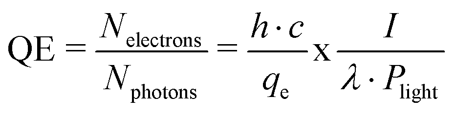 | (1) |
Therefore, a maximum QE is achieved by a minimum laser power and a maximum photocurrent.
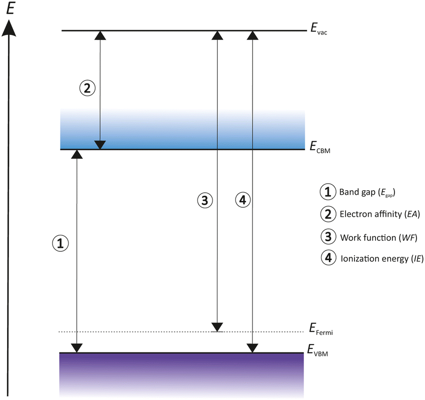
The electronic structure of an emissive material and its relation to the outside environment are characterized by many key terms. An overview of these key terms such as work function, electron affinity and Fermi level (EFermi) has been summarized in Fig. 1 to convey the basic principles of a photocathode.32
 | ||
| Fig. 1 Schematic representation of the fundamental key terms in photoemission processes. | ||
The electronic structure of the material surface differs from sample to sample, caused by many internal and external factors such as lattice structure, material defects, morphology and surface composition, especially its surface cleanness. As shown in Fig. 1, the energy levels of electron transport are defined as conduction band (CB) and valence band (VB). The conduction band minimum (CBM) represents the lowest energy level of the unoccupied state of the uncorrelated electron and quasi-electrons. In contrast the valence band maximum (VBM) is the highest energy level of occupied states with correlated electrons. The energy difference between these two levels is called band gap (Egap). The EFermi is the highest occupied level where electrons are flexible and can move around freely. Therefore, EFermi marks the boundary between occupied and unoccupied states in a continuum of states.
A vacuum energy barrier (Evac) prevents flexible electrons from escaping from the materials surface. Thus, Evac defines the potential energy of an electron positioned in a space outside of the solid. The Evac location is strongly influenced by the nature of the material surface.
The energy difference between Evac and VBM is defined as ionization energy (IE) and characterizes the minimum energy needed to remove an electron out of the material. Whereas the electron affinity (EA) is the energy difference from Evac to CBM.
The work function (WF) is the necessary energy to remove an unbounded electron from EFermi and place it outside of the surface in free space.
For semiconductors the work function depends on EFermi, influenced by the density of states, temperature and carrier concentration. The work function prevents a free electron at EFermi to escape from the solid into the outside space, and the work function is influenced by two main components, namely a bulk component (electronic density of states in the solid) and a surface component (redistribution of charges at the surface). A redistribution of the electron density can occur which is a consequence of coulomb repulsion and Pauli exclusion from adsorbates on the surface. Any deposition of an electronegative adsorbate on the surface results in an electron transfer that increases a surface dipole and influences the related surface terms.
2.2 Thermal emittance and mean transverse energy (MTE)
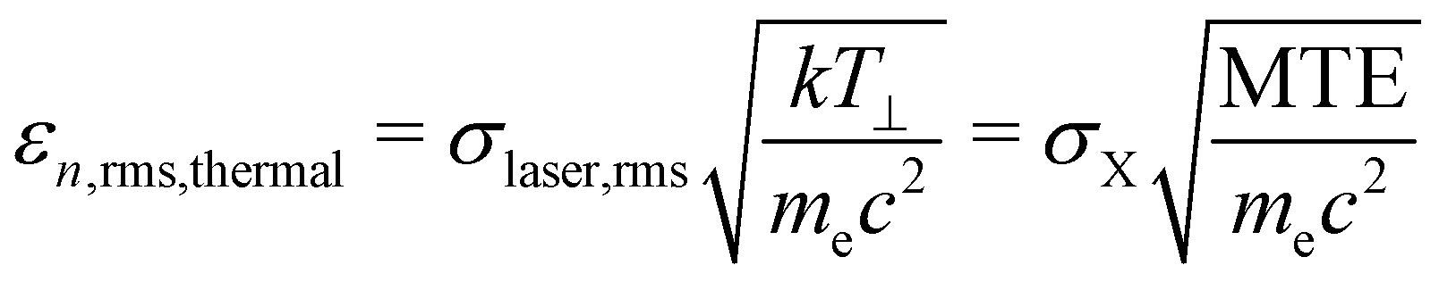
Thermal emittance is an important key factor for the maximum achievable electron brightness, depending on the electron source. Thermal or intrinsic emittance describes the transverse momentum of emitted electrons from the material surface. It considers the cathode material, its surface quality (roughness and crystallinity), the applied electric field and the incident laser wavelength.33 Therefore, thermal emittance includes all the physics in the emission process and the cathode material properties and summarizes the divergence of the cathode emittance.25 The thermal emittance also depends on the Mean Transverse Energy (MTE) of electrons. MTE does not depend on the spot size of the drive laser, but reflects the properties of the cathode material, the cathode surface condition34–36 and the drive photon energy.37 Thus, MTE is also an important parameter for describing the cathode properties. The electric field on the surface, the crystal defects inside the semiconductor cathode,38 and the operation temperature25 have an influence on the MTE as well.Eqn (2) shows a widely used formula to describe the thermal emittance.7 Often different formulas are given considering even more emission parameters such as Egap, electron affinity or photon energy.
 | (2) |
σ laser,rms is the root mean square (rms) spot size of the laser and c the speed of light in vacuum. kT⊥ means the electrons effective transverse energy, me the electron mass and σX, and MTE are the rms size of the electron bunch, starting from the cathode, and the mean transverse energy of the electron beam, respectively. kT⊥ will approach the crystal lattice temperature when the photocathode is illuminated with a photon energy near its Egap. For GaAs, as a negative electron affinity (NEA) photocathode, kT⊥ is 25 meV at room temperature. If the wavelength is greater than the Egap, the effective temperature of the electrons increases. For non NEA cathodes the effective temperature is always above the cathodes temperature.25
In fact, for photocathodes a low thermal emittance is desirable and typical values are between 0.5–1.5 μm, depending on the cathode material.
2.3 Lifetime
The photocathodes lifetime and its performance are determined by many factors, but especially by the vacuum conditions. All of the known photocathodes require an ultra-high vacuum (UHV) environment to provide a sufficient QE and lifetime. Photocathodes are influenced immediately by any residual gases inside the UHV system. Surface poisoning and the related efficiency loss were studied and reported for metal cathodes exposed to gases for longer time.39 However, for metal photocathodes the adsorption of residual gases is typically less significant than for semiconductors. Semiconductors such as Cs2Te or GaAs are immediately influenced by any vacuum instabilities.40,41 The photocathode surface is contaminated by the adsorption of residual gas or molecules, leading to the increase of the electron affinity and obstructing the ejection of photoelectrons into the vacuum. The photoemissive cathode might also react with the residual gas molecule, leading to a band structure change. Therefore, it is necessary to keep the pressure as low as possible with the help of suitable vacuum pumps for UHV application (ion pumps and non-evaporable getter (NEG) pumps). The combination of these pumps can guarantee a vacuum between 10−10–10−11 mbar. Especially GaAs is highly sensitive to any residual gases and requires minimum 10−11 mbar or better vacuum.2.4 Dark current
Dark current means the unwanted electron emission in photoinjector systems.42,43 The main sources for field emission are the photocathode itself and/or the cavity behind the photocathode. Undesired electrons are hazardous to the components downstream and have to be sorted out. It is crucial to discover the source location in order to prevent possible damage on the accelerator components.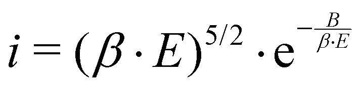 | (3) |
The undesired field emission is characterized by the Fowler–Nordheim relation to describe the current density,42,44 shown in eqn (3). E is the electric field, B is a material depended parameter and β is the field enhancement factor, depending on the emitters geometry. This relation fits best to metallic emitters but can be applied also to semiconductor materials. The sources for dark current are usually irregularities on the photocathode surface which appear as macroscopic tips, needles or particles. Exposed to the electric field, these surface irregularities cause a high β.43,45 Thus, it is necessary to provide a smooth and particle-free surface before an RF field is applied to the cathode.
Scanning electron microscopic (SEM) and atomic force microscopy (AFM) are useful tools to characterize the surface structure and the roughness. Both techniques are widely used and detectable breakdown spots in the cathode surface are identified as a reason for the strong emission.43 Small irregularities in the grain boundaries and defects in the crystal structure are also assumed to cause strong emission. The best way to minimize surface irregularities is to use a polished mirror-like materials of high-crystal quality.44
2.5 Response time
An important parameter for the generation of short electron pulses in less than picosecond (ps) regime is response time.7Response time means the total time elapsed between the excitation of the electrons by incident photons, their tunneling towards the surface and their final escape from the cathode surface into the vacuum.25 Photosensitive materials with a longer response time are not considered to be a photocathode in particle accelerators because of their temporal spread. Thus, a complex bunching and chopping downstream of the electron beam path would be necessary. Recent measurements of Cs2Te, tri-cesioantimony (Cs3Sb) and GaN photocathodes show prompt response in femtosecond (fs) regime. Response time can be diagnosed with a deflecting cavity synchronized to a laser pulse train.30,46,47
2.6 Survivability in RF field
The successful operation of a photocathode in accelerator RF injectors is determined by their survivability. Many photocathodes, metallic or semiconductor materials, were tested as electron sources in accelerator injectors. Bi-alkali photocathodes such as Cs2Te and K2CsSb survive several months in operation, independent on DC or RF injector.48,49Contrary, the successful operation in SRF injectors is more challenging than in DC or RF injectors. The operation of photocathodes based on cesium (Cs) and its compounds is quite difficult compared to bulk metal cathodes. One of the most common challenges is the possible vaporization of cathode components into the cavity system, causing photocathode degradation. There is a strong need to maintain the cathode at a suitable temperature inside of the cryogenic SRF environment. For example, the overheated Cs2Te in ELBE resulted in such a contamination of the cavity.23,50
Furthermore, the possibility of field emission at high fields and multi-pacting at low fields should be taken into account. It is important to note that a successful example for a long survivability of a bi-alkali (K2CsSb) photocathode can be given.51
2.7 Electrical conductivity
The electrical conductivity plays a decisive role when dealing with photocathodes because electrons are permanently released from the material surface. As a logical consequence, the surface of the material remains ionized until the material can draw electrons via the contact to the cathode body and neutralize the caused ionization. If the photocathode is not able to track new electrons via the contact over the cathode body, the surface remains ionized. Thus, the photocathode is going to run out of its electrons and consequently, the cathode will lose QE.Pure semiconductors are much less conducting than metals because the electrical conductivity of semiconductors depends on many factors such as temperature, pressure, and the concentration of supplied impurities.5 Through the implantation of impurities, so called dopants, into the intrinsic semiconductor crystal lattice, the conductivity can be increased and varied. Dopant atoms replace the native host atoms in its intrinsic crystal lattice. Ideally, dopant atoms should have the same size as the host atoms, meaning the selection of a dopant nearby the position of the intrinsic semiconductor host atom in the periodic table of elements. The dopant atom has one greater or one fewer electron in the valence shell than the host atom.
3 Photoemission models: one step and three-step model
Two approaches are commonly used to describe the photoemission process, namely, the one-step model52 and the three-step model, both summarized in Fig. 2. | ||
| Fig. 2 Comparative illustration of (a) the one-step model and (b) the three-step model. | ||
The one-step model uses an approximation where electrons are excited from a bound state to a free state out of the material. The model assumes a well-defined crystalline state and is often used to study the band structure. For many photoemissive materials the one-step model is not practical as it does not take electron scattering effects into account.
The three-step photoemission model was developed by Berglund and Spicer53 and is shown in Fig. 2 on the right side. As the name suggests, the photoemission process of this model is explained in three steps, consisting of the optical excitation, the transportation of the electron towards the surface and its escape into the vacuum. The three steps are treated independently and separately from each other.
The first of three steps is the excitation from VB to CB. The electrons of the VB absorb the energy of the incident photons and are injected into the CB. This step happens only if the incident photons have enough energy to lift the electrons over the Egap barrier.
The second step describes the scattering events. The photoelectrons in the CB move to the cathode surface via diffusion or drifting. During this process the electrons lose a part of their energy due to scattering or recombination with other atoms. This step enlarges the energy spread of photoelectrons.
The last step represents the release of the photoelectrons into the vacuum. The photoelectrons reach the surface and have to pass the Evac barrier in order to escape into the vacuum. To make it easier for the photoelectrons, it is advantageous to reduce Evac as much as possible, for example with the deposition of a thin film of a low work-function material, such as alkali–metals. As a consequence, the Evac is close to the energy of the CB or situates below the CBM. This state is called a negative electron affinity (NEA) surface.
Considering metal photocathodes with no band structure, incident photons are absorbed and electrons are moving towards to the surface in order to escape into the vacuum. With a high probability of scattering events with other electrons, most of the traveling electrons lose nearly all of their energy in the way that they are no longer able to escape the cathode surface. Only electrons within one electron mean free path are able to escape the surface. Therefore, metal photocathodes have a generally low QE.
Semiconductors show a much higher QE compared to metal photocathodes. Incident photons with an energy higher than the Egap, excite electrons from the VB into the CB. Once the photoelectrons enter the CB, almost no scattering from electron–electron collision can occur. Thus the electron mean free path of photoelectrons in semiconductors is much longer than in metals. Consequently, more photoelectrons are able to escape the surface and contribute to the QE. Scattering processes in grain boundary or lattice scattering still occur, but the photoelectrons loose only a small part of their energy.5
These two important and widely used models of the photoemission process can be further extended with the help of simulation methods such as Monte-Carlo,54–57 density functional theory (DFT)58–62 and machine learning.63–68 DFT, for example, is used to calculate energy states based on electron densities and their energies. The calculations show different scenarios of covalent binding interactions between different atoms and the resulting work functions.69 Thus, the formation of a dipole Ga–O–Cs layer in a Cs and oxygen (O2) activated GaN and GaAs can be assumed.23,51 The DFT calculations support experimental results well and can explain why the assumed formation of Ga–O–Cs on the surface plays an important role in achieving NEA surfaces. Due to this dipole layer sequence, researchers like Machuca70 and Wu71 tried to apply O2 first in the preparation process. The goal was to form a more stable Ga–Ox foundation before Cs is applied to the semiconductor surface with the aim to achieve a higher QE.
4 Metal photocathodes
In the following sections the most common materials for photoinjectors are presented. The materials are described and summarized regarding their preparation method and their quality such as QE, lifetime, response time and thermal emittance. References are taken from international labs such as DESY, CERN, BNL, Jefferson Lab (JLAB), Italian Institute for Nuclear Physics (INFN), KEK and ELBE.We compare metal photocathodes (section 4) possessing low QE with semiconductor photocathodes (section 5) possessing high QE.
Pure metal photocathodes such as Cu, Mg or Pb have a high work function and require ultra-violet (UV) light, which is the biggest disadvantage for high average current applications. However, metal photocathodes have also some advantages. The biggest advantage is their high robustness, so that they can survive years in operation.33,50 Mg has a relatively low work function (3.6 eV) compared to Cu (4.6 eV) or Pb (4.3 eV). Mg can provide a QE of about 0.2% when illuminated with 258 nm UV light after a proper cleaning process.29 Another advantage is that the preparation of such metal photocathodes is less complex compared to the preparation of semiconductor photocathodes, which is further described in the following sections.
4.1 Preparation
The most commonly used cleaning method is the thermal cleaning in vacuum environment. Once the cathode is installed in a UHV chamber, it undergoes a thermal cleaning at a certain temperature with the aim to desorb adsorbates such as water (H2O), hydrogen (H2), carbon monoxide (CO) and carbon dioxide (CO2) from its surface. The typical thermal cleaning temperature can be varied between 200–300 °C and is applied for several hours or is even kept up to one day. Beside the thermal cleaning in vacuum, UV ozone (O3) laser cleaning, hydrogen (H+) or argon ion (Ar+) sputter-cleaning should be considered as well.39,50,72An UV laser cleaning represents a suitable method and is used for the surface cleaning of a Mg cathode in ELBE. The Mg cathode consist of a 10 mm, high purity (99.999%) plug and undergoes an UV laser cleaning with 258 nm, 100 kHz repetition rate and 100 mW laser power. The area cleaned by UV light is seen as a 4 mm bluish spot in the middle of the 10 mm original Mg plug, shown in Fig. 3. This cleaning process is repeatable and thus the cathode can be reused several times.29 Even when the cathode is exposed to poisonous gases, the UV laser cleaning can be used to remove adsorbed gases from the surface and to create a clean Mg surface once again.
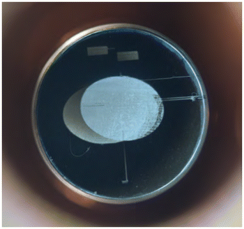 | ||
| Fig. 3 Photograph of a 10 mm Mg cathode inside the UHV chamber. The middle bluish part of a spot size of 4 mm was cleaned with an UV laser. | ||
Metal cathodes are mostly treated with a soft chemical cleaning and undergo a surface polishing till a polished mirror-like surface is achieved. The mirror-like metal cathode is stored under protection gas atmosphere until it is installed in the UHV chamber.
Other metal photocathodes such as Cu73 or Pb,74 used in BNL and DESY, are prepared in the same way as Mg cathodes.
4.2 Quantum efficiency and lifetime
Metal cathodes show relatively low QE values in the range of 10−4 to 10−1 compared to semiconductor photocathodes.33 As mentioned in Section 3, this is caused by the energy loss due to scattering events and only electrons with one electron free mean path are able to enter into the vacuum.It is well known that the photoemission process in metals takes place in the first surface layers75,76 and therefore strongly depends on the surface quality. To be briefly exposed to air is less hazardous for metal photocathodes than for cesiated photocathodes.29 Thus, the QE of the metal cathode drops less by a short exposure. Of course, the exposition to gases for longer time causes oxidation and leads to a change of the surface work function.
4.3 Thermal emittance
The thermal emittance is strongly influenced by the photocathode surface roughness and its morphology. The average roughness has to be as low as possible to reduce the probability of unwanted emittance. A commonly and widely used practice is the usage of a cathode with a diamond-turned surface, having an average roughness of less than 5 nm.73 The values for the divergence of the electron beam, caused by the emission of metal cathodes are about 0.41 ± 0.03 mm mrad−1.77 For the thermal emittance of Mg photocathodes multiple publications showed a low value with an upper limit of 0.5 mm mrad mm−1, driven with 4.66 eV in the warm RF gun.78,79 Thus, Mg is a good candidate for high brightness photocathodes.The application of an electric field can be beneficial to reduce the work function and consequently to increase the QE. This effect is called Schottky effect.7 The original work function including the Schottky effect is combined into a new term, the effective work function.
Michaelson80 showed that the work function not only depends on the surface quality and vacuum conditions, but also on the crystal orientation of the metal. Studies showed that the use of a single crystal benefits the photoemission to be more uniform compared to the photoemission of a polycrystal.81 Since then studies were carried out how the crystal orientation and its roughness influences the beam parameters, e.g. the mean transverse energy spread.82 However, it should be noted that inspite of the expected advantages of monocrystals, the polycrystalline cathodes are still widely used.29,83
The thermal emittance of a Cu photocathode was measured by H. Qian in a RF gun at 50 MV m−1 and showed 0.92 mm,79 when it was illuminated with a 266 nm UV laser.
4.4 Response time
The response time for Cu and Mg cathodes is less than picoseconds.7,84 Therefore, metal photocathodes are often used for accelerator applications where only low average current, and a fast response time is required.5To sum up, metal cathodes should be considered as robust photocathodes for any type of injector, providing an average electron beam with acceptable QE.
5 Semiconductor photocathodes
Semiconductor photocathodes are sub-divided into positive electron affinity cathodes (PEA) and negative electron affinity cathodes (NEA). The main difference between the two types is the location of the Evac, shown in Fig. 4. For PEA cathodes Evac is above the CBM and for NEA cathodes Evac is below the CBM.25 Cs2Te and alkali antimonide belong to PEA cathodes, whereas GaAs and GaN belong to NEA cathodes.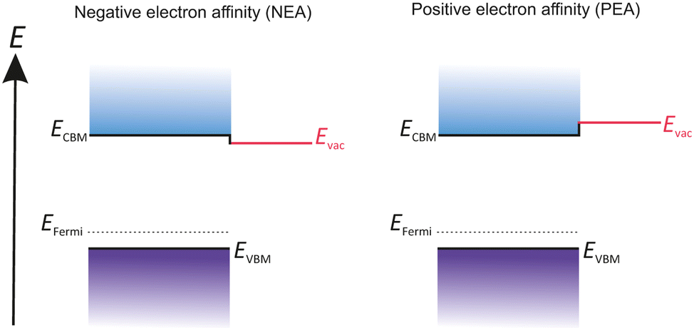 | ||
| Fig. 4 Comparative illustration of the difference between PEA and NEA surfaces regarding the location of the Evac. | ||
The semiconductor photocathodes for particle accelerators are further sub-divided according to their fabrication method: (i) crystals grown on a substrate or (ii) the deposition of Cs and O2 on an as-received semiconductor. Cs2Te and antimonide photocathodes belong to (i) and are typically grown on a substrate that has to be cleaned in advance before the crystal growth can be realized.
In contrast semiconductors such as GaAs and GaN are commercially available and only a deposition of Cs and an electronegative ingredient such as O2 are needed to obtain a photocathode. Therefore, these semiconductor photocathodes belong to (ii).
5.1 Cesium telluride
Alkali metals such as potassium (K), sodium (Na) and Cs have only one electron in the outer shell of their electron configuration. This single electron in the outer shell has a great affinity to form a new ionic bond with others. Tellurium (Te) has two single electrons in his 4p electron orbitals which react easily with alkali metals like Cs and form a stable compound material. One of the most used semiconductor compound materials as a photocathode in photoinjectors is Cs2Te, which provides a long operational lifetime and a high QE. | ||
| Fig. 5 Schematic overview of a typical layer sequence for a Cs2Te photocathode, based on the original approach taken from ref. 40. | ||
The initial conditions for this type of photocathodes are UHV and highest purity of evaporators. In this established process, Cu or molybdenum (Mo) can be used as a substrate, which should be mirror-like polished and cleaned with acetone and ethanol in advance. The mirror-like polished substrate is then installed in the UHV chamber and heated up to 500 °C for 30 min. This thermal cleaning aims to remove residual adsorbates like gases or particles from the substrate surface. After the substrate is outgassed, it is kept at 120 °C. On this hot substrate Te and Cs are deposited in sequence, meaning at first Te and afterwards Cs. During the Cs deposition the cathode is illuminated with UV light to detect the photocurrent simultaneously. The photocurrent increased depending on the deposited amount of Cs on the Te layer. The Cs deposition is finished when the photocurrent exceeds a maximum and starts to descend.
Besides this sequential deposition process, a co-evaporation of Cs and Te at the same time is optional.85 Both techniques deliver high quality and reproducible cathodes. The thickness is monitored by a quartz micro balance crystal during the manufacturing process.
The substrate has an high influence on the performance of the grown Cs2Te photocathode. It is well known that substrate atoms can diffuse into the deposited film or the substrate crystal structure does not match to the crystal structure of the photocathode. Thus, lattice mismatch happens. Furthermore, Cu atoms diffuse into Te and cause some island growth which leads to a lower QE compared to the Cs2Te cathode on a Mo substrate.40 Besides the standard substrates (Cu and Mo), Nb86 can be considered as a potential substrate for Cs2Te.
Fig. 6a shows an example of the main components of the preparation chamber at ELBE (left side), containing the Cs and Te evaporators from SAES and a mask between the cathode body and dispensers. The freshly prepared Cs2Te photocathode can be seen in Fig. 6b on the right side. The grown Cs2Te crystal is 4.0 mm in diameter on a Cu substrate and has a violet color, which appears orange due to light incidence in Fig. 6b.
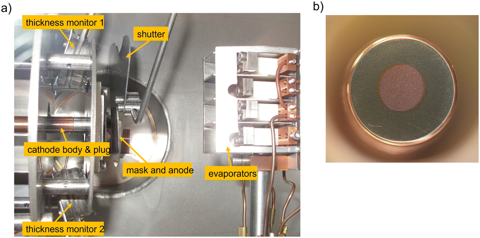 | ||
| Fig. 6 (a) The interior of the Cs2Te preparation chamber, showing a cathode body with a plug, shutter, a mask which is also an anode, two thickness monitors, and Cs and Te evaporators and (b) photo of a freshly deposited Cs2Te layer (4 mm in diameter) on a Cu plug. | ||
Especially the thickness of the deposited Cs2Te layer plays a superior role in the QE performance and is still under optimization at DESY and INFN.91,92
High QE of Cs2Te can be achieved only under an UV-excitation, which is the biggest disadvantage of this photocathode compared to the antimonide-based photocathodes that are operating under green light, as described in the next chapter. Another disadvantage is the high sensitivity to any residual CO2 or O2 molecules in the UHV system. The adsorption of gas molecules changes the surface work function negatively so that the QE drops. Further detailed information is given in Section 5.1.4.
Cs2Te has a MTE of 0.55 eV and a thermal emittance of 0.43 π mm mrad mm−1 from Floettmanns estimation.95 In ELBE SRF gun, the thermal emittance of an old Cs2Te cathode (QE was below 1% at 258 nm) was measured 0.6–0.7 mrad mm−1, and the average kinetic energy was about 0.35 eV.96 However, the thermal emittance of Cs2Te was measured by P. Huang and reached about 1.1 π mm mrad mm−1 in the warm RF gun at 40 MV m−1 and at 257 nm of the drive laser.97
In its own turn, CO, N2 and CH4 did not show any significant effect on the lifetime of the Cs2Te cathodes.40
Summarizing, Cs2Te is a good choice as it shows a reasonable QE, lifetime, fast response time and a good survivability under RF fields. The preparation is relatively simple and guarantees QE values between 10–20% under UV excitation. The main disadvantage, besides the requirement of intensive UV light, is its low robustness against vacuum instabilities, especially against O2 and CO2. The rejuvenation of the poisoned cathode is possible, but requires UV light and additional thermal treatment.
5.2 Alkali–metal antimonide
This family of alkali–metal-antimonide photocathodes includes a large variety of different compositions of alkali metals combined with antimony (Sb). Commonly used photocathodes are Cs3Sb, K2CsSb, Na2 KSb and Na2 KSb(Cs). They are widely applied in particle accelerator systems. In the following we focus only on the potassium cesium antimonide (K2CsSb) cathode as the most representative member of this family.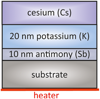 | ||
| Fig. 7 Schematic overview of a typical layer sequence for a K2CsSb photocathode, based on the original approach taken from ref. 51. | ||
Any adsorption of gases like H2, O2, CO, CO2 or H2O will poison the photoemissive layer and disturb the crystal lattice, leading to a reduced QE.104
The key parameter of this type of cathode was the K layer thickness that was studied by BNL.51 The highest QE was achieved with a Sb![[thin space (1/6-em)]](https://www.rsc.org/images/entities/char_2009.gif) :K ratio of 1:2.2, which means 10 nm Sb and about 22 nm K was deposited. A longer deposition of K would lead to the formation of tri-potassium antimony (K3Sb) that prevents the subsequent diffusion of deposited Cs.
:K ratio of 1:2.2, which means 10 nm Sb and about 22 nm K was deposited. A longer deposition of K would lead to the formation of tri-potassium antimony (K3Sb) that prevents the subsequent diffusion of deposited Cs.
The freshly prepared cathode could be transported in a UHV suitcase into the SRF Gun. During the transportation the cathode lost some QE that was caused by vacuum instabilities. Despite of this loss, the remained QE was still sufficient enough for the applications in SRF guns. Seen as a suggestion, a preparation next to the injector reduces the transportation difficulties and can be beneficial for the QE of the photocathode.
The main difference between the cathodes from Wang et al. was the diameter size of the deposited bi-alkalides on the substrate surface. The cathode where the entire 20 mm substrate surface was covered by K2CsSb showed high multi-pacting and degraded fast, which meant a fast exponential decay in the QE. Additionally, a degradation in the SRF gun performance was also recognized, which was related to the release of photocathode incidences into the cavity downstream. Nevertheless, the group showed that the cathodes survived at least 20 days in the SRF gun.51
Summarizing, K2CsSb cathodes have many advantages due to their high QE and low thermal emittance. Nevertheless, the difficulties related to the complex preparation with the precise ratio of an optimal composition in order to gain a high QE and a long lifetime should be taken into account. One should also consider the limited lifetime under RF fields and the potential risk of cavity contamination, when used in (S)RF injectors.
5.3 Gallium arsenide
In contrast to Cs2Te and K2CsSb photocathodes, GaAs and GaN semiconductors are already grown on a substrate. Both semiconductors are commercially available with reproducible quality which is a benefit as the desired quality and the dopant concentrations can be guaranteed by the supplier.GaAs is a semiconductor with a zinc blende structure and a direct band gap, which makes the photo-excitation energetically more favorable as in case of indirect band gap semiconductors. For the photoemission, p-doping is needed, which means that one lattice site of the original host atom is replaced to an atom with one valence electron less. This causes the appearance of holes in the lattice structure. Another benefit of the p-doping is its responsibility to introduce band bending, shown in Fig. 8. The p-doping lowers the CB, thus reducing the EA energy. With the deposition of Cs on the surface, the Evac can be lowered to the same energy level as the CB. Therefore it is not possible for photoelectrons to enter into the vacuum. By adding a strong electronegative oxidant such as O2 or nitrogen tri-fluoride (NF3) the Evac can be further reduced below the CBM and photoelectrons will now be able to leave the GaAs surface (Fig. 8).108,109
 | ||
| Fig. 8 Schematic drawing of the band structure of p-GaAs, activated in a YoYo process with Cs and O2. | ||
Since Scheer and Laar proposed GaAs as a photoemitter,110 this material found broad applications in photodetectors,111 electron microscopes112 and photon-enhanced thermionic emission devices.113 Its good spectral response to near infrared (NIR) and low dark current makes it suitable to vacuum photodetectors. The possibility to reach a high current density under excitation by visible lasers, spin-polarization, low thermal emittance and a narrow energy distribution fit to the requirements of high brightness electron sources for FEL, energy recovery lines (ERL) and THz devices.114 GaAs absorbs a broad wavelength spectrum and has the ability to emit spin-polarized photoelectrons when illuminated with polarized NIR light.108 The emission of spin-polarized electrons represents the main advantage and plays an increasing role in high energy physics. The spin-polarized electrons are used in combination with accelerator technology in transmission electron microscopy when using GaAs superlattices in order to create magnetic field images with high resolutions.5
A faster response time and a high spin-polarization electron yield was recently achieved by a gallium arsenide phosphide (GaAsP) superlattice photocathode.115 The rapid development in the research on GaAs/GaAsP superlattice photocathodes offers new research fields for more advanced semiconductor photocathodes and their potential application as an electron source.
An alternative to wet chemical cleaning represents ion-sputtering that allows to achieve an atomically clean surface.120 This technique uses energetic ions, such as argon (Ar+) or hydrogen (H+), bombarding the semiconductor surface in order to remove surface adsorbates. The disadvantage of ion sputtering lies in the potential risk of surface damage, decomposition and higher surface roughness.121
However, the more usual way is to thermally clean the GaAs surface at 500–600 °C for minimum half an hour in UHV environment. As already mentioned before, the aim of the thermal cleaning is to obtain a chemically clean and uniform GaAs surface, which can be examined by ex situ or in situ surface studies, such as X-ray photoelectron spectroscopy (XPS).
Togawa et al. showed that GaAs was activated in a so-called YoYo process, after it has been thermally cleaned.122 The YoYo process consisted of the sequential deposition of Cs and O2 to receive a NEA surface, shown in Fig. 9. The deposition process was monitored by a in situ photocurrent measurement. At first Cs was deposited excessively which was recognized by the descending photocurrent. Afterwards O2 was added to the excessively cesiated surface. When the photocurrent reached a maximum and started to drop again, the deposition of O2 was stopped. Each step of Cs and O2 deposition was repeated several times until a final photocurrent was achieved. Other oxidative gases such as NF3 could also be considered as a successful activation ingredient besides O2.123
 | ||
| Fig. 9 Schematic drawing of a typical photocurrent evolution when a YoYo activation is used (alternately applying Cs and O2). | ||
There is no clear recipe for the GaAs preparation as different facilities follow different activation conditions. Some researchers prefer to deposit Cs all the time and just turn on O2 occasionally to increase the photocurrent when it is needed.69 Therefore this method represents more a co-deposition, rather than a sequential deposition.
Recent investigations dealed with the theory of a dipole model of Ga–O–Cs and its relevance to form a NEA surface.124–126 Furthermore, the importance of a clean GaAs surface was discussed in 2020.119 Since photocathode research started, it was well known that the surface cleanness has a great influence on the photoemission performance. As mentioned in the sections above, the surface can be contaminated easily with various organic substances, oxides and air components. Therefore, Zhang et al. studied the p-GaAs performance depending on different cleaning processes.127 The surface composition and its potential contaminations hindered the Cs/O2 deposition to form a NEA surface. Therefore, it was impossible to form a proper Ga–O–Cs dipole layer if contaminants remained on the surface. Consequently, the photoemission performance was less than expected.
The QE of GaAs is affected by many other factors than those discussed in the sections above. Beside vacuum, material quality, incident wavelength, cathode temperature, Schottky effect and surface contaminations, the thickness of the GaAs layer, dopant concentration and NEA conditions play an immense role for the successful operation of this material. Therefore, the optimization of this material is still a hot topic in modern research.
However, it should be pointed out that GaAs photocathodes show the lowest thermal emittance value compared to other known photocathodes. Regarding to the thermal emittance, our analysis of the literature data shows that further research on these issues is strongly demanded.
One problem of GaAs photocathodes is the variation of the response time with the wavelength of the incident light. The penetration depth of the incident light depends on its wavelength. Near the band gap photoelectrons are generated deep in the material. The deeper the photoelectrons are generated in the material, the longer they need to travel towards to the surface. In fact this means that a longer extraction time gives them more time to thermalize and therefore they do not contribute anymore to the QE. Therefore, a thin layer of GaAs on a glass substrate, operating in transmission mode, is used to overcome this problem.131
In the last years, research was carried out to protect the GaAs emission layer with a Cs2Te116,129 or a Cs–Sb protection layer.132 The Cs2Te protection layer was able to extend the lifetime of GaAs significantly, resulting in a five times slower QE decay than for GaAs photocathodes without such a protection layer.133
 | ||
| Fig. 10 Schematic drawing of the difference in the incident light paths in a transmission (left) and reflection mode (right) GaAs photocathode. | ||
Contrary, in the reflective mode the photocathode is illuminated from the frontside with the incident light. Both techniques are illustrated in Fig. 10 where photoelectrons are generated and travel in all directions through the GaAs layer.
 | ||
| Fig. 11 Schematic representation of the electron transitions for the generation of spin-polarized electrons in GaAs photocathodes. | ||
The energy difference of these levels is 0.34 eV and the electron transition rule is Δm = ±1. This means m is for positive helicity light +1 and for negative helicity light −1. Some transitions are more favourable than others and thus the probability for positive helicity light is three times higher as more electrons are lifted into the m = −1/2 state than into the m = +1/2 state.135 When electrons are excited from the spin–orbit-splitt-off band, no polarization occurs at all. In contrast, a maximum polarization is obtained for a photon energy exceeding the band gap energy for less than 0.1 eV. A big advantage is the easily achievable polarization reversibility as the incident irradiation can be changed externally.
The main drawback of GaAs for high polarization is its reduced QE. Usually the electron spin-polarization yield (ESP) is between 30–50%, depending on dopant concentration, temperature and the operation mode for unstrained bulk GaAs.136,137 Demonstrations at SLAC showed that a polarization yield up to 80% was achieved with high-gradient doped strained GaAs.138 However, the highest polarization yield of 84% at 6.4% QE was reported on superlattice structured GaAs with a distributed Bragg reflector (DBR).139
To sum up, GaAs is the only photocathode at the moment which is able to produce spin-polarized electrons. Its spectral response in NIR is advantageous because no UV laser is needed. On the other side GaAs as a photocathode has many disadvantages such as the complex activation with alternatively Cs and O2. One should also consider the very strict requirement on stable UHV vacuum conditions. The limited lifetime and the risk of multi-pacting and its consequences are very high when the photocathode is used in a RF field. Thus, more studies regarding this issue are necessary.
5.4 Gallium nitride
III-Nitride semiconductors are widely used for blue, green and UV light-emitting diodes.140 The adsorption range in UV- and visible light characterizes these compound materials as potential photocathodes. GaN as a photocathode is expected to be robuster and can achieve a higher QE than other photocathodes.141 The potential application in particle accelerator injectors is quite new and up to now not tested.The rapid development in semiconductor industry offer improved growth methods and new possibilities to manufacture structured photocathodes. The variation of the dopant concentration inside the emission layer in combination with different layer thicknesses have a high impact on the performance of the semiconductor photocathodes. This multi-variability of the growth and doping methods makes a reliable comparison of photocathodes prepared by different groups at different facilities very difficult.
As a rule, usually Mg-doping is used to create a p-type GaN semiconductor and an optimal hole concentration of 1017 cm−3 is desired to achieve high QE.142 Some publications refer to the Mg concentration instead of the hole concentration, whereby the hole concentration is estimated to be two orders of magnitude lower than the introduced Mg concentration.143
The highest QE for GaN-based photocathodes was reported by Uchiyama et al. where about 70% QE could be achieved depending on the p-dopant concentration.143 This result showed that an optimal Mg dopant concentration was strongly required because it was beneficial for the photoelectrons to travel towards the surface.
The uniform-doping is widely applied in semiconductors, however, the photocathode performance can be increased with gradient-,144 exponential-145 and delta-doping146,147 profiles. This possibility pushes the rapid development of advanced efficient GaN photocathodes because two times higher QE was achieved with gradient-doped GaN than with uniform-doping.144
Another important variable that has to be considered is the thickness of the buffer and emission layer. Nitride semiconductors are usually produced by metal–organic chemical vapor deposition (MOCVD), molecular beam epitaxy (MBE) or other physical deposition processes like magnetron sputtering (MSE).140 Usually, a single crystal or hetero-epitaxial thin film is grown on a substrate such as silicon (Si), sapphire (Al2O3), silicon carbide (SiC) or spinel (MgAl2O4). The most commonly used substrate is Al2O3 because of its availability and low cost. Unfortunately, Al2O3 is not the substrate of choice because of the high lattice mismatch between Al2O3 and GaN of 16–17%, whereas GaN on SiC has only a lattice mismatch of 3%.148,149 A high crystal quality with low lattice mismatch is necessary to guarantee a photocathode with high QE. Therefore often buffer layers (aluminum nitride (AlN), Ga1−xAlxN or undoped GaN) of different thicknesses were grown on the substrate to reduce the lattice mismatch.
Additionally, the emission layer thickness plays an important role to achieve higher QE with nanostructured photocathodes. An optimal thickness guarantees the full absorption of the incident light without losing photoelectrons on their way to the surface. Different layer thicknesses were compared in transmission and reflection mode photocathodes.150,151 The optimal emission layer thickness was found between 90–200 nm.142 p-GaN nanowire photocathodes show higher QE than planar p-GaN photocathodes.152 Xia et al. showed that the QE can be even further increased by using exponentially doped GaN nanowires.153
In the last years, graphene was found to be a potential new substrate for bi-alkali photocathodes.154 The graphene substrate could be reused after an annealing at 500 °C and the renewed bi-alkali photocathode achieved similar QE values in the renewed process. Yayama et al. grew 2D GaN on a thin graphene sheet, supported by bulk GaN.155 The suggested growth method leads to 2D GaN possessing novel advanced electronic properties. The introduction of a thin graphene sheet could also reduce the high lattice mismatch between GaN and other substrates, such as the widely used Al2O3 or Si. The cut-off spectral response for p-GaN photocathodes is usually at 360 nm156 and thus a little relief of the UV-laser system can be guaranteed. However, the spectral response is adjustable by the manipulation of the Egap with suitable dopant atoms. These dopants, such as indium (In) or phosphorous (P) can decrease the Egap to a more suitable wavelength in the visible spectral range and recently published studies reported on the potential usage of such novel InGaN photocathodes.157–159
An activation with a thin alkali metal layer like Cs reduces the surface work function of GaN to form a NEA surface. As a consequence, the Evac is shifted below the CBM energy level. Electrons excite over the Egap and can easily enter into the vacuum, shown in Fig. 12.
 | ||
| Fig. 12 Schematic representation of the band structure of p-GaN when activated with Cs and O2. | ||
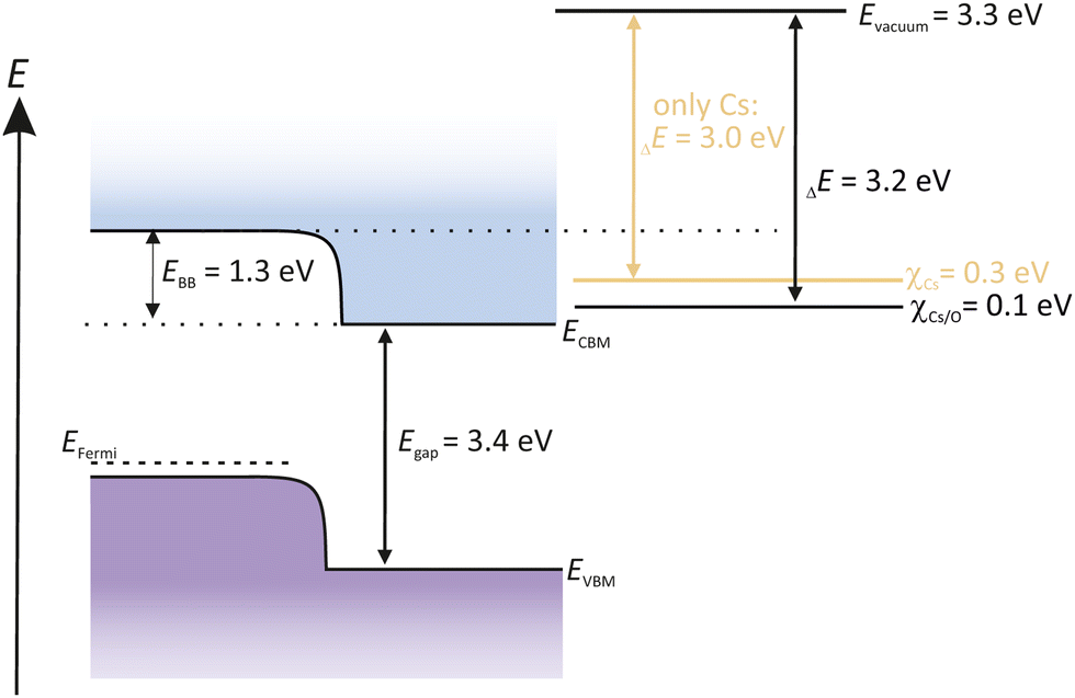
Many studies were carried out recently dealing with the photoemission of GaN and the role of O2 in its activation process.109,162 It is widely accepted that the activation of GaN and GaAs photocathodes are different. Wang et al. reported that an activation of GaN with sequential Cs/O2 gave no significant improvement compared to an activation with only Cs. When using Cs excessively, like in the YoYo process, it was assumed that more than a monolayer of Cs deposits onto the GaN surface. Consequently, the photocurrent decreased. If afterwards O2 was introduced to the Cs-poisoned GaN surface, the photocurrent increased again, and the alternating cycle can be repeated until the photocurrent reached a maximum value.
The reason why O2 is assumed to be not beneficial for GaN photocathodes, lays in the EA potential. When introducing Cs to the GaN surface, Evac is reduced down to 3 eV. The new position of the Evac is then already below the CBM. The Evac can be only further 0.2 eV reduced when O2 is introduced. Therefore, O2 has no obvious benefit and thus is not necessary to obtain a NEA surface for GaN semiconductors.163 In fact, this means that the activation for GaN with only Cs is more practicable and easier, compared to other photocathodes, such as GaAs or Cs2Te.
Amano et al. studied the QE recovery of Cs/O2 activated p-GaN on Al2O3 and as-received n-GaAs by a thermal cleaning.125 GaN was thermally cleaned at 500 °C and 600 °C and activated by a sequential Cs/O2 deposition of a YoYo process. In this research the fresh photocathode was exposed to N2, which lowered the QE three orders of magnitude. 60% of the initial QE was recovered with a new subsequential thermal cleaning. Thus, it is obvious that the re-activation of NEA cathodes is possible, but further studies are strongly recommended.
An efficient and permanent heat dissipation is necessary to keep the cathode at convenient temperatures. To bypass the thermal conductivity problem of the substrate, Schumacher et al. investigated the deposition of p-GaN on Cu using a sputter magnetron method.164 Cu provides a good thermal conductivity and should be considered as a potential substrate for GaN. To overcome the high lattice mismatch between GaN and Cu, an AIN buffer layer was introduced.
Summarizing, GaN shows an enormous potential as a future novel electron source in particle accelerators. Although p-GaN requires UV light like many other photocathodes, its spectral response is adjustable by the manipulation of the Egap with suitable dopant atoms. Furthermore, p-GaN can be easier prepared as compared to other semiconductor cathodes, and it is possible to simplify its activation by applying exclusively Cs. A big advantage is the possibility to juvenile this cathode with a subsequent thermal treatment to remove the adsorbed pollutants from the surface when the photocathode degraded.
In the last year, a new idea of using non-activated GaN for spin-polarized electrons showed up.165 The reason why GaN has the ability to produce spin-polarized electrons lies in its wurtzite crystal structure. The ongoing research has the aim to detach the highly sensitive GaAs-based photocathodes.
Furthermore, a more detailed information about GaN-based photocathodes can be found in a recently published review.142
6 Other photocathode ideas
A new idea is to use photocathodes with nano diamond layers, which can guarantee a higher QE than metal photocathodes.166 The production with a pulsed spray technique is easier and has more advantages compared to CVD methods that need a hot substrate. With this new technique the nano diamond layers are deposited directly from a dispersion solution at low temperatures onto a substrate.Another novel idea is the usage of titanium nitride (TiN) photocathodes, which seem to be promising for photoinjectors because they provided a prompt response time and a low thermal emittance as shown by An et al.167 Unfortunately, the TiN photocathodes showed a low QE, which was assumed to derive from an O2 or other surface contamination. By creating an atomically clean surface or by using a nanostructured TiN photocathode the QE could be potentially increased.
7 Conclusion and outlook
This paper summarizes the development of the existing photocathodes that are mostly used in particle accelerator photoinjectors.Metal photocathodes such as Mg, Cu and Pb are simple in their surface cleaning which makes them easy to handle. Their biggest advantage is their high robustness against vacuum instabilities compared to semiconductor photocathodes. Even in case of surface oxidation, they can be rejuvenated after another surface cleaning. Their high work function makes them less efficient, and the strong desire of higher beam current leads to the usage of semiconductor photocathodes. However, a robust metal cathode is the first choice for the commissioning of an photoinjector.
Besides metal cathodes, semiconductors such as Cs2Te and K2CsSb are the most commonly used photocathodes in particle accelerators. They provide high QE of above 10%, which makes them highly attractive. However, they are very sensitive to any vacuum instabilities and represent a risk for a potential contamination in the photoinjector due to the release of compound atoms. Moreover, the preparation of semiconductor photocathodes, consisting of a deposition of different compound materials on a substrate is more complicated than the simple cleaning of metal cathodes. One should take into account that even under the same conditions in the same laboratory the cathode quality can vary, depending on the quality of the semiconductor produced.
A special type of semiconductor photocathodes represent the III–V semiconductors, such as GaAs and GaN. These semiconductors are already grown on a substrate and commercially available. In order to produce a photocathode only a thin film deposition of Cs (and O2) is needed.
GaAs is the cathode of choice if a spin-polarized beam or a low thermal emittance is desired. The preparation of the GaAs photocathode requires an alternate application of Cs and an electronegative component like O2. The QE of GaAs resembles to those of other semiconductors, depending on the incident wavelength. A compromise between a high QE and a polarization rate has to be found because only one can be high while the other is low. The disadvantage of this cathode type is its short lifetime of approximately one hundred hours and also its potential release of Cs or other compounds into the injector system. Thus, the research for improving the lifetime of a GaAs photocathode is still ongoing.
Similar to GaAs, p-GaN can form a NEA surface to obtain a photocathode. A reported QE in the range of 40–70% is a good foundation for further research of this novel type of photocathode. None of the used cathodes in particle accelerators can provide such high QE values so far. Although p-GaN requires UV light, it guarantees a more stable NEA layer with less stringent vacuum conditions. With the possibility of modulating the Egap by dopants such as In or P the requirements of the laser system could be relieved. Therefore, p-GaN photocathodes with a robust NEA layer show a high potential for high current applications. However, not all necessary parameters have been studied so far. Actual data about thermal emittance and response time are missing or need to be updated.
Further investigations have to be carried out on p-GaN photocathodes with the possibility of using much higher crystal quality and an optimal doping rate in p-GaN layers nowadays.
p-GaN and its nanostructures show an enormous potential, reaching high QE and promise more robustness. Operational parameters and the information about its behavior in the injector system are not available at the moment, but they are required for advanced electron beam sources.
A future possibility for improving semiconductor photocathodes is to change the surface composition to stabilize or protect the emission layer. Cs:F:Li168 or Cs:O:Sb169 can be used to form a protection layer on GaAs photocathodes. Alternatively, Cs2Te can also be considered as a protective layer for GaAs as already mentioned in Section 5.3.4.116,129
In the last years, detailed studies were carried out to explore the influence of a thin graphene layer on the performance of metals and bi-alkali photocathodes.170–172 These studies report that both photocathodes have a good compatibility leading to a high crystallinity of the emission layer.173 The application of two monolayers of graphene achieved the highest QE with a homogenous distribution.171 Besides graphene as a potential coating, the idea of a boron nitride (BN) or molybdenum sulfide (MoS2) coating for photocathode arose.174 Wang et al. found out that a monolayer of BN maintains the QE, making it an ideal coating material for alkali-based semiconducting photocathodes. This study additionally considered a few layers of graphene or MoS2 as a useful protection layer but with the disadvantage that those coatings increase the work function of the alkali-based photocathode.
The new avenues opened by the above mentioned coating techniques contribute to the future development of photocathode materials. Simulations and advanced analytical chemistry are necessary to understand the physics and chemistry of the coated photocathodes to guarantee a fabrication of high performance photocathodes for future electron-beam applications.
The improving crystal quality, the optimization of growth conditions and the application of new low-dimensional materials, such as 2D sheets, nanowires and nanotubes push the development of semiconductor photocathodes towards their application in high power devices, detectors and electron source in particle accelerators.
Conflicts of interest
There are no conflicts to declare.Acknowledgements
This research did not receive any specific grant from funding agencies in the public, commercial, or not-for-profit sectors. The authors would like to thank P. Michel and the ELBE team, especially the SRF Gun group for their support. Special thanks goes to all who proofread the manuscript.References
- M. Krysztof, Microsyst. Nanoeng., 2021, 7, 00268 CrossRef PubMed.
- P. W. Hawkes and J. C. Spence, Science of Microscopy, Springer, 2007, vol. 1 Search PubMed.
- L. Zhao, J. Wu, Z. Wang, H. Tang, X. Zou, T. Jiang, P. Zhu, D. Xiang and J. Zhang, Struct. Dyn., 2021, 044303 CrossRef CAS PubMed.
- J. F. Dawson, A. C. Marvin and C. A. Marshman, Electromagnetic Compatibility, Encycl. Phys. Sci. Technol., 2003, vol. 3, pp. 261–275 Search PubMed.
- G. Gaertner, W. Knapp and R. G. Forbes, Modern Developments in Vacuum Electron Sources, Springer, 2020 Search PubMed.
- S. V. Kutsaev, Tech. Phys., 2021, 66, 161–195 CrossRef CAS.
- T. Rao and D. H. Dowell, An Engineering Guide to Photoinjectors, Createspace Independent Publishing Platform, 2013 Search PubMed.
- A. T. Odularu, J. Spectrosc., 2020, 8868713 Search PubMed.
- A. T. Khotbeh-sara, F. Rahmani and F. Ghasemi, Radiat. Phys. Eng., 2021, 2, 9–17 Search PubMed.
- A. G. Kazakov, T. Y. Ekatova and J. S. Babenya, J. Radioanal. Nucl. Chem., 2021, 328, 493–505 CrossRef CAS.
- E. Sobolev, S. Zolotarev and K. Giewekemeyer, Commun. Phys., 2020, 3, 0362 Search PubMed.
- D. Khakhulin, F. Otte, M. Biednov, C. Bömer, T. K. Choi, M. Diez, A. Galler, Y. Jiang, K. Kubicek, F. A. Lima, A. Rodriguez-Fernandez, P. Zalden, W. Gawelda and C. Bressler, Appl. Sci., 2020, 10, 995 CrossRef CAS.
- S. Kovalev, K. J. Tielrooij, J. C. Deinert, I. Ilyakov, N. Awari, M. Chen, A. Ponomaryov, M. Bawatna, T. V. de Oliveira, L. M. Eng, K. A. Kuznetsov, D. A. Safronenkov, G. K. Kitaeva, P. I. Kuznetsov, H. A. Hafez, D. Turchinovich and M. Gensch, npj Quantum Mater., 2021, 6, 84 CrossRef.
- S. V. Baryshev, E. Wang, C. Jing, V. Jabotinski, S. Antipov, A. D. Kanareykin, S. Belomestnykh, I. Ben-Zvi, L. Chen, Q. Wu, H. Li and A. V. Sumant, Appl. Phys. Lett., 2021, 118, 053505 CrossRef CAS.
- L. Cultrera, E. Rocco, F. Shahedipour-Sandvik, L. D. Bell, J. K. Bae, I. V. Bazarov, P. Saha, S. Karkare and A. Arjunan, J. Appl. Phys., 2022, 131, 124902 CrossRef CAS.
- P. Tripathi, A. Kumar, S. Dwivedi and P. K. Jain, IEEE Trans. Plasma Sci., 2020, 48, 438–445 Search PubMed.
- B. Dunham, J. Barley, A. Bartnik, I. Bazarov, L. Cultrera, J. Dobbins, G. Hoffstaetter, B. Johnson, R. Kaplan, S. Karkare, V. Kostroun, Y. Li, M. Liepe, X. Liu, F. Loehl, J. Maxson, P. Quigley, J. Reilly, D. Rice, D. Sabol, E. Smith, K. Smolenski, M. Tigner, V. Vesherevich, D. Widger and Z. Zhao, Appl. Phys. Lett., 2013, 102, 98–102 CrossRef.
- O. Tanaka, T. Miyajima and N. Higashi, Proc. IPAC2021, 2021, pp. 4531–4534 Search PubMed.
- F. Hug, K. Aulenbacher, S. Friederich, P. Heil, R. G. Heine, R. Kempf, C. Matejcek and D. Simon, 63th ICFA Adv. Beam Dyn. Energy Recover, Linacs, ERL2019, Berlin, 2021, pp. 14-17.
- A. Lueangaramwong, X. Li, P. Boonpornprasert, O. Lishilin, M. Krasilnikov, Z. Aboulbanine, G. Adhikari, N. Aftab, N. Chaisueb, G. Georgiev, J. Good, M. Gross, C. Koschitzki, D. Melkumyan, H. Qian, G. Shu, G. Vashchenko, T. Weilbach, F. Stephan, D. Zeuthen and H. Shaker, Proc. of 12th Int. Part. Acc. Conf. 2021 (IPAC2021), 2021, pp. 3285-3288.
- Y. D. Kluchevskaia and S. M. Polozov, Cybern. Phys., 2020, 9, 98–102 Search PubMed.
- C. C. Xiao, J. Q. Zhang, J. H. Tan and W. C. Fang, Nucl. Sci. Technol., 2020, 31, 100 CrossRef.
- R. Xiang, A. Arnold, P. Michel, P. Murcek, J. Teichert, P. Lu and H. Vennekate, IPAC 2014 Proc. 5th Int. Part. Accel. Conf., 2014, pp. 642-644.
- I. Petrushina, V. N. Litvinenko, Y. Jing, J. Ma, I. Pinayev, K. Shih, G. Wang, Y. H. Wu, Z. Altinbas, J. C. Brutus, S. Belomestnykh, A. Di Lieto, P. Inacker, J. Jamilkowski, G. Mahler, M. Mapes, T. Miller, G. Narayan, M. Paniccia, T. Roser, F. Severino, J. Skaritka, L. Smart, K. Smith, V. Soria, Y. Than, J. Tuozzolo, E. Wang, B. Xiao, T. Xin, I. Ben-Zvi, C. Boulware, T. Grimm, K. Mihara, D. Kayran and T. Rao, Phys. Rev. Lett., 2020, 124, 244801 CrossRef CAS PubMed.
- D. H. Dowell, I. Bazarov, B. Dunham, K. Harkay, C. Hernandez-Garcia, R. Legg, H. Padmore, T. Rao, J. Smedley and W. Wan, Nucl. Instrum. Methods Phys. Res., Sect. A, 2010, 622, 685–697 CrossRef CAS.
- F. Hug, K. Aulenbacher, D. Simon, C. P. Stoll and S. D. W. Thomas, 63th ICFA Adv. Beam Dyn. Energy Recover, Linacs, ERL2019, Berlin, 2020, pp. 28-33.
- Z. T. Zhao, Z. Wang, C. Feng, S. Chen and L. Cao, Sci. Rep., 2021, 11, 23875 CrossRef CAS PubMed.
- N. Nishimori, I. Bazarov and B. Dunham, Proc. ERL09, 2009, pp. 6–23 Search PubMed.
- J. Teichert, A. Arnold, G. Ciovati, J.-C. Deinert, P. Evtushenko, M. Justus, P. Kneisel, S. Kovalev, M. Kuntzsch, U. Lehnert, P. Lu, S. Ma, P. Murcek, P. Michel, A. Ryzhov, J. Schaber, C. Schneider, R. Schurig, R. Steinbrück, H. Vennekate, I. Will and R. Xiang, Phys. Rev. Accel. Beams, 2021, 24, 033401 CrossRef CAS.
- I. V. Bazarov, B. M. Dunham, X. Liu, M. Virgo, A. M. Dabiran, F. Hannon and H. Sayed, J. Appl. Phys., 2009, 105, 0837151 CrossRef.
- R. Xiang and J. Teichert, Phys. Procedia, Int. Conf. Laser Appl. Accel. (LA3NET) 2015, 2015, pp. 58-65.
- A. Kahn, Mater. Horiz., 2016, 3, 7–10 RSC.
- D. H. Dowell and J. F. Schmerge, Phys. Rev. Spec. Top. – Accel. Beams, 2009, 12, 074201 CrossRef.
- G. Gevorkyan, S. Karkare, S. Emamian, I. V. Bazarov and H. A. Padmore, Phys. Rev. Accel. Beams, 2018, 21, 093401 CrossRef CAS.
- S. Karkare and I. Bazarov, Phys. Rev. Appl., 2015, 4, 024015 CrossRef.
- A. Galdi, J. Balajka, W. J. DeBenedetti, L. Cultrera, I. V. Bazarov, M. A. Hines and J. M. Maxson, Appl. Phys. Lett., 2021, 118, 244101 CrossRef CAS.
- S. Matsuba, Y. Honda, X. Jin, T. Miyajima, M. Yamamoto, T. Uchiyama, M. Kuwahara and Y. Takeda, Jpn. J. Appl. Phys., 2012, 51, 046402 CrossRef.
- P. W. Huang, W. H. Huang and C. X. Tang, Proc. 38th Int. Free. Laser Conf. (FEL 2017), 2017, pp. 394-396.
- D. H. Dowell, F. K. King, R. E. Kirby, J. F. Schmerge and J. M. Smedley, Phys. Rev. Spec. Top. – Accel. Beams, 2006, 9, 063502 CrossRef.
- A. di Bona, F. Sabary, S. Valeri, P. Michelato, D. Sertore and G. Suberlucq, J. Appl. Phys., 1998, 80, 3024 CrossRef.
- H. Iijima, M. Kuriki and Y. Masumoto, 2nd Int. Part. Accel. Conf. 2011 (IPAC 2011), 2011, pp. 3158-3160.
- D. K. Schroder, N. R. Thomas, J. Vine and H. Nathanson, Trans. Electron Dev., 1974, 21, 785–798 Search PubMed.
- J. Shao, J. Shi, S. P. Antipov, S. V. Baryshev, H. Chen, M. Conde, W. Gai, G. Ha, C. Jing, F. Wang and E. Wisniewski, Phys. Rev. Lett., 2016, 117, 084801 CrossRef PubMed.
- D. Sertore, S. Schreiber, K. Floettmann, F. Stephan, K. Zapfe and P. Michelato, Nucl. Instrum. Methods Phys. Res., Sect. A, 2000, 445, 422–426 CrossRef CAS.
- J. H. Han, J. Bähr, H. J. Grabosch, M. Krasilnikov, V. Miltchev, A. Oppelt, B. Petrosyan, S. Riemann, L. Staykov, F. Stephan, M. V. Hartrott, K. Flöttmann, S. Schreiber, J. Rönsch, P. Michelato, L. Monaco and D. Sertore, Proc. of IEEE Part. Accel. Conf., 2005, pp. 895-897.
- A. Aryshev, M. Shevelev, Y. Honda, N. Terunuma and J. Urakawa, Appl. Phys. Lett., 2017, 111, 033508 CrossRef.
- L. Cultrera, I. Bazarov, A. Bartnik, B. Dunham, S. Karkare, R. Merluzzi and M. Nichols, Appl. Phys. Lett., 2011, 99, 152110 CrossRef.
- L. Cultrera, J. Maxson and I. Bazarov, Phys. Rev. ST Accel. Beams, 2011, 14, 120101 CrossRef.
- C. Hernandez-Garcia, B. Bullard, J. Benesch, J. Grames, J. Gubeli, F. Hannon, J. Hansknecht, J. Jordan, R. Kazimi, G. A. Krafft, M. A. Mamun, M. Poelker, M. L. Stutzman, R. Suleiman, M. Tiefenback, Y. Wang, S. Zhang, C. A. Valerio Lizarraga, R. Montoya Soto and A. Canales Ramos, Phys. Rev. Accel. Beams, 2019, 22, 113401 CrossRef CAS.
- R. Xiang, A. Arnold, P. Lu, P. Murcek, J. Teichert and H. Vennekate, Proc. of IPAC 2018, 2018, pp. 4142-4144.
- E. Wang, V. N. Litvinenko, I. Pinayev, M. Gaowei, J. Skaritka, S. Belomestnykh, I. Ben-Zvi, J. C. Brutus, Y. Jing, J. Biswas, J. Ma, G. Narayan, I. Petrushina, O. Rahman, T. Xin, T. Rao, F. Severino, K. Shih, K. Smith, G. Wang and Y. Wu, Sci. Rep., 2021, 11, 4477 CrossRef CAS PubMed.
- Y. Zhou and P. Zhang, J. Appl. Phys., 2020, 127, 164903 CrossRef CAS.
- W. E. Spicer, Phys. Rev., 1958, 112, 114 CrossRef CAS.
- S. Karkare, D. Dimitrov, W. Schaff, L. Cultrera, A. Bartnik, X. Liu, E. Sawyer, T. Esposito and I. Bazarov, J. Appl. Phys., 2013, 113, 104904 CrossRef.
- X. Y. Wu, H. Liang, M. F. Ciappina and L. Y. Peng, Photonics, 2020, 7, 129 CrossRef.
- O. Chubenko, S. Karkare, D. A. Dimitrov, J. K. Bae, L. Cultrera, I. Bazarov and A. Afanasev, J. Appl. Phys., 2021, 130, 063101 CrossRef CAS.
- Z. Jiang, Q. Gu, X. Li, E. Wang, M. Gaowei and W. Liu, Phys. Rev. Accel. Beams, 2021, 24, 33402 CrossRef CAS.
- E. R. Antoniuk, Y. Yue, Y. Zhou, P. Schindler, W. A. Schroeder, B. Dunham, P. Pianetta, T. Vecchione and E. J. Reed, Phys. Rev. B, 2020, 101, 235447 CrossRef CAS.
- C. Metzger, M. Graus, M. Grimm, G. Zamborlini, V. Feyer, M. Schwendt, D. Lüftner, P. Puschnig, A. Schöll and F. Reinert, Phys. Rev. B, 2020, 101, 165421 CrossRef CAS.
- R. Amador and H.-d Saßnick, J. Phys.: Condens. Matter, 2021, 33, 365502 CrossRef CAS PubMed.
- J. Krumland, A. M. Valencia, S. Pittalis, C. A. Rozzi and C. Cocchi, J. Chem. Phys., 2020, 153, 054106 CrossRef CAS PubMed.
- H.-D. Saßnick and C. Cocchi, Electron. Struct., 2021, 3, 027001 CrossRef.
- R. P. Xian, V. Stimper, M. Zacharias, S. Dong, M. Dendzik, S. Beaulieu, B. Schölkopf, M. Wolf, L. Rettig, C. Carbogno, S. Bauer and R. Ernstorfer, Nat. Comput. Sci., 2022, 1, 00382 Search PubMed.
- J. M. Howard, Q. Wang, E. Lee, R. Lahoti, T. Gong, M. Srivastava, A. Abate and M. S. Leite, arXiv, 2020, 03702, DOI:10.48550/arXiv.2010.03702.
- J. Westermayr and R. J. Maurer, Chem. Sci., 2021, 12, 10755–10764 RSC.
- L. Ward, A. Agrawal, A. Choudhary and C. Wolverton, npj Comput. Mater., 2016, 2, 16028 CrossRef.
- A. Talapatra, B. P. Uberuaga, C. R. Stanek and G. Pilania, Chem. Mater., 2021, 33, 845–858 CrossRef CAS.
- H. C. Wang, S. Botti and M. A. Marques, npj Comput. Mater., 2021, 7, 00481 Search PubMed.
- Y. Zhang, K. Zhang, S. Li, S. Li, Y. Qian, F. Shi, G. Jiao, Z. Miao, Y. Guo and Y. Zeng, J. Appl. Phys., 2020, 128, 173103 CrossRef CAS.
- F. Machuca, Z. Liu, Y. Sun, P. Pianetta, W. E. Spicer and R. F. W. Pease, J. Vac. Sci. Technol., B: Nanotechnol. Microelectron.: Mater., Process., Meas., Phenom., 2003, 21, 1863 CrossRef CAS.
- C. I. Wu and A. Kahn, J. Appl. Phys., 1999, 86, 3209–3212 CrossRef CAS.
- J. Kühn, M. Bürger, A. Frahm, A. Jankowiak, T. Kamps, G. Klemz, G. Kourkafas, P. Murcek, A. Neumann, N. Ohm, M. Schmeißer, M. Schuster, J. Teichert and J. Völker, Proc. of IPAC2018, 2018, pp. 1247-1250.
- L. B. Jones, D. P. Juarez-Lopez, B. L. Militsyn, C. P. Welsch and T. C. Q. Noakes, Proc. IPAC2018, 2018, pp. 4438-4441.
- J. Smedley, T. Rao and J. Sekutowicz, Phys. Rev. Spec. Top. – Accel. Beams, 2008, 11, 013502 CrossRef.
- B. Feuerbacher and B. Fitton, J. Appl. Phys., 1972, 43, 1563–1572 CrossRef CAS.
- A. A. Turnbull and G. B. Evans, J. Phys. D: Appl. Phys., 1968, 1, 155–160 CrossRef CAS.
- C. P. Hauri, R. Ganter, F. Le Pimpec, A. Trisorio, C. Ruchert and H. H. Braun, Phys. Rev. Lett., 2010, 104, 234802 CrossRef CAS PubMed.
- H. J. Qian, J. B. Murphy, Y. Shen, C. X. Tang and X. J. Wang, Appl. Phys. Lett., 2010, 97, 1–4 CrossRef.
- H. J. Qian, C. Li, Y. C. Du, L. X. Yan, J. F. Hua, W. H. Huang and C. X. Tang, Phys. Rev. Spec. Top. – Accel. Beams, 2012, 15, 040102 CrossRef.
- H. B. Michaelson, J. Appl. Phys., 1977, 48, 4729–4733 CrossRef CAS.
- L. A. J. Soomary, D. P. Juarez-Lopez, C. P. Welsch, L. B. Jones and T. C. Q. Noakes, Proc. of IPAC2021, 2021, pp. 2860-2862.
- S. Karkare, G. Adhikari, W. A. Schroeder, J. K. Nangoi, T. Arias, J. Maxson and H. Padmore, Phys. Rev. Lett., 2020, 125, 54801 CrossRef CAS PubMed.
- P. Michelato, Proc. of EPAC08, 2008, pp. 46-50.
- S. H. Kong, J. Kinross-Wright, D. C. Nguyen and R. L. Sheffield, Nucl. Instrum. Methods Phys. Res., Sect. A, 1995, 358, 272–275 CrossRef CAS.
- G. Suberlucq, Proc. of EPAC 2004, 2004, p. 602.
- Z. Yusof, A. Denchfield, M. Warren, J. Cardenas, N. Samuelson, L. Spentzouris, J. Power and J. Zasadzinski, Phys. Rev. Accel. Beams, 2017, 20, 123401 CrossRef.
- S. H. Kong, J. Kinross-Wright, D. C. Nguyen and R. L. Sheffield, J. Appl. Phys., 1995, 77, 6031–6038 CrossRef CAS.
- S. Ledere, J. H. Han, S. Schreiber, A. Vollmer, R. Ovsyannikov, M. Sperling, H. Duerr, F. Stephan, P. Michelato, L. Monaco, C. Pagani and D. Sertore, 29th Int. Free Electron Laser Conf. 2007 (FEL 2007), 2007, pp. 457-460.
- S. Lederer, S. Schreiber, P. Michelato, C. Pagani, D. Sertore, L. Monaco and J. Han, Proc. of EPAC08, 2008, pp. 232-234.
- S. Lederer, F. Brinker and S. Schreiber, Proc. 39th Int. Free. Laser Conf. 2019 (FEL 2019), 2019, pp. 427-429.
- L. Monaco, P. Michelato, D. Sertore, C. Pagani and G. Guerini Rocco, Proc. of 39th Int. Free. Laser Conf. 2019 (FEL 2019), 2019, pp. 297-300.
- P. Huang, H. Qian, Y. Chen, A. Grigoryan, M. Gross, I. Isaev, P. Kitisri, C. Koschitzki, M. Krasilnikov, S. Lal, X. Li, O. Lishilin, D. Melkumyan, R. Niemczyk, A. Oppelt, H. Shaker, G. Shu, F. Stephan, G. Vashchenko, T. Weilbach, S. Lederer, L. Monaco, P. Michelato and D. Sertore, Proc. of 39th Int. Free. Laser Conf. 2019 (FEL 2019), 2019, pp. 473-476.
- V. Miltchev, J. Baehr, H. J. Grabosch, J. H. Han, M. Krasilnikov, A. Oppelt, B. Petrosyan, L. Staykov, F. Stephan and M. V. Hartrott, Proc. of 27th Int. Free Electron Laser Conf. 2005 (FEL 2005), 2005, pp. 560-563.
- L. Zheng, J. Shao, E. E. Wisniewski, J. G. Power, Y. Du, W. Liu, C. E. Whiteford, M. Conde, S. Doran, C. Jing and C. Tang, Phys. Rev. Accel. Beams, 2020, 23, 52801 CrossRef CAS.
- K. Floettmann, TESLA FEL Rep., 1997, 97, 01 Search PubMed.
- R. Xiang, A. Arnold, P. Michel, P. Murcek and J. Teichert, Proc. of FEL2010, 2010, pp. 449-452.
- P. W. Huang, H. Qian, Y. Chen and D. Filippetto, Phys. Rev. Accel. Beams, 2020, 23, 43401 CrossRef CAS.
- F. Zhou, C. Adolphsen, A. Benwell, G. Brown, D. H. Dowell, M. Dunning, S. Gilevich, K. Grouev, G. Huang, B. Jacobson, X. H. Liu, A. Miahnahri, F. Sannibale, J. Schmerge and T. Vecchione, Phys. Rev. Accel. Beams, 2021, 24, 73401 CrossRef CAS.
- N. Chanlek, J. D. Herbert, R. M. Jones, L. B. Jones, K. J. Middleman and B. L. Militsyn, J. Phys. D: Appl. Phys., 2015, 48, 375102 CrossRef.
- G. Loisch, Y. Chen, C. Koschitzki, H. Qian, M. Gross, A. Hannah, A. Hoffmann, D. Kalantaryan, M. Krasilnikov, S. Lederer, X. Li, O. Lishilin, D. Melkumyan, L. Monaco, R. Niemczyk, A. Oppelt, D. Sertore, F. Stephan, R. Valizadeh, G. Vashchenko and T. Weilbach, Appl. Phys. Lett., 2022, 120, 104101 CrossRef.
- R. Xiang, A. Arnold, H. Buettig, D. Janssen, M. Justus, U. Lehnert, P. Michel, P. Murcek, A. Schamlott, C. Schneider, R. Schurig, F. Staufenbiel and J. Teichert, Phys. Rev. Spec. Top. – Accel. Beams, 2010, 13, 043501 CrossRef.
- S. Schreiber, S. Lederer, L. Monaco, D. Sertore and P. Michelato, Proc. of 38th Int. Free. Laser Conf. 2017 (FEL 2017), 2017, pp. 415-418.
- A. H. Sommer, Rev. Sci. Instrum., 1955, 26, 725–726 CrossRef CAS.
- M. A. Schmeißer, S. Mistry, H. Kirschner, S. Schubert, A. Jankowiak, T. Kamps and J. Kühn, Phys. Rev. Accel. Beams, 2018, 21, 113401 CrossRef.
- D. H. Dowell, K. J. Davis, K. D. Friddell, E. L. Tyson, C. A. Lancaster, L. Milliman, R. E. Rodenburg, T. Aas, M. Bemes, S. Z. Bethel, P. E. Johnson, K. Murphy, C. Whelen, G. E. Busch and D. K. Remelius, Appl. Phys. Lett., 1993, 63, 2035–2037 CrossRef CAS.
- I. Bazarov, L. Cultrera, A. Bartnik, B. Dunham, S. Karkare, Y. Li, X. Liu, J. Maxson and W. Roussel, Appl. Phys. Lett., 2011, 98, 224101 CrossRef.
- Y. Wang, M. A. Mamun, P. Adderley, B. Bullard, J. Grames, J. Hansknecht, C. Hernandez-Garcia, R. Kazimi, G. A. Krafft, G. Palacios-Serrano, M. Poelker, M. L. Stutzman, R. Suleiman, M. Tiefenback, S. Wijethunga, J. Yoskowitz and S. Zhang, Phys. Rev. Accel. Beams, 2020, 23, 103401 CrossRef CAS.
- X. Wang, Y. Zhang, H. Yu and J. Wu, Optik, 2016, 127, 7611–7624 CrossRef CAS.
- J. Ma, X. Fu, M. Yang, H. Zhao and S. Ren, Proc. of IEEE 4th Adv. Inf. Technol. Electron. Autom. Control Conf. 2019 (IAEAC 2019), 2019, pp. 1451-1455.
- J. J. Scheer and J. V. Laar, Solid State Commun., 1965, 3, 189–193 CrossRef CAS.
- X. Zhu, F. Lin, Z. Zhang, X. Chen, H. Huang, D. Wang, J. Tang, X. Fang, D. Fang, J. C. Ho, L. Liao and Z. Wei, ACS Appl. Mater. Interfaces, 2020, 20, 2654–2659 CAS.
- M. Kuwahara, S. Kusunoki, Y. Nambo, K. Saitoh, X. Jin, T. Ujihara, H. Asano, Y. Takeda and N. Tanaka, Appl. Phys. Lett., 2014, 105, 193101 CrossRef.
- L. Liu, Y. Diao and S. Xia, J. Mater. Sci., 2019, 54, 5605–5614 CrossRef CAS.
- G. L. Carr, M. C. Martin, W. R. McKinney, K. Jordan, G. R. Neil and G. P. Williams, Nature, 2002, 420, 153–156 CrossRef CAS PubMed.
- N. Scahill and K. Aulenbacher, J. Appl. Phys., 2022, 132, 185702 CrossRef CAS.
- J. Biswas, E. Wang, M. Gaowei, W. Liu, O. Rahman and J. T. Sadowski, AIP Adv., 2021, 11, 025321 CrossRef CAS.
- A. Özkartal and D. T. Noori, J. Mater. Sci.: Mater. Electron., 2021, 32, 13462–13471 CrossRef.
- I. Levchenko, V. Tomashyk, G. Malanych, I. Stratiychuk and A. Korchovyi, Appl. Nanosci., 2021, 12, 1139–1145 CrossRef.
- Y. Zhang, C. Fang, Y. Qian, J. Zhang, K. Zhang, J. Zhang, M. Rong, F. Shi, G. Jiao and X. Bai, Proc. SPIE, 2020, p. 54 Search PubMed.
- N. Razek, K. Otte, T. Chassé, D. Hirsch, A. Schindler, F. Frost and B. Rauschenbach, J. Vac. Sci. Technol., A, 2002, 20, 1492–1497 CrossRef CAS.
- G. Greczynski and L. Hultman, Appl. Surf. Sci., 2021, 542, 148599 CrossRef CAS.
- K. Togawa, T. Nakanishi, T. Baba, F. Furuta, H. Horinaka, T. Ida, Y. Kurihara, H. Matsumoto, T. Matsuyama, M. Mizuta, S. Okumi, T. Omori, C. Suzuki, Y. Takeuchi, K. Wada, K. Wada and M. Yoshioka, Nucl. Instrum. Methods Phys. Res., Sect. A, 1998, 414, 431–445 CrossRef CAS.
- B. S. Henderson, Study of Negative Electron Affinity GaAs Photocathodes, Rice university, technical report, 2009 Search PubMed.
- D. G. Fisher, R. E. Enstrom, J. S. Escher and B. F. Williams, J. Appl. Phys., 1972, 43, 3815–3823 CrossRef CAS.
- D. Sato, T. Nishitani, Y. Honda and H. Amano, J. Vac. Sci. Technol., B, 2020, 38, 012603 CrossRef CAS.
- S. Pastuszka, M. Hoppe, D. Kratzmann, D. Schwalm, A. Wolf, A. S. Jaroshevich, S. N. Kosolobov, D. A. Orlov and A. S. Terekhov, J. Appl. Phys., 2000, 88, 6788–6800 CrossRef CAS.
- C. Feng, Y. Zhang, J. Liu, Y. Qian, J. Zhang, J. Zhao, F. Shi and X. Bai, Mater. Sci. Semicond. Process., 2019, 91, 41–46 CrossRef CAS.
- D. T. Pierce, R. J. Celotta, G. C. Wang, W. N. Unertl, A. Galejs, C. E. Kuyatt and S. R. Mielczarek, Rev. Sci. Instrum., 1980, 51, 478–499 CrossRef CAS.
- J. K. Bae, A. Galdi, L. Cultrera, F. Ikponmwen, J. Maxson and I. Bazarov, J. Appl. Phys., 2020, 127, 124901 CrossRef CAS.
- N. Yamamoto, M. Yamamoto, M. Kuwahara, R. Sakai, T. Morino, K. Tamagaki, A. Mano, A. Utsu, S. Okumi, T. Nakanishi, M. Kuriki, C. Bo, T. Ujihara and Y. Takeda, J. Appl. Phys., 2007, 102, 024904 CrossRef.
- Y. Zhang and G. Jiao, Adv. Photodetectors – Res. Appl., IntechOpen, 2018, ch. 4, p. 80704 Search PubMed.
- L. Cultrera, A. Galdi, J. K. Bae, F. Ikponmwen, J. Maxson and I. Bazarov, Phys. Rev. Accel. Beams, 2020, 23, 23401 CrossRef CAS.
- J. K. Bae, L. Cultrera, P. Digiacomo and I. Bazarov, Appl. Phys. Lett., 2018, 112, 1–6 Search PubMed.
- E. Wang, J. Kewisch, A. Burrill, T. Rao, Q. Wu and D. Holmes, Proc. of Part. Accel. Conf. (IPAC 2011), 2011.
- D. T. Pierce, R. J. Celotta, G. C. Wang, W. N. Unertl, A. Galejs, C. E. Kuyatt and S. R. Mielczarek, Rev. Sci. Instrum., 1980, 51, 478–499 CrossRef CAS.
- J. L. McCarter, N. B. Clayburn, J. M. Dreiling, T. J. Gay, D. M. Ryan, J. Hansknecht, M. Poelker, A. Afanasev and A. Kechiantz, Proc. of 15th International Workshop on Polarized Sources, Targets, and Polarimetry 2013 (PSTP 2013), 2013, p. 060.
- W. Liu, M. Poelker, X. Peng, S. Zhang and M. Stutzman, J. Appl. Phys., 2017, 122, 035703 CrossRef.
- T. Maruyama, A. Brachmann, J. E. Clendenin, T. Desikan, E. L. Garwin, R. E. Kirby, D. A. Luh, J. Turner and R. Prepost, Nucl. Instrum. Methods Phys. Res., Sect. A, 2002, 492, 199–211 CrossRef CAS.
- W. Liu, Y. Chen, W. Lu, A. Moy, M. Poelker, M. Stutzman and S. Zhang, Appl. Phys. Lett., 2016, 109, 252104 CrossRef.
- A. Prabaswara, J. Birch, M. Junaid, E. A. Serban, L. Hultman and C. L. Hsiao, Appl. Sci., 2020, 10, 3050 CrossRef CAS.
- F. Machuca, Y. Sun, Z. Liu, K. Ioakeimidi, P. Pianetta and R. F. W. Pease, J. Vac. Sci. Technol., B, 2000, 18, 3042 CrossRef CAS.
- X. Wang, M. Wang, Y. Liao, L. Yang, Q. Ban, X. Zhang, Z. Wang and S. Zhang, J. Mater. Chem. C, 2021, 9, 13013–13040 RSC.
- S. Uchiyama, Y. Takagi, M. Niigaki, H. Kan and H. Kondoh, Appl. Phys. Lett., 2005, 86, 103511 CrossRef.
- X. Fu, X. Wang, Y. Yang, B. Chang, Y. Du, J. Zhang and R. Fu, Optik, 2012, 123, 765–768 CrossRef CAS.
- J. Fu, W. Liu, S. Zhang and H. Ma, Optik, 2014, 125, 1485–1487 CrossRef CAS.
- H. Wang, J. Liu, N. Niu, G. Shen and S. Zhang, J. Cryst. Growth, 2007, 304, 7–10 CrossRef CAS.
- C. Bayram, J. L. Pau, R. McClintock and M. Razeghi, J. Appl. Phys., 2008, 104, 083512 CrossRef.
- A. Jarndal, L. Arivazhagan and D. Nirmal, Int. J. RF Microw. Comput. Eng, 2020, 30, 22196 Search PubMed.
- S. A. Kukushkin, A. V. Osipov, V. N. Bessolov, B. K. Medvedev, V. K. Nevolin and K. A. Tcarik, Rev. Adv. Mater. Sci., 2008, 17, 1–32 CAS.
- L. Liu, J. Tian, F. Lu, X. Zhangyang and Z. Lv, Opt. Commun., 2020, 475, 126241 CrossRef CAS.
- O. Siegmund, J. Vallerga, J. McPhate, J. Malloy, A. Tremsin, A. Martin, M. Ulmer and B. Wessels, Nucl. Instrum. Methods Phys. Res., Sect. A, 2006, 567, 89–92 CrossRef CAS.
- F. Chen, X. Ji and S. P. Lau, Mater. Sci. Eng., R, 2020, 142, 100578 CrossRef.
- S. Xia, L. Liu, Y. Diao and Y. Kong, Opt. Mater., 2017, 64, 187–192 CrossRef CAS.
- L. Guo, H. Yamaguchi, M. Yamamoto, F. Matsui, G. Wang, F. Liu, P. Yang, E. R. Batista, N. A. Moody, Y. Takashima and M. Katoh, Appl. Phys. Lett., 2020, 116, 251903 CrossRef CAS.
- T. Yayama, A. K. A. Lu, T. Morishita and T. Nakanishi, Appl. Phys. Lett., 2021, 119, 203101 CrossRef CAS.
- X. Zhang, L. Liu, Z. Lv, F. Lu and J. Tian, Int. J. Energy Res., 2021, 45, 2265–2276 CrossRef CAS.
- D. Sato, A. Honda, A. Koizumi, T. Nishitani, Y. Honda and H. Amano, Microelectron. Eng., 2020, 223, 111229 CrossRef CAS.
- D. Sato, H. Shikano, A. Koizumi and T. Nishitani, J. Vac. Sci. Technol., B, 2022, 40, 064204 CrossRef CAS.
- A. Koizumi, D. Sato, H. Shikano, H. Iijima and T. Nishitani, J. Vac. Sci. Technol., B, 2022, 40, 062202 CrossRef CAS.
- F. Machuca, Z. Liu, Y. Sun, P. Pianetta, W. E. Spicer and R. F. W. Pease, J. Vac. Sci. Technol., A, 2002, 20, 1784–1786 CrossRef CAS.
- L. L. Smith, S. W. King, R. J. Nemanich and R. F. Davis, J. Electron. Mater., 1996, 25, 805–810 CrossRef CAS.
- J. Qiao, S. Wang and D. Huang, Proc. SPIE, 2019, vol. 10843, p. 108430I Search PubMed.
- J. Schaber, R. Xiang, J. Teichert, A. Arnold, P. Murcek, P. Zwartek, A. Ryzhov, S. Ma, S. Gatzmaga, P. Michel and N. Gaponik, Micromashines, 2022, 13, 849 CrossRef PubMed.
- M. Vogel, M. Schumacher and X. Jiang, Proc. of 9th International Particle Accelerator Conference (IPAC 2018), 2018, pp. 4594-4597.
- L. Liu, F. Lu, J. Tian, X. Zhangyang and Z. Lv, MRS Commun., 2021, 11, 931–935 CrossRef CAS.
- L. Velardi, V. Turco, L. Monteduro, G. Cicala, A. Valentini and V. Nassisi, Phys. Rev. Accel. Beams, 2019, 22, 93402 CrossRef CAS.
- C. An, R. Zhu, J. Xu, Y. Liu and D. Yu, Phys. Rev. Accel. Beams, 2021, 24, 93401 CrossRef CAS.
- N. Kurichiyanil, J. Enders, Y. Fritzsche and M. Wagner, J. Instrum., 2019, 14, P08025 CrossRef.
- J. K. Bae, M. Andorf, A. Bartnik, A. Galdi, L. Cultrera, J. Maxson and I. Bazarov, AIP Adv., 2022, 12, 095017 CrossRef CAS.
- F. Liu, L. Guo, J. Defazio, V. Pavlenko, M. Yamamoto, N. A. Moody and H. Yamaguchi, ACS Appl. Mater. Interfaces, 2022, 14, 1710–1717 CrossRef CAS PubMed.
- J. Biswas, M. Gaowei, A. Liu, S. Poddar, L. Stan, J. Smedley, J. T. Sadowski and X. Tong, APL Mater., 2022, 10, 111115 CrossRef CAS.
- Y. Zhang, J. Zhan, S. Li, S. Tang, K. Zhang, Z. Wang, Y. Qian, J. Zhang, F. Shi, G. Jiao and L. Yan, J. Mater. Res. Technol., 2022, 21, 3767–3776 CrossRef CAS.
- H. Yamaguchi, L. Fangze, J. Defazio, M. Gaowei, V. C. W. Narvaez, X. Junqi, S. John, S. Derek and V. Pavlenko, Adv. Mater. Interfaces, 2018, 5, 1800249 CrossRef.
- G. Wang, P. Yang, N. A. Moody and E. R. Batista, npj 2D Mater. Appl., 2018, 2, 0062 Search PubMed.
| This journal is © The Royal Society of Chemistry 2023 |