
 Open Access Article
 This Open Access Article is licensed under a Creative Commons Attribution-Non Commercial 3.0 Unported Licence
Insights into stability, transport, and thermoelectric properties of transparent p-type copper iodide thin films
Pablo
Darnige
,
Yohann
Thimont
,
Lionel
Presmanes
and
Antoine
Barnabé
 *
*
CIRIMAT UMR 5085 UPS-CNRS-INP, Institut Carnot, Université Toulouse III Paul SABATIER, 118 route de Narbonne, 31062 Toulouse Cedex 9, France. E-mail: antoine.barnabe@univ-tlse3.fr
First published on 5th December 2022
Abstract
Despite the potential applications of γ-CuI thin films that involve significant temperature variations, few studies focus on the thermal stability of this material. We carried out post deposition annealing at different temperatures under argon and air atmospheres on γ-CuI thin films to stabilize and optimize the optoelectronic and thermoelectric performances. Electrical temperature measurements reveal an irreversible evolution during the first annealing treatment, with a systematic decrease of the conductivity irrespective of the atmosphere used. The annealing process under argon at 300 °C followed by air at 150 °C allowed stabilizing and optimizing the electrical conductivity at 152 S m−1. The measurement of the Seebeck coefficient (S) of the stabilized film at various temperatures (S = 287 μV K−1 at 44 °C and S = 711 μV K−1 at 139 °C) confirmed the p-type degenerated semiconductor behavior of the γ-CuI thin films. Light hole (3.37 × 1018 cm−3) and heavy hole (7.26 × 1019 cm−3) concentrations are calculated and attributed to the presence of  and
and  defects. Hall effect measurements confirm the light hole carrier density and mobility. The total transmittance of the stabilized γ-CuI thin films is 65%, giving a transparent conducting Haacke's Factor of Merit FOM = 7 × 10⁻⁷ Ω−1. A thermoelectric power factor of PF = 12 μW m−1 K2 is obtained at close to room temperature, and reaches 66 μW m−1 K−1 at 139 °C. In view of its interesting combined conduction, transparency and thermoelectric properties, a new coefficient of performance for transparent thermoelectric materials (COPTTE) is proposed. COPTTE = 8.3 × 10⁻¹² A2 m−1 K−2 is calculated at room temperature for the stabilized γ-CuI thin film. This result is discussed with respect to the performances noted in the literature on other p-type materials.
Introduction
Transparent conducting materials (TCM) including transparent conducting oxides (TCO) are well known and have been widely studied since 19071 in various research fields2 due to their unique combination of both high conductivity and transparency in the optical visible range. One can note that most of the already used TCOs in optoelectronic industries such as In2O3:Sn (ITO), SnO2:F (FTO), and ZnO:Al (AZO) are n-type semiconductors. Currently, p-type semiconductors which are nevertheless essential for junction devices and transparent electronic applications3 do not have sufficiently high enough optoelectronic properties for commercialization. Since the first report of p-type conductivity in copper mixed oxides with a delafossite structure CuAlO2 thin film material in 1997,4 ongoing studies are being conducted on multiple materials in order to fulfill the need for p-type semiconductors with properties equivalent to current n-type semiconductors that are already commercialized.5,6As one of the recent and promising p-type wide bandgap semiconducting candidates (although discovered as early as 19077), copper iodide has the advantage of being fabricated from abundantly available materials with a large range of production processes.8 CuI thin films in their γ-CuI structural form (or CuI–III according to some authors) are transparent with an average transmittance in the visible region of more than 70%, reaching higher than 90% in some cases.9–13 Their optical direct bandgap EG is around 3.1 eV. According to the literature, γ-CuI's electrical conductivity is a result of the presence of intrinsic defects, particularly Cu vacancies (VCu′).14 These VCu′ form acceptor levels near the valence band, and lead to a high room-temperature p-type conductivity of ∼156 S cm−1 reaching ∼283 S cm−1 under iodine-rich growth conditions.12 The hole mobility in this film is typically between 0.5 and 5 cm2 V−1 s−1 (>40 cm2 V−1 s−1 in the bulk) and the hole concentration is between 1 × 10¹⁸ and 3 × 1019 cm−3.15–19 Due to its excellent optical and electrical properties, numerous research studies on γ-CuI have been recently performed to investigate its use in transistors, solar cells, thermoelectric devices,9,20,21 transparent electrodes,22 and p–n junctions.23
Even if most of these applications demand that γ-CuI will be exposed to significant variations in temperature, few studies have focused on the thermal stability of this compound under normal conditions of pressure even though CuI presents three stable polymorphs and can also form more stable oxides. At room temperature, the γ-CuI (or CuI–III) phase exhibits a zinc blende structure (space group F![[4 with combining macron]](https://www.rsc.org/images/entities/char_0034_0304.gif) 3m). At around 370 °C in a sealed container or under vacuum, rhombohedral β-CuI (or CuI–II) is stabilized in a narrow temperature range before turning into cubic α-CuI (or CuI–I) (space group Fm
3m). At around 370 °C in a sealed container or under vacuum, rhombohedral β-CuI (or CuI–II) is stabilized in a narrow temperature range before turning into cubic α-CuI (or CuI–I) (space group Fm![[3 with combining macron]](https://www.rsc.org/images/entities/char_0033_0304.gif) m) at around 410 °C.24–27 Finally, CuI melts at around 600 °C. One can note that other studies under vacuum or argon atmospheres28,29 have reported somewhat different transition temperatures ranging from 330 to 390 °C for the γ to β-CuI transition, and from 340 to 430 °C for the β to α-CuI transition. The symmetry of the β-CuI is also subject to discussion.25,27,28 CuI thin film's stability with respect to temperature under air is not yet described in the literature except up to 200 °C by C. Moditswe et al. in 2017.30
m) at around 410 °C.24–27 Finally, CuI melts at around 600 °C. One can note that other studies under vacuum or argon atmospheres28,29 have reported somewhat different transition temperatures ranging from 330 to 390 °C for the γ to β-CuI transition, and from 340 to 430 °C for the β to α-CuI transition. The symmetry of the β-CuI is also subject to discussion.25,27,28 CuI thin film's stability with respect to temperature under air is not yet described in the literature except up to 200 °C by C. Moditswe et al. in 2017.30
In addition, within the same γ-CuI polymorph, deposition conditions and/or post annealing treatment can also modify the CuI overall stoichiometry since iodine has higher vapor pressure than copper. Therefore, it potentially affects the physicochemical characteristics of the film, as for instance the electrical conductivity is decreased due to a change in the amount of copper vacancies VCu′.11,19,30–32 The electrical properties of γ-CuI can even be affected at room temperature over a few weeks.33 In addition to this variation of intrinsic defects, some authors also suggest an extrinsic influence of oxygen admission on the defect chemistry of copper iodide to explain changes in conductivity. Oxygen can diffuse into γ-CuI and produces an acceptor level which contributes to higher carrier concentrations.16,19,31,50,54 Several mechanisms are proposed. A. Liu et al.,19 reported that an O2 molecule occupies the iodine vacancy ( ) sites and acts like a defect passivator by elimination of the donor levels. Due to its high electronegativity, O2 can also capture electrons and form a stable superoxide ion (O2−). Both mechanisms increase p-type doping. The increase of conductivity by the substitution of iodine (or iodine vacancies depending on the Cu/I ratio) by O2 on a regular lattice is also proposed by B. L. Zhu et al.34 In addition, B. L. Zhu et al.33 considered another possible mechanism by the formation of a new phase such as I2O5 or Cu2O which can contribute to the overall conduction. Some authors mentioned the possibility of chemisorbing a water molecule on the surface of CuI and lowering the conductivity at room temperature.31 The fact that the γ-CuI is not stable over time raises questions about its stability at varied temperatures.
Most studies present results concerning the electrical properties of γ-CuI materials without performing stabilization treatment on their samples. When using non-stabilized γ-CuI in various applications, the resulting electronic conductivities are higher than 100 S cm−1.35 The electronic properties are not confirmed in terms of stability under different thermal conditions despite the fact that these targeted applications are often confronted with significant temperature variations.36,37
In order to verify whether time or temperature can significantly affect the properties of γ-CuI, this article focuses on the stability of γ-CuI thin films as a function of temperature under argon and air atmospheres, proposing a thermal treatment for the stabilization of the γ-CuI thin films useful for temperature-dependent applications such as photovoltaics and thermoelectricity.
Experimental
In this work, a CuI thin film was prepared by the solid iodination method from a pure Cu thin film precursor. First, before the deposition of Cu thin films, several pumping and Ar filling cycles prior to 5 minutes pre-sputtering were performed to remove any potential copper oxide trace or target contamination. Cu polycrystalline thin films were then deposited on a conventional glass substrate (25 × 25 × 1 mm), pre-cleaned with ethanol, by DC-sputtering (Ar 5.0, pressure 0.3 mbar, target to substrate distance 2 cm, intensity 30 mA) in order to obtain 100 nm thick Cu thin films. Then, these Cu thin films were placed in a 25 °C thermalized chamber pre-charged with an excess (5 g) of solid iodine (99.8%, Sigma-Aldrich, CAS: 7553-56-2) for 10 min (Fig. 1(a)). This duration is enough to obtain complete iodation of the Cu layer resulting in a reproducible thickness of the CuI thin film of around 400 nm. This was confirmed by the monitoring of the kinetics of the reaction which corresponds to the evolution of the thickness of the CuI film (e) with the iodination time (t) up to a maximal thickness for an infinite iodation time (e∞) and for various initial thicknesses of the copper layer (e0 = 20, 50, 75 and 100 nm) (Fig. 1(b)). For all thicknesses e0, the average kinetic factor k is equal to 9.5 × 10⁻³ ± 4.7 × 10⁻³ s−1 according to the Student law with a risk of 5%.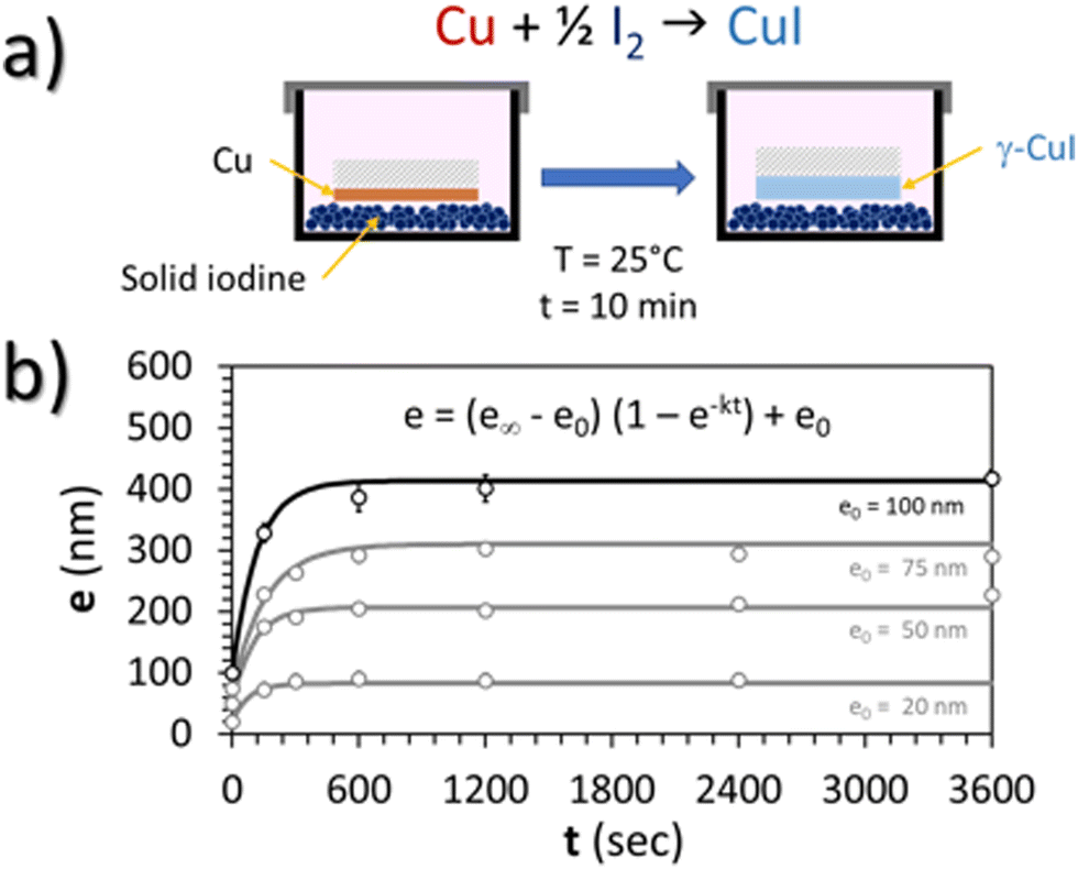 | ||
| Fig. 1 (a) Schematic solid iodation process. (b) Evolution of the thickness of the film (e) with the iodination time for various initial copper thicknesses (t0). Solid lines correspond to the proposed general kinetic law. | ||
As the Cu surface was directly placed facing iodine grains, some of the Cu atoms directly reacted with solid iodine crystals (Fig. 1(a)). Iodine vapor is also likely to react with the rest of the polycrystalline Cu thin films. Finally, the resulting CuI thin films were cleaned of any remaining I2 with pressurized air.
Thin film structural characterization was performed by X-Ray Diffraction (XRD) with a Bragg–Brentano geometry at ambient temperature using a Bruker D4 Endeavor diffractometer equipped with a Cu anode and a LynxEye 2D detector. Grazing incidence X-Ray Diffraction (GI-XRD) was also performed at room temperature. XRD and GI-XRD were also carried out at various temperatures using a Bruker D8 Advance diffractometer equipped with a Cu anode and an Anton Parr HTK1200N high-temperature chamber under inert gas or air. For the measurement under nitrogen, the acquisition was performed between 30 and 310 °C, under isothermal conditions with increments of 30 °C. Under air, the measurement was stopped at 200 °C due to oxidation. XRD and GI-XRD data were analyzed with the Bruker-EVA software using the JC-PDF database and refined with the Rietveld method38 implemented in the FullProf-Suite program.39
The composition of the thin films was characterized with a CAMECA SXFiveFE Field Emission Gun Electron Probe Micro Analyser (FEG-EPMA). For this specific measurement, the SiO2 glass substrate was replaced by a silicon wafer substrate in order to avoid the detection of oxygen due to the substrate. Measurements were carried out at various energies (7 and 15 keV) and processed by Cameca-LayerQuant software. AgI (99.999%, Alfa Aesar, CAS: 7783-96-2) and Cu (99.99%, Micro-Analysis Consultants Ltd, CAS: 7440-50-8) were used as internal standards for iodide and copper quantification. Additional pseudo-quantitative analyzes were carried out by X-Ray Fluorescence (XRF) using a Bruker S2 Ranger apparatus.
Microstructure was characterized with a JEOL JSM7800F Field Emission Gun Scanning Electron Microscope (FEG-SEM) and with a Nanoscope III Dimension 3000 Atomic Force Microscope (AFM). All AFM images were analyzed with the Gwyddion software.
The characterization of the transport properties was performed versus temperature using two probes and a thermal controller. The setup is composed of an interfaced Linkham cell (HFS600E-PB4 PROBE STAGE) equipped with a temperature controller, a Keithley 2400 source meter, a mass flow controller and electro valves. The measurements were performed on a 12 × 12 mm sample. Two platinum electrodes (12 × 2 mm) were deposited on the thin films with a spacing of 8 mm to neglect contact resistances. The electrical conductivity σ is therefore calculated by dividing the Pt electrodes spacing by the product of the CuI thin film section (which is the sample length multiplied by the thin film thickness) by the measured resistance. V(I) linearity was checked.
Hall measurement was performed at room temperature using the Van der Pauw method with an applied external magnetic field of 0.51 T.
The Seebeck coefficient was determined with a home-made measurement setup already described in other studies,40 with two independent heaters adapted to the thin film geometry. A thermal gradient was applied along the thin film. Verification of the temperature was made possible by using two carbon spots (emissivity of 0.97) deposited on the thin film with a carbon solution sprayed through a mask and an infrared camera which gave an accurate measure of the surface temperature of the thin film. The potential was measured using a Keithley 2182A Nanovoltmeter.
The optical transmittance and reflectance were measured using a Bentham PVE300 integrated spectrophotometer (Bentham Instruments Ltd, Berkshire, UK) in the 300 to 1100 nm wavelength range.
Results and discussion
Structure, microstructure, and composition of the Cu and γ-CuI thin films
The Cu thin film precursor and CuI thin film final product were both characterized by XRD, EPMA, SEM and AFM techniques.For the Cu thin film precursor, only the Cu metallic phase is visible from XRD (Fig. 2(c)) measurements confirming the effectiveness of the pre-deposition cleaning cycles. The microstructure of the Cu thin film, visible on the FEG-SEM images (Fig. 2(b)), is composed of spherical and monodisperse particles of about 20 nm in diameter from the surface view, and columns reaching the highest value of 100 nm with a dense layer of 25 ± 5 nm at the interface with the substrate from the cross section. Determined by a threshold measurement done with Gwyddion software over a field 1.5 μm wide, i.e. over around 80 columns, the average value of the column heights was determined at 60 nm. The AFM image of the top surface of Cu (Fig. 2(a)) shows a homogeneous layer of spherical particles with a diameter of 25 ± 5 nm in agreement with the FEG-SEM surface view.
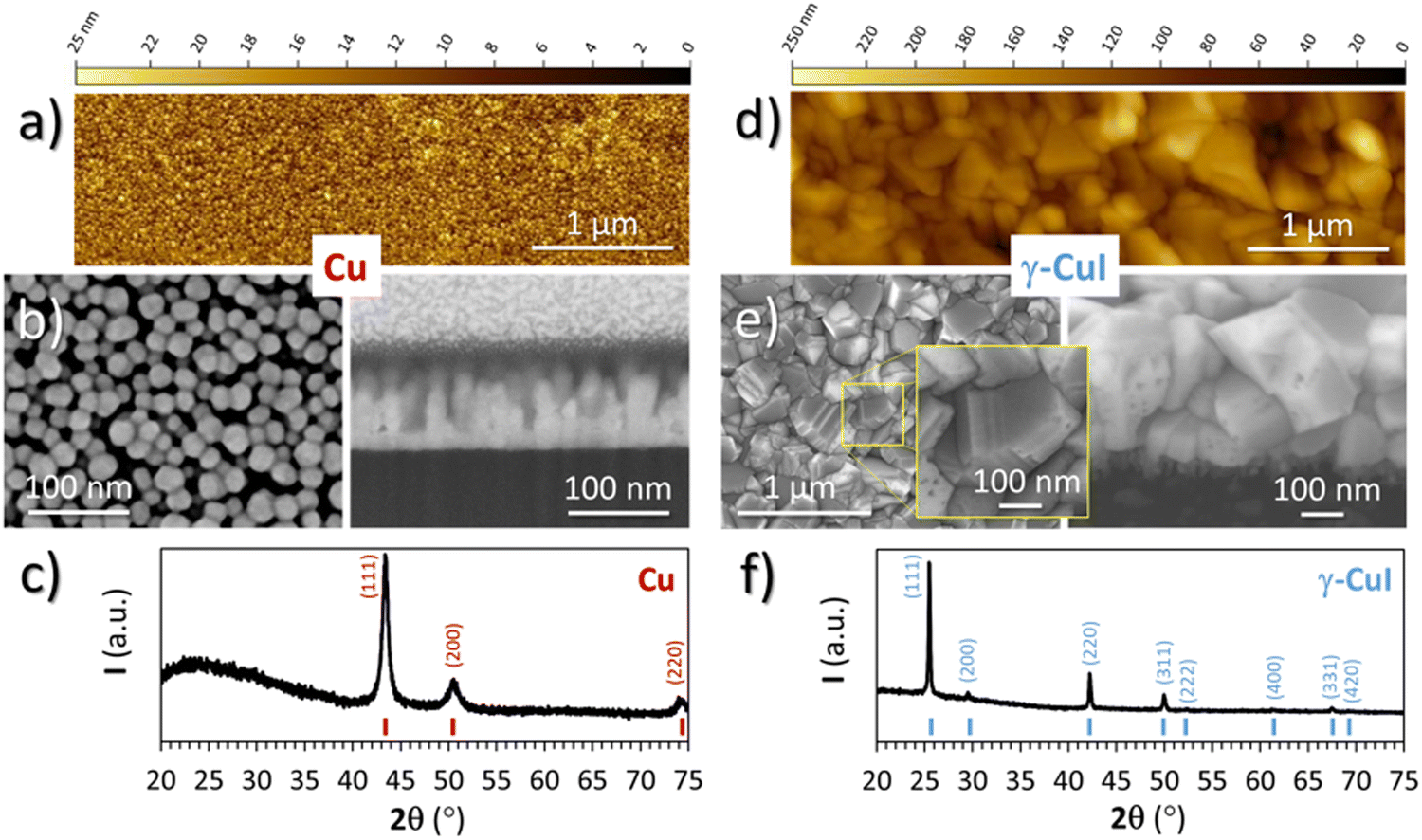 | ||
| Fig. 2 AFM planar view, FEG-SEM planar and cross section views and XRD pattern of (a)–(c) a Cu thin film precursor and (d)–(f) the γ-CuI thin film product. | ||
For the CuI thin film product, the XRD pattern (Fig. 2(f)) only shows the characteristic diffraction peaks of the γ-CuI phase (F3m with a = 6.0515(4) Å). The EPMA analyses indicate a composition of 49.2 at% for I and 50.2 at% for Cu. The rest corresponds to 0.6 at% of O. From these values, the atomic I/Cu ratio is equal to 0.98, i.e. very close to complete iodination. The evolution of the ratio of the Cu Kα measured at 20 kV over the I Lα measured at 20 kV was monitored by XRF over time for samples deposited on a silicon wafer substrate. After nine months, there is no significant evolution of the ratio Cu/I, which indicates no loss of iodine of the γ-CuI thin film over this period. A loss of iodine in γ-CuI thin films has been observed as early as five weeks after production,34 which contrasts with the stability of our thin film. The low final oxygen content as well as the purity of the γ-CuI phase demonstrates the initial purity of the Cu thin film.
FEG-SEM (Fig. 2(e)) and AFM (Fig. 2(d)) images of the γ-CuI surface show faceted crystals of a few hundred nanometers with different surface shapes, suggesting random orientations of the crystallites in agreement with the XRD. Domains separated by straight and parallel lines are clearly visible on the larger crystals by FEG-SEM (see the inset in Fig. 2(e)). These straight lines which correspond to twinning domains have already been observed by other authors41,42 and characterized recently by transmission electron microscopy at the temperature of liquid nitrogen.43
From the FEG-SEM cross-section view (Fig. 2(e)), the γ-CuI thin film total thickness is around 325 nm and its microstructure can be divided into two layers. The top layer, which is 300 nm thick, consists of large crystals with sizes between 100 and 300 nm, equivalent to those seen in the surface view. Very little intergranular porosity is observed, but a few holes can be detected on the surface of some crystals, certainly linked to point defects. The bottom layer located at the interface with the substrate is composed of smaller crystals of about 25 nm with large porosity. This microstructure is similar to what can be found in the literature.9,44,45
If we calculate the theoretical thickness of the γ-CuI layer from the thickness of the nominal copper layer (using the average thickness of 60 nm and the 100 nm maximum height of the column) and the respective molar volumes of the Cu and γ-CuI phases (Vm(Cu) = 7.1 cm3 mol−1 and Vm(γ-CuI) = 33.2 cm3 mol−1) which gives a ratio of 4.68, and we obtain a large range of theoretical thickness of 281–468 nm in agreement with that observed by SEM (325 nm). This suggests that the γ-CuI thin film is completely formed, in adequation with the stoichiometry found by EPMA and the final thicknesses of the films. This also makes sense with the high densification of the γ-CuI crystals observed in the FEG-SEM cross-section and surface view but also with the difference in microstructure observed in between the first 100 nm (constrained growth) and the rest of the γ-CuI layer (free growth).
Thermal stability of γ-CuI in air
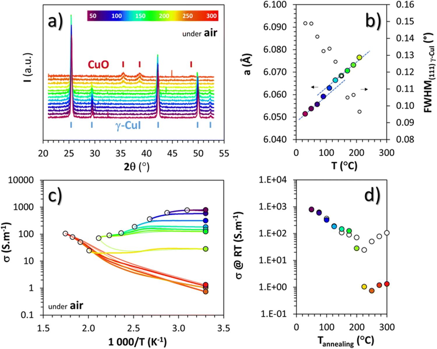
To study γ-CuI stabilization, it is first necessary to know its limitations in terms of temperature under air to determine the working temperature range. Fig. 3(a) shows the XRD patterns of the γ-CuI thin film with heat treatment under air, from 30 to 270 °C. Between 30 and 210 °C, only the characteristic Bragg peaks of the γ-CuI phase are present. From 210 °C, CuO tenorite is detected. The refined lattice parameter a of the γ-CuI phase is plotted versus annealing temperature in Fig. 3(b). Apart from a slight irregularity around 120 °C which can be attributed to a possible insertion of oxygen ( or
or  ) into the structure and which will be discussed later, a regular increase of the lattice parameter due to thermal expansion is observed to reach a = 6.0765(4) Å at 210 °C. This allows us to calculate the coefficient of linear expansion of the γ-CuI phase in air equal to α = 25 × 10−6 K−1. This linear expansion coefficient is almost similar to those reported under vacuum and/or Ar equal to α = 19–29 10−6 K−1.27–29,46 C. Moditswe et al. observed a small decrease of the lattice parameter in thin films with an increase in temperature during air annealing up to 200 °C, explained by a decrease of the tensile strain of the film, which is not observed in our case.30 Less than 0.15% of microstrains are found in a pristine thin film from an analysis of the Full Width at Half Maximum (FWHM) based on the Williamson & Hall's plot.47 A linear decrease of the FWHM of the Bragg's peak (111) noted a FWHM(111) from 0.15 to 0.09° is found during the annealing treatment from 50 to 210 °C (Fig. 3(b)). Considering the instrumental contribution and the limited microstrain, the decrease in the FWHM is attributed to an increase of the apparent crystallite size from 140 to 280 nm as estimated by the Debye & Scherrer equation.48 These values are consistent with the overall thickness and the grain microstructure of the pristine thin film observed by FEG-SEM (Fig. 2(b)).
 | ||
| Fig. 3 Thermal treatment of the γ-CuI thin film under air with: (a) HT-XRD patterns up to 300 °C; (b) refined lattice parameter a and FWHM(111) of the γ-CuI phase during warming up to 210 °C; (c) cycled conductivity measurement from 50 to 300 °C by 25 °C steps; (d) conductivities at room temperature after each annealing step σRT (in color) and conductivities at maximum annealing temperature σT extracted from (c) over the Tmax annealing. | ||
Electrical measurements were also carried out under air between 50 and 300 °C every 25 °C steps, with each time a return to 30 °C between the steps. The changes in electrical conductivity (σ) as a function of temperature as well as the conductivity values measured at room temperature (σRT) between each step are represented by white and colored circles respectively in Fig. 3(c) and (d). Up to 200 °C, i.e. for the pure γ-CuI phase, σRT decreases after each increasing temperature cycle. This decrease is particularly visible up to 120 °C, then from 120 °C to 200 °C, the hysteresis becomes small, a sign of stabilization of the transport properties at around 150 S m−1. Above 200 °C, the phase transition from γ-CuI to CuO previously highlighted with X-rays is clearly visible through the significant change of the ln![[thin space (1/6-em)]](https://www.rsc.org/images/entities/char_2009.gif) σ = f (1000/T) slope in Fig. 3(c) (as well as in between σT and σRT in Fig. 3(d)). This corresponds to a transition from degenerated to semiconducting behavior. The negative slope obtained for CuO corresponds to a transport activation energy (Ea) of 0.18 eV, similar to those previously reported for CuO films.49
σ = f (1000/T) slope in Fig. 3(c) (as well as in between σT and σRT in Fig. 3(d)). This corresponds to a transition from degenerated to semiconducting behavior. The negative slope obtained for CuO corresponds to a transport activation energy (Ea) of 0.18 eV, similar to those previously reported for CuO films.49
Both structural and electrical characterization of the thermal stability under air of the γ-CuI phase show a phase transition toward CuO between 200 and 220 °C, limiting the use of CuI exposed to air for temperature ranges above 200 °C.
Thermal stability of γ-CuI in a neutral atmosphere
To avoid the oxidation of γ-CuI into CuO, and therefore potentially extending the stability range of γ-CuI, heat treatments in a neutral atmosphere were also carried out.Temperature XRD patterns of the γ-CuI thin films under nitrogen, from 30 to 390 °C in 20 °C steps are shown in Fig. 4(a). Up to 350 °C, the γ-CuI structure is stable. From 370 °C, characteristic Bragg's peaks of the rhombohedral β-CuI are observed in agreement with previous studies.24–27 The γ-CuI refined lattice parameter a and FWHM(111) are plotted in Fig. 4(b) for a second sample annealed only up to 300 °C to keep the γ-CuI phase unchanged and to prevent any excessive increase in the disorder of the Cu+ ion sub-lattice close to the transition toward β-CuI.27 A reproducible increase and decrease of the lattice parameter during warming and cooling was then observed (a = 6.0766(6) Å at 200 °C and a = 6.0926(5) Å at 300 °C) and leads to a coefficient of linear expansion of the γ-CuI phase of α = 27 × 10−6 K−1, almost identical to that found during the treatment under air. One can notice the absence of irregularity in the lattice parameter under a neutral atmosphere at around 120 °C in opposition to what had been observed under air (cf.Fig. 3(b)), and which supports the hypothesis of an effect of oxygen during the air treatment. Concomitantly, a constant decrease of the FWHM(111) is observed during warming reaching 0.09° at 300 °C. This value remains constant during cooling back down to 50 °C (Fig. 4(b)). It corresponds to an irreversible modification of the apparent crystallite size which is stabilized to 280 nm by the Debye & Scherrer equation.
 | ||
| Fig. 4 Thermal treatment of the γ-CuI thin film under a neutral atmosphere with: (a) HT-XRD patterns under nitrogen up to 390 °C; (b) refined lattice parameter a and FWHM(111) of the γ-CuI phase during warming up to 300 °C (circle) and cooling (diamond); (d) 2 successive cycled conductivity measurements from 50 to 300 °C by 25 °C steps; (c) conductivities at room temperature after each annealing step σRT (in color) and conductivities at maximum annealing temperature σT extracted from (c) for the 2 cycles over the Tmax annealing. | ||
As for the air treatment, electrical measurements were carried out under argon between 50 and 300 °C every 25 °C step, with each time a return to 30 °C between the steps. The changes in electrical conductivity (σ) as a function of temperature as well as the conductivity values measured at room temperature (σRT) between each step are represented by white and colored circles respectively in Fig. 4(c) and (d). After any heat treatment over 50 °C, the conductivity of the thin film evolves irreversibly. The conductivity at the maximum temperature of the annealing step (σT represented with white circles) decreases constantly during heating up to 200 °C. Beyond 200 °C, σT stabilizes below ≈10 S m−1 which is much lower than the value obtained under air. During warming, a slight change in the conductivity at around 220 to 240 °C is noticed but not yet explained. For all of these temperature steps, cooling did not change the conductivity values as shown with an approximate superposition of σT and σRT represented by the white and colored circles respectively in Fig. 4(d).
Optimized transport properties of γ-CuI
Because the oxygen present in cuprous iodide can greatly increase the electrical conductivity of this material,50 once stabilized at 300 °C under argon, the thin film of γ-CuI was then annealed at 150 °C under synthetic air.From the structural and microstructural point of view, any changes were denoted from the pristine material (Fig. 2) and the annealed one (Fig. 5). The lattice constant determined by XRD (not shown here) is almost unchanged with a = 6.0502(3) Å as well as crystallite sizes (200 ± 80 nm extracted from the AFM images (Fig. 5(d)) and a coherent length of 280 nm by XRD). The RMS roughness (Rq) of the thin film slightly increases with the thermal treatment from 21 nm to 28 nm. As shown on the surface and perspective FEG-SEM and AFM images (Fig. 5(a)–(c)), faceted crystals of a few hundred nanometers with different surface shapes are still present.
 | ||
| Fig. 5 Thermal treatment of the stabilized γ-CuI thin film under dry synthetic air with: (a)–(c) FEG-SEM planar and cross section views for various magnification; (d) AFM planar view; (e) cycled conductivity measurements from 50 to 150 °C by 25 °C steps then back to 50 °C; (f) conductivities at room temperature after each annealing step σRT (in color) and conductivities at maximum annealing temperature σT extracted from (e) over the Tmax annealing for warming and cooling. | ||
The microstructure is also still made of large crystals with sizes between 100 to 300 nm on the top layer and smaller crystals of about 60 nm on the bottom layer (Fig. 5(c)). The total thickness is still close to 400 nm. More and wider porosities are now visible as well as a softening of the edges of the large crystals. Straight and parallel lines due to twinning domains are less visible than in Fig. 2(b), a sign of the decrease of plane defects with the annealing treatment.
EPMA analyses of the γ-CuI thin film that was annealed under argon at 300 °C then under synthetic air at 150 °C were carried out under the same conditions as for the pristine γ-CuI thin film. With 48.2 at% for I and 49.5 at% for Cu, the I/Cu ratio remains almost constant at 0.97 (0.98 for the pristine γ-CuI thin film). With 2.3 at% for O (against 0.6 at% for the pristine film), a significant increase of the oxygen content is denoted, proof of the diffusion of oxygen into the film. XRF monitoring of the stabilized and optimized γ-CuI thin films showed that the Cu/I ratio is stable over time. The Cu/I ratio tends to increase over nine months, but this increase is still within the margin of error.
The electric behavior of the γ-CuI thin film thermally treated under synthetic dry air up to 150 °C directly after the stabilization treatment under argon, with each time a return to 30 °C between the steps is shown in Fig. 5(e). The changes in electrical conductivity (σ) as a function of temperature as well as the conductivity values measured at room temperature (σRT) between each step are again represented by white and colored circles respectively in Fig. 5(e) and (f). The scales of the axes are kept constant in order to be able to directly compare the results with the previous heat treatments shown in Fig. 3 and 4. First, the results show an increase of the conductivity with an annealing temperature of only 50 °C. This conductivity continues to increase until reaching a stable value of around 150 S m−1 between 100 and 125 °C, and did not further evolve up to 150 °C. Even after a second series of annealing from 50 to 150 °C, the conductivities measured at 30 °C remained stable at 152 S m−1.
According to the structural and microstructural observations, the variations in the electrical properties cannot be attributed to a change in microstructure as Ar treatment was previously applied at higher temperatures and allowed for the stabilization of the microstructure. The increase of the electrical conductivity could only be due to the doping by absorption of oxygen according to previous works which report that oxygen traces can act as an electron trap by inserting itself into iodine vacancies (VI) leading to the formation of ( ) defects which correspond to a p-type doping.11,31 It is also possible to have oxygen in an interstitial (
 ) which is also considered as a p type defect.
Relationships between the structure/defects and properties
All expected point defects which should be present in our γ-CuI thin films are listed in Fig. 6(a). They correspond to intrinsic iodine and copper Frenkel-defects, the Schottky defect, as well as n- and p-intrinsic defects. Due to the impact of oxygen, two additional extrinsic defects are also reported. | ||
| Fig. 6 (a) Representation of the Blend zinc γ-CuI structure and the various p-type (in blue) and n-type (in grey) defects (intrinsic and extrinsic defects in the case of the presence of oxygen atoms in the structure) and ambivalent Frenkel and Schottky defects. Iodine atoms are represented in green and copper in orange. The radius of the atoms is taken into consideration in the structural representation. (b) The evolution of defects with thermal treatment as a function of atmosphere explains the electrical conductivity behavior. | ||
Among the above listed point defects, some have a low probability of existing, such as p-type  or
or  , due to a high defect formation energy and the steric effect of iodine. Other defects, including single
  , should be difficult to obtain in Cu-rich conditions even if their formation energy is lower in comparison with other intrinsic defects (
 ,
,  and
and  ,
,  ,
,  ).14 However,
  could still exist in our pristine sample within Schottky and Cu–Frenkel pair defects, i.e. just after the iodination process and without any heat treatment applied to rearrange the atom in the structure. In this case, the n-type
  counter defects (issued from Schottky and/or I–Frenkel pair defects) could be transformed into p-type
  due to the oxygen in air (
 ) as the radius of the oxygen (138 pm according to R. D. Shannon51) is lower than iodine (202 pm calculated from lattice parameter and Cu+ ionic radii in coordination IV). This hypothesis is possible as mentioned in previous reports whereas oxygen traces can act as an electron trap in γ-CuI films by inserting itself into iodine vacancies (
 ) and leading to the formation of (
 ) defects which correspond to p-type doping.11,30 N-type defects
  issued from the initial Cu-Frenkel defects could also be present in our samples. Even if these defects exist, they would not impact the electrical conductivity which is mainly led by
  and
and  for the hole conductivity and as the
  is located deeper in the forbidden band. As a result, we can assume that only p-type defects such as
  (generated by initial Schottky and/or I–Frenkel pair defects) and extrinsic
  are initially present and active in our pristine γ-CuI films. This is supported by a p-type degenerated semiconductor behavior (a higher electrical conductivity) and the EPMA analysis which has revealed the presence of oxygen in the films.
During the first thermal treatment under air, the electrical conductivity decreases after each temperature cycle until γ-CuI oxidizes into CuO. In the 30 to 120 °C temperature range, the decreasing of the electrical conductivity is strong and could be explained by the thermally activated structural rearrangement which contributes to minimizing the  defects according to
  . This structural reorganization will decrease the number of holes and the electrical conductivity as well. Above 120 °C, the decreasing of the electrical conductivity becomes slower and can be correlated to the small gap increase of the lattice parameter. This can be due to a possible oxygen insertion in the structure according to
  . This effect counterbalances the decreasing trend of the number of p-type defects. The global trend is also partially compensated by an irreversible microstructural evolution (i.e. increasing of the crystallite sizes with the thermal treatment which should increase the carrier mobility). Both contributions justify the non-linearity and the irreversibility of the electrical conductivity with temperature cycling. This agrees with the evolution of the decreasing number of point of defects with the temperature coupled to an evolution of the microstructure.
In the case of the Ar thermal treatment, it also removes the Schottky and Frenkel defects and tends to minimize the initial  and
and  defects (in opposition with treatment under air). In this case, the total number of defects becomes lower and the conductivity decreases until about only 10 S m−1. This is the lowest electrical conductivity of our γ-CuI films, in agreement with a low number of defects. The microstructural evolution (similar to the first air thermal treatment) is also present but cannot fully counterbalance the strong decreasing of electrical conductivity induced by the small number of defects.
Finally, when the Ar treatment is followed by an additional treatment under air, the variation of the electrical properties cannot be attributed to a change in microstructure as the films were already treated at higher temperature. Therefore, the increase of the electrical conductivity could only be due to the reinsertion of oxygen in the structure ( ,
,  ) which generates p-type defects and returns to the same state as the first treatment under air (σ = 152 S m−1 at room temperature). This step proves the existence of exchange with the oxygen in the γ-CuI. This result is consistent with the study reported by Inudo et al.16 which also showed that the electrical conductivity of γ-CuI films prepared by spin coating are lower in the case of neutral thermal treatments than in air thermal treatments (76 S m−1 instead of 330 S m−1).
We can conclude that oxygen has an important effect on the electrical conductivity in our γ-CuI thin films. Fig. 6(b) schematically summarizes the evolution of the defects with thermal treatment in air and in Ar in our γ-CuI films which can explain the evolution of electrical conductivity behavior. This work highlights that the conductivity at room temperature σRT therefore strongly depends on the thermal history of the sample (often unspecified in the literature), and in significant proportions since it is greater than two orders of magnitude. These irreversible changes in γ-CuI's electronic properties with respect to temperature result in an important limitation for the understanding of the intrinsic properties of this material and its commercialization. However, this work shows that pre-treatment at 300 °C under argon makes it possible to obtain reproducible properties.
Thermoelectric properties of stabilized γ-CuI
Measurement of the Seebeck coefficient (S) with respect to temperature under an air atmosphere up to 140 °C was carried out and is presented in Fig. 7 for the stabilized γ-CuI. Contrary to the as-deposited sample (measurement not shown here), no hysteresis is detected between the warming (circle) and the cooling (diamond) steps, which proves that the compound is stable even after being heated to 140 °C in agreement with the conductivity measurements. | ||
| Fig. 7 Seebeck coefficient S and power factor PF as a function of the temperature under air up to 140 °C during warming (circle) and cooling (diamond). The blue line is only a guide for the eye. | ||
The Seebeck measurement also confirmed the stability of the thermally treated γ-CuI thin films.
The Seebeck coefficient increases linearly with the temperature from S = 287 μV K−1 at 44 °C to S = 711 μV K−1 at 139 °C, which is a sign of a degenerated semiconductor behavior. According to the Mott formalism of degenerated semiconductors with acoustic lattice vibration scattering mode and a parabolic band approximation, the Fermi level (EF) position is given by 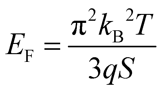 where kB is the Boltzmann constant, T is the temperature, q is the fundamental charge, and S is the Seebeck coefficient. In this case, the Fermi level is calculated from the Seebeck versus temperature slope and is equal to EF = −5.56 meV in the valence band (Ev arbitrary fixed at 0 eV).
According to J. Wang et al.,52 the band structure of the CuI consists of two valence bands for heavy and light holes respectively. The effective mass (m*) of heavy holes are 2.14 (2.4 experimentally according to B. Honerlage et al.53) and 0.3 for light holes. With these data, considering a parabolic band and our determined EF, the calculated hole concentrations are 7.26 × 1019 cm−3 (with mhh* = 2.4) and 3.37 × 1018 cm−3 (with mlh* = 0.30) for heavy holes and light holes respectively. With the relaxation time approximation (τhh = τlh), the calculated macroscopic hole mobilities are μhh = 0.15 cm2 V−1 s−1 and μlh = 1.24 cm2 V−1 s−1. These values agree with those reported by Yamada et al.17 and Inuda et al.16 for CuI thin films and are an extension of the mobilities determined by P. Storm et al.54 which have measured mobilities as a function of hole density.
Considering only the impact of the substrate (Ks = 0.8 W m−1 K−1) on the thermal gradient by approximation according to I. Sinnarasa et al.,55 an effective 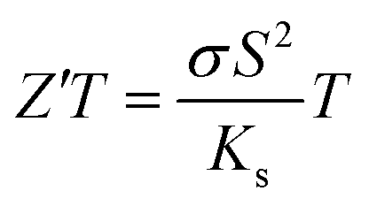 can be calculated for the stabilized γ-CuI: Z′T = 0.02 at 100 °C. This value is 2.6 time larger than previously reported p-type Mg doped CuCrO2 thin film at the same temperature.55
The carrier density (1019 cm−3), the large Seebeck coefficient and the Z′T from this work are clearly adapted for thermoelectric applications.56
Hall effect measurement
Hall measurements were performed on as-deposited, intermediate (Ar annealing) and stabilized (Ar + Air annealing) samples. All measurements report p-type behavior with a positive Hall resistance. The calculated hole densities are 2 × 1019 cm−3, 4 × 1017 cm−3 and 2 × 1018 cm−3 for as-deposited, intermediate and stabilized films respectively. This variation of hole density totally agrees with the evolution of defects with the thermal treatment as reported in Fig. 6 and previously discussed. In the case of the first treatment under Ar, the thermally activated structural rearrangement combined with the disappearance of the Schottky and Frenkel defects generates a clear reduction of the hole densities from 2 × 1019 cm−3 to 4 × 1017 cm−3. The final annealing treatment under air whereas the exchange with oxygen is quantified by EPMA clearly induce an increase of the hole densities from 4 × 1017 cm−3 to 2 × 1018 cm−3 in good agreement with the conductivity measurement.Even if it is reported in the literature that Hall measurement is better adapted to materials with single band conduction, high mobility and relatively low carrier density,57 the hole density determined from Hall measurement (pH) is compared to those obtained from Seebeck for the light holes (pSlh) and the heavy holes (pShh) for the stabilized sample. pH = 2 × 1018 cm−3 is comparable to pSlh = 3.37 × 1018 cm−3 while a real difference exists in between pH and pShh = 7.6 × 1019 cm−3. This observation can be explained if we consider the impact of light (RH-lh = 2.36 Ω) and heavy holes (RH-hh = 0.1 Ω) on the total Hall resistance by using the heavy and light holes density obtained from Seebeck measurement. RH-lh is greater more than 20 times compared with RH-hh which is in the range order of the experimental noise. Hall measurement is mainly sensitive to light hole density (with higher mobilities and lower density). The low gap between pH and pSlh could be explained by the measurement accuracies of each technique and the microstructural influence. Indeed, Hall measurement is microstructurally dependent and relates to the true current section which can be lower than the total thickness of the film, whereas Seebeck is an intrinsic characteristic of the material. For all these reasons, Hall measurement is not well adapted to measure the heavy holes contribution to the electrical conductivity and the impact of these heavy holes are often forgiven.
Optical properties of stabilized γ-CuI
Optical characterization parameters including the measured total transmittance (T), total reflectance (R), and the absorption coefficient α (α = 1/eln((1 − R)/T) with e = thickness) are presented in Fig. 8(a) and (c) respectively for the pristine and thermal treated (300 °C under argon followed by 150 °C under air) γ-CuI thin films.
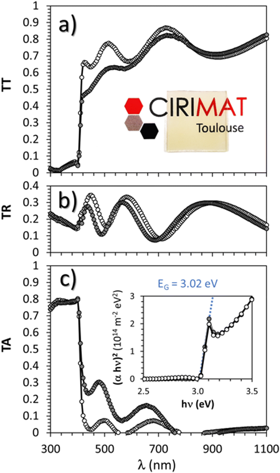 | ||
| Fig. 8 Optical properties of γ-CuI thin films before (grey line) and after (black line) thermal treatment at 300 °C under Ar followed by 150 °C under synthetic air: (a) total transmittance TT and a picture of the Ar and Air treated film; (b) total reflectance TR; (c) absorption coefficient α and Tauc plots for the direct optical bandgap determination. | ||
The average total transmittance, within the wavelength visible region 400 nm to 800 nm, are equal to 72% and 65% respectively for both samples. They are close to the common values found in the literature9,13,43,58 Except for small interference effects due to layer thickness variations (which permit to determine a thickness of around 310 nm by optical simulation close to the 325 nm obtained by FEG-SEM), γ-CuI thin film total reflectance did not vary significantly with the thermal treatment between 16% and 17% on average. The strong absorption observed at around 400 nm corresponds to the EG optical bandgap. The Tauc plots (inset Fig. 8(c)) show an invariable direct band gap of about EG = 3.02 eV for both pristine and annealed γ-CuI thin films. The determined direct EG is also in agreement with experimental59–61 and theoretical values.14 A tiny absorption peak is visible at 400 nm (3.1 eV), close to the absorption edge on the absorption spectra (Fig. 8(c)) as well as on the transmission spectra (Fig. 8(a)). This singularity is often observed in γ-CuI whatever the synthesis process (atomization,33 SILAR,61 liquid-phase iodation60). The absorption edge at 411 nm (3.02 eV) is due to a direct transition with two types of exitonic transitions (first for heavy holes and a second one for light holes) while the other absorption edge (3.68 eV) is due to a spin orbit contribution according to P. Storm et al.54
Figure of merit
To evaluate the performance of optical and electrical properties, transparent conducting materials are often characterized by their figure of merit (FOM). The most used FOMs were proposed by D. B. Fraser and H. D. Cook (T/Rs),62 G. Haacke (T10/Rs or even (T/n√Rs)),63,64 or R. Gordon (σ/α = −1/(RslnT))65 where in all cases, T is the mean total transmittance and Rs is the sheet resistance. In this work, for the stabilized and optimized γ-CuI thin film T = 65% and Rs = 2 × 10⁴ Ω, resulting in a Haacke's FOM equal to 6.7 × 10⁻⁷ Ω−1. This FOM is similar to that of other p-type TCO materials,4,66,67 and similar58 or even lower13,59,68 than that of other γ-CuI thin films. This difference can be explained by the fact that, in this work, the thin films were not prepared in an iodine rich environment, causing a limited number of Cu vacancies which is beneficial for p-type electrical conduction. Most importantly, this difference can be explained by the thermal process used in our work to stabilize the electrical properties of the γ-CuI thin film. If we consider the as-deposited film where σ = 792 S cm−1 and TT = 72%, Haacke's FOM reaches 9.6 × 10⁻⁴ Ω−1. Even if this FOM is close to the highest values reported in the literature for this kind of material so far, this work highlights that this value has only little interest for an application requiring the use of temperature.
Equivalent to the coupled evaluation of the optical and electronic properties of TCO by different figure of merit formulations, a power factor (PF) defined as PF = σS2 where σ is the electrical conductivity and S is the Seebeck coefficient, is also often used to evaluate the thermoelectric performance of materials. PF is often expressed in μV2 Ω−1 cm−1 K−2, i.e. μW m−1 K−2 homogeneous with kg m K−2 s−3 in the international unit system. With σ = 152 S m−1 and S = 287 μV K−1, a PF = 12 μW m−1 K2 is obtained in this work at ≈40 °C. A reversible increase of the power factor with the temperature which makes it possible to reach 66 μW m−1 K−1 at ≈130 °C, certainly represents modest thermoelectric performances for thin films, but reveals a good stability of the material and justifies the stabilization treatment to be able to use the γ-CuI material under good conditions.
Due to its transparency and its thermoelectric performances, γ-CuI presents a real interest as a transparent thermoelectric thin film. Thereby, we propose for the first time a transparent thermoelectric Coefficient of Performance (COPTTE) which both integrates the thermoelectric power factor and the transparent conducting figure of merit (Haacke): COPTTE = PF × FOMHaacke which can be calculated by: COPTTE = (T10S2)/(Rs2e) = T10S2σ2e where T is the mean total transmittance, S is the Seebeck coefficient, Rs is the sheet resistance, σ is the electrical conductivity, and e is the thickness of the thin film. COPTTE will be homogeneous to A2 m−1 K−2. A larger value of COPTTE indicates better performances of the material in both TC and TE properties. This COPTTE value can now be used as a reference value in the evaluation of transparent thermoelectric thin films. In this work, with T = 65%, S = 287 μV K−1 and σ = 152 S m−1, the COPTTE for the stabilized γ-CuI thin films, COPTTE is equal to 8.3 × 10⁻¹² A2 m−1 K−2.
As this COPTTE factor is a new factor of merit, it seems interesting to position the performances obtained in this work in relation to those obtained by other authors. The values of transmittance, Seebeck coefficient and conductivities found in the literature, as well as the FOM, PF and COPTTE calculated by the authors from the compiled data, are listed in Table 1 for γ-CuI and also for other thin film materials (Delafossite, other oxides, oxy-chalcogenide) that exhibit p-type conductivity. Graphical representation of power factor and Haacke's FOM for these p-type thin film materials is shown in Fig. 9. Despite the large number of references on p-type TCO materials, a limited COPTTE could be calculated due to insufficient corresponding thermoelectric data (and vice versa).
| Thin film composition | Ref. | Deposition technique | e (nm) | T (%) | R s (Ω) | σ (S m−1) | FOMHaacke (Ω−1) | S (μV K−1) | PF (μW m−1 K2) | COPTTE (A2 m−1 K−2) |
|---|---|---|---|---|---|---|---|---|---|---|
| a The thickness of the films is not given precisely in the reference but only typical values of 100–300 nm. An average thickness of 200 nm is then taken for calculation. | ||||||||||
| SrCu2O2:K | 69 | PLD | 120 | 80 | 1.74 × 10⁶ | 4.8 × 10 | 6.18 × 10⁻⁸ | 260 | 3.24 × 10⁻¹ | 2.0 × 10⁻¹⁴ |
| CuAlO2 | 70 | PLD | 500 | 70 | 2.11 × 10⁴ | 9.5 × 10 | 1.34 × 10⁻⁶ | 183 | 3.18 × 10 | 4.3 × 10⁻¹² |
| CuGaO2 | 70 | PLD | 500 | 80 | 3.17 × 10⁵ | 6.3 × 10 | 3.38 × 10⁻⁷ | 560 | 1.98 × 10 | 6.7 × 10⁻¹³ |
| CuAlO2 | 71 | PLD | 230 | 70 | 1.28 × 10⁵ | 3.4 × 10 | 2.21 × 10⁻⁷ | 214 | 1.56 × 10 | 3.4 × 10⁻¹³ |
| LaCuOS | 72 | RF Sputtering | 200 | 70 | 4.17 × 10⁶ | 1.2 × 10 | 6.78 × 10⁻⁹ | 150 | 2.70 × 10⁻² | 1.8 × 10⁻¹⁶ |
| LaSrCuOS | 72 | RF Sputtering | 130 | 70 | 2.96 × 10⁵ | 2.6 × 10 | 9.55 × 10⁻⁸ | 40 | 4.16 × 10⁻² | 4.0 × 10⁻¹⁵ |
| CuCrO2:Mg | 73 | RF Sputtering | 270 | 30 | 3.70 × 10² | 1.0 × 10⁴ | 1.59 × 10⁻⁸ | 150 | 2.25 × 10² | 3.6 × 10⁻¹² |
| CuCrO2:Mg | 73 | RF Sputtering | 270 | 40 | 3.70 × 10⁴ | 1.0 × 10² | 2.83 × 10⁻⁹ | 150 | 2.25 × 10 | 6.4 × 10⁻¹⁵ |
| CuInO2:Ca | 74 | PLD | 100 | 40 | 3.57 × 10⁷ | 2.8 × 10⁻¹ | 2.94 × 10⁻¹² | 480 | 6.45 × 10⁻² | 1.9 × 10⁻¹⁹ |
| CuYO2:Ca | 75 | Thermal Co-Evap. | 240 | 40 | 4.00 × 10⁴ | 1.0 × 10² | 2.62 × 10⁻⁹ | 275 | 7.56 × 10 | 2.0 × 10⁻¹⁴ |
| La/SrCuOS | 76 | RF Sputtering | 150 | 60 | 3.33 × 10³ | 2.0 × 10³ | 1.81 × 10⁻⁶ | 44 | 3.87 × 10 | 7.0 × 10⁻¹² |
| LaCuOS | 76 | RF Sputtering | 150 | 60 | 1.04 × 10⁹ | 6.4 × 10⁻³ | 5.80 × 10⁻¹² | 713 | 3.25 × 10⁻³ | 1.9 × 10⁻²⁰ |
| CuBO2 | 77 | PLD | 200 | 75 | 3.03 × 10⁴ | 1.7 × 10² | 1.86 × 10⁻⁶ | 7 | 8.09 × 10⁻³ | 1.5 × 10⁻¹⁴ |
| ZnCo2O4 | 78 | PLD | 200a | 26.1 | 8.20 × 10⁴ | 6.1 × 10 | 1.79 × 10⁻¹¹ | 131 | 1.05 × 10 | 1.9 × 10⁻¹⁷ |
| ZnIr2O4 | 78 | PLD | 200a | 60.8 | 2.39 × 10⁴ | 2.1 × 10² | 2.89 × 10⁻⁷ | 54 | 6.07 × 10⁻¹ | 1.8 × 10⁻¹³ |
| ZnRh2O4 | 78 | PLD | 200a | 54.8 | 1.77 × 10⁴ | 2.8 × 10² | 1.38 × 10⁻⁷ | 63 | 1.14 × 10 | 1.6 × 10⁻¹³ |
| CuCrO2:Mg | 79 | Spray Pyrolysis | 155 | 85 | 3.23 × 10⁵ | 2.0 × 10 | 6.10 × 10⁻⁷ | 90 | 1.62 × 10⁻¹ | 9.9 × 10⁻¹⁴ |
| CuCrO2:Mg | 79 | Spray Pyrolysis | 305 | 70 | 3.28 × 10⁴ | 1.0 × 10² | 8.62 × 10⁻⁷ | 70 | 4.90 × 10⁻¹ | 4.2 × 10⁻¹³ |
| CuAl0.5Cr0.5O2 | 80 | Dip Coating | 315 | 39 | 4.44 × 10⁵ | 7.1 × 10 | 1.83 × 10⁻¹⁰ | 159 | 1.81 × 10⁻¹ | 3.3 × 10⁻¹⁷ |
| CuCrO2 | 80 | Dip Coating | 200 | 32 | 1.05 × 10⁷ | 4.8 × 10⁻¹ | 1.07 × 10⁻¹² | 290 | 4.00 × 10⁻² | 4.3 × 10⁻²⁰ |
| CuAlO2 | 81 | Dip Coating | 530 | 65 | 1.32 × 10⁷ | 1.4 × 10⁻¹ | 1.02 × 10⁻⁹ | 440 | 2.77 × 10⁻² | 2.8 × 10⁻¹⁷ |
| CuCrO2 | 81 | Dip Coating | 280 | 32 | 2.14 × 10⁶ | 1.7 × 10 | 5.25 × 10⁻¹² | 202 | 6.80 × 10⁻² | 3.6 × 10⁻¹⁹ |
| CuCrO2 | 82 | Spin Coating | 103 | 75 | 5.28 × 10⁶ | 1.8 × 10 | 1.07 × 10⁻⁸ | 266 | 1.30 × 10⁻¹ | 1.4 × 10⁻¹⁵ |
| CuCrO2:Mg | 82 | Spin Coating | 107 | 68 | 3.40 × 10⁶ | 2.7 × 10 | 6.21 × 10⁻⁹ | 202 | 1.12 × 10⁻¹ | 7.0 × 10⁻¹⁶ |
| CuCrO2:Mg | 82 | Spin Coating | 113 | 66 | 6.50 × 10⁵ | 1.4 × 10 | 2.41 × 10⁻⁸ | 180 | 4.41 × 10⁻¹ | 1.1 × 10⁻¹⁴ |
| CuCrO2:Mg | 82 | Spin Coating | 105 | 65 | 4.84 × 10⁶ | 2.0 × 10 | 2.78 × 10⁻⁹ | 248 | 1.21 × 10⁻¹ | 3.4 × 10⁻¹⁶ |
| Cr2O3:Mg,N | 83 | Spray Pyrolysis | 150 | 65 | 6.69 × 10⁴ | 1.0 × 10² | 2.01 × 10⁻⁷ | 70 | 4.88 × 10⁻¹ | 9.8 × 10⁻¹⁴ |
| CuCrO2 | 84 | Spin Coating | 125 | 66 | 2.96 × 10⁶ | 2.7 × 10 | 5.29 × 10⁻⁹ | 230 | 1.43 × 10⁻¹ | 7.6 × 10⁻¹⁶ |
| CuInO2 | 85 | Reactive Evap. | 120 | 65 | 7.31 × 10² | 1.1 × 10⁴ | 1.84 × 10⁻⁵ | 20 | 4.56 × 10 | 8.4 × 10⁻¹¹ |
| CuInO2 | 85 | Reactive Evap. | 120 | 65 | 6.67 × 10² | 1.3 × 10⁴ | 2.02 × 10⁻⁵ | 20 | 5.00 × 10 | 1.0 × 10⁻¹⁰ |
| CuCrO2:Mg | 86 | RF Sputtering | 300 | 40.7 | 1.67 × 10⁷ | 2.0 × 10⁻¹ | 7.48 × 10⁻¹² | 804 | 1.29 × 10⁻¹ | 9.7 × 10⁻¹⁹ |
| CuCrO2:Mg | 86 | RF Sputtering | 100 | 63.3 | 7.14 × 10⁴ | 1.4 × 10² | 1.45 × 10⁻⁷ | 114 | 1.82 × 10 | 2.6 × 10⁻¹³ |
| CuCrO2:Mg | 86 | RF Sputtering | 300 | 40.7 | 6.31 × 10² | 5.3 × 10³ | 1.98 × 10⁻⁷ | 121 | 7.73 × 10 | 1.5 × 10⁻¹¹ |
| La/SrCrO3 | 87 | MBE | 100 | 66.9 | 8.33 × 10⁴ | 1.2 × 10² | 2.15 × 10⁻⁷ | 321 | 1.24 × 10 | 2.7 × 10⁻¹² |
| La/SrCrO3 | 87 | MBE | 67 | 63.4 | 4.15 × 10⁴ | 3.6 × 10² | 2.53 × 10⁻⁷ | 281 | 2.84 × 10 | 7.2 × 10⁻¹² |
| La/SrCrO3 | 87 | MBE | 80 | 54.2 | 8.33 × 10³ | 1.5 × 10³ | 2.63 × 10⁻⁷ | 180 | 4.86 × 10 | 1.3 × 10⁻¹¹ |
| La/SrCrO3 | 87 | MBE | 50 | 42.3 | 3.70 × 10³ | 5.4 × 10³ | 4.95 × 10⁻⁸ | 80 | 3.46 × 10 | 1.7 × 10⁻¹² |
| CuCrO2:Mg | 88 | ALD | 135 | 70 | 3.41 × 10² | 2.2 × 10⁴ | 8.28 × 10⁻⁵ | 120 | 3.12 × 10² | 2.6 × 10⁻⁸ |
| CuI | 9 | Solid Iodation | 287 | 70 | 3.17 × 10² | 1.1 × 10⁴ | 8.92 × 10⁻⁵ | 206 | 4.67 × 10² | 4.2 × 10⁻⁸ |
| CuI | 9 | Vapor Iodation | 302 | 50 | 4.47 × 10³ | 7.4 × 10² | 2.18 × 10⁻⁷ | 158 | 1.85 × 10 | 4.0 × 10⁻¹² |
| CuI | 9 | Thermal Evap. | 50 | 70 | 5.41 × 10³ | 3.7 × 10³ | 5.23 × 10⁻⁶ | 161 | 9.63 × 10 | 5.0 × 10⁻¹⁰ |
| CuI | 21 | Ion Beam Sputt. | 210 | 62 | 2.08 × 10³ | 2.3 × 10³ | 4.04 × 10⁻⁶ | 245 | 1.37 × 10² | 5.5 × 10⁻¹⁰ |
| CuI | 21 | Ion Beam Sputt. | 210 | 46 | 5.29 × 10⁴ | 9.0 × 10 | 8.02 × 10⁻⁹ | 436 | 1.71 × 10 | 1.4 × 10⁻¹³ |
| CuI | This work | Solid Iodation | 325 | 65 | 1.94 × 10⁴ | 1.5 × 10² | 6.69 × 10⁻⁷ | 287 | 1.24 × 10 | 8.3 × 10⁻¹² |
 | ||
| Fig. 9 Graphical representation of the power factor (PF) vs. Haacke's FOM of numerous p-type thin film materials prepared using different techniques and in the present work. A contour map of the Transparent ThermoElectric Coefficient of performance (COPTTE) and its theoretical maximum (COPPTTEmax) is represented. | ||
As shown by the red circle symbols in Fig. 9, the best COPTTE are mainly obtained by the γ-CuI materials. In particular, the highest COPTTE = 4.2 × 10⁻⁸ A2 m−1 K−2 is obtained by B. M. M. Faustino et al.9 on γ-CuI elaborated using a solid process. The elaboration conditions and certainly also the stabilization issue (often not discussed/mentioned in references) can greatly influence the transport properties, and thus generate significant differences in COPTTE. This is illustrated by the dispersion of the results obtained by M. M. Faustino et al.9 on γ-CuI elaborated using a vapor process, thermal evaporation and solid process whereas COPTTE = 4.0 × 10⁻¹² A2 m−1 K−2, COPTTE = 5.0 × 10⁻¹⁰ A2 m−1 K−2 and COPTTE = 4.2 × 10⁻⁸ A2 m−1 K−2 respectively. This is also illustrated by the present study whereas we can observe a difference of one order of magnitude in the COPTTE between the raw (COPTTE = 7.4 × 10⁻¹¹ A2 m−1 K−2) and the stabilized material (COPTTE = 8.3 × 10⁻¹² A2 m−1 K−2) due to the higher electrical conductivity of the raw material at room temperature (σ = 3600 S m−1) and quite different Seebeck coefficient (S = 362 μV K−1 at 320 K) which are both not really significant due to its lack of stability as demonstrated in this work.
Despite a much larger dispersion (which may be due to a much larger statistic), some Delafossite compounds also exhibit very good performances as shown by the blue diamond symbols in Fig. 9, either because of a high PF,72 or because of a high FOM,84 or even both combined87 for CuCrO2:Mg.
As shown in Table 1, the COPPTTE for p-type TTE materials has improved over the years since the end of the 90s, when p-type TCO materials were discobered,4 and can certainly still be improved in future years. Indeed, if we consider an optimal theoretical TTE material with an optical gap of 3 eV, an optimal carrier density for TE of 3 × 1019 cm−3, a carrier mobility of 100 cm2 V−1 s−1 (based on ITO average carrier mobility), and with a thickness of 100 nm, an optical model using SCOUT software allowed us to determine a theoretical TT of 0.76 while in this case, the electrical conductivity should be equal to 48000 S m−1. The carrier density using Mott approximation allowed us to obtain a Seebeck coefficient of 367 μV K−1 at 300 K (one band with an effective mass of 1 me−). Under these theoretical optimal conditions, the expected theoretical maximum value of COPTTE should then reach 2 × 10⁻⁶ A2 m−1 K−2, which is still a margin of improvement of almost 2 orders of magnitude compared with today's best results.
Conclusion
In this work, γ-CuI thin films were successfully elaborated, stabilized and optimized by heat treatments under argon at 300 °C and dry synthetic air at 150 °C. An irreversible decrease of the electrical conductivity induced by the initial Ar post-annealing treatment was attributed to the microstructural and defect rearrangement. The dry air post-annealing treatment introduces 2 to 4% of oxygen in the material confirmed by EPMA ( and
and  ) and causes an increase of the conductivity to 152 S m−1. For the stabilized γ-CuI thin film, Seebeck coefficient measurement at various temperatures confirmed the degenerated p-type semiconductor properties. The stability of the film was also revealed in the absence of hysteresis. Light hole density (3.37 × 1018 cm−3) and mobility (1.24 cm2 V−1 s−1) were determined from the Seebeck coefficient and confirmed by Hall measurements. Total transmittance of 65% for a 400 nm thick film led to a final Haacke's FOM equal to 7 × 10⁻⁷ Ω−1 for the stabilized and optimized γ-CuI thin films. For the as-deposited film, whereas σ = 792 S cm−1 (pH = 2 × 1019 cm−3) and TT = 72%, Haacke's FOM reaches 1 × 10⁻³ Ω−1. Even if this better FOM is close to the highest values reported in the literature for this material, this work highlights that this value has only little interest for an application requiring the use of temperature. γ-CuI has properties which are highly dependent on the heat treatments it has undergone. The optoelectronic and thermoelectric properties of γ-CuI stabilized thanks to a heat treatment proposed in this work make the material closer to the durability standard for commercialization. Stabilized γ-CuI thin films have great potential as a transparent conductor as well as a thermoelectric thin film for multiple applications such as photovoltaics, smart windows, or transparent thermoelectric devices. For applications where the working conditions correspond to the maximum temperature difference between outside and inside building areas (windows) or due to a light absorber (photovoltaic cell), the maximum temperature range below 150 °C corresponds to the targeted temperature studied in this work. In order to quantify the efficiency of this material with respect to this combination of properties, a new coefficient of performance for transparent thermoelectric thin films was proposed: COPTTE = PF × FOMHaacke expressed in A2 m−1 K−2. COPTTE = 8.3 × 10⁻¹² A2 m−1 K−2 was calculated for our stabilized γ-CuI thin film and compared to the performances obtained by other authors as well as the proposed theoretical maximum.
Conflicts of interest
There are no conflicts to declare.Acknowledgements
This research was supported by the MESR, France (P. DARNIGE's PhD fellowhip). The authors thank Sophie GOUY (Centre de Microcaractérisation CASTAING) for EPMA measurements.References
- M. Grundmann, Phys. Status Solidi A, 2015, 212, 1409–1426, DOI:10.1002/pssa.201431921.
- D. Levy and E. Castellón, Transparent Conductive Materials, Materials, Synthesis, Characterization, Applications, Wiley-VCH Verlag GmbH & Co., Weinheim, Germany, 2019 Search PubMed.
- G. Thomas, Nature, 1997, 389, 907–908, DOI:10.1038/39999.
- H. Kawazoe, M. Yasukawa, H. Hyodo, M. Kurita, H. Yanagi and H. Hosono, Nature, 1997, 389, 939–942, DOI:10.1038/40087.
- Z. Wang, P. K. Nayak, J. A. Caraveo-Frescas and H. N. Alshareef, Adv. Mater., 2016, 28, 3831–3892, DOI:10.1002/adma.201503080.
- L. Hu, R. H. Wei, X. W. Tang, W. J. Lu, X. B. Zhu and Y. P. Sun, J. Appl. Phys., 2020, 128, 140902, DOI:10.1063/5.0023656.
- K. Bädeker, Ann. Phys., 1907, 327, 749–766, DOI:10.1002/andp.19073270409.
- M. Grundmann, F. L. Schein, M. Lorenz, T. Böntgen, J. Lenzner and H. Von Wenckstern, Phys. Status Solidi A, 2013, 210, 1671–1703, DOI:10.1002/pssa.201329349.
- B. M. M. Faustino, D. Gomes, J. Faria, T. Juntunen, G. Gaspar, C. Bianchi, A. Almeida, A. Marques, I. Tittonen and I. Ferreira, Sci. Rep., 2018, 8, 6867, DOI:10.1038/s41598-018-25106-3.
- M. Cota-Leal, D. Cabrera-German, M. Sotelo-Lerma, M. Martínez-Gil and J. A. García-Valenzuela, Mater. Sci. Semicond. Process., 2019, 95, 59–67, DOI:10.1016/j.mssp.2019.02.016.
- A. Liu, H. Zhu, W. T. Park, S. J. Kang, Y. Xu, M.-G. Kim and Y. Y. Noh, Adv. Mater., 2018, 30, 1802379, DOI:10.1002/adma.201802379.
- P. P. Murmu, V. Karthik, Z. Liu, V. Jovic, T. Mori, W. L. Yang, K. E. Smith and J. V. Kennedy, ACS Appl. Energy Mater., 2020, 3(10), 10037–10044, DOI:10.1021/acsaem.0c01724.
- C. Yang, M. Kneiss, M. Lorenz and M. Grundmann, Appl. Phys. Sci., 2016, 113(46), 12929–12933, DOI:10.1073/pnas.1613643113.
- J. Wang, J. Li and S. S. Li, J. Appl. Phys., 2011, 110, 054907, DOI:10.1063/1.3633220.
- S. Jaschik, M. R. G. Marques, M. Seifert, C. Rödl, S. Botti and M. A. L. Marques, Chem. Mater., 2019, 31(19), 7877–7882, DOI:10.1021/acs.chemmater.9b01834.
- S. Inudo, M. Miyake and T. Hirato, Phys. Status Solidi A, 2013, 210(11), 2395–2398, DOI:10.1002/pssa.201329319.
- N. Yamada, R. Ino, H. Tomura, Y. Kondo and Y. Ninomiya, Adv. Electron. Mater., 2017, 3(12), 1700298, DOI:10.1002/aelm.201700298.
- F. L. Schein, H. Von Wenckstern and M. Grundmann, Appl. Phys. Lett., 2013, 102, 0921109, DOI:10.1063/1.4794532.
- A. Liu, H. Zhu, K. I. Shim, J. Hong, H. Jung, J. W. Han and Y. Y. Noh, Adv. Electron. Mater., 2020, 7(1), 2000933, DOI:10.1002/aelm.202000933.
- C. Yang, D. Souchay, M. Kneiss, M. Bogner, H. Wei, M. Lorenz, O. Oeckler, G. Benstetter, Y. Fu and M. Grundmann, Nat. Commun., 2017, 8, 16076, DOI:10.1038/ncomms16076.
- P. Murmu, V. Karthik, S. V. Chong, S. Rubanov, Z. Liu, T. Mori, J. Yi and J. Kennedy, Emergent Mater., 2021, 4, 761–768, DOI:10.1007/s42247-021-00190-w.
- V. Raj, T. Lu, M. Lockrey, R. Liu, F. Kremer, L. Li, Y. Liu, H. H. Tan and C. Jagadish, ACS Appl. Mater. Interfaces, 2019, 11, 24254–24263, DOI:10.1021/acsami.9b05566.
- C. Yang, D. Souchay, M. Kneiß, M. Bogner, H. M. Lorenz, O. Oeckler, G. Benstetter, Y. Q. Fu and M. Grundmann, Nat. Commun., 2017, 8, 16076, DOI:10.1038/ncomms16076.
- S. Miyake, S. Hoshino and T. Takenaka, J. Phys. Soc. Jpn., 1952, 7, 19–24, DOI:10.1143/JPSJ.7.19.
- E. Rapoport and C. W. F. T. Pistorius, Phys. Rev., 1968, 172, 838–847, DOI:10.1103/PhysRev.172.838.
- L. Merrill, J. Phys. Chem. Ref. Data, 1977, 6, 1205–1252, DOI:10.1063/1.555565.
- D. A. Keen and S. Hull, J. Phys.: Condens. Matter, 1995, 7, 5793, DOI:10.1088/0953-8984/7/29/007.
- Y. Shan, G. Li, G. Tian, J. Han, C. Wang, S. Liu, H. Du and Y. Yang, J. Alloys Compd., 2009, 477, 403–406, DOI:10.1016/j.jallcom.2008.10.026.
- R. Lawn, Acta Crystallogr., 1964, 17, 1341–1347, DOI:10.1107/S0365110X64003401.
- C. Moditswe, C. M. Muiva, P. Luhanga and A. Juma, Ceram. Int., 2017, 43, 5121–5126, DOI:10.1016/j.ceramint.2016.11.091.
- Y. Kokubun, H. Watanabe and M. Wada, Jpn. J. Appl. Phys., 1971, 10, 864–867, DOI:10.1143/jjap.10.864.
- M. Zi, J. Li, Z. Zhang, X. Wang, J. Han, X. Yang, Z. Qiu, H. Gong, Z. Ji and B. Cao, Phys. Status Solidi A, 2015, 212(7), 1466–1470, DOI:10.1002/pssa.201532015.
- M. N. Amalina and M. Rusop, Microelectron. Eng., 2013, 108, 106–111, DOI:10.1016/j.mee.2013.02.079.
- B. L. Zhu and X. Z. Zhao, Phys. Status Solidi A, 2011, 208, 91–96, DOI:10.1002/pssa.201026239.
- A. Liu, H. H. Zhu, M. G. Kim, J. Kim and Y. Y. Noh, Adv. Sci., 2021, 2100546, 1–19, DOI:10.1002/advs.202100546.
- L. Qiu, L. K. Ono and Y. Qi, Mater. Today Energy, 2018, 7, 169–189, DOI:10.1016/j.mtener.2017.09.008.
- J. A. Schwenzer, L. Rakocevic, R. Gehlhaar, T. Abzieher, S. Gharibzadeh, S. Moghadamzadeh, A. Quintilla, B. S. Richards, U. Lemmer and U. W. Paetzold, ACS Appl. Mater. Interfaces, 2018, 10(19), 16390–16399, DOI:10.1021/acsami.8b01033.
- H. M. A. Rietveld, J. Appl. Crystallogr., 1969, 2, 65–71, DOI:10.1107/S0021889869006558.
- J. Rodríguez-Carvajal, Phys. B, 1993, 192, 55–69, DOI:10.1016/0921-4526(93)90108-I.
- I. Sinnarasa, Y. Thimont, L. Presmanes, A. Barnabé and P. Tailhades, Nanomaterials, 2017, 7, 157, DOI:10.3390/nano7070157.
- M. Grundmann, F. L. Schein, M. Lorenz, T. Bontgen, J. Lenzner and H. von Wenckstern, Phys. Status Solidi A, 2013, 210(9), 1671–1703, DOI:10.1002/pssa.201329349.
- G. Lin, F. Zhao, Y. Zhao, D. Zhang, L. Yang, X. Xue, X. Wang, C. Qu, Q. Li and L. Zhang, Materials, 2016, 9(990), 1–8, DOI:10.3390/ma9120990.
- O. Madkhali, M. Jullien, A. E. Giba, J. Ghanbaja, S. Mathieu, C. Gendarme, S. Migot, Y. Alajlani, N. Can, F. Alnjiman, D. Horwat, A. Redjaimia and J. F. Pierson, Surf. Interfaces, 2021, 27, 101500, DOI:10.1016/j.surfin.2021.101500.
- N. Yamada, R. Ino and Y. Ninomiya, Chem. Mater., 2016, 28, 4971–4981, DOI:10.1021/acs.chemmater.6b01358.
- K. K. Chinnakutti, V. Panneerselvam, D. Govindarajan, A. Kumar Soman, K. Parasuraman and S. Thankaraj Salammal, Prog. Nat. Sci.: Mater. Int., 2019, 29, 533–540, DOI:10.1016/j.pnsc.2019.09.005.
- W. Klemm, W. Tilk and S. Müllenheim, Z. Anorg. Allg. Chem., 1928, 176, 1–22, DOI:10.1002/zaac.19281760102.
- G. K. Williamson and W. H. Hall, Acta Metall., 1953, 1, 22–31, DOI:10.1016/0001-6160(53)90006-6.
- P. Scherrer, Nachr. Gött., 1918, 2, 98–100 Search PubMed.
- A. N. Hussain, K. I. Hassoon and M. A. Hassan, J. Phys.: Conf. Ser., 2020, 1530, 012140, DOI:10.1088/1742-6596/1530/1/012140.
- C. S. Herrick and A. D. Tevebaugh, J. Electrochem. Soc., 1963, 110, 119–121 CrossRef CAS.
- R. D. Shannon, Acta Crystallogr., 1976, A32, 751–767, DOI:10.1107/S0567739476001551.
- J. Wang, J. Li and S. S. Li, J. Appl. Phys., 2011, 110, 054907, DOI:10.1063/1.3633220.
- B. Honerlage, C. Klingshirn and J. B. Grun, Phys. Status Solidi B, 1976, 78, 599, DOI:10.1002/pssb.2220780219.
- P. Storm, M. S. Bar, G. Benndorf, S. Selle, C. Yang, H. von Wenckstern, M. Grundmann and M. Lorenz, APL Mater., 2020, 8, 091115, DOI:10.1063/5.0021781.
- I. Sinnarasa, Y. Thimont, L. Presmanes, A. Barnabé and P. Tailhades, J. Appl. Phys., 2018, 124, 165306, DOI:10.1063/1.5054108.
- C. Wood, Rep. Prog. Phys., 1988, 51, 459, DOI:10.1088/0034-4885/51/4/001.
- G. J. Snyder, A. H. Snyder, M. Wood, R. Gurunathan, B. H. Snyder and C. Niu, Adv. Mater., 2020, 32, 2001537, DOI:10.1002/adma.202001537.
- T. Tanaka, K. Kawabata and M. Hirose, Thin Solid Films, 1996, 281–282, 179–181, DOI:10.1016/0040-6090(96)08607-5.
- W. Peng, L. Li, S. Yu, P. Yang, K. Xu and W. Luo, Vacuum, 2021, 183, 109862, DOI:10.1016/j.vacuum.2020.109862.
- T. Khumtong, N. Chanlek, B. Klongratog, A. Sakulkalavek and R. Sakdanuphab, J. Mater. Sci.: Mater. Electron., 2020, 31, 9486–9491, DOI:10.1007/s10854-020-03489-2.
- F. Geng, L. Yang, B. Dai, S. Guo, G. Gao, L. Xu, J. Han, A. Bolshakov and J. Zhu, Surf. Coat. Technol., 2019, 360, 269–275, DOI:10.1016/j.surfcoat.2018.12.019.
- D. B. Fraser and H. D. Cook, J. Electrochem. Soc., 1972, 119, 1368–1374, DOI:10.1149/1.2403999.
- G. Haacke, J. Appl. Phys., 1976, 47, 4086–4089, DOI:10.1063/1.323240.
- I. Cisneros-Contreras, A. Munoz-Rosas and A. Rodriguez-Gomez, Results Phys., 2019, 15, 102695, DOI:10.1016/j.rinp.2019.102695.
- R. Gordon, Mater. Res. Soc. Bull., 2000, 52–57, DOI:10.1557/mrs2000.151.
- M. Dekkers, G. Rijnders and D. H. A. Blank, Appl. Phys. Lett., 2007, 90, 021903, DOI:10.1063/1.2431548.
- L. Farrell, K. Fleischer, D. Caffrey, D. Mullarkey, E. Norton and I. V. Shvets, Phys. Rev. B: Condens. Matter Mater. Phys., 2015, 91, 125202, DOI:10.1103/PhysRevB.91.125202.
- S. Luo, J. Xu, J. Gong, R. You, Y. Wang, S. S. Lin, M. J. Dai and H. Sun, Nanotechnol., 2022, 33, 105706, DOI:10.1088/1361-6528/ac2d0a.
- A. Kudo, H. Yanagi, H. Hosono and H. Kawazoe, Appl. Phys. Lett., 1998, 73, 220–222, DOI:10.1063/1.121761.
- H. Kawazoe, H. Yanagi, K. Ueda and H. Hosono, Mater. Res. Soc. Bull., 2000, 28–36, DOI:10.1557/mrs2000.148.
- H. Yanagi, S. I. Inoue, K. Ueda, H. Kawazoe, H. Hosono and N. Hamada, J. Appl. Phys., 2000, 88, 4159–4163, DOI:10.1063/1.1308103.
- K. Ueda, S. Inoue, S. Hirose, H. Kawazoe and H. Hosono, Appl. Phys. Lett., 2000, 77, 2701–2703, DOI:10.1063/1.1319507.
- R. Nagarajan, A. D. Draeseke, A. W. Sleight and J. Tate, J. Appl. Phys., 2001, 89, 8022–8025, DOI:10.1063/1.1372636.
- H. Yanagi, T. Hase, S. Ibuki, K. Ueda and H. Hosono, Appl. Phys. Lett., 2001, 78, 1583–1585, DOI:10.1063/1.1355673.
- M. Jayaraj, A. Draeseke, J. Tate and A. Sleight, Thin Solid Films, 2001, 397, 244–248, DOI:10.1016/S0040-6090(01)01362-1.
- H. Hiramatsu, K. Ueda, H. Ohta, M. Orita, M. Hirano and H. Hosono, Thin Solid Films, 2002, 411, 125–128, DOI:10.1016/S0040-6090(02)00200-6.
- M. Snure and A. Tiwari, Appl. Phys. Lett., 2007, 91, 092123, DOI:10.1063/1.2778755.
- M. Dekkers, G. Rijnders and D. H. A. Blank, Appl. Phys. Lett., 2007, 90, 021903, DOI:10.1063/1.2431548.
- A. C. Rastogi, S. H. Lim and S. B. Desu, J. Appl. Phys., 2008, 104, 023712, DOI:10.1063/1.2957056.
- S. Götzendorfer, R. Bywalez and P. Löbmann, J. Sol-Gel Sci. Technol., 2009, 52, 113–119, DOI:10.1007/s10971-009-1989-z.
- S. Götzendorfer, C. Polenzky, S. Ulrich and P. Löbmann, Thin Solid Films, 2009, 518, 1153–1156, DOI:10.1016/j.tsf.2009.02.153.
- Y. Wang, Y. Gu, T. Wang and W. Shi, J. Alloys Compd., 2011, 509, 5897–5902, DOI:10.1016/j.jallcom.2011.02.175.
- E. Arca, K. Fleischer and I. V. Shvets, Appl. Phys. Lett., 2011, 99, 111911, DOI:10.1063/1.3638461.
- H. Y. Chen, W. J. Yang and K. P. Chang, Appl. Surf. Sci., 2012, 258, 8775–8779, DOI:10.1007/s10854-016-5037-9.
- B. G. Nair, G. S. Okram, J. Naduvath, T. Shripathi, A. Fatima, T. Patel, R. Jacob, K. Keerthi, S. K. Remillard and R. R. Philip, J. Mater. Chem. C, 2014, 2, 6765–6772, 10.1039/C4TC01208A.
- A. Barnabé, Y. Thimont, M. Lalanne, L. Presmanes and P. Tailhades, J. Mater. Chem. C, 2015, 3, 6012–6024, 10.1039/C5TC01070E.
- K. H. L. Zhang, Y. Du, A. Papadogianni, O. Bierwagen, S. Sallis, L. F. J. Piper, M. E. Bowden, V. Shutthanandan, P. V. Sushko and S. A. Chambers, Adv. Mater., 2015, 27, 5191–5195, DOI:10.1002/adma.201501959.
- T. S. Tripathi and M. Karppinen, Adv. Electron. Mater., 2017, 3, 1600341, DOI:10.1002/aelm.201600341.
| This journal is © The Royal Society of Chemistry 2023 |