
 Open Access Article
 This Open Access Article is licensed under a
 Creative Commons Attribution 3.0 Unported Licence
Validation of transparent and flexible neural implants for simultaneous electrophysiology, functional imaging, and optogenetics†
Lina
Koschinski
abc,
Bohdan
Lenyk‡
a,
Marie
Jung
ac,
Irene
Lenzi
ac,
Björn
Kampa
cd,
Dirk
Mayer
 a,
Andreas
Offenhäusser
a,
Simon
Musall
*acef and
Viviana
Rincón Montes
*a
a,
Andreas
Offenhäusser
a,
Simon
Musall
*acef and
Viviana
Rincón Montes
*a
aInstitute of Biological Information Processing (IBI-3) – Bioelectronics, Forschungszentrum, Jülich, Germany. E-mail: s.musall@fz-juelich.de; v.rincon.montes@fz-juelich.de
bHelmholtz Nano Facility (HNF), Forschungszentrum, Jülich, Germany
cRWTH Aachen University, Germany
dJARA BRAIN Institute of Neuroscience and Medicine (INM-10), Forschungszentrum, Jülich, Germany
eUniversity of Bonn, Faculty of Medicine, Institute of Experimental Epileptology and Cognition Research, Germany
fUniversity Hospital Bonn, Germany
First published on 17th August 2023
Abstract
The combination of electrophysiology and neuroimaging methods allows the simultaneous measurement of electrical activity signals with calcium dynamics from single neurons to neuronal networks across distinct brain regions in vivo. While traditional electrophysiological techniques are limited by photo-induced artefacts and optical occlusion for neuroimaging, different types of transparent neural implants have been proposed to resolve these issues. However, reproducing proposed solutions is often challenging and it remains unclear which approach offers the best properties for long-term chronic multimodal recordings. We therefore created a streamlined fabrication process to produce, and directly compare, two types of transparent surface micro-electrocorticography (μECoG) implants: nano-mesh gold structures (m-μECoGs) versus a combination of solid gold interconnects and PEDOT:PSS-based electrodes (pp-μECoGs). Both implants allowed simultaneous multimodal recordings but pp-μECoGs offered the best overall electrical, electrochemical, and optical properties with negligible photo-induced artefacts to light wavelengths of interest. Showing functional chronic stability for up to four months, pp-μECoGs also allowed the simultaneous functional mapping of electrical and calcium neural signals upon visual and tactile stimuli during widefield imaging. Moreover, recordings during two-photon imaging showed no visible signal attenuation and enabled the correlation of network dynamics across brain regions to individual neurons located directly below the transparent electrical contacts.
 Viviana Rincón Montes | Viviana Rincón Montes earned her Bachelor's degree in Electronics and Computer Engineering with honours at the Instituto Tecnológico y de Estudios Superiores de Monterrey (Mexico) in 2013. She completed her Master's degree in Biomedical Engineering in 2016 and achieved a Dr. Ing. degree in Neuroelectronics with Summa Cum Laude Summa Cum Laude recognition at the RWTH Aachen University (Germany) in 2021. She is currently a junior group leader of the ‘In vivo Neuroelectronics’ group at the Institute of Bioelectronics at Forschungszentrum Jülich in Germany. |
1. Introduction
Implantable electronic devices comprising microelectrode arrays (MEAs) are designed to couple electrically with the nervous system, thereby enabling electrical recording and stimulation of neural activity in distinct nervous tissues. Such devices, also referred to as neural implants, are used in neuroscience and neurology in different research and clinical settings. For example, to investigate the complex neuronal networks in the central and peripheral nervous systems,1,2 to distinguish between healthy and pathological brain activity in the detection of epileptic events,3,4 or to treat neurodegenerative diseases, as shown by deep brain stimulation for the treatment of Parkinson's disease.5The materials, dimensions, and electrochemical properties of the implant electrodes, as well as the spatial arrangement of electrodes on the device, are important design features to allow capturing the electrical activity from either individual neurons in the form of high-frequency action potentials or from larger groups of neurons in the form of low-frequency local field potentials (LFPs). Aside from recording, neural implants can also be used to modulate neural activity through targeted current injections. Until recently, neural implants were mostly rigid devices but new developments in material science have also enabled the introduction of flexible materials with mechanical properties akin to brain tissues.6–8 This strongly increased biocompatibility and diminish foreign body reactions, thereby expanding the functional lifespan of neural implants.9,10 However, despite the value of electrophysiological signals, cellular events related to specific biochemical and ionic processes, such as intracellular calcium transients, are beyond the reach of devices that measure extracellular neural signals in vivo. Moreover, electrical stimulation modulates neural activity with low specificity and cannot target specific neuron subtypes or neural projection pathways.
Advances in molecular biology and imaging techniques offer a powerful way to bridge this gap and have broadened the scope of neurophysiological techniques by introducing optical modalities to selectively read and stimulate neural activity.1,11 To image neural activity, neurons are genetically modified by introducing reporter genes (e.g., via virus-based methods) to induce the expression of fluorescent proteins that serve as cellular indicators, such as GCaMP a calcium-sensing molecule.12 Different imaging methods are commonly implemented in neuroscience to capture cellular processes of single- and local populations of neurons, as well as large-scale network activity: widefield functional imaging allows simultaneously capturing calcium-dependant events in different brain regions, exposing large neuronal network dynamics with cell type specificity.13,14 To reveal more specific neural activity patterns, two-photon calcium imaging allows the imaging of local neural network of thousands of neurons with single-cell resolution.15,16 However, such optical methods are limited in temporal resolution due to their low sampling rate (usually around 30 Hz) and allow only indirect measurements of cellular activity that are limited by the working distance of the objectives and the penetration depth of light in scattering tissue.
By combining electrophysiological neural implants with neuroimaging methods, the spatiotemporal resolution limits of individual techniques can be overcome and allows the simultaneous measurement of electrical activity signals with calcium dynamics from single neurons to neuronal networks across distinct brain regions.1 Nonetheless, current neural implants are limited by the transparency of their materials and suffer from photo-induced artefacts.17 Robustness to photo-induced artefacts is also a major roadblock when combining neural implants with optical stimulation methods. Optogenetic stimulation is a powerful tool to modulate the activity of specific neural populations, but simultaneous electrophysiological recordings are crucial to confirm and adjust neural stimulation patterns, thereby allowing the development of future closed-loop stimulation devices.
To fully integrate electro- and optophysiological methods, the ideal neural implants should therefore be fully transparent and resistant to photo-induced artefacts. To enable transparency, polymeric materials such as parylene-C (PaC), SU-8, or polydimethylsiloxane (PDMS) are used as insulating materials,18–20 and strategies, such as using platinum (Pt) ring electrodes,20 graphene,7,21 the combination of solid or nano-mesh gold (Au) electrodes with electropolymerized PEDOT:PSS18,19 or the use of metal interconnects with bare PEDOT:PSS electrodes22 have been proposed. While different studies have shown the feasibility of simultaneously performing in vivo MEA recordings with widefield, and two-photon imaging,18–20,22 it is not clear which material-based strategy yields the best electro-optophysiological performance and long-term stability for chronic applications. Additionally, the functional spatiotemporal correlations of electrophysiology with widefield and two-photon imaging corresponding to neurons directly underneath transparent electrical contacts, as well as the implementation of photo-induced artefact-free electrical recordings upon different imaging modalities or optogenetic stimulation has not yet been demonstrated.
To find the best material-based strategy for the implementation of MEA-based neural implants for in vivo neuroscientific applications that combine electrophysiology with different calcium imaging modalities, this work establishes the fabrication and validates the in vitro and in vivo performance of transparent and flexible PaC-based neural implants. For the scope of this work, we focused on micro electrocorticography arrays (μECoGs) as they allow the simultaneous measurement of surface potentials from a large amount of cortical brain areas with high spatial resolution. The electrophysiological data from individual electrodes can also be aligned with functional imaging results, making it ideal for multimodal applications.
We first developed a novel and reproducible fabrication process for two promising transparent μECoG types: nano-mesh gold (m-μECoGs) and PEDOT:PSS μECoGs (pp-μECoGs). To characterize both arrays, we performed a systematic in vitro study to assess the electrical and electrochemical properties, the transparency, the shadowing effects upon imaging, and the optoelectrical performance of each device in comparison to solid gold μECoGs (s-μECoGs). Our study is also the first to perform a thorough comparison of both devices in vivo and characterize their long-term durability in combination with different imaging modalities, such as functional widefield and two-photon calcium imaging. Our results suggest that pp-μECoGs have superior material properties trade-off for long-term chronic and multimodal neurophysiological experiments.
2. Materials and methods
Fabrication of neural probes
Three different process flows were carried out for the fabrication of the transparent flexible neural probes. All processes were conducted on 4-in. silicon wafers that were used as host substrates and first coated with 3 μm of parylene-C (PaC) via chemical vapor deposition. The microfabrication processes were carried out at the Helmholtz Nano Facility at Forschungszentrum Jülich.23Solid metal-based μECoG (s-μECOG)
The fabrication of the s-μECoGs consisted of the encapsulation of a solid metal layer in between two flexible PaC layers using a process flow similar to that described previously.6 After the deposition of the first PaC layer, the metal feedlines, contact pads, and electrodes were patterned. Here, a deposition mask was structured by spin-coating AZ LNR-003 (MicroChemicals GmbH) at 4000 rpm for 45 s, followed by a soft-bake at 120 °C for 2 min and the exposure of the photoresist with a dose of 240 mJ cm−2, a defoc of 2, and a critical dimension bias (CDB) of 800 using maskless lithography (MLA 150, Heidelberg Instruments). The substrate was then baked at 100 °C for 1.5 min and developed in AZ 326 MIF (MicroChemicals GmbH) for 1.5 min. A metal stack of 20/100/10 nm of Ti/Au/Ti was then deposited via electron-beam (e-beam) assisted evaporation (Pfeiffer PLS 570), and the metal pattern was lifted-off in acetone for 2h and rinsed in isopropanol. As an encapsulation layer, a second 3 μm-thick PaC layer was deposited. Both the shape of the implants and the passivation openings (contact pads and electrodes) were structured using a 15 μm-thick etch mask based on AZ4562 (MicroChemicals GmbH). Here, the photoresist was spin-coated in four steps. First at 200 rpm with an acceleration of 200 rpm for 20 s, followed by 500 rpm for 10s, 1000 rpm for 5s, and 1000 rpm for 40 s with an acceleration of 500 rpm. After a soft bake at 100 °C for 5 min, the photoresist was exposed using a dose of 1000 mJ, a defoc of −2, and a CDB of −800, and developed in AZ 326 MIF for 5 min. To etch PaC, reactive ion etching (RIE) was performed using a gas mixture of O2(36 sccm)/CF4(4 sccm), and an RF/ICP power of 50/500. Consequently, the Ti-etch stop layer was etched with a second RIE step using a gas mixture of O2(20 sccm)/Ar(20 sccm), and an RF power of 150 W. In the end, the photoresist was stripped in AZ 100 remover (MicroChemicals GmbH) or acetone using a two-bath system and finally rinsed in isopropanol using a three-bath system, each time using a fresh solution.Mesh-based μECoG (m-μECoG)
The fabrication of m-μECoG implants comprised a combination of colloidal lithography and standard photolithography. The holey metal was patterned adapting and optimizing the process described previously to flexible substrates.2,3 The PaC-coated wafer was first subjected to oxygen plasma at 0.8 mbar and 50 W for 2 min to provide a hydrophilic surface, followed by a funnel-assisted self-assembly process for the deposition of polystyrene nanoparticles (PSNPs) (Bangs Laboratories Inc.). The wafer was immersed in a 500 mL beaker filled 80% with Milli-Q water and containing a polyethylene funnel. A mixture containing 200 μL of PSNPs, 200 μL of Milli-Q water, and 400 μL of ethanol was prepared and applied onto the surface of the water, followed by the addition of 10 μL of Triton-X. To allow the assembly of PSNPs at the water-air interface, the water was slowly drained from the beaker and the wafer was dried at room temperature. To serve as a deposition mask, the size of the PSNPs was reduced via RIE using a gas mixture of O2(40 sccm)/CF4(10 sccm) and an RF power of 30 W. A metal layer of 10/100 nm of Ti/Au was evaporated, followed by the removal of the PSNPs using a peel-off technique. Here, dicing tape (Ultron System) was used to cover the PSNP-Au coated wafer and gently peeled from the wafer, such processes was repeated until no PS-NP-Au resides were seen (Fig. S1c, ESI†). Then an etch mask was photopatterned on the holey Au and structured with wet chemical etching. ECI 3012 (MicroChemicals GmbH) was first spin-coated at 4000 rpm for 45 s, soft-baked at 90 °C for 1 min, exposed with maskless lithography at 120 mJ with a defoc of 2, subjected to a post-exposure bake at 120 °C for 2 min, and developed in AZ 326 MIF for 65 s. Then, Au was etched in a 1![[thin space (1/6-em)]](https://www.rsc.org/images/entities/char_2009.gif) :1 solution of Au TechniEtch (MicroChemicals GmbH) in deionized water for 1 min 20 s, followed by Ti etching using Ti TechniEtch TC solution (MicroChemicals GmbH) for 2 min 30 s. The wafer was then thoroughly cleaned in a water cascade. A second PaC layer was then deposited, and the shape and passivation openings were etched as described before for the s-μECOGs. Given the lack of a Ti-etch layer, two RIE steps to etch PaC were carried out, one for PaC removal of contact pad and electrode openings and a second one for the shape of the implant.
:1 solution of Au TechniEtch (MicroChemicals GmbH) in deionized water for 1 min 20 s, followed by Ti etching using Ti TechniEtch TC solution (MicroChemicals GmbH) for 2 min 30 s. The wafer was then thoroughly cleaned in a water cascade. A second PaC layer was then deposited, and the shape and passivation openings were etched as described before for the s-μECOGs. Given the lack of a Ti-etch layer, two RIE steps to etch PaC were carried out, one for PaC removal of contact pad and electrode openings and a second one for the shape of the implant.
PEDOT:PSS-based μECoG (pp-μECoG)
As a first step, a PEDOT:PSS solution was prepared by filtering the aqueous suspension of PEDOT:PSS PH1000 (Heraeus Clevios GmbH) with a pore size of 0.8 μm and mixing it with a concentration of 93.3% (v/v) with 1% (v/v) (3-glycidyloxypropryl)trimethoxy-silane (GOPS, Sigma Aldrich), 5% (v/v) ethylene glycol (Sigma Aldrich), and 0.1% (v/v) of dodecylbenzenesulfonic acid (DBSA, Sigma Aldrich) as reported in previous work.8 The mixture was subjected to ultra-sonication for 20–25 min and was left overnight to rest before use.The fabrication of the pp-μECoG follows the same process steps of m-μECoGs until the metallization layer. The contact pads and most parts of the cable feedlines were made of 20/100 nm of Ti/Au. After lift-off, the surface was treated with O2 plasma at 0.8 mbar and 50 W for 2 min to enhance the adhesion of the PEDOT:PSS layer, which was first spin coated at 3000 rpm for 30s and baked for 1 min at 110 °C. A second PEDOT: PSS layer was deposited at 5000 rpm for 30 s and the following baking step at 110 °C for 1h. Afterward, the wafer was left swelling overnight in deionised water. After the wafer was dry, a positive etch mask was deposited. The electrodes and the feedlines were protected by a positive etch mask. ECI 3012 was spin-coated at 4000 rpm for 45 s, soft baked at 90 °C for 1 min, exposed with maskless lithography at 120 mJ with a defoc of 2, subjected to a post-exposure bake at 120 °C for 2 min, and developed in AZ 326 MIF for 65s. Subsequently, PEDOT: PSS was etched by RIE using a gas mixture of CF4(5 sccm)/O2(50 sccm) with a RF power of 150 W, as reported in other works.24 The etching of the electrode and contact pad openings as well as the shape is etched as described for m-μECoGs.
Electrodeposition of PEDOT:PSS
PEDOT:PSS was electro-polymerised on solid Au (sAu) and mesh Au (mAu) electrodes. An EDOT:PSS solution was first prepared by mixing 0.1% (w/v) of 3,4-ethylenedioxythiophene (EDOT) (Sigma Aldrich) and 0.7% of poly(sodium 4-styrenesulfonate) (PSS) (Sigma Aldrich) in deionized water. With all electrodes short-circuited, sAu and mAu electrodes were electrochemically cleaned by subjecting them to 10 cyclic voltammetry (CV) cycles in 0.1M PBS and sweeping from −0.6 V to 0.9 V at 100 mV s−1. The electrodes were then activated with O2 plasma at 0.8 mbar and 80 W for 3 min. Electrochemical polymerization of PEDOT:PSS was performed via chronoamperometry using a constant potential of 1 V for 20 s. During all electrochemical processes, a Pt wire and Ag/AgCl (3 M KCl) electrodes were used as counter and reference, respectively. At the end, all probes were rinsed with MilliQ water.Packaging
After the final etching step, the implants were released from the Si-host wafer using a drop of deionized water and flip-chip bonded onto a printed circuit board (PCB) previously soldered with an 18 channel Omnetics connector (A79040-001, Omnetics Corp). Low temperature solder alloy Sn42/Bi58 (AMTECH) was applied on a pre-heated PCB at 180 °C forming liquid bumps on the contact pads, then the temperature was reduced to 160 °C and the PaC-based μECoGs were flipped and manually aligned to the PCB. To seal the connector interface, PDMS (Sylgard 184) in a mix ratio of 1:10 was applied at the interface of the Omnetics connector and the contact pad area and cured at 120 °C for 30 min.
Electrical and electrochemical characterization
The resistance of the mAu feedlines were simulated using COMSOL Multiphysics version 5.6 using the AC/DC module. The following physical properties of Au were taken for the simulation: electrical conductivity (45.6 × 10⁶ S m−1), coefficient of thermal expansion (14.2 × 10⁻⁶ K−1), heat capacity at constant pressure (129 J kg−1·K−1), density (193000 kg m−3), thermal conductivity (317 W m−1·K−1), Young's modulus (70 × 109 Pa), and Poisson's ratio (0.44). One end of the feedline was set as the ground node providing a potential of zero, and the other end of the feedline was set as the terminal node supplying a current of 1 mA. Such boundary conditions allowed the simulation of the resistance following Ohm's law and Maxwell's equations.
The conductivity of PaC/sAu, PaC/mAu, and PaC/PP samples was measured using a four-probe (tungsten, picoprobe® ST-20-2) setup with the Van der Pauw (VDP) method using a Keithley 4200 probe station.
Electrochemical impedance spectroscopy was performed in a three-electrode cell setup using the electrodes of the implants as working electrodes, a Pt-wire as a counter electrode, and a Ag/AgCl electrode as reference. A VSP-300 potentiostat (BioLogic Science Instruments) was used to measure impedance spectra in vitro in 0.1 M PBS using a 10-mV sinusoidal signal with a frequency sweep from 1 Hz to 1 MHz.
To distinguish functional from non-functional electrodes, the impedance magnitude at 1 kHz was compared to the theoretical impedance after the extended Stern model using the equation of a capacitor:25,26
| C = Cs·GSA |
Here f is the frequency of interest, C is the capacitance, Cs is the specific capacitance, and GSA the geometric surface area. In the case of PEDOT:PSS, the volumetric capacitance was taken. An electrode diameter of 50 μm was taken for all calculations. The GSA for mAu-based electrodes was calculated by subtracting the surface area of nano-mesh holes from the area of a 50 μm-electrode and adding the area of the mesh-hole walls. For the calculations, CsAu = 19.03 μF cm−2, CPP = 65.64 F cm−3, and CsAu/PP = 47.6 F cm−2 were used as reported by the literature.27 Therefore, if the impedance of the electrode was below ¼ or bigger than four times the theoretical impedance, the electrode was considered non-functional. Additionally, given the high variability, data from PEDOT:PSS-based electrodes required manual curation. In the latter case, if the impedance was 17.2 higher than the theoretical value, an electrode was selected as non-functional.
In vivo impedance was measured using the portable potentiostat PalmSens4 (PalmSens) in a two-electrode cell setup using a 10 mV sinusoidal signal with a frequency sweep from 1 Hz to 10 kHz. Each implant electrode was used as a working electrode and a socket pin in the cerebellum was used as counter electrode.
Optical characterization
To quantify the signal attenuation due to the electrode shadow, four electrodes per μECoG type were analysed with custom Matlab functions (Matlab 2020b, Mathworks). We first computed the mean fluorescence in three 50 μm wide circles around each electrode to obtain an average measure of background fluorescence. The signal attenuation was then obtained as the relative change in measured fluorescence by computing the difference between the background fluorescence and the average fluorescence under the electrode, divided by the background fluorescence.
Animal experiments in this work were approved by the Landesumweltamt für Natur, Umwelt und Verbraucherschutz Nordrhein-Westfalen, Recklinghausen, Germany, under permit number 81-02.04.2021.A021. Experiments were carried out according to the German animal protection law and local Ethics committee and is reported according to the ARRIVE guidelines.
Four female mice between 30–33 weeks of age were used for the imaging experiments. Mice were anaesthetized using (1%–2%) isoflurane in oxygen and placed in a stereotaxic frame with stabilized and monitored body temperature (37 °C). After induction of anaesthesia, 0.1 mg kg−1 body weight Buprenorphin was injected subcutaneously, and sterile lidocaine ointment was applied topically to the skin incision site. We then built an outer wall using dental cement (C&B Metabond, Parkell; Ortho-Jet, Lang Dental) along the lateral edge of the dorsal cranium (frontal and parietal bones). After making a midline cranial incision, the skin was retracted laterally and fixed in position with tissue adhesive (Vetbond, 3 M). A custom titanium skull post was then attached to the dental cement. A circular craniotomy (ø = 3 mm) was then made over the visual and somatosensory cortex (3 mm lateral and 2.5 mm caudal to bregma) using a biopsy punch. The dura surface was covered with PBS and the μECoG array was placed on the solution. After positioning with a micromanipulator, a 3 mm wide circular coverslip was placed on the neural implant, fixing its position in the centre of the craniotomy. The coverslip was then sealed with Vetbond and Metabond and the flexible feedline cable between the implant and the Omnetics connector was secured with dental cement. Lastly, the Omnetics connector was placed close to the skull on the contralateral hemisphere and secured with an additional layer of dental cement. To provide shielding against electromagnetic interference, the dental cement was covered with a layer of conductive silver epoxy (8330, MG Chemicals) that was connected to a grounding pin, placed over the cerebellum.
Two-photon imaging was done in a commercial resonant-scanning two-photon microscope (Bergamo II, Thorlabs Inc) with a 10X air objective lens. Mode-locked illumination at 920 nm was delivered using a Ti:Sapphire laser (Vision-S, Coherent) and we imaged single planes at 30 Hz, either directly on the neural implant or 200 μm below the dura surface. Imaging data was acquired using ScanImage software (MBF bioscience) and saved as a continuous TIF stack with a resolution of 512 × 512 pixels per image.
In both imaging modalities, electrophysiological signals from 16 channels were acquired at 20 kHz by connecting the μECoG array to the recording system (ME2100, Multichannel Systems) via the implanted Omnetics connector. The ground of the head-stage was connected to the grounding pin on the animal as well as a Faraday cage that enclosed either the widefield or two-photon imaging setup.
Event-related potentials in response to visual or tactile stimuli were computed as the average signal over 50 stimulus presentations for each electrode. To create a spatial map over all electrodes, we computed the mean signal change in response to every sensory stimulus within 100 ms after stimulus onset for each electrode. The resulting mean signal change was then averaged over all stimulus presentations and visualized as a spatial map. Similarly, sensory responses in the widefield imaging data were computed as the baseline-corrected mean fluorescence change within 0.66 s after either visual or tactile stimulus onset.
To isolate neural activity from two-photon imaging, we processed raw images from ScanImage using the Suite2P package.33 Suite2P was used to perform motion-correction, model-based region of interest detection, correction for neuropil contamination and spike deconvolution. Activity traces in Fig. 8 show the somatic fluorescence from identified example cells, reflecting spontaneous activity of cortical neurons.
3. Results and discussion
3.1. Design and fabrication of transparent flexible μECoGs
We fabricated μECoGs made of PaC using different conductive materials to achieve flexible and transparent devices with a total thickness of 6 μm. The implants contained a 7.5 mm long flexible cable that connected the sensing area with a printed circuit board containing an 18-channel Omnetics plug. The whole front-end-connector was customised and miniaturised to a form factor of 6.7 mm × 9 mm, with a total weight of 0.275 g, light enough to be used for in vivo applications in small animal models such as mice (Fig. 1a). Each sensing area was 2.6 mm in diameter and contained a matrix of 16 microelectrodes, each with a diameter of 50 μm and a pitch of 550 μm (Fig. 1b–d).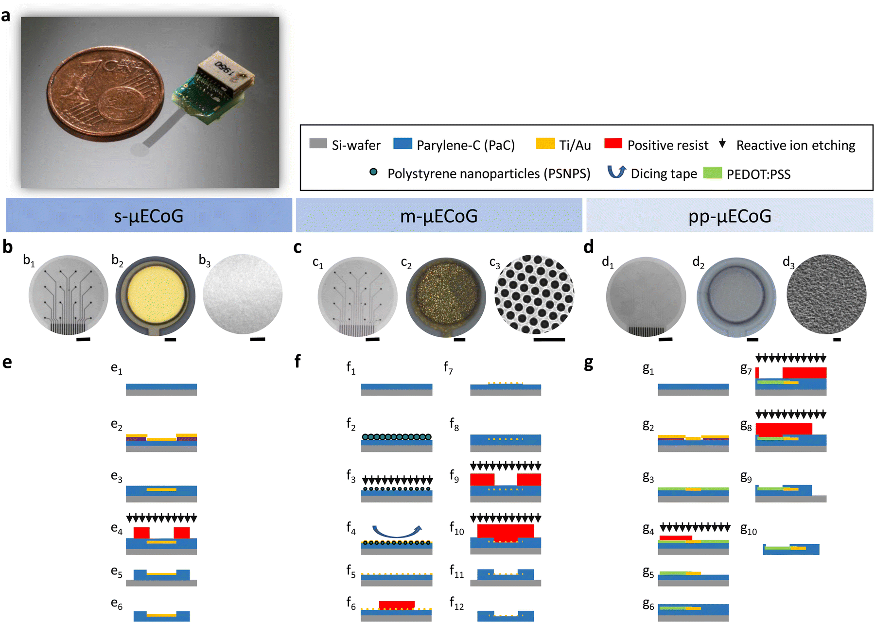 | ||
| Fig. 1 Design and fabrication of transparent flexible μECoGs. (a) Exemplary pp-μECoG with the corresponding packaging. All implants have a diameter of 2.6 mm and contain a matrix of 16 microelectrodes with a diameter of 50 μm and a pitch of 550 μm ((b1), (c1) and (d1); scale bar = 500 μm). Light microscopy and scanning electron microscopy (SEM) images of s-, m-, and pp-μECoG electrodes are shown in (b2), (c2) and (d2) (scale bar = 10 μm) and (b3),(c3) and (d3), (scale bar = 1 μm), respectively. The fabrication process flow for s-, m-, and pp-μECoGs is shown in (e), (f), and (g), respectively, starting with the deposition of a PaC layer via chemical vapour deposition (e1), (f1) and (g1). The fabrication of s-μECoGs was followed by the patterning of metal structures using a lift-off technique (e2) and the encapsulation by the deposition of a second PaC layer (e3). The shape of the implant, contact pads and electrode openings were exposed with reactive ion etching (RIE, (e4)), followed by the stripping of the photoresist etch mask (e5), and releasing of the implant from the host silicon wafer (e6). The fabrication of m-μECoGs included PSNPs that were deposited on a PaC-coated substrate. PSNPs were deposited using a funnel-assisted self-assembly process (f2). The PSNPs were then reduced in size with RIE (f3), evaporated with Ti/Au (f4), and stripped with dicing tape (f4) and (f5). The mesh structures were then patterned using a positive photoresist as an etch mask and removing the excess metal via wet chemical etching (f7). Then, a second PaC layer was deposited (f8), followed by two RIE steps, one for the passivation openings (f9), and one for the shape outline (f10), followed by photoresist removal (f11) and implant release (f12). In the case of pp-μECoGs, a first Ti/Au layer was structured with contact pads and feedlines via lift-off (g2). PEDOT:PSS was then spin-coated (g3) and a positive resist was used as an etch mask to expose parts of the feedlines and electrode sites, which were then patterned with RIE (g4) and photoresist removal (g5). After depositing a second PaC layer (g6), two RIE steps were performed to pattern the passivation (g7) and the shape of the implant (g8), remove the etch mask (g9), and release the implant (g10). | ||
As an example of a non-transparent implant, we fabricated s-μECoGs with electrical interconnects (feedlines) and electrodes made of solid metal layers consisting of Ti/Au (20/100 nm) using standard surface micromachining6,8 (Fig. 1e). To achieve transparent devices, we followed two materials strategies. The first strategy consisted of creating metallic nano-mesh (also named nanohole array) structures based on Au by combining standard photolithography with colloidal lithography. Here, we used polystyrene nanoparticles (PSNPs) as nano-templates to form the mAu that resulted in circular honeycomb-like metal structures (Fig. 1c3). The fabrication was adapted from previous work to match the fabrication process flow of flexible substrates.6,25
First, we deposited a monolayer of PSNPs on PaC-coated substrates using a funnel-assisted self-assembly process that traps the PSNPs at the water–air interface (Fig. S1a and b, ESI†). After reducing the size of the PSNPs with RIE, we coated them with Ti/Au and used dicing tape to lift the PSNPs (Fig. S1c, ESI†). We then removed the excess metal layers of the structure via wet chemical etching. To avoid the physical removal of the mesh electrodes, we implemented two RIE steps: the first one to allow the removal of PaC at the contact pad and electrode sites and the second one to outline the shape of the implant (Fig. 1f).
The advantage of this fabrication approach is that it avoids the use of toxic solvents, such as chloroform, to remove the PSNPs as proposed in other works.19 This is a significant advantage because such solvents can cause the swelling of PaC and other polymers.34,35 Therefore, our fabrication process avoids harmful reactions on the materials being used, making it suitable for the implementation on other soft polymeric materials beyond PaC, such as PDMS. Moreover, this process allows the fabrication of mAu feedlines and electrodes with different mesh-hole sizes. As an example, we obtained an average mesh-hole size of 275 ± 7.5 nm and 416 ± 31.5 nm with a lattice constant (original size of PSNPs) of 390 nm and 617 nm upon 4.5 min and 7 min of dry etching during size reduction, respectively (Fig. 1c and Fig. S1d, ESI†).
The second strategy comprised the combination of metal feedlines with bare PEDOT:PSS-based feedlines and electrodes, resulting in neural implants with strongly improved transparency (Fig. 1a and d). The fabrication was based on process flows proposed in the literature,22,27 in which PEDOT:PSS structures are patterned with dry etching techniques, such as RIE. To avoid etching PEDOT:PSS from the electrode sites, we implemented two RIE steps as performed for the m-μECoGs (Fig. 1g). After processing, PEDOT:PSS layers embedded in PaC (feedlines and edges of electrodes) and exposed PEDOT:PSS electrodes exhibited a thickness of 78 ± 7 nm and 39 – 52 nm, respectively (Fig. S2, ESI†). All fabrication processes can be transferred to other designs and applications.
3.2. Electrical and electrochemical performance of μECoGs
Considering that one of our aims is to couple electrically with nervous tissue and capture extracellular activity in the range of μV–mV, the electrical and electrochemical properties of the conductive materials used as feedlines and electrodes are of vital importance to ensure proper recording quality. In particular, we require highly conductive feedlines with a low lead resistance, below the impedance of our sensing electrodes, thereby reducing parasitic capacitances that result in crosstalk across channels.36 To this end, we validated the electrical properties of the proposed materials for our conductive feedlines, as well as the electrochemical performance of the materials proposed as recording electrodes.To validate the electrical properties of our conductive materials, we first simulated the influence of the mesh-hole size on the resistance of mAu feedlines using two different lattice constants when compared to sAu. As exhibited in Fig. 2a, the resistance of the feedline increases exponentially with the mesh-hole size. The bigger the mesh-hole, the more resistive the feedline. If the mesh size reaches the lattice constant (mesh-hole size = 100%), then the mesh is not conductive anymore, and the resistance tends to infinity. Moreover, considering that the exposed electrodes hold also the mesh structure and that the impedance of recording electrodes has an inversely proportional relationship with the geometric surface area (GSA) of the electrode, we simulated the GSA for sAu and for mAu with different mesh-hole radius ratios. The latter is defined as the ratio of mesh-hole radii over the lattice constant. Fig. 2b shows that there is indeed a geometrical window in which mAu electrodes, despite containing fewer metallic mass, have a GSA that is 1.13- to 1.32-fold higher than sAu electrodes, corresponding to mesh-hole radii of 17.8% and 33.7% with 617 nm and 390 nm lattices, respectively.
 | ||
| Fig. 2 Electrical and electrochemical performance of μECoGs. (a) Simulation of feedline resistance versus mesh-hole size for different mesh Au (mAu) structures in relationship to solid Au (sAu). The simulated feedlines comprise a length of 200 μm, a width of 3 μm, and a thickness of 100 nm for different mesh-hole sizes, which is a percentage over the lattice constants (d) of the mesh (original PSNP size). (b) Geometric surface area (GSA) versus mesh-hole radius ratio relationship for a 50 μm diameter recording electrode from sAu and mAu. (c) Conductivity of sAu, mAu, and PEDOT:PSS (PP) films on PaC-coated substrates (N = 6 for each electrode type). Impedance magnitude (d) and phase (e) of electrochemical impedance spectra for each implant type (Ns-μECoG = 31; Ns-μECoG-PP = 37; Nm-μECoG = 47; Nm-μECoG-PP = 58; Npp-μECoG = 99). m-μECoGs containing mAu electrodes with a lattice constant of 617 nm were selected for further use. To enhance the electrochemical properties, s-μECoG-PP and m-μECoG-PP contain an additional electro-polymerised PEDOT:PSS coating. Grey-shaded areas in (d) and (e) correspond to the frequency band (1 Hz–300 Hz) of interest for the recording of LFPs. | ||
While Au is known to be an excellent conductor, PEDOT:PSS is known to have a conductivity lower than metals but higher than many semiconductors and among the highest for polymers and quasi-metals. For example, the PEDOT:PSS solution used in this work exhibits a conductivity of 406 ± 53.5 S cm−1 (Fig. 2c), which is in range when compared to other works37,38 but still three orders of magnitude lower than solid Au (∼100000–338000 S cm−1, Fig. 2c). To increase the conductivity, PEDOT:PSS mixtures, such as the one used in this work, contain conductivity enhancing agents (e.g., ethylene glycol), as well as surfactants to facilitate film processing during spin-coating (e.g., dodecyl benzene sulfonic acid (DBSA)), and cross-linker agents (e.g., 3-glycidoxypropyltrimethoxysilane (GOPS)) to increase stability when immersed in electrolyte solutions.39 Nonetheless, when implementing long feedlines (e.g., long cables) made out only of PEDOT:PSS, we have to consider that the lead resistance falls on the order of 10.26 kΩ mm−1 (Table S1, ESI†). In practice, this means that for a 10.5 mm long cable, the lead resistance is 107.76 kΩ, which surpasses by 7-fold the theoretical impedance value at 1 kHz expected for a PEDOT:PSS electrode (∼15 kΩ) with a diameter of 50 μm and a thickness of 80 nm (Table S1, ESI†). Therefore, to further exploit other physical properties of this conductive polymer, the strategy of combining sAu feedlines with PEDOT:PSS electrodes appears currently unavoidable.
Considering that the quality of neuronal recordings with microelectrode arrays depends mainly on the impedance of the electrodes, we chose microelectrodes with a small diameter of 50 μm as a trade-off between low impedance versus spatial resolution. While bigger electrodes will present lower impedances, and therefore lower thermal noise, the spatial specificity during recordings will be reduced due to the electrical activity of distant cells that can still be picked up due to the size of the electrodes.40 Upon electrochemical characterization (Fig. 2d), all electrodes showed an impedance below 1 MΩ at 1 kHz, suitable for recording action potentials. Furthermore, the m-μECoGs exhibited an impedance even below s-μECoGs. This can be explained by the chosen mesh-hole radius of 197.5 nm for a lattice constant of 617 nm which falls in the geometrical window exposed before (∼32% mesh-hole radius ratio) that results in a bigger GSA than a sAu electrode of the same size. Additionally, it is also possible that mesh imperfections induce increases in the GSA, for example, in cases where the connection between two holes is broken (Fig. S1e, ESI†).
Given that the application of the tested implants is to capture epidural neural activity from the cortex, the signals of interest are low-frequency LPFs signals in a frequency band between 1 Hz and 300 Hz40 (grey band in Fig. 2d and e). In this range, both, s-μECoGs and m-μECoGs exhibit a high impedance on the order of hundreds of MΩ at 1 Hz. We, therefore, deposited an electrode coating based on electropolymerised PEDOT: PSS at the surface of sAu and mAu electrodes, reducing their impedance to ∼3 MΩ at 1 Hz, representing a 155- and 62-fold reduction for s-μECoGs and m-μECoGs, respectively.
In contrast, PEDOT:PSS (PP)-based electrodes presented an impedance of 28.8 ± 9 MΩ at 1 Hz and 147 ± 55 kΩ at 1 kHz, showing a resistive behaviour (phase close to zero, Fig. 2e) at high frequencies and a capacitive behaviour (phase closer to −90°, Fig. 2e) at lower frequencies, typical for PP-electrodes.41,42 However, although the impedances are in range for recording either action potentials or LFPs,43,44 the impedance is 9.5-fold higher than the calculated theoretical impedance when assuming the extended Stern model of a capacitor (see Materials and methods). This discrepancy could be either due to the lead resistance introduced by PEDOT:PSS feedlines or thickness variations upon fabrication.
Given that our pp-μECoG design has feedlines with a maximum length of 2431 μm, a width of 10 μm, and a thickness of 80 nm at the sensing area, the lead resistance of such feedlines can lead to impedance increases of up to 67 kΩ (Fig. S3, ESI†). Moreover, while we manufactured the PEDOT:PSS layers to be ∼80 nm (thickness of PEDOT:PSS layers fully encapsulated with PaC), the layer was almost half the expected thickness at the electrode openings (Fig. S2, ESI†). Such differences in PEDOT:PSS layer thickness can be a consequence of over-etching or to the exposure to different solvents, such as acetone, and deionised water. Especially deionised water can lead to pronounced thickness reductions, with decreases down to 60% of the original thickness.39 Since thickness reduction is not only solvent-dependent but additive (e.g., GOPS) dependent,39 further characterisation is needed to improve the microfabrication process on PEDOT:PSS layers, as the thickness of PEDOT:PSS follows an inversely proportional relation with impedance.41 Such shortcomings could be overcome by using solvents that are also conductivity enhancing agents, such as dimethyl sulfoxide (DMSO) or by implementing other processing technologies, such as orthogonal processing.22
As shown in Table 1, both m-μECoG-PP and pp-μECoG devices exhibited ideal electrochemical properties for the proposed application. Furthermore, the m-μECoG-PP, showed a specific impedance (Zspec) below those reported by earlier work, both at 1 kHz and 1 Hz. The latter is highly influenced by the thickness of the PEDOT:PSS layer, which was approximately 560 nm as reported before.45
| Reference | Electrode material | Electrode area [103 μm2] | Z@1 Hz [MΩ] | Z spec@1 Hz [kΩ × cm2] | Z@1 kHz [kΩ] | Z spec@1 kHz [mΩ × cm2] |
|---|---|---|---|---|---|---|
| The magnitude of the impedance (Z) and the specific impedance (Zspec) at 1 Hz and 1 kHz is compared for different electrode materials and areas proposed in the literature. | ||||||
| m-μECoG | m-Au | 2.06 | 201.34 | 4.14 | 515 | 10.58 |
| m-μECoG-PP | m-Au/PP | 1.96 | 3.22 | 0.06 | 9 | 0.18 |
| pp-μECoG | PP | 1.96 | 28.82 | 0.57 | 147 | 2.88 |
| Electrode Grid46 | Pt plated NWs | 3.00 | 1.00 | 0.03 | 10 | 0.30 |
| Opto-E-Dura20 | Pt particles | 94.25 | 0.03 | 0.02 | 1 | 0.94 |
| PEDOT:PSS MEAs22 | PP | 7.85 | 0.30 | 0.02 | 8 | 0.63 |
| Bilayer-nanomesh19 | m-Au/PP | 5.03 | 3.00 | 0.15 | 12 | 0.61 |
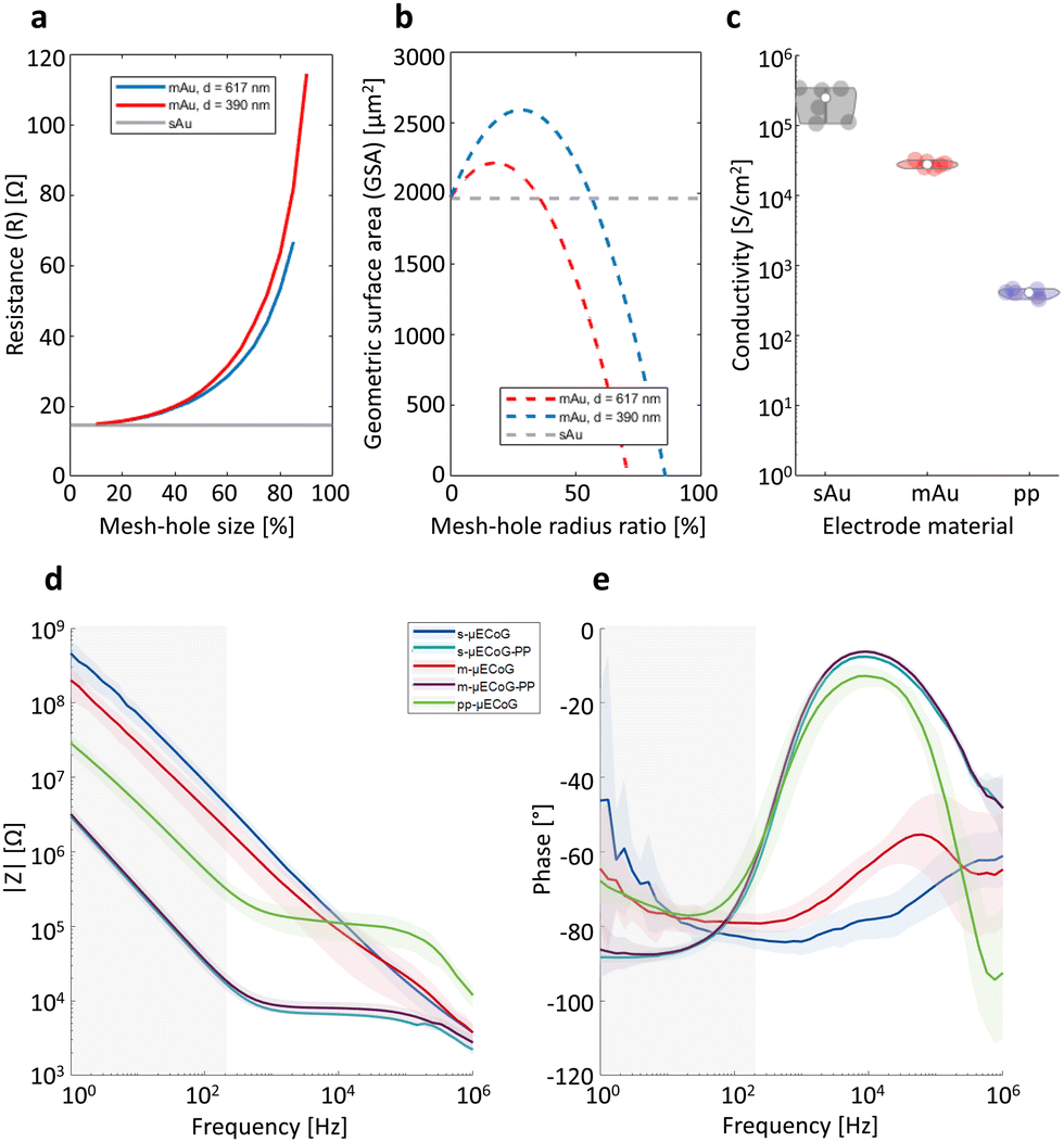
To optimally combine electro- and optophysiological measurements, other crucial features for multimodal neural implants are optical transparency and resistance against photo-induced artefacts. We, therefore, characterised the transparency of each μECoG type by measuring the light transmission of 10 μm thick-PaC, and 3 μm thick-PaC/sAu, PaC/mAu, and PaC/PP layers. The mean transmission at different light wavelengths (200–1000 nm) for three samples per material is shown in Fig. 3a. Note that all spectra of PaC-based layers exhibit interference fringes with varying amplitude and period, which results from infinite reflections occurring between the top and bottom surfaces of the thin film layer. Here, the thin film material is acting like an optical resonator given two parallel planes that are in a partially mirrored interface in an enclosed optical medium. These reflected waves interfere with each other and lead to the observed interferences in light transmission.47–50
 | ||
| Fig. 3 Optical performance of transparent and flexible μECoGs. (a) Optical transmission at different wavelengths for different electrode materials. Grey regions denote regions of interest for optical imaging and optogenetic stimulation were high transmittance is particularly desirable. (b) Left: Close-up images of fully assembled s-, m-, and pp-μECoG electrodes. Scale bar = 10 μm and 120 μm. Right: Widefield fluorescence (λ = 470 nm) and two-photon (λ = 920 nm) images from s-, m-, and pp-μECoG arrays, placed on an equifluorescent test slide. Images show electrodes either in focus (“Top focus”) or with the focus being 470 μm below the electrodes (“Bottom focus”), to assess shadows from electrodes and feedlines that could occlude functional imaging of the neural tissue below the array. Edges in the “Bottom focus” images are from markings on the test slide below the electrodes. (c) Quantification of the electrode shadows from s-, m-, and pp-μECoG arrays during widefield and two-photon imaging (N = 4 contacts per μECoG array type). | ||
As expected, the PaC/sAu had no detectable light transmittance across all wavelengths and PaC/PP showed consistently high transmittance. In comparison with the opaque metal, PaC alone exhibits strong absorption of UV light until 280 nm followed by a rapid increase reaching a mean of 80% transmittance at 352 nm. In contrast, the transmission spectrum of PaC/mAu had additional features, appearing as a dip at around 550 nm with a gradual increase of transmittance along longer wavelengths. This results in an average of 35.6 ± 0.3% and 61.8 ± 0.4% within the regions of interest for optophysiological applications (450–650 nm and 850–1000 nm, respectively). A weak peak at 450 nm is associated with the self-luminescence of Au while the transmittance peak at longer wavelengths originates from the excitation of surface plasmon polaritons. A hexagonal periodic two-dimensional pattern of holes contributes to the coupling of light to surface plasmons that exist in the metal and result in the increase of transparency.25 Moreover, the peak position can be tuned depending on the selected pitch and nano-mesh hole diameter (Fig. 3a). For mAu with a lattice constant of 390 nm, such a peak is encountered between 650–860 nm, while for a lattice constant of 617 nm, the peak is just starting to appear between 900–1000 nm. Given the higher transmittance exposed by mAu with a lattice of 617 nm, reaching a transmittance above 50% between 850–1000 nm, we chose this construct for further characterisation.
For functional imaging and optogenetic manipulation, the main region of interest is in the visible light between 450–650 nm11,12 (left grey region, Fig. 3a). Here, PaC/mAu-617 achieved a mean light transmittance of 35.6 ± 0.3% while PaC/PP was largely indistinguishable from PaC alone with a transmittance of 87.8 ± 0.3%. Both approaches therefore significantly improve the light transmittance of μECoG electrodes, making them promising candidates for combined electro- and optophysiological applications. The same is true for applications in the infrared range (850–1000 nm, right grey region, Fig. 3a), such as two-photon imaging, were light transmittance of PaC/mAu-617 was at 61.8 ± 0.4% while PaC/PP was at 89.1 ± 0.5%. The wavelength-dependence of light transmission with mAu structures depends on the exact parameters of the nano-mesh which can be optimized further by using different sizes (e.g., bigger nano-mesh holes or using a larger lattice constant) of PSNPs to achieve μECoG that are custom-tailored for specific imaging or optogenetic applications.
3.3. Optical transparency and signal attenuation during widefield and two-photon imaging
To evaluate the impact of different μECoG arrays on fluorescent imaging, we placed s-, m-, and pp-μECoG arrays on an equifluorescent microscope test slide and measured the intensity of emitted green fluorescence (between 500–550 nm) using blue excitation light at 470 nm (“Widefield”, Fig. 3b). Consistent with our transmission test, s-μECoGs blocked fluorescence light when in focus but some fluorescence signal could be recovered when moving the focal plane 470 μm below the electrodes. Similarly, fluorescence light attenuation from m-μECoGs and pp-μECoGs was reduced when imaging below the electrodes. To quantify the signal loss from electrode shadows, we computed the attenuation of fluorescence light as the difference between measured intensity directly under each electrode and its immediate surrounding (Fig. 3c and Fig. S4, ESI†). During widefield imaging, s-μECoGs still blocked a significant amount of light (attenuation = 54.7 ± 0.4%) whereas m-μECoGs and pp-μECoGs only weakly reduced fluorescence measurements (attenuation = 14.7 ± 1.7% and 2.5 ± 0.8%, respectively). Both approaches are therefore well suited to improve the quality of widefield imaging during combined electro- and optophysiological experiments.Signal attenuation was larger during two-photon imaging with excitation light at 920 nm: shadows from electrodes and feedlines were more clearly visible, even for the largely transparent pp-μECoG electrodes, and signal attenuation was generally increased (Fig. 3c, right). Fluorescence attenuation was highest under s-μECoGs electrodes (82.7 ± 0.5%) but also quite notable for m-μECoGs electrodes (63.2 ± 1.8%). As expected from our transmission test, fluorescence attenuation was lowest for pp-μECoGs electrodes (41.3 ± 1.8%).
3.4. Characterisation of photo-induced artefacts in saline solution
Shining light on electrodes creates a voltage or photocurrent that can strongly interfere with electrophysiological measurements.17 Aside from optical transparency, it is therefore crucial for neural implants to be largely resistant to this effect to allow simultaneous electrophysiological measurements during imaging or optogenetic stimulation. To test the robustness of s- and m-μECoG-PP and pp-μECoGs to photo-effects upon illumination, we exposed electrodes of each implant type to 10 ms long pulses of blue light (Fig. 4a) in saline solution. For each electrode type we observed a corresponding photo-induced artefact but with clear differences across materials: while s- and m-μECoG-PPs showed responses of similar magnitude to blue light pulses, pp-μECoG electrodes were largely unaffected. The magnitude of photo-induced artefacts was linearly related to the applied light power for all μECoG types (correlation coefficient rs-μECoGs = 0.96, rm-μECoGs = 0.97, rpp-μECoGs = 0.39) and largely similar for different wavelengths (Fig. 4b).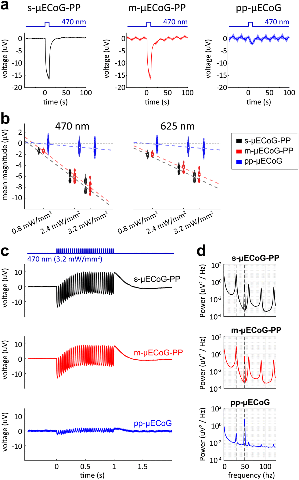 | ||
| Fig. 4 Characterization of light-induced artefacts in saline solution. Recording of light-induced artefacts from s-, m-, and pp-μECoG electrodes, in response to a 10-ms long light pulse (λ = 470 nm, irradiance = 3.2mW mm−2) in PBS. Average signals over 125 light pulses on 6 electrodes (N = 750 in total). (b) Mean magnitude of measured signals for s-, m-, and pp-μECoG electrodes in response to 10 ms long light pulse at different wavelengths (λ = 470 and λ = 625 nm) and different light power levels (N = 750 pulses per condition). Coloured dashed lines show linear regression line for each μECoG type. (c) Recording of light-induced artefacts from s-, m-, and pp-μECoG electrodes, in response to a 1 s long, 30 Hz stimulation sequence, as commonly used during functional imaging. Traces show average signals over 20 light sequences on 6 electrodes (N = 120 in total). (d) Power spectral density for each μECoG type during 30 Hz stimulation as shown in (c). Grey dashed lines indicate light-induced oscillations at 30 Hz and line noise at 50 Hz. | ||
Lastly, we tested if photo-induced artefacts are equally observed at higher stimulation frequencies. We, therefore, illuminated electrodes with 1 s long 30 Hz light sequences, as commonly used during functional imaging. As with single pulses, we found clear responses with comparable magnitude for s- and m-μECoG-PPs but only minor responses for pp-μECoGs (Fig. 4c). To quantify this effect, we computed the power spectral density for each μECoG type (Fig. 4d). Spectral power for s- and m-μECoG-PPs at 30 Hz was again largely comparable with 7.5 ± 1.3 μV2 Hz−1 and 6.8 ± 1.7 μV2 Hz−1, respectively. In contrast, 30 Hz spectral power for pp-μECoGs was barely measurable at 0.1 ± 0.1 μV2 Hz−1.
The generation of photo-induced artefacts in electro-physiological recordings has been attributed either to the Becquerel effect, the photoelectric effect, or to a combination of photoexcitation modes (e.g., photoelectrochemical, photo-conductive, photovoltaic, etc.), affecting mainly materials with no bandgap in its electronic structure, namely conductors such as Au. Given that the photon energy of the LED wavelengths (E470nm = 2.64 eV, E625nm = 1.98 eV) used in this work is below the work function of the metals in our implants (ΦTi = 4.33 eV, ΦTi = 5.1 eV),51 a pure photoelectric effect is discarded, unless multi-photon events occur. While the mechanisms behind such photo-effects are still poorly understood, from a materials perspective, a good strategy is to use transparent materials with a wide bandgap to hinder the absorption of photons at the wavelengths of interest, but conductive enough to allow electrical recordings, as stated before by Kozai and Vazquez.17
The electronic properties of semiconductors depend on the doping and mixture formulation of conducting polymers.17,52 Hence, PEDOT:PSS has been shown to possess a wide bandgap (Eg = 1.39–3.64 eV)53–56 and work function (ΦPP = 4.8–5.3 eV) that increases with film thickness and depends on the additives of the mixture52,57,58 but is below the photon energy of the wavelengths of interest. Such properties make PEDOT:PSS a good alternative to metal conductors, not only because of its transparent (Fig. 3a) but also because of its electronic characteristics. Our results are therefore in line with earlier work on the benefit of using PEDOT:PSS-based electrodes.22,59
Moreover PEDOT:PSS-based electrodes surpass the performance of other transparent materials, such as graphene, which has a work function in the range of PEDOT: PSS but no bandgap (Φgraphene = 4.6–5.16 eV).60,61 Lastly, although we have used PEDOT:PSS as an electrode coating for s- and m-μECoGs, the transparent layer allows light to hit the base metal electrodes, which are prone to photo-effects,17 thereby explaining the presence of photo-induced artefacts. Therefore, our results strongly suggest that pp-μECoGs are particularly well suited for combination with optophysiological methods due to their superior transparency and resistance against photo-induced artefacts.
3.5. Chronic implantation and in vivo validation
Our previous results suggest that pp-μECoGs are superior to m-μECoG-PPs for combined electro- and optophysiological experiments. However, the magnitude of photo-induced artefacts for m-μECoG-PPs was still fairly low at the tested light levels which are in a similar range as during widefield imaging.29 For optophysiological applications that require low light intensities m-μECoG-PPs might thus be a better choice due to their lower impedance and consequently improved signal-to-noise ratio compared to pp-μECoGs (Fig. 2d). Moreover, the in vivo lifetime of different μECoG electrode types, a major factor for their utility in chronic applications, is largely unknown.To directly test the functionality and long-term stability of pp-μECoGs and m-μECoG-PPs in vivo, we chronically implanted each μECoG type in transgenic mice. Mice expressed the calcium indicator GCaMP6s to subsequently perform electrophysiological recordings during functional widefield or two-photon imaging. Since both implant types are thin and flexible, we could easily place them on the dura over the visual and somatosensory cortex within a 3 mm wide craniotomy (Fig. 5a). The implants were then covered with a 0.1 mm thick cover glass, which was subsequently sealed and permanently fixed to the skull with dental cement. The PCB and Omnetics connector were also fixed to the skull using dental cement. As expected from the low weight and dimensions of the implant, implanted animals showed no visible impairments in behaviour or head and body posture after implantation.
 | ||
| Fig. 5 Surgery and physiological measures of pp-μEcoG and m-μEcoG-PP arrays. (a) Surgical procedure for chronic implantation of μECoG arrays. (a1) A 3 mm wide craniotomy was made over visual and somatosensory cortex of an adult mouse and the brain was covered with phosphate-buffered saline (PBS). The μECoG array was then placed to float on the PBS drop and positioned in the craniotomy centre. (a2) A 3 mm cover glass was placed on top of the implant and carefully pushed in the craniotomy. The cover glass was stabilized with a wooden holder. (a3) Tissue glue and dental cement was used to stabilize the cover glass and bind it to the skull. (a4) An exemplary pp-μECoG array after successful implantation. (a5) Schematic of the implanted mouse with a cranial window and neural implant on the left hemisphere and the corresponding Omnetics connector on the right. The small footprint of the device allows seamless applications in small animal models. (b) Physiological recording from a pp-μECoG electrode under isoflurane anaesthesia, 1 week after implantation. Clearly visible are changes in neural activity when anaesthesia was increased (‘Deep anaesthesia’) and subsequently reduced again (‘Anaesthesia’ and ‘Light anaesthesia’). (c) Same as in (b) but for an exemplary m-μECoG-PP electrode. (d) Same as in (b) but after 4 months of chronic implantation. (e) Same as in (c) but after 3 months of chronic implantation. | ||
After a one-week recovery period, we tested the functionality of the implants by anaesthetising the mice with 0.5–1% isoflurane in oxygen (Fig. 5b and c). In both μECoG types, we observed functional signals that were clearly modulated by the depth of isoflurane anaesthesia: during 1% isoflurane (‘anaesthesia’) signals showed strong oscillatory activity and large signal deflections that were strongly reduced when increasing the isoflurane concentration to 5% (‘deep anaesthesia’). Here, we observed increased low-frequency oscillations and strong attenuation of cortical signals, consistent with known effects of deep isoflurane anaesthesia.62,63 Cortical activity increased again when reducing the anaesthesia depth and showed increased high-frequency activity when further lowering the anaesthesia depth to 0.5% isoflurane (‘light anaesthesia’).
To assess the long-term stability of the μECoG arrays, we repeated our functional measurements after three and four months of chronic implantation, for pp-μECoGs and m-μECoG-PP, respectively. Although their overall noise floor was increased, we were still able to record clear changes in cortical signals due to changes in anaesthesia for most electrodes. This was also confirmed by additional impedance measurements, demonstrating that the impedance of most contacts was still in a usable range after several months of chronic implantation, exhibiting electrode functionality of up to 80% in one pp-μECoG and 50% in the m-μECoG (Fig. 5d, e and Fig. S5, ESI†).
Both μECoG types are therefore well-suited to chronically measure epidural cortical signals of mice, showing functionality until implant removal (up to 4.5 and 3.5 months for pp-μECoGs and m-μECoG-PP, respectively). Nonetheless, after one-month post-implantation, we observed that the PEDOT:PSS coating in six out of twelve visible electrode sites of the m-μECoGs-PP was not any more visible, most likely indicating degradation of the electrode coating (Fig. 6a). Moreover, the four electrodes that had a visible electrode coating were not further degraded after three months post-implantation, suggesting that the strongest electrode degradation occurred within the first month after implantation. In vivo observations were confirmed upon implant inspection after explantation (Fig. 6b). Here we encountered both degraded and intact electrode sites and confirmed the degradation of the electrodeposited PEDOT:PSS coating on mAu-based electrodes. In addition, SEM inspection revealed electrode coating degradation in a total of seven out of sixteen electrodes in the ex-planted m-μECoG-PP. Despite the coating degradation, the base mAu electrode stayed intact, making it still possible to carry out electrical measurements with the drawback that the quality of the recordings was strongly reduced, due to the high impedance that led to higher noise floor levels (Fig. S5, ESI†). In contrast, pp-μECoGs did not show signs of coating degradation (Fig. 6c and d), showing superior chronic stability. However, we observed some biological adsorption due chronic implantation (Fig. 6d2).
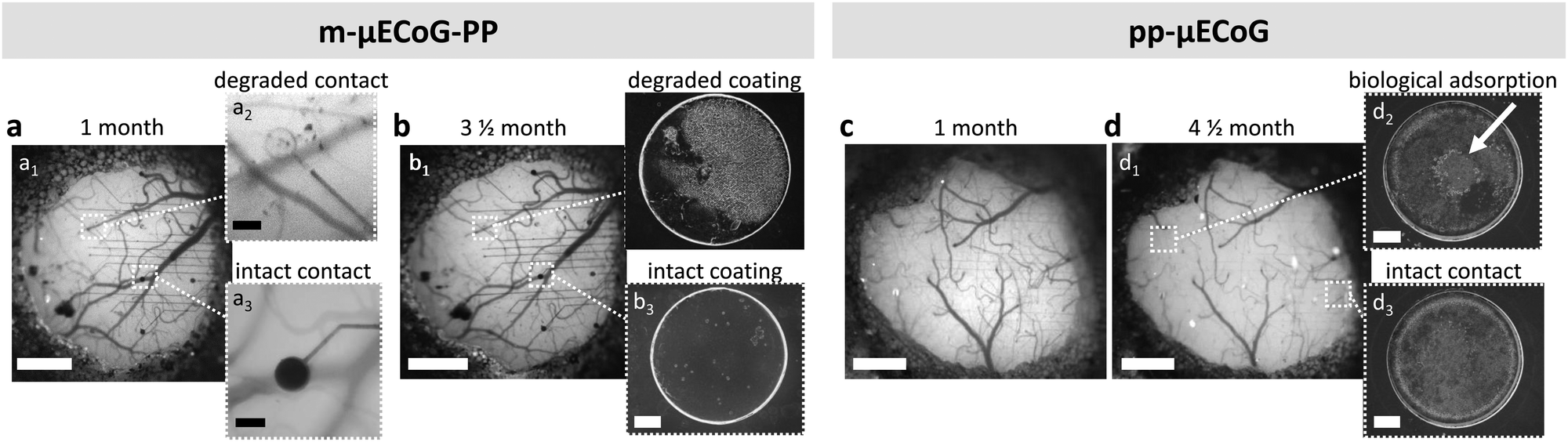 | ||
| Fig. 6 Chronic stability of μECoGs. (a) Widefield vessel image after one month (a1) and three-and-a-half-month post-implantation (b1). Red circles point out those electrical contacts that are degraded. Scale bar = 0.5 mm. Zoomed in degraded (a2) and intact contact (a3). Scale bar = 50 μm. The degradation signs exhibited by m-μECoG-PP are stagnating after one month-implantation. (b2) Scanning electron microscopy (SEM) images exposing exemplary electrical contacts of a m-μECoG-PP with a degraded (b2) and intact (b1) PEDOT:PSS coating after three-and-a-half month post-implantation. Widefield vessel image of pp-μECoG one month (c) and four-and-a-half-month (d1) post-implantation. (d2) and (d3) SEM images of an biological adsorption on an intact electrode contact and an intact contact without residues of a pp-μECoG four and a half months post-implantation. Scale bar of SEM pictures = 10 μm. | ||
3.6. Electrophysiological measurements of multi-area cortical activity with simultaneous functional widefield and two-photon imaging
A major advantage of using μECoG arrays in small animal models is their ability to resolve fine spatial differences in cortical activity to obtain spatial maps of cortical response patterns, e.g., neural responses to sensory stimulation. We, therefore, performed combined electrophysiology and functional widefield measurements in response to either visual or tactile stimulation in awake mice. Since the cranial window provided access to up to seven separate cortical regions (see Allen mouse atlas64 with window location in Fig. 7a), this allowed us to simultaneously measure sensory responses across these cortical regions with both electrophysiology and functional imaging.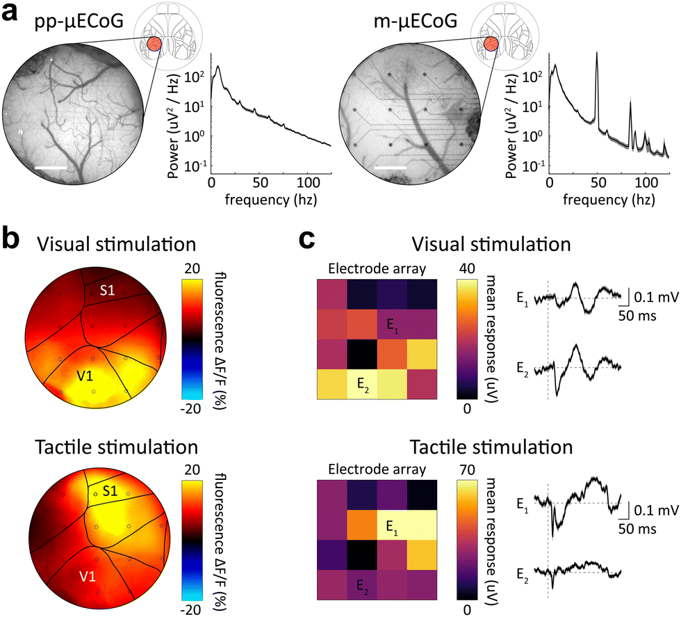 | ||
| Fig. 7 Simultaneous μECoG and widefield recordings in awake mice. (a) Example vessel images of pp-μECoG (left) and m-μECoG (right) array that was chronically implanted over V1 and S1 cortex of a GCaMP6s-expressing mouse and correlated power spectra. Scale bar = 0.5 mm. (b) Changes in fluorescence signals during widefield imaging in response to either visual or tactile stimulation. Images show average responses over 75 stimulus presentations. Dots indicate the location of the recording electrodes matching the maps in c. (c) Average event-related potentials as measured with the pp-μECoG array. Matrices on the left show the mean response magnitude within 100 ms after stimulus presentation. Traces on the right show example recordings from electrodes that preferentially respond to tactile (E1) or visual stimulation (E2). | ||
Consistent with our earlier characterization of photo-induced artifacts (Fig. 4), pp-μECoG electrodes showed only minor responses to excitation light pulses during imaging (Fig. 7a). The same was true for m-μECoG-PPs, confirming that this electrode type can also be used with widefield imaging at low light powers (Fig. S6, ESI†). In agreement with the anatomical location of cortical areas,64 widefield imaging showed clear responses to visual stimulation in the posterior primary visual cortex (V1) while tactile stimulation evoked stronger responses in the more anterior somatosensory cortex (S1, Fig. 7b). The same spatial pattern was revealed when computing event-related potentials (ERPs) over all pp-μECoG contacts (Fig. 7c) in the simultaneously acquired electrophysiological recordings, demonstrating that pp-μECoG are a valuable tool for mapping neural responses across cortical areas.
Tactile ERPs were also faster and more temporally precise (peak response = 11.4 ms, full-width half-maximum = 7.4 ms) as visual ERPs (peak response = 40.1 ms, full-width half-maximum = 25.6 ms), which is in good agreement with known response latencies of sensory responses in somatosensory65 and visual cortex,66 respectively. Similar results were observed with m-μECoG-PP electrodes, although the spatial map of cortical responses was not as well separated. This was likely due to degradation of several electrical contacts, which exhibited unstable PEDOT:PSS coating on the mAu electrodes and poor recording quality after one month implantation (Fig. 6a and b). Nonetheless, these results demonstrate that both pp- and m-μECoG-PPs can be utilized to chronically perform simultaneous electro- and opto-physiological measurements of sensory-evoked cortical activity patterns in awake mice with minimal photo-induced artefacts or optical interference.
Moving beyond population signals with widefield imaging, we sought to directly relate our electrophysiological measures to the activity of individual cortical neurons. We therefore tested the in vivo utility of pp- and m-μECoG-PP arrays in combination with two-photon imaging which can measure the activity of large neural networks with single cell resolution. Both μECoG types showed mild auto-fluorescence and were visible in the green emission channel (λ = 500–550 nm) of the microscope (Fig. 8a and Fig. S7a, ESI†). Directly scanning over an example electrode caused a notable photo-induced artefact at the imaging rate (30 Hz) and corresponding resonant frequencies, which was most pronounced at the surface of the imaged electrode, especially in m-μECoG-PP (Fig. 8b and Fig. S7b, ESI†). Imaging 200 μm below the brain surface reduced the artefact magnitude but it remained notable in both electrode types. No photo-induced artefacts were observed in adjacent electrodes, demonstrating that this effect only occurred when the imaging laser was directly scanning over a given electrode.
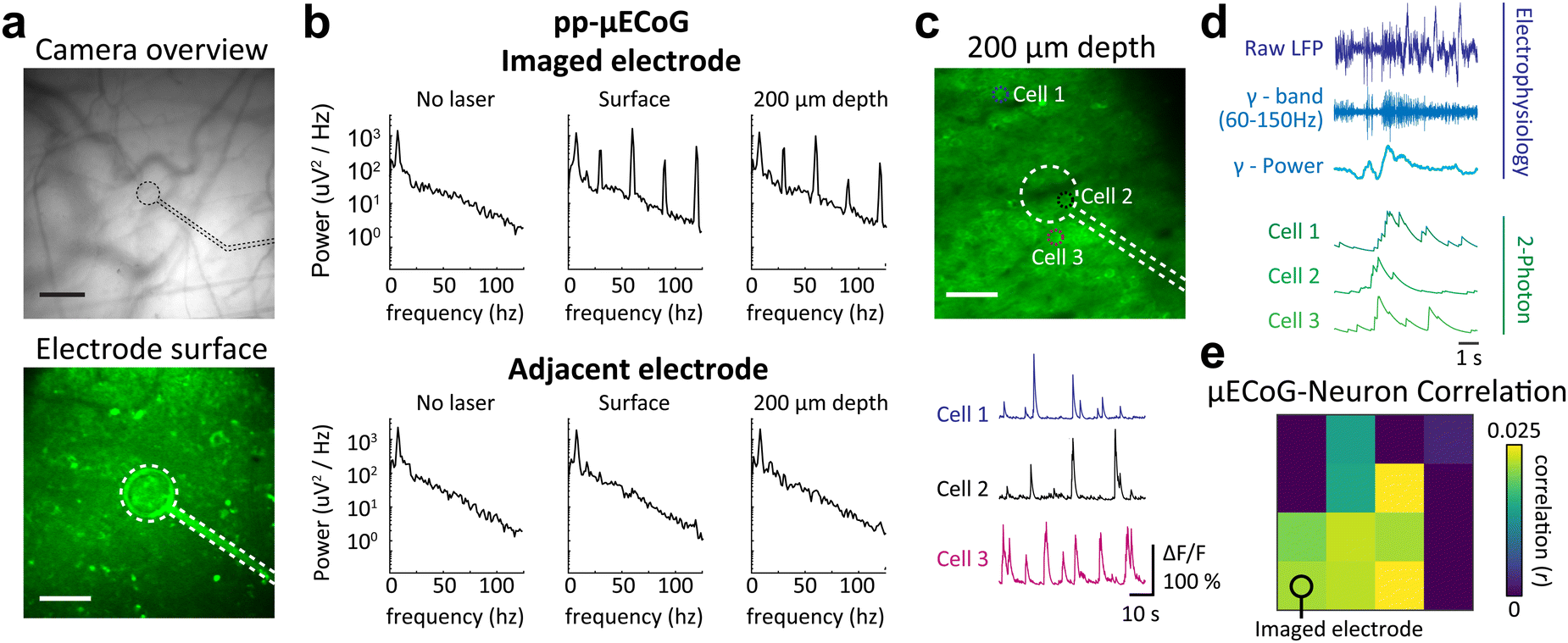 | ||
| Fig. 8 Simultaneous μECoG and two-photon recordings in awake mice. (a) Top: Fluorescent vessel image of a chronically implanted pp-μECoG electrode over somatosensory cortex. Black dashed lines indicate location of the transparent electrode. Scale bar = 100 μm. Bottom: Two-photon image of the same electrode as in the top image. Scale bar = 50 μm. (b) Power spectral density of the electrode shown in (a) and an adjacent electrode during different stages of imaging. Spectra on the left were taken before imaging was started, spectra in the middle while focusing the laser directly on the electrode, and spectra on the right while imaging 200 μm below the electrode. (c) Same imaging location as the bottom image in (a) but focused 200 μm below the electrode. Dashed circles indicate the location of 3 example cells for which functional signals are shown below. Cell 2 was imaged directly below the electrode. (d) Example traces from raw μECoG recording (violet, top) with the gamma-band filtered signal and gamma power envelop (dark and light blue traces, respectively). The bottom traces in green show calcium-related fluorescence changes of three example cells that were simultaneously recorded with two-photon imaging. (e) Average correlation of gamma power in each μECoG electrodes and all neurons measured with two-photon imaging. The imaged electrode marks the location in visual cortex V1, where two-photon imaging was performed. The μECoG electrode location in other cortical areas are also shown as circles in Fig. 7b. | ||
Importantly, the pp-μECoG arrays caused no visible perturbation of the imaging signal at 200 μm imaging depth and no shadows were visible underneath the electrode or feedlines. Correspondingly, we were able to extract clear calcium dynamics from individual neurons throughout the field of view and could even identify neural activity from directly underneath the imaged electrode (‘Cell 2’, Fig. 8c). The neural dynamics from underneath the electrode exhibited similar changes in fluorescence as observed in other neurons that were either close or further away from the electrode (‘Cell 3’ and ‘Cell 1’, respectively). The signal quality of the two-photon imaging even exceeded promising results from earlier work41 and demonstrates that pp-μECoG arrays are particularly well-suited for combined applications with functional imaging.
In contrast, the m-μECoG-PP electrode and feedlines created a visible shadow in the field of view and no neurons could be identified in the affected areas. However, signals from neurons in the immediate proximity of the electrode were not affected and showed clear fluorescence signals (Fig. S7, ESI†). Together, these results show that m-μECoG-PP electrodes are also usable during two-photon imaging but were inferior to pp-μECoG electrodes which caused no notable impairment in imaging quality.
Lastly, we further analysed our simultaneously acquired electrophysiology and two-photon data to assess if the activity of individual neurons is indeed related to surface ECoG signals. We therefore band-pass filtered the raw signal from all μECoG electrodes in the high-frequency gamma range (60–150 Hz), which has been shown to be correlated to the activity of individual cortical neurons.67,68 Indeed, we found that several individual neurons were correlated to gamma power of the nearest μECoG electrode (Fig. 8d). The close link between both measures demonstrates that combined electro- and optophysiological recordings can be used to relate activity of individual neurons to population signals across cortical regions. Plotting the average correlation of all imaged neurons to the gamma power in all μECoG electrodes also revealed an intricate spatial structure, with neurons being mostly correlated to μECoG electrodes that were close to the imaging site (Fig. 8e, bottom left). Interestingly, the spatial pattern of correlations between μECoG signals and individual neurons matched the shape of the primary visual cortex where the two-photon imaging was done (see also location of V1 in Fig. 7b), suggesting that neural activity was most correlated to μECoG signals from the same cortical area. These results therefore demonstrate that combined recordings are a powerful tool to relate individual neurons to macroscopic μECoG signals and can reveal intricate details of cortical activity patterns within and across different cortical areas.
4. Conclusions
Towards the goal of determining the most suitable materials for combined neurophysiology and neuroimaging for acute and chronic in vivo neural applications, flexible and transparent neural implants are desired to overcome the optical and spatio-temporal limitations of individual modalities. If achieved, synchronised electrical and calcium activity could provide simultaneous insights into single-neuron and neuronal network dynamics in different brain regions only limited by the design and placement of the μECoG.Keeping in mind a functional validation, simultaneous access to different brain regions during electrophysiology was desired. Therefore, we chose the development of surface cortical electrode arrays such as μECoGs, selecting an electrode distribution that covered multiple cortical regions: somatosensory and visual cortex. Likewise, aiming for both acute and chronic applications, we chose PaC as substrate and encapsulation of the implants due to its known biocompatibility and conformability with neural tissue.69 Moreover, we chose Au and PEDOT:PSS as conductive layers due to their electrical and optical properties. Hence, we followed two different material-based strategies for the fabrication and in vitro and in vivo validation of flexible and transparent neural implants: (i) the implementation of metallic mesh structures as feedlines and electrodes made out of mAu (m-μECoG) and ii) the implementation of sAu feedlines with plain PEDOT:PSS electrodes (pp-μECoG). As a reference of a non-transparent implant, μECoGs with sAu (s-μECoG) were also investigated.
Fabrication-wise, we provide a novel and simplified process flow for both m-μECoGs and pp-μECoGs to avoid toxic chemicals and to allow the use of standard photoresists, respectively. Our proposed process flow for m-μECoGs allows to use the same material as substrate and encapsulation, non-toxic solvents, and standard photoresists. Furthermore, the use of PSNPs offers the possibility of tuning the mesh-hole size by the selection of a suitable mesh lattice constant and adjusting dry etching times. The proper selection of the mesh-hole size can lead to optimized optical, electrical, and electrochemical properties. For example, bigger holes lead to enhanced transparency but increase resistance, and given the selected thickness, a geometrical window allows increasing the GSA of a mAu-based electrode which can lead to reduced impedance.
Moreover, the process flow of pp-μECoGs is implemented with broadly available standard photoresists. Hence, both fabrication processes have the potential to be transferred to other implant materials, designs, and applications. This is an important future direction our research group is already working on.6,8 The goal is to cover the three-dimensional space of the brain with μECoGs and intracortical implants while enabling a combined application of simultaneous distinct electrophysiology, functional imaging, and optogenetics.
During the production of fully transparent implants, we faced electrical limitations due to the low conductivity of PEDOT:PSS. Given that cables with a length between 7.5–10 mm are needed to connect the implant to an external electrical system while allowing enough room for imaging, plain PEDOT:PSS was not an option for long feedlines as a high lead resistance could lead to crosstalk. We, therefore, implemented pp-μECoGs that exploit the excellent conductivity of sAu for long feedlines, as well as the high transparency of plain PEDOT:PSS for short feedlines and electrodes at the sensing area. Notably, the use of dry etching and different solvents during fabrication might have affected the end thickness of the PEDOT:PSS layer, therefore directly impacting the impedance with a larger spread and higher than those reported in the literature. Nonetheless, PEDOT:PSS electrodes exhibited electrochemical properties in a suitable range for electrical recording of neural activity. Furthermore, the impedances of sAu and mAu electrodes were initially higher than PEDOT:PSS electrodes, and an electrode coating was added by the electropolymerization of PEDOT:PSS on sAu and mAu, achieving impedances below plain PEDOT:PSS electrodes without affecting the transparency of the electrodes.
Furthermore, optical characterisations in vitro revealed minimal (below 20%) fluorescence attenuation of pp-μECoGs and m-μECoGs during widefield imaging but an increased attenuation for two-photon imaging, which was still below 50% for pp-μECoGs, but higher for m-μECoG-PPs. Conversely to sAu and mAu electrodes, negligible photo-induced artefacts were observed on PEDOT:PSS electrodes, which exhibit electronic properties that shields the photoexcitation of the material at the tested wavelengths of interest.
Going one step further, we validated the transparent μECoGs in vivo and performed functional tests to proof the functionality of the implants. Here, both, m-μECoG-PPs and pp-μECoGs allowed the spatiotemporal correlation of neural activity upon tactile and visual activity, allowing the creation of functional maps based on functional imaging and electrical readings assigned to different channels and therefore brain regions. However, m-μECoG-PPs started showing signs of degradation at the electrode sites after one-month post-implantation, hindering the creation of functional maps during longer implantation times. On the other hand, pp-μECoGs showed up to 80% electrode functionality even after four-months post-implantation. Moreover, during two-photon imaging, in vitro predictions were confirmed. While the signal attenuation generated by m-μECoG-PPs was still good enough to image neurons at the immediate vicinity of the electrode, it was only possible to image a neuron right below the electrode of interest with pp-μECoGs.
The implementation of transparent μECoGs, as well as their in vitro and in vivo validation carried out in this work revealed that the development of flexible and transparent neural implants comprises the trade-off between electrical, electrochemical, and optical properties of both the implant and electrode materials, leading to the use of material combinations to exploit their different physical properties as required. Following such a strategy, our results show that pp-μECoGs have the best material properties trade-off for multimodal neurophysiological experiments in several important aspects. First, pp-μECoGs outperformed the functionality of s- and m-μECoG-PPs in saline solution by exhibiting a good range of impedance for electrical recordings and reduced fluorescence attenuation and photo-induced artefacts upon light exposure at different wavelengths. Second, pp-μECoGs showed a superior chronic in vivo stability than m-μECoGs-PP for up to four and half months. Moreover, pp-μECoGs revealed the advantages obtained when using combined electrophysiology with functional calcium imaging by allowing the creation of functional maps relating calcium signals, from both widefield and two-photon imaging, to electrical neural activity across multiple brain regions.
We performed a detailed functional mapping of sensory responses across multiple cortical regions and directly related the sensory responses from calcium transients with widefield imaging to electrophysiology. Such mapping demonstrates the feasibility of simultaneous multimodal recordings of functional cortical activity and allows the combination of high spatiotemporal resolution and cell-type specificity of calcium widefield imaging with the high temporal resolution of electrophysiological signals. Such combined recordings are highly valuable for studies of cortical signal processing and spatiotemporal spread of cortical activity. Moreover, our work also contributes to future multimodal studies on the generation of ECoG signals, e.g. due to contributions from different neural cell types in the cortex, which are of high translational value when using ECoG signals as a diagnostic tool in a clinical setting.
Moreover, we also directly related two-photon functional signals to electrophysiology by computing the correlation of individual neurons to the gamma-band power of individual μECoG channels. We found that this approach reveals a clear spatial relationship between individual cortical neurons and μECoGs electrodes, especially for electrodes over the same cortical area, and is therefore of high value for future studies that seek to understand the relation between single-cell and macroscopic population signals.
Finally, we showed that pp-μECoGs allowed the possibility of imaging neurons directly below the electrical contact of interest during two-photon imaging, unveiling important transparency features that are relevant when further increasing the electrode density of the implants, as these will be mostly covered by feedlines and electrodes sites.
Author contributions
L. K., S. M., and V. R. M. planned the study. B. L, D. M., A. O., and V. R. M. conceived the development of m-μECoGs. L. K., A. O., and V. R. M. conceived the development of pp-μECoGs. L. K. fabricated and characterised the neural probes with the support of M. J., S. M., and V. R. M. S. M. performed the animal experiments with the support of L. K., I. L., and V. R. M. Data processing and its corresponding analysis was performed by L. K., S. M., I. L., B. K., and V. R. M. L. K., S. M., and V. R. M wrote the initial draft of the manuscript. All authors reviewed and edited the manuscript. S. M. and V. R. M. co-supervised the study.Conflicts of interest
There are no conflicts to declare.Acknowledgements
We thank the Helmholtz Nano Facility (HNF) at Forschungszentrum Jülich for facilitating the microfabrication of neural probes. Special thanks to Dr. Vanessa Maybeck for infrastructural and scientific support; to Dongmei Mo and Zidu Li, former colleagues who worked in the development of the m-μECoGs; to Matthias Jenne former colleague who worked on the transmittance and light interference setups; to Bettina Breuer and Sandra Brill for invaluable support in organizing project procedures; to Elke Brauweiler-Reuters for performing FIB sectioning; to Dr. Jhih-Sian Tu for supporting the conductivity measurements; and Michael Prömpers, Regina Stockmann, and Marko Banzet for technical support at the HNF. This study was supported by the Deutsche Forschungsgemeinschaft (DFG, German Research Foundation; 368482240/GRK2416/424556709/GRK2610) and the Helmholtz association (VH-NG-1611).References
- M. Scanziani and M. Häusser, Electrophysiology in the age of light, Nature, 2009, 461(7266), 930 CrossRef CAS PubMed.
- G. Buzsáki, Large-scale recording of neuronal ensembles, Nat. Neurosci., 2004, 7(5), 446 CrossRef PubMed.
- H. Lüders, I. Awad, R. Burgess, E. Wyllie and P. Van Ness, Subdural electrodes in the presurgical evaluation for surgery of epilepsy, Epilepsy Res., Suppl., 1992, 5, 147 Search PubMed.
- D. R. Nair, R. Burgess, C. C. McIntyre and H. Lüders, Chronic subdural electrodes in the management of epilepsy, Clin. Neurophysiol., 2008, 119(1), 11–28 CrossRef PubMed.
- S. J. Groiss, L. Wojtecki, M. Südmeyer and A. Schnitzler, Deep Brain Stimulation in Parkinson's Disease, Ther. Adv. Neurol. Disord., 2009, 2(6), 20 CAS.
- V. Rincón Montes, J. Gehlen, S. Ingebrandt, W. Mokwa, P. Walter and F. Müller, Development and in vitro validation of flexible intraretinal probes, Sci. Rep., 2020, 10(1), 19836 CrossRef PubMed.
- D. Kuzum, H. Takano, E. Shim, J. C. Reed, H. Juul and A. G. Richardson, Transparent and flexible low noise graphene electrodes for simultaneous electrophysiology and neuroimaging, Nat. Commun., 2014, 5(1), 5259 CrossRef CAS PubMed.
- K. Srikantharajah, R. Medinaceli Quintela, K. Doerenkamp, B. M. Kampa, S. Musall and M. Rothermel, Minimally-invasive insertion strategy and in vivo evaluation of multi-shank flexible intracortical probes, Sci. Rep., 2021, 11(1), 18920 CrossRef CAS PubMed.
- M. Vomero, M. F. Porto Cruz, E. Zucchini, F. Ciarpella, E. Delfino and S. Carli, Conformable polyimide-based μECoGs: Bringing the electrodes closer to the signal source, Biomaterials, 2020, 255, 120178 CrossRef CAS PubMed.
- M. Vomero, F. Ciarpella, E. Zucchini, M. Kirsch, L. Fadiga and T. Stieglitz, On the longevity of flexible neural interfaces: Establishing biostability of polyimide-based intracortical implants, Biomaterials, 2022, 281, 121372 CrossRef CAS PubMed.
- O. Yizhar, L. E. Fenno, T. J. Davidson, M. Mogri and K. Deisseroth, Optogenetics in neural systems, Neuron, 2011, 71(1), 9–34 CrossRef CAS PubMed.
- T. W. Chen, T. J. Wardill, Y. Sun, S. R. Pulver, S. L. Renninger and A. Baohan, Ultrasensitive fluorescent proteins for imaging neuronal activity, Nature, 2013, 499(7458), 295–300 CrossRef CAS PubMed.
- J. B. Wekselblatt, E. D. Flister, D. M. Piscopo and C. M. Niell, Large-scale imaging of cortical dynamics during sensory perception and behavior, J. Neurophysiol., 2016, 115(6), 2852 CrossRef CAS PubMed.
- S. Musall, X. R. Sun, H. Mohan, X. An, S. Gluf and S. J. Li, Pyramidal cell types drive functionally distinct cortical activity patterns during decision-making, Nat. Neurosci., 2023, 1–11 Search PubMed.
- F. Helmchen and W. Denk, Deep tissue two-photon microscopy, Nat Meth., 2005, 2(12), 932 CAS.
- C. Grienberger, A. Giovannucci, W. Zeiger and C. Portera-Cailliau, Two-photon calcium imaging of neuronal activity, Nat. Rev. Methods Primers, 2022, 2(1), 1–23 CrossRef.
- T. D. Y. Kozai and A. L. Vazquez, Photoelectric artefact from optogenetics and imaging on microelectrodes and bioelectronics: new challenges and opportunities, J. Mater. Chem. B, 2015, 3(25), 4965 RSC.
- M. J. Donahue, A. Kaszas, G. F. Turi, B. Rózsa, A. Slézia and I. Vanzetta, Multimodal Characterization of Neural Networks Using Highly Transparent Electrode Arrays, Eneuro, 2018, 5(6), 0187-18.2018, DOI:10.1523/ENEURO.0187-18.2018.
- Y. Qiang, P. Artoni, K. J. Seo, S. Culaclii, V. Hogan and X. Zhao, Transparent arrays of bilayer-nanomesh microelectrodes for simultaneous electrophysiology and two-photon imaging in the brain, Sci. Adv., 2018, 4(9), eaat0626 CrossRef CAS PubMed.
- A. F. Renz, J. Lee, K. Tybrandt, M. Brzezinski, D. A. Lorenzo, M. Cerra Cheraka, J. Lee, F. Helmchen, J. Vörös and C. M. Lewis, Opto-E-Dura: A Soft, Stretchable ECoG Array for Multimodal, Multiscale Neuroscience, Adv. Healthcare Mater., 2020, 9(17), 2000814 CrossRef CAS PubMed.
- D. W. Park, A. A. Schendel, S. Mikael, S. K. Brodnick, T. J. Richner and J. P. Ness, Graphene-based carbon-layered electrode array technology for neural imaging and optogenetic applications, Nat. Commun., 2014, 5(1), 5258 CrossRef CAS PubMed.
- G. Dijk, A. Kaszas, J. Pas and R. P. O’Connor, Fabrication and in vivo 2-photon microscopy validation of transparent PEDOT:PSS microelectrode arrays, Microsyst. Nanoeng., 2022, 8(1), 90 CrossRef CAS PubMed.
- W. Albrecht, J. Moers and B. Hermanns, HNF - Helmholtz Nano Facility, J. Large-Scale Res. Facil., 2017, 3, A112 CrossRef.
- S. Middya, V. F. Curto, A. Fernández-Villegas, M. Robbins, J. Gurke and E. J. M. Moonen, Microelectrode Arrays for Simultaneous Electrophysiology and Advanced Optical Microscopy, Adv. Sci., 2021, 8(13), 2004434 CrossRef CAS PubMed.
- T. J. J. Hondrich, B. Lenyk, P. Shokoohimehr, D. Kireev, V. Maybeck and D. Mayer, MEA Recordings and Cell–Substrate Investigations with Plasmonic and Transparent, Tunable Holey Gold, ACS Appl. Mater. Interfaces, 2019, 11(50), 46451 CrossRef CAS PubMed.
- A. J. Bard and L. R. Faulkner, Electrochemical Methods: Fundamentals and Applications, John Wiley & Sons, Inc, 2nd edn, 2001 Search PubMed.
- P. Oldroyd, J. Gurke and G. G. Malliaras, Stability of Thin Film Neuromodulation Electrodes under Accelerated Aging Conditions, Adv. Funct. Mater., 2023, 33(1), 2208881 CrossRef CAS.
- S. Musall, M. T. Kaufman, A. L. Juavinett, S. Gluf and A. K. Churchland, Single-trial neural dynamics are dominated by richly varied movements, Nat. Neurosci., 2019, 22(10), 1677 CrossRef CAS PubMed.
- J. Couto, S. Musall, X. R. Sun, A. Khanal, S. Gluf and S. Saxena, Chronic, cortex-wide imaging of specific cell populations during behavior, Nat. Protoc., 2021, 1–25 Search PubMed.
- E. H. Ratzlaff and A. Grinvald, A tandem-lens epifluorescence macroscope: hundred-fold brightness advantage for wide-field imaging, J. Neurosci. Methods, 1991, 36(2–3), 127 CrossRef CAS PubMed.
- D. H. Brainard The Psychophysics Toolbox. Spat Vis. 1997;10(4):433.
- D. G. Pelli The VideoToolbox software for visual psychophysics: transforming numbers into movies. Spat Vis. 1997;10(4):437.
- M. Pachitariu, C. Stringer, S. Schröder, M. Dipoppa, L. F. Rossi and M. Carandini, u. a. Suite2p: beyond 10,000 neurons with standard two-photon microscopy, bioRxiv, 2016, 061507 Search PubMed.
- J. N. Lee, C. Park and G. M. Whitesides, Solvent Compatibility of Poly(dimethylsiloxane)-Based Microfluidic Devices, Anal. Chem., 2003, 75(23), 6544 CrossRef CAS PubMed.
- H. C. Koydemir, H. Kulah and C. Ozgen, Solvent Compatibility of Parylene C Film Layer, J. Microelectromech. Syst., 2014, 23(2), 298–307 CAS.
- M. E. J. Obien, K. Deligkaris, T. Bullmann, D. J. Bakkum and U. Frey, Revealing neuronal function through microelectrode array recordings, Front. Neurosci., 2015, 8 DOI:10.3389/fnins.2014.00423.
- Y. Xia and J. Ouyang, Significant Different Conductivities of the Two Grades of Poly(3,4-ethylenedioxythiophene):Poly(styrenesulfonate), Clevios P and Clevios PH1000, Arising from Different Molecular Weights, ACS Appl. Mater. Interfaces, 2012, 4(8), 4131 CrossRef CAS PubMed.
- H. Shi, C. Liu, Q. Jiang and J. Xu, Effective Approaches to Improve the Electrical Conductivity of PEDOT:PSS: A Review, Adv. Electron. Mater., 2015, 1(4), 1500017 CrossRef.
- S. Zhang, P. Kumar, A. S. Nouas, L. Fontaine, H. Tang and F. Cicoira, Solvent-induced changes in PEDOT:PSS films for organic electrochemical transistors, APL Mater., 2015, 3(1), 014911 CrossRef.
- V. Viswam, M. E. J. Obien, F. Franke, U. Frey and A. Hierlemann, Optimal Electrode Size for Multi-Scale Extracellular-Potential Recording From Neuronal Assemblies, Front. Neurosci., 2019, 13, 385 CrossRef PubMed.
- G. Dijk, H. J. Ruigrok and R. P. O’Connor, Influence of PEDOT:PSS Coating Thickness on the Performance of Stimulation Electrodes, Adv. Mater. Interfaces, 2020, 7(16), 2000675 CrossRef CAS.
- M. Ganji, A. T. Elthakeb, A. Tanaka, V. Gilja, E. Halgren and S. A. Dayeh, Scaling Effects on the Electrochemical Performance of poly(3,4-ethylenedioxythiophene (PEDOT), Au, and Pt for Electrocorticography Recording, Adv. Funct. Mater., 2017, 27(42), 1703018 CrossRef.
- J. A. Hosp, K. Molina-Luna, B. Hertler, C. O. Atiemo, A. Stett and A. R. Luft, Thin-film epidural microelectrode arrays for somatosensory and motor cortex mapping in rat, J. Neurosci. Methods, 2008, 172(2), 255 CrossRef PubMed.
- W. S. Konerding, U. P. Froriep, A. Kral and P. Baumhoff, New thin-film surface electrode array enables brain mapping with high spatial acuity in rodents, Sci. Rep., 2018, 8(1), 3825 CrossRef CAS PubMed.
- K. Srikantharajah, Development, charcaterization, and application of compliant intracortical implants, Internet dissertation, RWTH Aachen University, 2021, Available at: https://publications.rwth-aachen.de/record/836520/files/836520.pdf Search PubMed.
- K. Tybrandt, D. Khodagholy, B. Dielacher, F. Stauffer, A. F. Renz and G. Buzsáki, High-Density Stretchable Electrode Grids for Chronic Neural Recording, Adv. Mater., 2018, 30(15), 1706520 CrossRef PubMed.
- J. C. Manifacier, J. Gasiot and J. P. Fillard, A simple method for the determination of the optical constants n, k and the thickness of a weakly absorbing thin film, J. Phys., 1976, 9(11), 1002 CAS.
- T. V. Amotchkina, M. K. Trubetskov, A. V. Tikhonravov, V. Janicki, J. Sancho-Parramon and O. Razskazovskaya, Oscillations in spectral behavior of total losses (1 − R − T) in thin dielectric films, Opt. Exp., 2012, 20(14), 16129 CrossRef CAS PubMed.
- J. J. Ruiz-Pérez and E. M. Navarro, Optical Transmittance for Strongly-Wedge-Shaped Semiconductor Films: Appearance of Envelope-Crossover Points in Amorphous As-Based Chalcogenide Materials, Coatings, 2020, 10(11), 1063 CrossRef.
- F. Vollmer and D. Yu, Optical Whispering Gallery Modes for Biosensing: From Physical Principles to Applications, Biological and Medical Physics, Biomedical Engineeringm, Springer International Publishing, Cham, 2020 Search PubMed.
- B. Ofuonye, J. Lee, M. Yan, C. Sun, J. M. Zuo and I. Adesida, Electrical and microstructural properties of thermally annealed Ni/Au and Ni/Pt/Au Schottky contacts on AlGaN/GaN heterostructures, Semicond. Sci. Technol., 2014, 29(9), 095005 CrossRef CAS.
- P. W. Sze, K. W. Lee, P. C. Huang, D. W. Chou, B. S. Kao and C. J. Huang, The Investigation of High Quality PEDOT:PSS Film by Multilayer-Processing and Acid Treatment, Energies, 2017, 10(5), 716 CrossRef.
- L. Alcácer, Case study: PEDOT:PSS, Electronic Structure of Organic Semiconductors, Morgan & Claypool Publishers, 2018, pp. 2053–2571 DOI:10.1088/2053-2571/aaddd8ch9.
- V. Singh and T. Kumar, Study of modified PEDOT:PSS for tuning the optical properties of its conductive thin films, J. Sci. Adv. Mater. Dev., 2019, 4(4), 538 Search PubMed.
- R. Bhujel, S. Rai, U. Deka, G. Sarkar, J. Biswas and B. P. Swain, Bandgap engineering of PEDOT:PSS/rGO a hole transport layer for SiNWs hybrid solar cells, Bull. Mater. Sci., 2021, 44(2), 72 CrossRef CAS.
- B. Jewłoszewicz, K. A. Bogdanowicz, W. Przybył, A. Iwan and I. Plebankiewicz, PEDOT:PSS in Water and Toluene for Organic Devices—Technical Approach, Polymers, 2020, 12(3), 565 CrossRef PubMed.
- K. L. Woon, W. S. Wong, N. Chanlek, H. Nakajima, S. Tunmee and V. S. Lee, Work function modification of PEDOT:PSS by mixing with barium acetylacetonate, RSC Adv., 2020, 10(30), 17673 RSC.
- A. Moujoud, S. H. Oh, H. S. Shin and H. J. Kim, On the mechanism of conductivity enhancement and work function control in PEDOT:PSS film through UV-light treatment, Phys. Status Solidi A, 2010, 207(7), 1704 CrossRef CAS.
- Y. U. Cho, J. Y. Lee, U. Jeong, S. H. Park, S. L. Lim and K. Y. Kim, Ultra-Low Cost, Facile Fabrication of Transparent Neural Electrode Array for Electrocorticography with Photoelectric Artifact-Free Optogenetics, Adv. Funct. Mater., 2022, 32(10), 2105568 CrossRef CAS.
- S. M. Song, J. K. Park, O. J. Sul and B. J. Cho, Determination of Work Function of Graphene under a Metal Electrode and Its Role in Contact Resistance, Nano Lett., 2012, 12(8), 3887 CrossRef CAS PubMed.
- Y. J. Yu, Y. Zhao, S. Ryu, L. E. Brus, K. S. Kim and P. Kim, Tuning the Graphene Work Function by Electric Field Effect, Nano Lett., 2009, 9(10), 3430 CrossRef CAS PubMed.
- M. Torao-Angosto, A. Manasanch, M. Mattia and M. V. Sanchez-Vives, Up and Down States During Slow Oscillations in Slow-Wave Sleep and Different Levels of Anesthesia, Front. Syst. Neurosci., 2021, 15, 609645 CrossRef PubMed.
- E. N. Brown, R. Lydic and N. D. Schiff, General Anesthesia, Sleep, and Coma. Schwartz RS, Herausgeber, N. Engl. J. Med., 2010, 363(27), 2638 CrossRef CAS PubMed.
- Q. Wang, S. L. Ding, Y. Li, J. Royall, D. Feng and P. Lesnar, The Allen Mouse Brain Common Coordinate Framework: A 3D Reference Atlas, Cell, 2020, 181(4), 936–953 CrossRef CAS PubMed.
- S. Musall, F. Haiss, B. Weber and W. Behrens, Deviant Processing in the Primary Somatosensory Cortex, Cereb. Cortex, 2015, bhv283 CrossRef PubMed.
- C. M. Niell and M. P. Stryker, Highly Selective Receptive Fields in Mouse Visual Cortex, J. Neurosci., 2008, 28(30), 7520 CrossRef CAS PubMed.
- K. Whittingstall and N. K. Logothetis, Frequency-Band Coupling in Surface EEG Reflects Spiking Activity in Monkey Visual Cortex, Neuron, 2009, 64(2), 281 CrossRef CAS PubMed.
- S. Musall, V. von Pföstl, A. Rauch, N. K. Logothetis and K. Whittingstall, Effects of neural synchrony on surface EEG, Cereb. Cortex, 2014, 24(4), 1045 CrossRef PubMed.
- J. Del Valle, N. De La Oliva, M. Muller, T. Stieglitz and X. Navarro, Biocompatibility evaluation of parylene C and polyimide as substrates for peripheral nerve interfaces, in 2015 7th International IEEE/EMBS Conference on Neural Engineering (NER), IEEE, Montpellier, France, 2015, http://ieeexplore.ieee.org/document/7146654/.
Footnotes |
| † Electronic supplementary information (ESI) available. See DOI: https://doi.org/10.1039/d3tb01191g |
| ‡ Former member of IBI-3 and University of Konstanz. |
| This journal is © The Royal Society of Chemistry 2023 |