
 Open Access Article
 This Open Access Article is licensed under a
 Creative Commons Attribution 3.0 Unported Licence
Band gap engineering by cationic substitution in Sn(Zr1−xTix)Se3 alloy for bottom sub-cell application in solar cells†
Rokas
Kondrotas
 *a,
Vidas
Pakštas
a,
Marius
Franckevičius
a,
Artūras
Suchodolskis
a,
Saulius
Tumėnas
a,
Vidmantas
Jašinskas
a,
Remigijus
Juškėnas
a,
Arūnas
Krotkus
a,
Katri
Muska
b and
Marit
Kauk-Kuusik
b
*a,
Vidas
Pakštas
a,
Marius
Franckevičius
a,
Artūras
Suchodolskis
a,
Saulius
Tumėnas
a,
Vidmantas
Jašinskas
a,
Remigijus
Juškėnas
a,
Arūnas
Krotkus
a,
Katri
Muska
b and
Marit
Kauk-Kuusik
b
aCenter for Physical Sciences and Technology, Sauletekio Ave 3, Vilnius 10257, Lithuania. E-mail: rokas.kondrotas@ftmc.lt
bDepartment of Materials and Environmental Technology, Tallinn University of Technology, Ehitajate Tee 5, Tallinn 19086, Estonia
First published on 27th November 2023
Abstract
Next-generation solar cells employ multiple junctions to push power conversion efficiency beyond the Shockley–Queisser limit. As the tandem devices based on c-Si and wide band gap absorbers are showing impressive performances, the introduction of a third junction can boost the efficiency even higher. For a three-junction solar cell with c-Si as the middle one, the optimum band gaps for the top and bottom sub-cells are 1.7 and 0.7 eV, respectively. While there are numerous wide band gap compounds being explored and studied for the top sub-cells, there is a lack of suitable materials for bottom sub-cells. In this work, we explore a novel Sn(Zr1−xTix)Se3 alloy system and evaluate its fundamental optoelectronic properties. Using a solid state reaction, we synthesized Sn(Zr1−xTix)Se3 materials with various Ti/Zr ratios in both powder and single crystal forms. Structural, optical, and electrical properties were measured as a function of the Ti/Zr ratio. We found that Sn(Zr1−xTix)Se3 crystallizes in the needle-like phase and is stable up to x = 0.44. With an increase in the Ti/Zr ratio, the absorption edge of Sn(Zr1−xTix)Se3 shifted towards lower energy and the lowest band gap achieved at x = 0.42 was 0.78 ± 0.01 eV. Electrical measurements revealed that the resistivity of Sn(Zr1−xTix)Se3 with respect to the Ti/Zr ratio was non-linear and had three distinct regions. Finally, we determined that Sn(Zr1−xTix)Se3 with Ti-rich composition is a direct semiconductor, has a very high absorption coefficient and the band gap is located near the optimal region for the bottom sub-cell absorber, making it a promising material candidate for multijunction solar cell applications.
Introduction
Fully developed solar cell technologies based on single junctions, such as silicon (Si), have approached their practical power conversion efficiency (PCE) limit.1 However, to reduce electricity cost and the environmental impact of photovoltaic (PV) devices, the PCE must be further improved. The main energy losses in single-junction solar cells (carrier thermalization and non-absorption)2 can be mitigated by joining several junctions with different band gaps (Eg). For instance, considering a three junction (3J) solar cell with current-matched geometry and optimal Eg combination (1.90, 1.37 and 0.94 eV for top, middle and bottom sub-cells, respectively), the theoretical limit of the PCE is 51.58% instead of 33% for single-junction.3 Rather than developing new materials to match each optimal Eg, a more practical and more cost-effective approach is to employ reliable and well-established solar cell technologies as a base for multi-junction devices. Integrating c-Si with wide Eg absorbers is currently a very active and auspicious research direction that has already demonstrated impressive achievements – a Si/perovskite tandem device with a PCE of 33.7%.1 However, the introduction of a third junction can greatly boost the PCE of tandem devices even further.When c-Si is used as a middle sub-cell, the optimum Eg in the 3J device is 1.7 and 0.7 eV for the top and bottom sub-cells, accordingly.4 Metal organic/inorganic halide perovskites, being wide Eg semiconductors, proved to be excellent candidates for the top sub-cell,5 but there is a lack of suitable materials for the bottom sub-cell. There are only a few well-studied materials (not alloys) that have optimal Eg for the bottom sub-cell in Si-based 3J devices: Ge (Eg = 0.67 eV)6 and GaSb (Eg = 0.72 eV).7 Generally, it is more common to employ alloys and fine-tune Eg for the targeted region by adjusting the chemical composition. For example, Hg1−xCdxTe8 and In1−xGaxAs9 alloy systems can cover a very wide spectral range in the infrared region (Fig. 1). However, all aforementioned materials and compounds are typically synthesized using single crystal substrates and highly sophisticated synthesis methods for example molecular beam epitaxy, metal–organic chemical vapour deposition or liquid phase epitaxy. This makes these technologies unaffordable for large-scale applications such as terrestrial solar power plants.
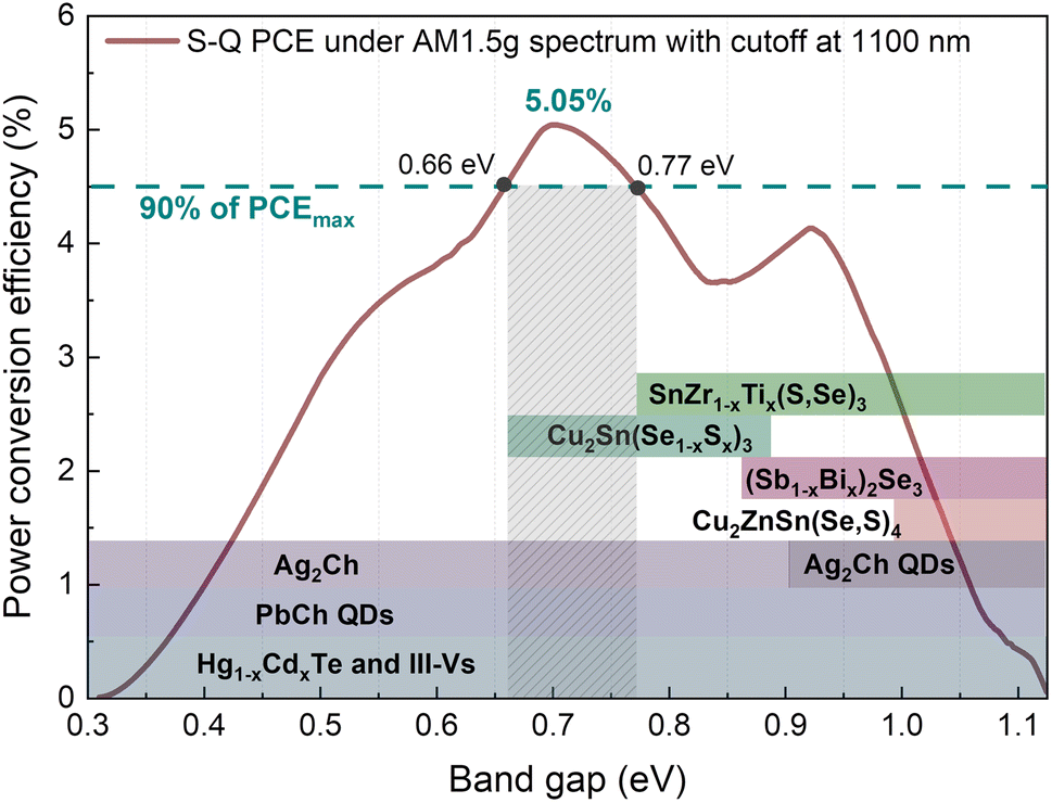 | ||
| Fig. 1 Power conversion efficiency of the solar cell as a function of the absorber's band gap. Calculated following Shockley–Queisser formulation under AM1.5G solar spectrum with a cutoff at 1100 nm (below c-Si absorption edge). Coloured sections indicate the range of achievable band gaps of each material/alloy. | ||
Among technologies that employ low-cost synthesis processes, lead chalcogenide quantum dots (PbCh QDs) due to the quantum confinement effect also offer a very wide range of modifiable absorption edge (Fig. 1).10 It is one of the most developed infrared solar cell technologies that has demonstrated working devices under the AM1.5G solar spectrum with a cut off at 1100 nm wavelength, i.e. below c-Si Eg.10,11 Recently, monovalent silver chalcogenides (Ag2Ch) also attracted attention for optoelectronic application in the near-infrared region.12,13 By changing anions from Se to S, the Eg of bulk Ag2Ch can be varied from 0.15 to 0.9 eV (ref. 14) or even higher in the form of QDs (Fig. 1). Although the above stated technologies allow for engineering optimal Eg for the bottom sub-cell, the viability of these technologies is debatable considering long-term, wide-scale deployment and sustainability. Pb is a heavy toxic metal dangerous to humans and wildlife15 and its use is controlled under strict regulations. Ag is a rare precious metal and is highly utilized by other industries and therefore is limited and expensive.16
Alternatively, emerging PV materials based on a more sustainable and earth-abundant composition, also feature Eg tunability by cationic/anionic substitution. A well-studied PV material from the I2-II-IV-VI4 family, known as kesterite, comprises three cations and one anion which allows for a high variety of compositions. However, none of the chemical variations in kesterite family materials can achieve Eg below 0.9 eV.17 A similar situation also applies to another emerging PV material with adjustable Eg below 1 eV – (Sb1−x,Bix)2Se3.18 The lowest Eg of (Sb1−x,Bix)2Se3 alloy before splitting into two phases can be achieved at x = 0.6 resulting in indirect Eg of 0.86 eV. This value is still too high for the bottom sub-cell absorber and is located at the minimum point (Fig. 1). On the other hand, it was demonstrated that Eg in bulk Cu2Sn(Se1−x,Sx)3 can be varied from 0.67 (x = 0) to 0.87 eV (x = 1) which falls right in the optimal region for the bottom sub-cell.19 Although the true Eg of Cu2Sn(Se1−x,Sx)3 is still under discussion,20 the degenerate nature of Cu2SnSe3 semiconducting properties poses a serious limitation for PV application. A very high intrinsic carrier concentration (>1018 cm−3) was reported in undoped Cu2SnSe3 single crystals21 and even higher for thin films.22 The low formation energy of Cu vacancies and metallic nature of secondary phases were proposed as the origin of high carrier concentration found in Cu2SnS3.23 Therefore, despite the suitable spectral range of the Cu2Sn(Se1−x,Sx)3 alloy, the excessive carrier concentration hampers its potential in PVs. In contrast to numerous materials explored for top and middle sub-cells, there is a void of suitable materials for bottom sub-cell application, especially when the sustainability aspect is taken into account.
Recently, because of the environmentally benign chemical composition and high thermodynamic stability, chalcogenides with a stoichiometry of ABX3 have drawn attention as highly promising sustainable PV materials.24 Specifically, chalcogenide perovskites such as BaZrS3 have raised the highest community interest.25 However, chalcogenide perovskites are wide Eg (>1.6 eV) semiconductors and are therefore typically aimed for application as the top sub-cell. Contrarily, ABX3 chalcogenides with a non-perovskite crystal structure were theoretically predicted to be narrow Eg semiconductors.26 We demonstrated that SnZrSe3 with a non-perovskite structure is a narrow Eg semiconductor with an absorption edge located at ∼1.1 eV.27 Although the Eg of SnZrSe3 is too high for the bottom sub-cell absorber, a low initial value of Eg opens up a possibility to reduce it through cationic substitution. Therefore, our work aims to expand the horizon of materials suitable for infrared solar cell application by studying the optical and electrical properties of Sn(Zr1−xTix)Se3 alloy.
In this work, we synthesized a series of Sn(Zr1−xTix)Se3 samples with different Ti/Zr ratios by solid-state reaction in the 680–750 °C temperature range. Single crystals were also grown using a transport agent in the same setup as powder samples. The structural, optical, and electrical properties of crystals and powders were characterized. We found that Sn(Zr1−xTix)Se3 crystallized in an orthorhombic needle-like phase from x = 0 to x = 0.44. Substitution of Zr with Ti resulted in the redshift of the absorption edge up to 0.78 eV. Additionally, we determined that optical transitions in Sn(Zr1−xTix)Se3 were direct and that the introduction of Ti enhanced the absorption coefficient. A photodetector based on a Ti-rich Sn(Zr,Ti)Se3 single crystal demonstrated a clear photo response in the short wavelength infrared region. In summary, we found that Sn(Zr,Ti)Se3 is a direct Eg semiconductor and its absorption edge can be tuned for application in the infrared region. This makes Sn(Zr,Ti)Se3 a promising absorber material for bottom sub-cell application.
Experimental section
Sn(Zr1−xTix)Se3 samples were synthesized via solid state reaction. The summary of precursor and as-grown sample chemical compositions and synthesis conditions are presented in Table 1. Additional samples were synthesized in the form of single crystals under similar conditions presented in Table 1. We found that there was no significant dependence in Sn(Zr1−xTix)Se3 crystal quality or composition from the top annealing temperatures used in this work, but it affected the yield of Sn(Zr1−xTix)Se3 phase and overall phase composition of the final product. The presence of a higher Ti concentration in the precursor led to a decrease in the yield of the pure Sn(Zr1−xTix)Se3 phase.| Sample name | Ti/(Zr + Ti)a | Ti/(Zr + Ti)b | T 1,c °C | R 1,c °C min−1 | t 1,c h | T 2, °C | R 2, °C min−1 |
|---|---|---|---|---|---|---|---|
| a Molar ratio of Ti to Zr in the precursor by weighted mass. b Molar ratio of Ti to Zr in the single-phase Sn(Zr1−xTix)Se3 powder measured by EDX. c T 1(2), R1(2), t1(2) – temperature, ramp and duration in the first(second) stages of the annealing process. | |||||||
| A0 | 0.0 | 0.0 | 700 | 3.24 | 59 | 500 | 0.11 |
| A1 | 0.08 | 0.094 | 730 | 2.96 | 24 | 600 | 0.03 |
| A2 | 0.15 | 0.20 | 725 | 2.94 | 82 | 600 | 0.21 |
| A3 | 0.3 | 0.27 | 730 | 2.96 | 16 | 550 | 0.04 |
| A4 | 0.4 | 0.37 | 710 | 2.88 | 10 | 600 | 0.03 |
| A5 | 0.5 | 0.45 | 710 | 2.88 | 10 | 600 | 0.03 |
| A6 | 0.6 | 0.42 | 710 | 2.88 | 10 | 600 | 0.03 |
| A7 | 0.7 | N/A | 625 | 2.52 | 38 | 500 | 0.52 |
| A8 | 0.8 | N/A | 730 | 2.96 | 48 | 550 | 0.03 |
| A9 | 0.9 | N/A | 710 | 2.88 | 56 | 600 | 0.37 |
| A10 | 1.0 | N/A | 710 | 2.88 | 70 | 550 | 0.17 |
Samples for solid state synthesis were prepared in the following way: elemental precursors Sn (99.995%, AlfaAesar, −100 mesh), Zr (99.5% STREM Chemicals, −50 mesh), Ti (99.99%, AlfaAesar, −325 mesh), Se (99.999%, AlfaAesar, −200 mesh) and SnI2 (99.99%, SigmaAldrich, −10 mesh) were weighed in a glove box and inserted into the quartz ampoules (inner diameter – 8 mm, outer – 10 mm, length – 150 mm). In the precursors, the molar ratio of cations A to B was kept close to 1, whereas the anion to cation ratio was close to 3![[thin space (1/6-em)]](https://www.rsc.org/images/entities/char_2009.gif) :2. The final weight of the precursors was 0.5 g. Ampoules were capped and taken outside the glovebox. Before the sealing, ampoules were degassed for 30 min under a ∼2 Pa vacuum and then flame-sealed using a propane and oxygen gas mixture. The sealed ampoule length was 60–80 mm. For the crystallization step, samples were placed in the 3-zone tube furnace in a horizontal position and annealed under the conditions listed in Table 1. After annealing, crystals of various shapes and forms were present inside the ampoule indicating that multiple phases were formed. To obtain and study single-phase Sn(Zr1−xTix)Se3 powder properties, large needle-shaped crystals were collected from the ampoule walls and ground with a mortar and pestle. Note that for samples A7–A10 no such crystals were formed and therefore no single-phase powder could be obtained from these batches. The following outcome will be discussed later in the Results section.
:2. The final weight of the precursors was 0.5 g. Ampoules were capped and taken outside the glovebox. Before the sealing, ampoules were degassed for 30 min under a ∼2 Pa vacuum and then flame-sealed using a propane and oxygen gas mixture. The sealed ampoule length was 60–80 mm. For the crystallization step, samples were placed in the 3-zone tube furnace in a horizontal position and annealed under the conditions listed in Table 1. After annealing, crystals of various shapes and forms were present inside the ampoule indicating that multiple phases were formed. To obtain and study single-phase Sn(Zr1−xTix)Se3 powder properties, large needle-shaped crystals were collected from the ampoule walls and ground with a mortar and pestle. Note that for samples A7–A10 no such crystals were formed and therefore no single-phase powder could be obtained from these batches. The following outcome will be discussed later in the Results section.
Phase composition and crystallinity were studied using a SmartLab Rigaku diffractometer with a 9 kW rotating Cu anode in Bragg–Brentano geometry. Diffractograms were recorded from 10 to 60 2θ degrees with a scan step of 0.01° using a linear D/tex ultra detector. Lattice parameters were calculated by fitting a full diffractogram based on the decomposition method and using PDXL software to perform calculations. SnZrSe3 CIF file27 was used as the model structure.
Scanning Electron Microscope (SEM) images were taken using a Helios Nanolab 650 equipped with a field emission gun. Chemical composition was recorded using an energy dispersive spectrometer (Oxford Instruments) embedded in a SEM. Before composition measurements, the Cu plate was used for detector intensity and position calibration and measurements were done at 20 kV and an integration time of 30–45 s per point.
Diffuse reflectance was measured using a Shimadzu UV-3600 two-beam spectrometer equipped with an MPC-3100 multi-purpose compartment. Samples were placed in a 60 mm integrating sphere and a barium sulphate and aluminium mirror were used for spectrum calibration.
Spectroscopic ellipsometry (SE) was used to measure the optical response of samples at room temperature. Measurements were conducted using an RC2 dual rotating-compensator ellipsometer (J. A. Woollam, Co., Inc.) with a 100 μm beam diameter and an incident angle of 55–75° within the spectral range of 0.73–6 eV. To determine the dielectric function of the samples, b-splines were applied28 within the framework of the semi-infinite substrate assuming an isotropic optical response. The absorption coefficient was calculated using the dielectric function determined from SE measurements.
Single crystal samples were used for temperature-dependent electrical current–voltage (J–V) measurements and were recorded using a Keithley 6487 picoammeter/voltage source. Crystals with carbon electrodes were attached to the cold finger and then placed in a closed helium cycle cryostat (Janis CCS-100/204). Temperature was controlled via a digital temperature controller. J–V was measured from 300 to 100 K with either 10 K or 20 K temperature step size. Once the set temperature was reached on the thermocouple, it was left for 2–3 min for the temperature to equalize on the sample.
To test the photo activity of the samples, a needle-shaped crystal was cross-placed on the interdigitated Pt electrodes (ED-IDE3-Pt, 5/5 μm of electrode/gap, Micrux Tech). A slight pressure was applied on the crystal to force it into physical contact with the electrode surface. Contact was confirmed by obtaining a finite resistance between interdigitated electrodes. To measure a transient photocurrent, the sample was excited with a femtosecond laser pulse from the glass side. The excitation wavelength was selected via a collinear optical parametric amplifier (Orpheus PO15F2L, Light Conversion Ltd) which was pumped by a high repetition rate (50 kHz) femtosecond Yb:KGW laser system (Pharos 10-600-PP, Light Conversion Ltd) producing 1030 nm wavelength and 230 fs duration laser pulses. A much lower repetition rate was required to avoid overheating of the sample, therefore the laser pulse repetition rate was set to 5 Hz by using a pulse picker. To extract the photo-generated current, the electric pulse with a duration of 30 μs and 3 V amplitude was applied on the sample by using an arbitrary function generator (Tektronix AFG2021, Tektronix Ltd) synchronized with the pulse picker. The electric pulse was timed at about 15 μs ahead of the laser pulse. The schematic representation of the measurement is shown in Fig. S9, ESI.† Current readings were recorded with an oscilloscope (Siglent SDS1104X-E, Siglent Tech) by measuring the voltage drop on a 1.5 kΩ resistor (that corresponds to approximately 10% of the sample resistance), connected in series with the sample.
Results and discussion
Structural properties of Sn(Zr1−xTix)Se3
A2+B4+X2−3 (X = Se, S) compounds are commonly found in one of the three crystalline phases: (i) distorted perovskite (orthorhombic), (ii) needle-like (orthorhombic) and (iii) BaNiO3-type (hexagonal).29 By analysing the XRD patterns of selectively collected Sn(Zr1−xTix)Se3 samples, we found that all peaks matched well with the reflections from orthorhombic SnZrSe3 in the needle-like phase (Fig. 2a).27 Note that some impurity phases were also detected which originated as byproducts of solid state reaction. However, their quantity was very low and did not influence phase analysis or the calculation of lattice parameters [Fig. S1 and Table S1, ESI†]. Upon the increase in the Ti/Zr ratio, a gradual shift towards higher 2θ angles of all XRD peaks was observed (Fig. 2a and S2a, ESI†). The systematic shift of all XRD peaks indicated that Ti was incorporated in the lattice and it substituted isovalent Zr. Because the ionic radius of Ti is 16% smaller than that of the Zr ion, all crystal lattice parameters diminished with increasing Ti concentration (Fig. 2b). Lattice parameters were calculated by fitting whole XRD patterns and were found to depend linearly on the Ti/Zr ratio (Fig. 2b), therefore were in accordance with Vegard's law. The linear dependence of lattice parameters with respect to Ti quantity was observed up to 0.44 Ti/(Zr + Ti) ratio. Despite the increased Ti amount in the precursors (samples A7 to A10, Table 1), we did not observe Sn(Zr1−xTix)Se3 with a higher Ti/Zr ratio. XRD patterns of the full powder samples (not selectively collected) synthesized using precursors with a Ti/Zr ratio of 0.8, 0.9 and 1.0 are presented in Fig. 2c. In contrast to sample series A1–A6, no XRD peaks were found to match the reflections of Sn(Zr,Ti)Se3 in a needle-like phase. Instead, binary selenide phases such as ZrSe3 (PDF# 00-036-1338), SnSe2 (PDF# 01-089-2939), SnSe (PDF# 01-081-9463) and TiSe2 (PDF# 04-003-1758) were identified. In all three samples, TiSe2 and SnSe2 were found in the highest quantities which also was confirmed by elemental mapping analysis of the sample A10. Many grains with chemical composition representative of SnSe2 and TiSe2 were found (Fig. 2d). We also identified grains/domains where all three elements (Sn, Ti, Se) were present (Fig. 2d, spot b). In the XRD patterns, many of the diffraction peaks could not be assigned to any known phase as well (Fig. 2c, asterisks). This implied that the unknown phase of Sn–Ti–Se could exist, similarly, as it was reported for the Sn–Ti–S system: Sn1.2Ti0.8S3 in a needle-like phase30 and (SnS)1.2(TiS2) in a misfit phase.31 However, by analysing the chemical composition of multiple grains/domains comprising Sn, Ti and Se in sample A10, we did not find the composition that would be typical or representative of A1.2B0.8X3 or (AX)1.2(BX2) stoichiometry (Fig. S2b, ESI†). This suggested that when the elemental ratio in the precursor was 1:1:3, no stable SnTiSe3 compound was formed. It is, however, possible that Sn–Ti–Se crystallized into a ternary phase with a different than 1:1:3 composition, but a more detailed investigation of this possible structure is beyond the scope of this study. In summary, we found that the miscibility region of Sn(Zr1−xTix)Se3 alloy in a needle-like phase with octahedral geometry was from x = 0 to x = 0.44. This indicated the compositional region where the Eg of Sn(Zr1−xTix)Se3 can be modulated and is devoid of secondary phases.
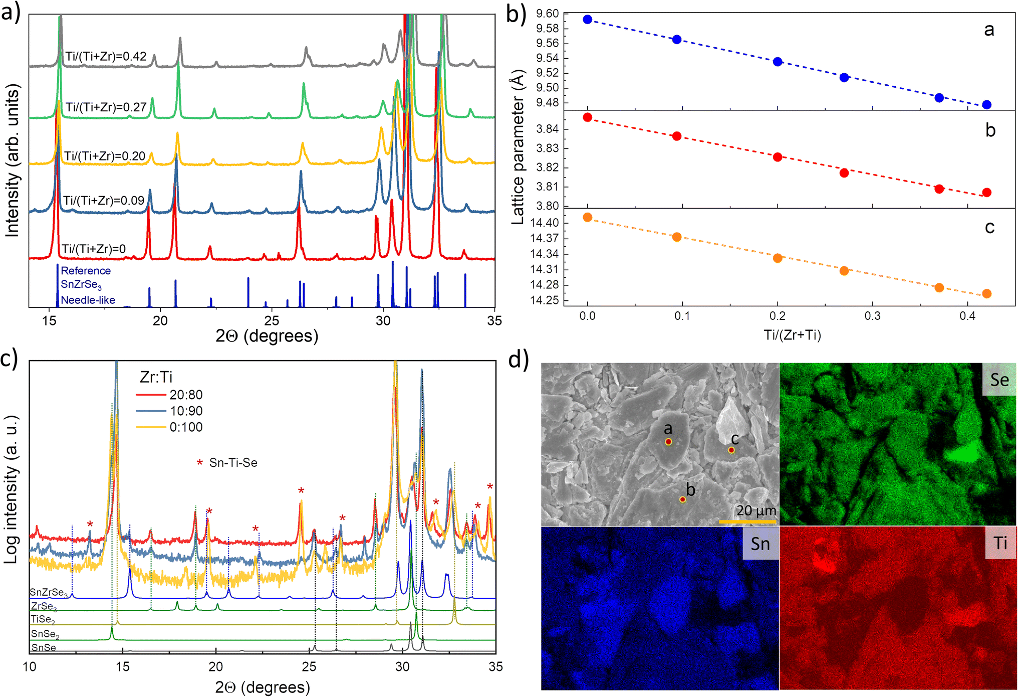 | ||
| Fig. 2 (a) XRD patterns of selectively collected Sn(Zr1−xTix)Se3 powder samples with different Ti/Zr ratios. Peak positions for reference SnZrSe3 in the needle-like phase was taken from single-crystal data in ref. 27. (b) Calculated lattice parameters of Sn(Zr1−xTix)Se3 alloys in the needle-like phase as a function of Ti/Zr ratio. (c) XRD patterns of full Sn(Zr1−xTix)Se3 powder sample synthesized from precursors with Ti concentration higher than 0.8. (d) SEM surface image (top left) and elemental maps of sample A10 in powder form. Coloured images reflect the abundance of elements indicated in the top left corner. Measured composition in spots a, b and c were SnSe2, Sn0.72Ti1.11Se3 and Sn0.08Ti0.85Se2 respectively. | ||
The crystalline phases of ABX3 chalcogenides (X = S, Se) can also be grouped according to the type of octahedral BX6 connectivity: through (i) corner (distorted perovskite), (ii) edge (needle-like) or (iii) face (BaNiO3-type). Most of the A2+B4+X2−3 chalcogenides adopt structures with an edge or face-sharing octahedral geometry and very few with a corner-sharing one.24,32 To support a corner-sharing geometry, the ionic radii (r) of cations and anion must be in specific ratios and this requirement is known as the Goldschmidt tolerance factor.33 While many oxide compounds meet the r conditions for corner-sharing configuration, because of the much larger rX as compared to rO, crystalline structures rearrange to form an edge or face-sharing BX6 octahedral geometry in ABX3 chalcogenides. In extreme cases, when the octahedral factor (μ = rB/rX) becomes very small, the lattice tends to reduce B-site coordination.34 For the case of Sn(Zr1−xTix)Se3 alloy, rX is large and kept constant whereas rB (taken as a weighted sum of rZr and rTi) becomes gradually smaller by increasing the Ti/Zr ratio. At a certain Ti concentration, because of the decreased rB, μ reaches the limit where octahedral edge-sharing geometry in the ternary compound cannot be sustained. Consequently, the structure breaks down into binary compounds or other ternary phases with reduced B-site coordination. Based on the experimental results, the structural stability limit of the edge-sharing phase in Sn(Zr1−xTix)Se3 is reached when the Ti/(Zr + Ti) ratio is ∼0.44. Taking ionic radii of B and X from Shannon's work35 and considering B cation coordination number VI, μ = 0.338 when Ti/(Zr + Ti) = 0.44. In the case of the sulphides, SnTiS3 does adopt an edge-sharing crystalline structure,30 however at the expense of severe deviation from 1:1:3 stoichiometry (Sn1.2Ti0.8S3), and it also required high pressure synthesis conditions. For stoichiometric SnTiS3μ = 0.329, which is below the μ limit we calculated for selenides. However, if we consider that a fraction (0.2) of Sn atoms occupy the Ti site in the Sn1.2Ti0.8S3 structure with a 4+ state, μ becomes 0.338. Note that now we arrive at the same μ value for both materials. This μ value, therefore, can be regarded as the lower stability limit for ABX3 chalcogenides with B-site in octahedral coordination. For Ti and Se octahedral μ = 0.31 and thus is below the suggested stability limit. To the best of our knowledge, there is no stable ATiSe3 (A = Ca, Sr, Ba, Sn, Pb, Eu) structure with the Ti-site in octahedral coordination. Arguably there is one report on the formation of BaTiSe3 in a face-sharing structure36 and there is an entry in the ICSD database which was based on the same publication. However, structural data are not very reliable (marked as low-quality), and this compound has not been synthesized repeatedly which questions the stability of the BaTiSe3 phase or its original structure.
Using the derived stability limit, one can calculate how much Ti can be incorporated in SnZrS3 with an edge-sharing octahedral geometry. Because rS is smaller than rSe, we would expect to be able to introduce higher concentrations of Ti than in the selenide counterpart. Taking μ = 0.338 as the limit, the structure should be stable up to 0.85 Ti/(Ti + Zr) ratio. We synthesized a range of Sn(Zr1−xTix)S3 alloys and carried out preliminary studies where we found crystals with a Ti/(Zr + Ti) ratio reaching 0.72 (Fig. S3, ESI†). This is already a much higher concentration of incorporated Ti than was possible in the selenide compounds. Knowing the compositional limit of the stable Sn(Zr1−xTix)S3 phase one can predict the range of achievable Eg in this compound. In our discussion, we did not consider the impact of cation A because in the materials under this study, cation A was the same. However, we acknowledge that the size and nature of cation A will also have an influence on the stability of the ABX3 compound with octahedral B-site coordination.
Optical properties of Sn(Zr1−xTix)Se3 alloy
To estimate the optical absorption edge and its relation to the chemical composition, diffuse reflectance was measured for the single-phase Sn(Zr1−xTix)Se3 powder samples. The Kubelka–Munk equation was used to calculate apparent absorption as a function of the incident photon energy.37 The calculated apparent absorption spectra of Sn(Zr1−xTix)Se3 samples are depicted in Fig. 3a, and the absorption edges determined by analysing the linear slope of a Tauc plot are shown in Fig. 3b. When the quantity of Ti in the Sn(Zr1−xTix)Se3 increased, the absorption edge shifted towards lower energies (Fig. 3b). The Eg was calculated assuming direct optical transition and was found to be in the 0.78–1.07 eV range (Fig. 3c). Clearly, the substitution of Zr with Ti led to the decrease of the Eg and the lowest achieved value was 0.78 ± 0.01 eV which is near the optimal Eg required for the bottom sub-cell (Fig. 1).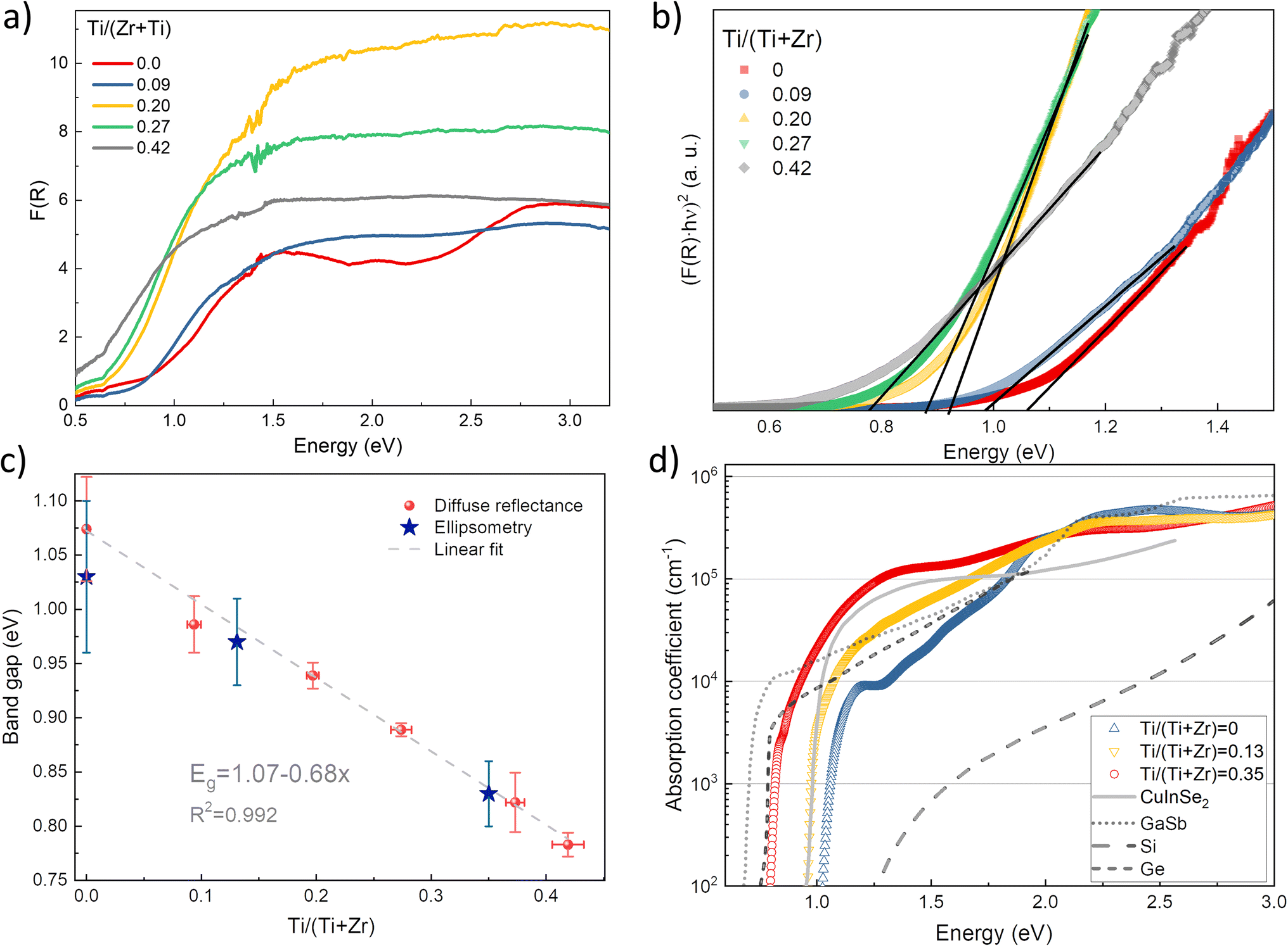 | ||
| Fig. 3 (a) Calculated apparent absorption of Sn(Zr1−xTix)Se3 powder samples with different Ti/Zr ratios. (b) Tauc plot of the absorption edge of Sn(Zr1−xTix)Se3 powder samples with different Ti/Zr ratios. Direct optical transitions were considered. (c) Sn(Zr1−xTix)Se3 band gap as a function of Ti/Zr ratio measured by diffuse reflectance from powder samples and by spectroscopic ellipsometry from single crystals. Y-axis error was estimated by fitting the linear region in Tauc plot with least squares method. X-axis error was estimated by calculating standard deviation of Ti/(Zr + Ti) ratio derived from atomic composition measurements over 5 points. (d) Calculated absorption coefficient of Sn(Zr1−xTix)Se3 single crystals with different Ti/Zr ratios. The absorption coefficient of CuInSe2, GaSb and Si was taken from ref. 40–42. | ||
For application in solar cells, it is also essential to determine the material's capability to absorb light radiation. For this reason, the absorption coefficient of representative samples (single crystals) was studied using SE. Because of the very small crystal size (crystal width <250 μm, Fig. S4, ESI†), ellipsometry measurements were carried out only along the main needle direction with a focused beam and at a narrow range of incident angles. The optical constants were determined by assuming isotropic optical response, but this may not be entirely accurate due to the quasi-one-dimensional Sn(Zr1−xTix)Se3 structure. However, this rough approximation closely aligned with theoretical calculations, suggesting that there are no significant differences in dielectric function along the three crystallographic directions.38 As a result, we believe that such an approximation is valid for estimating the absorption coefficient (α) of Sn(Zr1−xTix)Se3 within a reasonable margin of error.
Three crystals were studied: Ti-free SnZrSe3, Sn(Zr0.87Ti0.13)Se3 and Ti-rich Sn(Zr0.65Ti0.35)Se3. As seen in Fig. 3d, the absorption edge of SnZrSe3 was located at around 1.0 eV and rose sharply up to 8 × 103 cm−1, and then the slope of α flattened continuing to increase up to 3 × 105 cm−1 before reaching the plateau. The steep slope of α near the absorption edge strongly suggested that SnZrSe3 is a direct gap semiconductor in stark contrast to Si (Fig. 3d). However, a strongly absorbing region (α > 104 cm−1) is achieved for photons with an energy higher than 1.3 eV resulting in an absorption onset (defined as the difference between Eg and energy at which α > 104 cm−1) of around 0.3 eV. This observation is in reasonable agreement with theoretical predictions stating that the absorption onset in the needle-like phase SnZrSe3 is about 0.5 eV.38 Interestengly, a significant absorption onset (>0.5 eV) was predicted theoretically26 and confirmed experimentally39 also in other ABX3 compounds that crystalise in a needle-like phase, for instance α-SrZrS3. In contrast, α in samples with moderate and high Ti concentrations increased more steeply and reached 104 cm−1 at 1.07 and 0.93 eV photon energies, respectively. That represented the absorption onset of only about 0.1 eV in both samples. The magnitude and steepness of α was comparable with a well-known material (CuInSe2) used in high-efficiency thin film solar cells,40 and was higher than that of classical semiconductors used as bottom sub-cell absorbers in multijunction devices (Ge,41 GaSb42) (Fig. 3d). The calculated Eg for SnZrSe3, Sn(Zr0.87Ti0.13)Se3 and Sn(Zr0.65Ti0.35)Se3 crystals from ellipsometry measurements were in good agreement with results obtained from diffused reflectance measurements (Fig. 3c). Note that a larger difference was found in case of SnZrSe3 likely because of higher absorption onset than in Sn(Zr1−xTix)Se3 samples.
The incorporation of Ti in the SnZrSe3 structure did not change the optical transition nature but increased the absorption coefficient and reduced the Eg. These effects originated from the modification in the band structure upon Ti inclusion. In the ABX3 compounds where B = transition metal, X = Se, S, regardless of the equilibrium crystal structure, the primary contribution to the density of states at conduction and valence bands' edges arises from d orbitals of cation B and p orbitals of anion, respectively.43–45 Substitution of cation B thus will affect the characteristics of the conduction band and in turn the optical properties. Because the energy of Ti 3d orbitals lays deeper than that of Zr 4d orbitals, the incorporation of the Ti results in the downward shift of the conduction band and therefore the narrowing of the Eg. At the same time, when moving up in the periodic table, the d orbitals of transition metals contract because of the decrease in principal quantum number and therefore become more localized. This implies that by substituting Zr (4d) with Ti (3d), more localized orbitals contribute to the conduction band edge making it less dispersive. The less dispersive character of the conduction band edge leads to the higher joint density of states and therefore increased probability of optical transition.46 Therefore we observed a higher absorption coefficient for compounds containing Ti. Because of the same reasoning, a steeper rise of α is observed in TiO2 as compared to ZrO2 (Fig. S5, ESI†). In summary, alloying SnZrSe3 with Ti not only shifted the absorption edge towards the infrared region, but also increased the absorption coefficient which was comparable with that of the well-established PV materials used in thin film solar cells.
Electrical properties of Sn(Zr1−xTix)Se3 alloy
Alloying SnZrSe3 with Ti will also have an impact on electrical properties. Previously, we determined that for undoped SnZrSe3 conductivity type was dependent on the Sn/Zr ratio and room temperature (RT) resistivity varied in the 104–105 Ω cm range.27 In this work, the electrical properties of the Sn(Zr1−xTix)Se3 were studied by measuring RT resistivity and temperature-dependent current–voltage (J–V) characteristics of crystals. Needle-shaped crystals were attached to a polyimide-covered metallic holder and carbon paste was applied on the crystal ends that acted as contacts (Fig. 4a, inset). Carbon-paste electrodes ensured ohmic contact behaviour as evidenced by a linear J–V relationship in the entire temperature range for samples with various Ti/Zr ratios (Fig. S6, ESI†).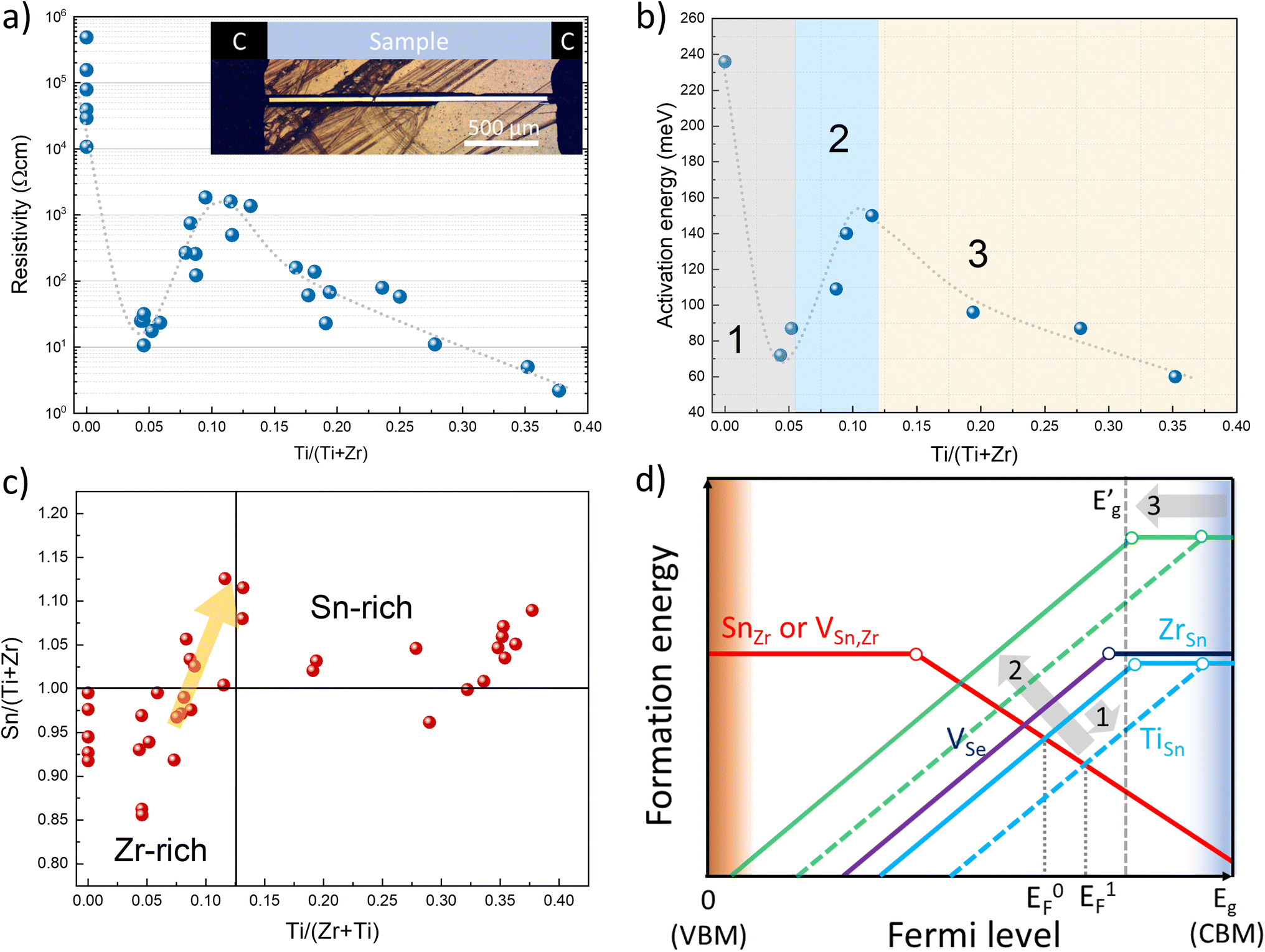 | ||
| Fig. 4 (a) Room temperature resistivity as a function of Ti/(Ti + Zr) ratio measured in Sn(Zr1−xTix)Se3 single crystals. Inset: optical photograph of an Sn(Zr1−xTix)Se3 single crystal with carbon electrodes. (b) Activation energy calculated from temperature dependent conductivity as a function of Ti/(Ti + Zr) ratio. Note that the grey dashed curve is an arbitrary fit that serves as a guide. (c) Sn ratio to (Zr + Ti) as a function of Ti/(Ti + Zr) measured by EDS in randomly selected Sn(Zr1−xTix)Se3 single crystals. (d) Schematic representation of formation energies of intrinsic point defects with respect to the Fermi level in Sn(Zr1−xTix)Se3. | ||
First, to identify the majority carrier type, Sn(Zr1−xTix)Se3 crystals were measured by the hot point probe (HPP) method. For samples with x > 0, we observed a significant positive increase in HPP response (Fig. S7a, ESI†). This confirmed that n-type conductivity was dominant in Sn(Zr1−xTix)Se3 alloy regardless of the Ti concentration. RT resistivity measurements of samples with various Ti/Zr ratios revealed unexpected electrical behaviour. In the Ti-free crystals, the RT resistivity depended on the Sn/Zr ratio and varied in the 104–7 × 10⁵ Ω cm range. Upon a small incorporation of Ti, resistivity of the crystals dropped almost four orders of magnitude (Fig. 4a). With a further increase in Ti/Zr ratio, resistivity started to rise reaching the maximum value of about 103 Ω cm which was then followed by a gradual decrease to 2 × 100 Ω cm at the highest Ti concentration (Fig. 4a). To get a deeper insight into such uncharacteristic electrical behaviour, we estimated the activation energy (Ea) of defects contributing to the conductivity. This was achieved by plotting conductivity as a function of reciprocal temperature and calculating the slope in the linear region (Fig. S7b, ESI†). It was found that the dependence of Ea on Ti concentration had a very similar behaviour as resistivity (Fig. 4b). This strongly suggested that conductivity in Sn(Zr1−xTix)Se3 was governed by the formation of various intrinsic point defects rather than extrinsic. Having extrinsic doping would lead to a constant gradual change of Ea in positive correlation with Eg narrowing throughout the whole compositional range.
The observed electrical behaviour in relation to Ti composition can be divided into three regions: (1) a sudden drop of Ea at low Ti concentration; (2) an increase in Ea with increasing Ti/Zr ratio up to 0.12 and (3) a gradual decrease of Ea with further increase in Ti/Zr ratio (Fig. 4b). We already inferred that free carrier concentration depended solely on intrinsic point defects. Therefore, the chemical composition will be a deciding factor for the electrical behaviour in Sn(Zr1−xTix)Se3. To get a better understanding of point defects and their formation dynamics in Sn(Zr1−xTix)Se3, one has to identify prevalent donor and acceptor type defects that are typical of A2+B4+X2−3 (X = Se, S) materials. Data on defects in ABX3 (X = Se, S) compounds are very scarce in the literature, hence we rely on the available defect chemistry analysis reported for BaZrS3.47 BaZrS3 is from the same ABX3 material family and shares the same structural building block as octahedral Sn(Zr1−xTix)Se3–BX6 (X = Se, S). Therefore, the defect formation tendencies described for BaZrS3 to some extent can be extrapolated to Sn(Zr1−xTix)Se3.
In BaZrS3, under stoichiometric composition, the lowest formation energy of donor type defects was calculated for antisite defects where cation B replaces cation A (BA), and for chalcogenide vacancy (VX).47 The lowest formation energy of acceptor type defects was calculated for antisite defect where cation A replaces B (AB) and cations' A and B vacancies (VA, VB). Experimental results showed that Sn(Zr1−xTix)Se3 is more likely to show n-type conductivity than p-type which is also the case for BaZrS3.48 For this reason, we conclude that ZrSn and VSe have the lowest formation energies and therefore are prevalent donor defects in Sn(Zr1−xTix)Se3. By measuring the Ea of n-type SnZrSe3 crystals we found that it varied in the 240–280 meV range (Fig. S8a, ESI†). Based on this finding, we infer that both ZrSn and VSe are present in high concentrations and have comparable ionization potentials (Ei). Under equilibrium conditions for Ti-free SnZrSe3, we thus expect the Fermi level to be positioned slightly towards the conduction band minimum (CBM) as shown in Fig. 4d (EF0). When Ti was incorporated into the lattice, it replaced the Zr site and this in turn led to the formation of TiSn antisite defects. However, TiSn defects had a much smaller Ei as evidenced by a sudden drop in Ea for samples with low Ti concentration (Fig. 4b). Smaller Ei meant that more electrons were thermally excited to the conduction band and the Fermi level shifted towards CBM (Fig. 4d, EF1). Note that Eg narrowing could not account for a sudden drop of Ea which was in the 110–190 meV range as compared to only a 40–60 meV reduction in Eg (Fig. 3c). In the second region, the rise in Ea with increasing Ti/Zr ratio was associated with the changes in Sn(Zr1−xTix)Se3 stoichiometry. By measuring the chemical composition of more than 35 randomly selected Sn(Zr1−xTix)Se3 single crystals from various batches, we found that there was a positive correlation between Ti and Sn quantities. When a higher amount of Ti was introduced in the precursors, we observed that the as-grown crystals from slightly cation B-rich composition became more cation A-rich (Fig. 4c). The turning point occurred at about 0.07 Ti/(Ti + Zr) ratio and reached the maximum at 0.12. The shift of stoichiometry from Sn-poor to Sn-rich consequently had a strong effect on the formation of Zr(Ti)Sn antisite defects. Initially prevalent Zr(Ti)Sn defects became less favourable therefore their formation energy increased (Fig. 4d, green lines) leaving the VSe as the dominant donor defect. The concentration of VSe increased as samples became more Sn-rich and because VSe are deep defects, Ea increased. In the final region, a further increase of Ti concentration resulted in a more notable downward shift of CBM, as discussed in the Optical properties section. As a result, the Ei of VSe gradually decreased causing VSe to become shallow defects (Fig. 4d,  ) and therefore leading to a significant increase in free carrier concentration.
This tentative model explains the behaviour of electrical conductivity in Sn(Zr1−xTix)Se3, but we acknowledge that contribution from other types of defect or defect complexes cannot be completely ruled out because we relied on defect chemistry analysis for BaZrS3 which crystallizes in the distorted perovskite structure. Additionally, the estimate on carrier mobility is needed to confirm whether there is an excessive carrier concentration in the sample with a high Ti concentration. High carrier concentration could potentially limit the application of Sn(Zr1−xTix)Se3 in PVs similarly as for Cu2SnSe3.
To showcase the photo activity of the Sn(Zr1−xTix)Se3 crystals in the short wavelength infrared region (SWIR), we set up the photocurrent measurements using single Sn(Zr,Ti)Se3 crystals with a Ti/(Zr + Ti) ratio of 0.37, corresponding to the absorption edge at ∼0.8 eV. To record the photocurrent, the crystal was placed on the interdigitated Pt electrodes (Fig. 5, inset), excited with a laser and then a voltage pulse was applied to extract photo-generated carriers (see the Experimental section and Fig. S9, ESI†). Photocurrent was measured under three excitation wavelengths: 1550 nm (0.8 eV), 1650 nm (0.75 eV) and 1750 nm (0.71 eV). A clear photo response was observed under all three excitation wavelengths (Fig. 5). The strongest signal was obtained under the λ = 1550 nm which was sufficient for the band-to-band carrier generation. Under lower energy excitation, the contribution to photocurrent likely occurred via sub-band absorption by deep defects.49,50 Photocurrent decay was on the order of μs suggesting that the photo-generated carrier lifetime was in the range of hundreds of ns. However, due to very low signal, carrier lifetime could not be calculated accurately. Nevertheless, much higher than 100 ns photo-generated carrier lifetime is essential to achieve high-performance solar cells.51,52 In summary, we demonstrate a proof-of-concept that Sn(Zr,Ti)Se3 with Ti-rich composition is a photo active material in the SWIR region which is imperative for the bottom sub-cell absorber.
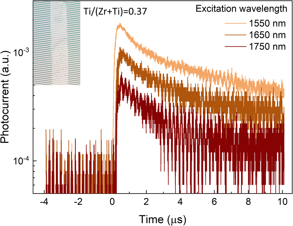 | ||
| Fig. 5 Transient photocurrent measurement in single Sn(Zr0.63Ti0.37)Se3 crystal under various excitation wavelengths. Inset: optical image of the Sn(Zr0.63Ti0.37)Se3 crystal placed on interdigitated Pt electrodes (from the glass side). | ||
The next stage in the progress of infrared solar cells based on ABX3 would be the demonstration of Sn(Zr,Ti)Se3 thin films. Technology, however, is in its very early stage of development and synthesis of ABX3 thin films has been reported only for two compounds thus far: BaZrS3 (ref. 25, 48, 53 and 54) and CaSnS3.55 In both cases, thin films were successfully obtained via a two-step process which includes: (i) deposition of oxide or metallic thin film precursor and (ii) reactive annealing of the precursor under a chalcogen-rich atmosphere. This approach can be potentially applied for formation of Sn(Zr,Ti)Se3 thin films as well. It is noteworthy that O contamination during precursor preparation will be of critical importance. Due to the very high chemical affinity of O with Ti/Zr, it required high temperatures (>800 °C) to substitute O with a chalcogen.53 Such temperatures are not compatible with standard substrates used in photovoltaics but can be mitigated using metallic precursors.25 The two-step synthesis approach involving metallic precursor preparation, therefore, seems to be a viable strategy for formation of Sn(Zr,Ti)Se3 thin films.
Conclusions
In this work, we studied Sn(Zr1−xTix)Se3 alloy which is a member of ABX3 chalcogenide family materials. The goal was to examine the physical properties of Sn(Zr1−xTix)Se3 with various Ti/Zr ratios. We found that Sn(Zr1−xTix)Se3 was stable in a needle-like phase with an edge-sharing BX6 octahedral structure up to x = 0.44. The increasingly higher difference between ionic radii of cation B and anion X upon Ti incorporation resulted in ABX3 structure breakdown into secondary phases. The absorption edge of Sn(Zr1−xTix)Se3 alloy redshifted with increasing Ti concentration and the lowest obtained Eg was 0.78 ± 0.01 eV. This Eg is close to the optimal value to reach maximum PCE for the bottom sub-cell in a c-Si based three junction solar cell. In addition, because of the more localized character of Ti 3d orbitals, the absorption coefficient of Sn(Zr1−xTix)Se3 with x > 0 was higher than in Ti-free and was comparable with other well-established PV absorbers used in thin-film solar cells. The incorporation of Ti had a significant effect on electrical behaviour. Room temperature resistivity decreased by 5 orders of magnitude at the highest Ti/Zr ratio, therefore the control of the chemical composition will play a vital role in avoiding excessive carrier concentration. Finally, by measuring the photo response of Sn(Zr0.63Ti0.37)Se3 in the 0.7–0.8 eV range we demonstrated that Sn(Zr,Ti)Se3 with Ti-rich composition is a photo-active material in the short wavelength infrared region. Optoelectronic properties of Sn(Zr1−xTix)Se3 make it a very interesting material candidate for an infrared solar cell application, but a further demonstration of Sn(Zr1−xTix)Se3 in thin film form is needed to showcase its full potential for PVs.Data availability
Raw and processed data used to prepare figures in the article and ESI are available from the following repository: https://doi.org/10.5281/zenodo.10019524.†Author contributions
R. K. – conceptualization, data curation, formal analysis, funding acquisition, investigation, project administration, resources, supervision, validation, writing original draft; V. P. – investigation; M. F. – investigation, writing – review & editing; A. S. – investigation, validation, writing – review & editing; S. T. – formal analysis, investigation, validation, writing – review & editing; V. J. – investigation, validation; R. J. – resources, writing – review & editing; A. K. – writing – review & editing; K. M. – investigation; M. K. K. – resources, writing – review & editing.Conflicts of interest
There are no conflicts to declare.Acknowledgements
This project has received funding from the European Union's Horizon 2020 research and innovation programme under the Marie Sklodowska-Curie grant agreement No. 895046 (project Chalcogenide-perovskites for infrared photovoltaics [IRPV]). Authors thank S. Lu for providing theoretical calculations of solar cell performance.References
- M. A. Green, E. D. Dunlop, M. Yoshita, N. Kopidakis, K. Bothe, G. Siefer and X. Hao, Prog. Photovolt., 2023, 31, 651–663 CrossRef.
- L. C. Hirst and N. J. Ekins-Daukes, Prog. Photovolt., 2011, 19, 286–293 CrossRef.
- S. P. Bremner, M. Y. Levy and C. B. Honsberg, Prog. Photovolt., 2008, 16, 225–233 CrossRef.
- A. H. Ip, A. Kiani, I. J. Kramer, O. Voznyy, H. F. Movahed, L. Levina, M. M. Adachi, S. Hoogland and E. H. Sargent, ACS Nano, 2015, 9, 8833–8842 CrossRef CAS PubMed.
- J. Liu, J. Qu, T. Kirchartz and J. Song, J. Mater. Chem. A, 2021, 9, 20919–20940 RSC.
- I. Lombardero, M. Ochoa, N. Miyashita, Y. Okada and C. Algora, Prog. Photovolt.s, 2020, 28, 1097–1106 CrossRef CAS.
- J. Tournet, S. Parola, A. Vauthelin, D. M. Cardenes, S. Soresi, F. Martinez, Q. Lu, Y. Cuminal, P. Carrington and J. Décobert, Sol. Energy Mater. Sol. Cells, 2019, 191, 444–450 CrossRef CAS.
- A. Rogalski, Rep. Prog. Phys., 2005, 68, 2267 CrossRef CAS.
- C.-Z. Ning, L. Dou and P. Yang, Nat. Rev. Mater., 2017, 2, 1–14 Search PubMed.
- Y. Xia, S. Liu, K. Wang, X. Yang, L. Lian, Z. Zhang, J. He, G. Liang, S. Wang, M. Tan, H. Song, D. Zhang, J. Gao, J. Tang, M. C. Beard and J. Zhang, Adv. Funct. Mater., 2020, 30, 1907379 CrossRef CAS.
- C. Ge, E. Yang, X. Zhao, C. Yuan, S. Li, C. Dong, Y. Ruan, L. Fu, Y. He and X. Zeng, Small, 2022, 18, 2203677 CrossRef CAS PubMed.
- C. Liao, L. Tang, Y. Li, S. Sun, L. Wang, J. Xu, Y. Jia and Z. Gu, Nanoscale, 2022, 14, 10169–10175 RSC.
- W. Yu, J. Yin, Y. Li, B. Lai, T. Jiang, Y. Li, H. Liu, J. Liu, C. Zhao and S. C. Singh, ACS Appl. Energy Mater., 2019, 2, 2751–2759 CrossRef CAS.
- T. R. Wei, P. Qiu, K. Zhao, X. Shi and L. Chen, Adv. Mater., 2023, 35, 2110236 CrossRef CAS PubMed.
- A. L. Wani, A. Ara and J. A. Usmani, Interdiscip. Toxicol., 3916, 8, 55–64 CrossRef PubMed.
- L. Grandell and A. Thorenz, Renewable Energy, 2014, 69, 157–165 CrossRef CAS.
- W. Gong, T. Tabata, K. Takei, M. Morihama, T. Maeda and T. Wada, Phys. Status Solidi C, 2015, 12, 700–703 CrossRef CAS.
- T. P. Weiss, P. Arnou, M. Melchiorre, M. Guennou, D. Siopa, C. Pauly, I. P. Alonso, P. J. Dale and S. Siebentritt, Phys. Rev. Appl., 2020, 14, 024014 CrossRef CAS.
- T. Nomura, T. Maeda, K. Takei, M. Morihama and T. Wada, Phys. Status Solidi C, 2013, 10, 1093–1097 CrossRef CAS.
- M. R. Pallavolu, A. N. Banerjee, V. R. M. Reddy, S. W. Joo, H. R. Barai and C. Park, Sol. Energy, 2020, 208, 1001–1030 CrossRef CAS.
- G. Marcano, C. Rincón, L. De Chalbaud, D. Bracho and G. S. Pérez, J. Appl. Phys., 2001, 90, 1847–1853 CrossRef CAS.
- G. S. Babu, Y. K. Kumar, Y. B. K. Reddy and V. S. Raja, Mater. Chem. Phys., 2006, 96, 442–446 CrossRef CAS.
- L. L. Baranowski, P. Zawadzki, S. Christensen, D. Nordlund, S. Lany, A. C. Tamboli, L. Gedvilas, D. S. Ginley, W. Tumas and E. S. Toberer, Chem. Mater., 2014, 26, 4951–4959 CrossRef CAS.
- K. V. Sopiha, C. Comparotto, J. A. Márquez and J. J. Scragg, Adv. Opt. Mater., 2022, 10, 2101704 CrossRef CAS.
- C. Comparotto, P. Strom, O. Donzel-Gargand, T. Kubart and J. J. Scragg, ACS Appl. Energy Mater., 2022, 5, 6335–6343 CrossRef CAS.
- Y.-Y. Sun, M. L. Agiorgousis, P. Zhang and S. Zhang, Nano Lett., 2015, 15, 581–585 CrossRef CAS PubMed.
- R. Kondrotas, R. Juskenas, A. Krotkus, V. Pakstas, A. Suchodolskis, A. Mekys, M. Franckevicius, M. Talaikis, K. Muska, X. Li, M. Kauk-Kuusik and V. Kravtsov, Open Research Europe, 2023, 2, 138 Search PubMed.
- B. Johs and J. S. Hale, Phys. Status Solidi A, 2008, 205, 715–719 CrossRef CAS.
- M. Buffiere, D. S. Dhawale and F. El-Mellouhi, Energy Technol., 2019, 7, 1900819 CrossRef CAS.
- K. Suekuni, H. Usui, S. Qiao, K. Hashikuni, T. Hirano, H. Nishiate, C.-H. Lee, K. Kuroki, K. Watanabe and M. Ohtaki, J. Appl. Phys., 2019, 125(17), 175111 CrossRef.
- N. S. Rajput, H. Baik, J.-Y. Lu, S. R. Tamalampudi, R. Sankar, A. Al Ghaferi and M. Chiesa, J. Phys. Chem. C, 2021, 125, 9956–9964 CrossRef CAS.
- D. Tiwari, O. S. Hutter and G. Longo, J. Phys.: Energy, 2021, 3, 034010 CAS.
- V. M. Goldschmidt, Naturwissenschaften, 1926, 14, 477–485 CrossRef CAS.
- M. R. Filip and F. Giustino, Proc. Natl. Acad. Sci. U. S. A., 2018, 115, 5397–5402 CrossRef CAS PubMed.
- R. t. Shannon and C. Prewitt, Acta Crystallogr., Sect. B: Struct. Crystallogr. Cryst. Chem., 1970, 26, 1046–1048 CrossRef CAS.
- L. Aslanov, Russ. J. Inorg. Chem., 1964, 9, 1090–1091 Search PubMed.
- P. Kubelka, Z. Tech. Phys, 1931, 12, 593–601 Search PubMed.
- N. B. Bellil, F. Litimein, H. Khachai, R. Khenata, A. Abdiche, E. Güler, R. Ahmed, A. Bouhemadou, S. B. Omran and J. M. Khalifeh, Mater. Today Commun., 2021, 27, 102427 CrossRef.
- S. Niu, H. Huyan, Y. Liu, M. Yeung, K. Ye, L. Blankemeier, T. Orvis, D. Sarkar, D. J. Singh and R. Kapadia, arXiv, 2018, preprint, arXiv:1804.09362, DOI:10.48550/arXiv.1804.09362.
- J. Jaffe and A. Zunger, Phys. Rev. B: Condens. Matter Mater. Phys., 1984, 29, 1882 CrossRef CAS.
- W. Dash and R. Newman, Phys. Rev., 1955, 99, 1151 CrossRef CAS.
- M. Muñoz, K. Wei, F. H. Pollak, J. Freeouf and G. Charache, Phys. Rev. B: Condens. Matter Mater. Phys., 1999, 60, 8105 CrossRef.
- K. Hanzawa, S. Iimura, H. Hiramatsu and H. Hosono, J. Am. Chem. Soc., 2019, 141, 5343–5349 CrossRef CAS PubMed.
- S. Niu, G. Joe, H. Zhao, Y. Zhou, T. Orvis, H. Huyan, J. Salman, K. Mahalingam, B. Urwin and J. Wu, Nat. Photonics, 2018, 12, 392–396 CrossRef CAS.
- N. A. Moroz, C. Bauer, L. Williams, A. Olvera, J. Casamento, A. A. Page, T. P. Bailey, A. Weiland, S. S. Stoyko and E. Kioupakis, Inorg. Chem., 2018, 57, 7402–7411 CrossRef CAS PubMed.
- L. Yu, R. S. Kokenyesi, D. A. Keszler and A. Zunger, Adv. Energy Mater., 2013, 3, 43–48 CrossRef CAS.
- W. Meng, B. Saparov, F. Hong, J. Wang, D. B. Mitzi and Y. Yan, Chem. Mater., 2016, 28, 821–829 CrossRef CAS.
- X. Wei, H. Hui, C. Zhao, C. Deng, M. Han, Z. Yu, A. Sheng, P. Roy, A. Chen and J. Lin, Nano Energy, 2020, 68, 104317 CrossRef CAS.
- K. Li, X. Yang, F. Yang, J. He, G. Zhang, S. Jiang, C. Chen and J. Tang, Mater. Today Electron., 2022, 2, 100011 CrossRef.
- M. Tabbal, T. Kim, D. N. Woolf, B. Shin and M. J. Aziz, Appl. Phys. A: Mater. Sci. Process., 2010, 98, 589–594 CrossRef CAS.
- M. Ochoa, S. C. Yang, S. Nishiwaki, A. N. Tiwari and R. Carron, Adv. Energy Mater., 2022, 12, 2102800 CrossRef CAS.
- J. Tong, Z. Song, D. H. Kim, X. Chen, C. Chen, A. F. Palmstrom, P. F. Ndione, M. O. Reese, S. P. Dunfield and O. G. Reid, Science, 2019, 364, 475–479 CrossRef CAS PubMed.
- J. A. Márquez, M. Rusu, H. Hempel, I. Y. Ahmet, M. Kölbach, I. Simsek, L. Choubrac, G. Gurieva, R. Gunder and S. Schorr, J. Phys. Chem. Lett., 2021, 12, 2148–2153 CrossRef PubMed.
- Z. Yu, X. Wei, Y. Zheng, H. Hui, M. Bian, S. Dhole, J.-H. Seo, Y.-Y. Sun, Q. Jia and S. Zhang, Nano Energy, 2021, 85, 105959 CrossRef CAS.
- H. Shaili, M. Beraich, M. Ouafi, E. mehdi Salmani, R. Essajai, W. Battal, M. Rouchdi, M. h. Taibi, N. Hassanain and A. Mzerd, J. Alloys Compd., 2021, 851, 156790 CrossRef CAS.
Footnote |
| † Electronic supplementary information (ESI) available. See DOI: https://doi.org/10.1039/d3ta05550g |
| This journal is © The Royal Society of Chemistry 2023 |