
Flexible Bi2Te3/PEDOT nanowire sandwich-like films towards high-performance wearable cross-plane thermoelectric generator and temperature sensor array†
Minzhi
Du
ab,
Jianyong
Ouyang
 *bc and
Kun
Zhang
*a
*bc and
Kun
Zhang
*a
aKey Laboratory of Textile Science & Technology (Ministry of Education), College of Textiles, Donghua University, Shanghai 201620, PR China. E-mail: kun.zhang@dhu.edu.cn
bDepartment of Materials Science and Engineering, National University of Singapore, 9 Engineering Drive 1, 117576, Singapore. E-mail: mseoj@nus.edu.sg
cNational University of Singapore (Suzhou) Research Institute, No. 377 Linquan Street, Suzhou Industrial Park, Suzhou, Jiangsu 215123, PR China
First published on 13th June 2023
Abstract
It is of significance to develop high-performance organic/inorganic hybrid thermoelectric (TE) materials for flexible cross-plane TE devices. In this work, we synthesize a flexible and free-standing sandwich-like TE film by depositing Bi2Te3 nanocrystals into a conducting porous PEDOT nanowire scaffold. The mechanically robust Bi2Te3@PEDOT nanowire film exhibits a record Seebeck coefficient of 266.4 μV K−1 with a corresponding power factor of 740.2 μW m−1 K−2 and a zT value of 0.27 at room temperature. Afterwards, we build new types of wearable cross-plane TE generator (TEG) and TE-powered temperature sensor array with a reduced number of electric leads in comparison to traditional designs. The TEG shows a maximum output power density of 3.48 μW cm−2 at a temperature difference of 17.8 K (predicted output power density of 70.6 μW cm−2 at ΔT = 80 K), outperforming most of the organic and organic/inorganic based ones. The conformal TE-powered temperature sensor array exhibits high and stable thermal sensitivity with a resolution of 0.05 K.
1 Introduction
Conducting polymers (CPs) with excellent mechanical flexibility and good thermoelectric (TE) properties, especially the poly(3,4-ethylenedioxythiophene) (PEDOT) family, have become promising flexible TE materials for wearable heat-to-electricity conversion applications.1–4 However, doped conducting polymers usually have low Seebeck coefficients (S), which affects the figure of merit (zT = S2σT/κ) more significantly than other parameters including electrical conductivity (σ) and thermal conductivity (κ). Various approaches were developed to enhance their TE properties, such as secondary dopants,5–9 organic mixed solution,10–12 and sequential treatments,13,14 which are the common methods for Seebeck coefficient and/or electrical conductivity enhancement of PEDOT derivatives. Nevertheless, the TE properties of conducting polymers, especially the Seebeck coefficient, are still much lower than that of their inorganic counterparts.Organic/inorganic composites are promising in designing high-performance flexible TE materials and wearable TE devices by taking advantages of the high Seebeck coefficient in inorganic alloys15 as well as intrinsic flexibility and low thermal conductivity of CPs. Besides carbon nanocrystals,16–18 inorganic semiconductors (Te, Bi2Te3, Cu2Se, etc.)19–31 are usually physically or chemically mixed with CPs to form binary or ternary composite TE films with enhanced TE properties. For instance, a spin-coated PEDOT:PSS/Bi2Te3 nanowire composite TE film exhibits a Seebeck coefficient of 45 μV K−1 and power factor of 205 μW m−1 K−2.21 A PEDOT/Ag2Se/CuAgSe composite film shows a high Seebeck coefficient of 121.8 μV K−1 and power factor of 1603 μW m−1 K−2.31 Regarding wearable TE devices, it is usually difficult to directly utilize the out-of-plane temperature difference in thin film based in-plane TE devices. Moreover, it is indispensable to develop high-performance and versatile TE modules (e.g., power generator and sensor), which will lay the cornerstone of multifunctional wearable TEs.32–39 Hence, rational design and construction of high-performance, flexible TE materials and devices are to be addressed for practical applications.
In this study, we report a type of sandwich-like Bi2Te3 nanocrystal/PEDOT nanowire TE film by simply thermally depositing Bi2Te3 nanocrystals into a porous PEDOT NW scaffold with further thermal-shock treatment. Taking advantages of high TE properties of an inorganic alloy and flexible conducting polymer nanowire scaffold, the composite film exhibits a comparatively high TE performance and flexibility. Utilizing the out-of-plane temperature difference, the resultant flexible cross-plane TE devices exhibit intriguing performances of power generation and temperature sensing, showing high potential in wearable electronics.
2 Results and discussion
2.1 Morphology characterization of p-type Bi2Te3@PEDOT NW films
As depicted in Fig. 1a, we simply prepared the Bi2Te3@PEDOT NW sandwich-like films by directly depositing Bi2Te3 powder equivalently on both surfaces of PEDOT NW scaffolds via thermal evaporation. Briefly, Bi2Te3 powder was fused to sublimate, and gaseous Bi2Te3 was transported from the evaporation source and re-nucleated on the surface of PEDOT NWs with tight interaction. Both surfaces of PEDOT NW scaffolds were equally deposited with Bi2Te3. After proper thermal-shock treatment with an input power of 41 W (3.5 A for 10 s), intensive and well-crystallized Bi2Te3 nanocrystals were formed. | ||
| Fig. 1 (a) Schematic illustration of the preparation process of Bi2Te3@PEDOT NW sandwich-like films. FESEM images of the surface view of (b) the PEDOT NW scaffold and (c and d) thermally deposited Bi2Te3@PEDOT NW films with 0.25 vol% and 21.5 vol% Bi2Te3. FESEM images of (e) the surface view and (f) the cross-sectional view with (g) EDS elemental mapping of the thermal-shocked 15 vol%-Bi2Te3@PEDOT NW film. | ||
Fig. 1b shows the surface morphology of the as-synthesized PEDOT NW scaffold, which consists of highly ordered one-dimensional PEDOT NWs. Randomly overlapped PEDOT NWs endow the scaffold with a nanoporous structure, possessing advantages of light weight and excellent flexibility. With the high-vacuum thermal evaporation progress, as shown in Fig. 1c and S1,† Bi2Te3 powder first aggregates on the PEDOT NW surface and then penetrates the internal pores in the PEDOT NW scaffold. With increased deposition time, as shown in Fig. 1d, Bi2Te3 powder gradually fills the space between PEDOT NWs until the texture of the PEDOT NW scaffold is completely obscured, and then, the Bi2Te3 layer forms and becomes thicker on the PEDOT NW scaffold. Surface and cross-sectional FESEM images of the 15 vol%-Bi2Te3@PEDOT NW film after thermal-shock treatment are shown in Fig. 1e and f. In Fig. 1e, we can see that both large and small Bi2Te3 nanocrystals are formed and randomly distributed after thermal-shock treatment. Particle sizes of Bi2Te3 nanocrystals (Fig. S3†) are concentrated in the range of 100–250 nm. The introduction of highly dense nano/micro-structured Bi2Te3 nanocrystals is believed to provide fast carrier transport and improved electrical performance.40–43 As shown in Fig. 1f, the Bi2Te3@PEDOT NW composite exhibits a sandwich-like assembled structure with a clear and tightly bonded interface between highly ordered stacked Bi2Te3 nanocrystals and the nanoporous PEDOT NW scaffold (Fig. S4†). The energy dispersive spectroscopy (EDS) elemental mapping of the whole cross-section (Fig. 1g) shows the distribution of characteristic elements (S for sulphur in PEDOT, Te, Sb, and Bi for tellurium, stibium, and bismuth in Bi2Te3). Additionally, individual EDS patterns for each characteristic element shown in Fig. S5† clearly show that Bi2Te3 penetrates into the PEDOT NW scaffold, which is consistent with the observation from FESEM images in Fig. S1.†
The crystallographic structure of thermal-shocked Bi2Te3 was characterized with the X-ray diffraction (XRD) patterns, as shown in Fig. 2. The Bi2Te3@PEDOT NW film exhibits sharp peaks with a narrow full width at half maximum (FWHM), indicating that Bi2Te3 nanocrystals possess high crystallinity after thermal-shock treatment are successfully deposited on the PEDOT NW scaffold. Thermal-shocked Bi2Te3 can be identified as (015) oriented Bi0.4Sb1.6Te3 nanocolumns, which is a single-phase crystallographic structure according to the standard reference pattern (JCPDS no. 65-3674).40,41 This is also verified by the detected atom ratio of FESEM-EDS elemental analysis in Table S2.† Compared with the characteristic diffraction peak 2θ = 25.6° of the as-synthesized PEDOT NW scaffold, the diffraction peak corresponding to PEDOT in the Bi2Te3@PEDOT NW film shifts to a lower diffraction angle (2θ = 22.3°). This probably originates from the thermal expansion of PEDOT chains during thermal shock treatment, resulting in enlarged spacing between conjugated chains and a shortened crystal correlation length along the π–π stacking axis.
 | ||
| Fig. 2 XRD patterns of the as-synthesized PEDOT NW scaffold and thermal-shocked Bi2Te3@PEDOT NW film. The orange one is the standard reference pattern of the (015) oriented Bi0.4Sb1.6Te3 nanocolumns (JCPDS 65-3674). | ||
2.2 Thermoelectric properties of p-type Bi2Te3@PEDOT NW films
For the purpose of optimizing the TE performance of p-type Bi2Te3@PEDOT NW films, the crucial TE properties including the Seebeck coefficient (S), electrical conductivity (σ), and power factor (PF) were investigated as a function of Bi2Te3 volume ratio (Table S3†).As shown in Fig. 3a, both the S and σ display an almost upward trend with the increasing Bi2Te3 volume ratio. The pure PEDOT NW exhibits a small S of 22.4 μV K−1, which is dramatically enhanced by further combination with Bi2Te3. The 15 vol%-Bi2Te3@PEDOT NW film shows a S of 266.4 μV K−1, but this slightly declines to a S of 256.8 μV K−1 in the 21.5 vol%-Bi2Te3@PEDOT NW film. A homogeneous and dense Bi2Te3 nanocrystal layer has much better TE performance than a PEDOT NW scaffold.44 Theoretically, the higher the content of Bi2Te3, the better the TE performance of Bi2Te3@PEDOT NW films. However, compared with the 15 vol%-Bi2Te3@PEDOT NW film, the 21.5 vol%-Bi2Te3@PEDOT NW film suffers from a declining tendency. The reasons can be deduced as follows. For the 15 vol%-Bi2Te3@PEDOT NW film, a tighter interfacial contact can form between Bi2Te3 nanocrystals and PEDOT NWs during the thermal-shock process. Due to different work functions (φ) of Bi2Te3 nanocrystals and PEDOT NWs, as shown in Fig. S6† and 3b, numerous nanoscale boundaries generated between Bi2Te3 nanocrystals and PEDOT NWs may produce an effective energy filtering effect that can block the transport of low-energy carriers, leading to a higher mean transport energy (ET) of the holes in the 15 vol%-Bi2Te3@PEDOT NW film. The S is thus enhanced because it is proportional to the difference between ET and the Fermi energy (EF), S ∝ |ET − EF|.45,46 However, for the 21.5 vol%-Bi2Te3@PEDOT NW film, superficial Bi2Te3 nanocrystals tend to crack and exfoliate after the thermal-shock treatment according to the pre-experiment (Fig. S7†), which leads to an inferior interfacial contact state and a decline in the Seebeck coefficient of the 21.5 vol%-Bi2Te3@PEDOT NW film.
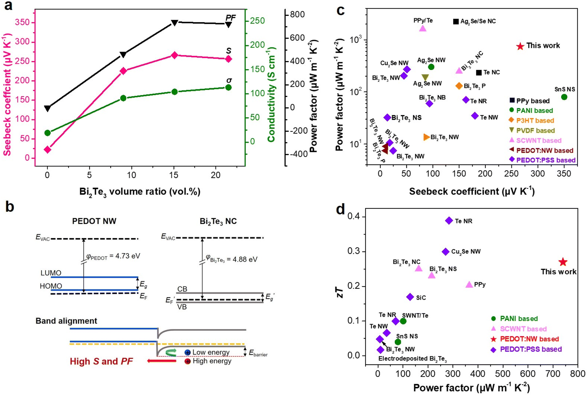 | ||
| Fig. 3 (a) Seebeck coefficient, electrical conductivity, and power factor of p-type Bi2Te3@PEDOT NW films as a function of Bi2Te3 volume ratio. (b) Band structures of the PEDOT NW and Bi2Te3 nanocrystal with the band alignment at the interface. The energy barrier (Ebarrier) scatters low-energy holes (blue ball) and selectively passes high-energy holes (red ball). Comparison of the (c) power factor and (d) zT at 300 K in this work with the data of organic/inorganic composite TE materials reported in the literature. | ||
The σ increases almost linearly from the pure PEDOT NW (19.1 S cm−1) to the 21.5 vol%-Bi2Te3@PEDOT NW film (104.3 S cm−1), showing a σ enhancement of ∼5.5 times. This elevation in σ could be explained based on the following aspects. As analyzed with XRD patterns, the Bi2Te3 nanocrystal layer with high σ becomes gradually continuous and dense, playing an important role in facilitating the electrical transport in the Bi2Te3@PEDOT NW film as Bi2Te3 content increases. The high Bi2Te3 content in the 21.5 vol%-Bi2Te3@PEDOT NW film contributes to higher carrier concentration than that of the 15 vol%-Bi2Te3@PEDOT NW film. Hence the electrical conductivity of the Bi2Te3@PEDOT NW film continuously increases with increasing Bi2Te3 content, which is different from the variation of the Seebeck coefficient.
The power factor (PF = S2σ) of Bi2Te3@PEDOT NW films embodies the synergistic effect of S and σ, reaching a peak PF value of 740.2 μW m−1 K−2 in the 15 vol%-Bi2Te3@PEDOT NW film, which is ∼32 times higher than that of the pristine PEDOT NW film.47 Moreover, Seebeck coefficients and power factors of organic/inorganic TE composites in reported literature are summarized in Table S4† and Fig. 3c, illustrating that the TE properties of the 15 vol%-Bi2Te3@PEDOT NW film in our work stands among a competitive level.
Regarding the figure of merit zT, the in-plane thermal conductivity (k) of the 15 vol%-Bi2Te3@PEDOT NW film was measured to be ∼0.82 W m−1 K−1 at 300 K by the self-heating 3ω method.48,49 At 300 K, the k of the PEDOT NW scaffold was measured to be 0.98 W m−1 K−1, while the k of thermal-shocked Bi2Te3 was measured to be 0.62 W m−1 K−1,44 which is much lower than that of a typical Bi2Te3 crystal (1.35–1.65 W m−1 K−1)50,51 due to numerous internal pores filled with low heat-conducting air. According to the principle of thermal resistance in parallel, the k value of the Bi2Te3@PEDOT NW film at 300 K would be lower than that of both components. On the other hand, numerous nanoscale boundaries generated between Bi2Te3 nanocrystals and PEDOT NWs serve as phonon scattering centers and thus further reduce the total κ for the Bi2Te3@PEDOT NW composite. Thus, the measured k of 0.82 W m−1 K−1 is reliable. The zT value of the 15 vol%-Bi2Te3@PEDOT NW film can be calculated to be ∼0.27, as shown in Fig. 3d, also standing in a competitive level among organic/inorganic composite TE materials reported in the literature.
2.3 Mechanical flexibility of p-type Bi2Te3@PEDOT NW films
Besides the TE properties, the flexibility of composite TE films is also crucial for practical wearable applications, which enables TE electronics to maintain stable output performance under mechanical deformation.52,53 For mechanical flexibility assessment, the 15 vol%-Bi2Te3@PEDOT NW film in our work was tested by bending along glass tubes with different radii. The resistances (R) of the bent Bi2Te3@PEDOT NW films were measured and normalized using the original resistance (R0) as a reference. The relative resistance variation of the 15 vol%-Bi2Te3@PEDOT NW film at different bending radii is shown in Fig. 4a. R/R0 slightly increases with decreasing bending radius (r) from 25 mm to 7.5 mm. As the bending radius dramatically decreases to 3 mm, R/R0 dramatically goes up, which can be attributed to the breakage of the relatively rigid Bi2Te3 nanocrystal layer (Fig. S8†). However, R increases by only 4% at a bending radius of 7.5 mm compared to R0, indicating good flexibility of the 15 vol%-Bi2Te3@PEDOT NW film. In addition, the cyclic bending test was also conducted as shown in Fig. 4b. At a bending radius of 7.5 mm, the 15 vol%-Bi2Te3@PEDOT NW film retains almost the same original resistance value in the first 100 cycles but the value increases vigorously after that. But the resistance is maintained well even after 200 bending cycles when the bending radius increases up to 15 mm. | ||
| Fig. 4 Resistance changes of the 15 vol%-Bi2Te3@PEDOT NW film as a function of (a) bending radius and (b) bending cycle at bending radii of 7.5 mm and 15 mm. Insets show the diagram of the bending test and the photograph of the bent 15 vol%-Bi2Te3@PEDOT NW film. Comparison of the resistance change in the 15 vol%-Bi2Te3@PEDOT NW film with that in composite films in the literature as a function of (c) bending radius and (d) bending cycle. ΔR/R0 was set within 5%. | ||
A PEDOOT NW scaffold consisting of highly ordered PEDOT NWs has abundant nanovoids, which provides large specific surface area for Bi2Te3 deposition. An interlocked Bi2Te3/PEDOOT NW interfacial contact can be formed, contributing to good structural maintenance during dramatical deformation and repetitive bending cycles. As shown in Fig. 4c and d, the mechanical stability of the 15 vol%-Bi2Te3@PEDOT NW free-standing film in this work is at a high level,54–66 especially compared with the composite TE films on flexible conductive supporting substrates.57,60,62,63
2.4 Thermoelectric power generation performance of the cross-plane power generator
Based on TE performance of Bi2Te3@PEDOT NW films, we fabricated a cross-plane TE power generator (TEG) as shown in Scheme S3.† Both p-type and n-type 15 vol%-Bi2Te3@PEDOT NW films were selected as TE leg materials. The Seebeck coefficient and electrical conductivity of the n-type 15 vol%-Bi2Te3@PEDOT NW film were measured to be −158.1 μV K−1 and 112 S cm−1, respectively (Fig. S9†). Fig. 5a shows the diagram of the cross-plane TEG (lateral size of 14 mm × 6 mm and thickness of 5 mm), in which 16 TE legs (8 p–n pairs) were embedded in porous PDMS, electrically connected with Ga75In25, and encapsulated with a PDMS cover. | ||
| Fig. 5 (a) Schematic illustration of the electrical series connection of 16 TE legs and operating mechanism when the top side is exposed to a heat source. (b) Output power density as a function of external resistance at different applied temperature differences. (c) Output voltage density and output power density as a function of circuit current at different applied temperature differences. (d) Comparison of the normalized output power density (specific power) of the cross-plane TEG in our work with the data reported in the literature including that of organic based, organic/inorganic based, and inorganic based TEGs integrated in textile or non-textile substrates. | ||
As a given temperature difference (ΔT) is applied along the out-of-plane direction of the cross-plane TEG, the open-circuit voltage (Voc) is linear to the applied ΔT as demonstrated in Fig. S11a.†Voc values can be theoretically estimated from the equation Voc = (|Sp| + |Sn|) × ΔT × N, where N is the number of p–n pairs. The measured Voc can reach 54.7 mV at a ΔT of 17.8 K, which is close to the theoretically calculated value (60.5 mV at a ΔT of 17.8 K) (Explanatory note 1 and Table S5†). Fig. 5b and c show the output power density and output voltage density of the cross-plane TEG at different ΔT values, respectively. The maximum output power density Pmax occurs as the internal resistance (r) is equal to the external resistance (R).44,67 The Pmax achieves a peak value of 3.48 μW cm−2 at a ΔT of 17.8 K as R = 250 Ω. As shown in Fig. 5c, the output voltage also increases as the applied ΔT increases, showing a voltage density up to 65.1 mV cm−2 at ΔT = 17.8 K. The circuit current is negatively linear to the output voltage, achieving a circuit current of 208.8 μA at ΔT = 17.8 K. A higher output voltage and power can be further realized by operating the cross-plane TEG at larger ΔT and preparing large-area cross-plane TEGs with more pairs of p-type and n-type TE legs (Explanatory note 2 and Table S6†). Provided that a ΔT of 80 K is applied, a corresponding Pmax of 70.6 μW cm−2 can be obtained (Fig. S11b†).
As shown in Fig. 5d, we normalized the reported output powers of various cross-plane TEGs39,67–76 by dividing the area and the applied ΔT in unit of nW cm−2 K−2. Our cross-plane TEG shows a specific power of 10.7 nW cm−2 K−2, which is much higher than that of most organic and organic/inorganic based TEGs, and even some inorganic based TEGs. The higher power output performance is believed to originate from careful optimization of the TE properties of Bi2Te3@PEDOT NW films and the proper design of TEG. Moreover, we also calculated the density of TE legs in these cross-plane TEGs. The density of TE legs of our cross-plane TEG is up to 19 pieces per cm2, which is just inferior to that of the doped-CNTY based TEG75 and stands in a highly competitive level.
2.5 Thermoelectric-powered temperature sensor array
Due to the ultrahigh Seebeck coefficient, we also investigated the temperature sensing performance of the p-type 15 vol%-Bi2Te3@PEDOT NW film based sensor. As shown in Fig. S12a,† each TE leg, which is electrically connected with external copper electrodes and encapsulated with a PDMS cover, can act as an independent TE-powered temperature sensor. The thermovoltage (Vtherm) can be used to assess the temperature-sensing response. Fig. S12b† presents the real-time Vtherm of the sensor at different temperature differences within 1 K. Notably, even a small ΔT of 0.05 K is clearly detected with a Vtherm of 13 μV. Fig. S12c and d† show the good stability of the sensor at different large temperature differences, with respect to the heating time and heating–cooling cycles. The stable and reproducible thermoelectric conversion enables sensitive detection of the TE-powered temperature sensor.According to the aforementioned temperature sensing performance of one TE leg, a flexible cross-plane temperature sensor array consisting of 16 TE legs (16 sensing units) was fabricated. Fig. 6a shows the schematic diagram of the cross-plane temperature sensor array. The ends of all TE legs on the measured side were separately connected using conducting Ga75In25 with external copper electrodes (a1–a16). As for the other ends of all TE legs on the reference side, they were all covered and connected by one thin Ga75In25 layer instead of being separately connected with 16 individual Ga75In25 conducting leads, which was further connected with an external copper electrode (b). This design is different from others in the literature, resulting in significantly reduced numbers of involved electrodes. Vtherm between an (n = 1, 2, 3…16) and b can be captured one by one when a ΔT is applied along the out-of-plane direction of the cross-plane temperature sensor array. As shown in Fig. 6b, the sensor array shows excellent flexibility. It can be bent and twisted, indicating its good conformability with curved surfaces, e.g. human skin.
 | ||
| Fig. 6 (a) Schematic diagram and (b) optical photographs showing mechanical flexibility, including bending and twisting deformation of the cross-plane temperature sensor array. (c and d) Demonstration of the temperature-sensing performance on curved surfaces by attaching the sensor array to bottles with different radii containing hot and cold water. | ||
As stated in Explanatory note 3,† the temperature detected by each sensing unit can be calculated using Tm = 3.846Vthem + T0 + 0.533, where T0 is the temperature of the reference side, e.g. room temperature, and Tm is the temperature of the detected point. Hence the temperature mapping was diagramed. First, we characterized the hot point detection of the cross-plane sensor array by covering different sensing units with a human finger. The corresponding temperature mappings are shown in Fig. S13,† which clearly demonstrate the temperature distributions, thus realizing the temperature detection and location. Moreover, practical temperature detection and location on curved surfaces is demonstrated. Fig. S14† shows the conformance and flexibility of the cross-plane sensor array. It can even be closely attached to a tube with a small radius of 4 mm. Then the cross-plane sensor array was attached to vials with different radii containing hot and cold water, where the ambient temperature is a T0 of 21.8 °C. Fig. 6c shows the temperatures detected by 8 sensing units when the lower half of the sensor array is attached to a vial (radius of 20 mm) containing hot water (50 °C). Likewise, as shown in Fig. 6d, the temperatures of 8 cold points can be observed when the lower half of the sensor array is attached to a vial (radius of 10 mm) containing cold water (4 °C), indicating accurate temperature response and great potential in wearable temperature monitoring applications of the sensor array.
3 Conclusion
Herein a sandwich-like Bi2Te3 nanocrystal/PEDOT nanowire composite film is constructed through a facile thermal deposition process with further thermal-shock treatment. Taking advantage of high thermoelectric properties of inorganic alloy and the flexible polymer nanowire scaffold, the organic/inorganic composite film exhibits a comparatively high thermoelectric performance and mechanical flexibility, in which the optimal power factor is 740.2 μW m−1 K−2 (corresponding zT of 0.27) with an optimal Seebeck coefficient of 266.4 μV K−1 at room temperature. Cross-plane thermoelectric devices based on the aforementioned composite film exhibit good performances of thermoelectric power generation and temperature sensing. Utilizing the out-of-plane temperature difference, the cross-plane thermoelectric generator shows a maximum power density of 3.48 μW cm−2 at a temperature difference of 17.8 K outperforming most organic and organic/inorganic based cross-plane TEGs, while the conformal thermoelectric-powered temperature sensor array exhibits high and stable thermal sensitivity with a resolution of 0.05 K, laying the foundation for wearable power generation and temperature monitoring applications.4 Experimental
4.1 Chemicals and materials
PEDOT nanowires (PEDOT NWs) were synthesized in our lab. P-type and n-type bismuth telluride (Bi2Te3, 99.99%) powder were provided by Changsha Santech Materials Co., Ltd (China). Poly(dimethylsiloxane) (PDMS) and the curing agent (Sylgard™ 184) were purchased from Dow Corning Corporation. N-Hexane was bought from Sinopharm Chemical Reagent Co., Ltd (China). Liquid metal (Ga75In25 with a resistivity of 29.4 μΩ cm and thermal conductivity of 26.43 W m−1 K−1) was purchased from Dongguan Dingguan Metal Technology Co., Ltd (China). Polylactic acid (PLA) tubes. All chemicals were of analytical grade and used as received.4.2 Preparation of Bi2Te3@PEDOT NW sandwich-like films
Flexible Bi2Te3@PEDOT NW sandwich-like films were prepared as follows. Free-standing PEDOT NW scaffolds were prepared as previously reported.77,78 P- and n-type Bi2Te3 powder were respectively evenly and compactly deposited in/onto PEDOT NW scaffolds through the high-vacuum thermal evaporation process (Fig. 1a). That is, Bi2Te3 powder was molten to sublimate, and gaseous Bi2Te3 was transported from the evaporation source and re-nucleated on the surface of PEDOT NWs, forming tight interaction. The two surfaces of PEDOT NW scaffolds were equally deposited with Bi2Te3. Thus, Bi2Te3@PEDOT NW sandwich-like films were obtained. Diverse contents of Bi2Te3 on PEDOT NW scaffolds were controlled by varying the evaporation time. The thickness of the thermally deposited Bi2Te3 layer can be recorded using a FTM-V film thickness monitor.To obtain an alloyed Bi2Te3 nanocrystal for better electrical conductivity, a thermal-shock treatment using intense current was applied. Bi2Te3@PEDOT NW films were heated between two pieces of carbon paper (Toray, TGP-H-060, 62 mm in length, 12 mm in width and 0.19 mm in thickness) at a current of 3.5 A for 10 s under an Ar atmosphere (supply power was ∼37 W) in a glovebox (<1 ppm H2O and <1 ppm O2). As shown in Fig. S2,† the temperature of the carbon paper surface is ∼220 °C.
4.3 Characterization of Bi2Te3@PEDOT NW films
Surface and cross-sectional morphologies of Bi2Te3@PEDOT NW films were observed by using a field-emission scanning electron microscope (FESEM, Hitachi SU8010) with energy dispersive spectroscopy (EDS) elemental mapping analysis. The crystallographic structure of Bi2Te3@PEDOT NW films was examined by using an X-ray diffractometer (XRD, Bruker D8 Advance) using Cu Kα (λ = 1.5406 Å) radiation at 40 kV and 200 mA.4.4 Thermoelectric property measurements of Bi2Te3@PEDOT NW films
The room-temperature thermoelectric properties of Bi2Te3@PEDOT NW films, including the Seebeck coefficient, electrical conductivity, and thermal conductivity, were measured by employing a self-built test system according to our previous work.47,77 The Seebeck coefficient was calculated by using the formula S ∼ −ΔV/ΔT. The thermovoltage ΔV was recorded by using a Keithley 2182A and the temperature difference ΔT was calculated from the measured temperature data by using a Fotric 226 thermal infrared camera (Scheme S1†). The electrical conductivity was measured by using two Keithley 2400 current source meters using a standard van der Pauw (VDP) method (Scheme S2a†). Thicknesses of all samples were precisely determined from cross-sectional FESEM images, and at least five different locations were measured for each sample. The in-plane thermal conductivity was measured by the self-heating 3ω method (Scheme S2b and c†).48,49 The variable-temperature thermal conductivity test system consists of an dewar (East Changing Technology Co. Ltd) with liquid nitrogen as the coolant and a TC-202 temperature controller.4.5 Fabrication of the cross-plane thermoelectric generator
Porous PDMS (Fig. S10†) was adopted as supporting substrate in the cross-plane thermoelectric generator (TEG). P- and n-type 15 vol%-Bi2Te3@PEDOT NW films were cut into strips (2 mm × 23.5 μm × 5 mm). After thermal-shock treatment, as shown in Scheme S3,† p- and n-type TE legs were alternately fixed between two PDMS layers using a thin layer of semi-solid PDMS as the binder. The thickness of each PDMS layer and the space between two TE legs are 2 mm. The final cross-plane TEG with a thickness of 5 mm was obtained consisting of 16 TE legs (8 p–n pairs), which are electrically connected in series using liquid metal (Ga75In25) instead of conventional metal wires. For the sake of wearable safety and stability, Ga75In25 conducting wires were encapsulated with a transparent PDMS cover.4.6 Thermoelectric power generation performance of the cross-plane TEG
A temperature difference is generated by placing the cross-plane TEG on a polyimide heating film (PI heater) with the other side exposed to air. The output voltage was recorded by using a Keithley 2182A. The output power was calculated by using the formula , where U is the open-circuit voltage, r is the internal resistance of the cross-plane TEG, and R is the external resistance which is altered with a variable resistor. The equivalent circuit of the cross-plane TEG supplying power is depicted in Scheme S4,† where Voutput and I are the voltage on the external resistance and the circuit current.
4.7 Fabrication of the cross-plane temperature sensor array
For convenience and high conversion performance, only the p-type 15 vol%-Bi2Te3@PEDOT NW film was used in the cross-plane temperature sensor array. Similar to the aforementioned cross-plane TEG, p-type TE legs were embedded into a flexible porous PDMS supporting substrate. As for electrical connection, it is worth mentioning that all ends of TE legs on the same side of the device were integrated by a thin Ga75In25 layer, which was connected with an external copper electrode and ensures uniform temperature distribution of the reference side during the temperature monitoring. Likewise, conducting Ga75In25 wires were separately painted connecting the other ends of TE legs with copper external electrodes. Ga75In25 was also encapsulated with a transparent PDMS cover.4.8 Practical application demonstration of the cross-plane temperature sensor array
To demonstrate temperature monitoring performance of the cross-plane temperature sensor array, the side covered with the whole Ga75In25 layer of the cross-plane temperature sensor array was placed in air, and the other side was attached to the surfaces of objects to be measured or monitored. When a certain ΔT is applied between the top and bottom ends of the cross-plane temperature sensor array, the thermovoltage (Vthem) of each TE leg can be measured.Data availability
The data supporting our findings in this work are available from the corresponding author K. Z. upon reasonable request.Author contributions
K. Zhang conceived the idea and supervised the project. M. Du designed the experiments, prepared all PEDOT NW-based samples, conducted all characterization studies, measurements and data analysis, and drew all figures. K. Zhang and M. Du prepared the initial manuscript. All the authors discussed the results and contributed to reviewing the manuscript.Conflicts of interest
There are no conflicts to declare.Acknowledgements
The authors are thankful for financial supports from the National Natural Science Foundation of China (51973034) and the Fundamental Research Funds for the Central Universities (2232022G01 and 19D110106).References
- Z. Fan, P. Li, D. Du and J. Ouyang, Adv. Energy Mater., 2017, 7, 1602116 CrossRef.
- Z. Fan, D. Du, H. Yao and J. Ouyang, ACS Appl. Mater. Interfaces, 2017, 9, 11732–11738 CrossRef CAS PubMed.
- C. L. Hui Shi, Q. Jiang and J. Xu, Adv. Electron. Mater., 2015, 1, 0282 Search PubMed.
- H. Chen, Y. Chen, H. Zhang, W. Cao, C. Fang, Y. Zhou, Z. Xiao, J. Shi, W. Chen, J. Liu and W. Hong, Chin. Chem. Lett., 2022, 33, 523–526 CrossRef CAS.
- O. Bubnova, M. Berggren and X. Crispin, J. Am. Chem. Soc., 2012, 134, 16456–16459 CrossRef CAS PubMed.
- G. H. Kim, L. Shao, K. Zhang and K. P. Pipe, Nat. Mater., 2013, 12, 719–723 CrossRef CAS PubMed.
- Y. Jia, X. Li, F. Jiang, C. Li, T. Wang, Q. Jiang, J. Hou and J. Xu, J. Polym. Sci., Part B: Polym. Phys., 2017, 55, 1738–1744 CrossRef CAS.
- S. Zhang, Z. Fan, X. Wang, Z. Zhang and J. Ouyang, J. Mater. Chem. A, 2018, 6, 7080–7087 RSC.
- O. Bubnova, Z. U. Khan, A. Malti, S. Braun, M. Fahlman, M. Berggren and X. Crispin, Nat. Mater., 2011, 10, 429–433 CrossRef CAS PubMed.
- J. Luo, D. Billep, T. Waechtler, T. Otto, M. Toader, O. Gordan, E. Sheremet, J. Martin, M. Hietschold and D. R. T. Zahn, J. Mater. Chem. A, 2013, 1, 7576–7583 RSC.
- T. A. Yemata, Y. Zheng, A. K. K. Kyaw, X. Wang, J. Song, W. S. Chin and J. Xu, Front. Chem., 2020, 7, 870 CrossRef PubMed.
- S. Zhang, Z. Fan, X. Wang, Z. Zhang and J. Ouyang, J. Mater. Chem. A, 2018, 6, 7080–7087 RSC.
- S. Xu, M. Hong, X. Shi, Y. Wang, L. Ge, Y. Bai, L. Wang, M. Dargusch, J. Zou and Z. Chen, Chem. Mater., 2019, 31, 5238–5244 CrossRef CAS.
- A. K. K. Kyaw, T. A. Yemata, X. Wang, S. L. Lim, W. S. Chin, K. Hippalgaonkar and J. Xu, Macromol. Mater. Eng., 2018, 303, 1700429 CrossRef.
- P. Li, X. Ai, Q. Zhang, S. Gu, L. Wang and W. Jiang, Chin. Chem. Lett., 2021, 32, 811–815 CrossRef CAS.
- J. Xie, J. Wang, Q. Yu, N. A. Khoso and J. Zhao, J. Textil. Res., 2018, 39, 50–55 Search PubMed.
- L. Liang, J. Fan, M. Wang, G. Chen and G. Sun, Compos. Sci. Technol., 2020, 187, 107948 CrossRef CAS.
- L. Liang, X. Wang, M. Wang, Z. Liu, G. Chen and G. Sun, Compos. Commun., 2021, 25, 100701 CrossRef.
- S. Panigrahy and B. Kandasubramanian, Eur. Polym. J., 2020, 132, 109726 CrossRef CAS.
- Y. Lu, Y. Ding, Y. Qiu, K. Cai, Q. Yao, H. Song, L. Tong, J. He and L. Chen, ACS Appl. Mater. Interfaces, 2019, 11, 12819–12829 CrossRef CAS PubMed.
- W. S. Kim, G. Anoop, I. S. Jeong, H. J. Lee, H. B. Kim, S. H. Kim, G. W. Goo, H. Lee, H. J. Lee, C. Kim, J. H. Lee, B. S. Mun, J. W. Park, E. Lee and J. Y. Jo, Nano Energy, 2020, 67, 10427 Search PubMed.
- N. E. Coates, S. K. Yee, B. McCulloch, K. C. See, A. Majumdar, R. A. Segalman and J. J. Urban, Adv. Mater., 2013, 25, 1629–1633 CrossRef CAS PubMed.
- Z. Tian, H. Liu, N. Wang, Y. Liu and X. Zhang, J. Mater. Sci.: Mater. Electron., 2018, 29, 17367–17373 CrossRef CAS.
- J. Xiong, L. Wang, J. Xu, C. Liu, W. Zhou, H. Shi, Q. Jiang and F. Jiang, J. Mater. Sci.: Mater. Electron., 2016, 27, 1769–1776 CrossRef CAS.
- Y. H. K. Eun Jin Bae, K.-S. Jang, C. Lee, S. Y. Cho, E. J. Bae, Y. H. Kang, K. S. Jang, C. Lee and S. Y. Cho, Nanoscale, 2016, 8, 10885–10890 RSC.
- W. Thongkham, C. Lertsatitthanakorn, K. Jiramitmongkon, K. Tantisantisom, T. Boonkoom, M. Jitpukdee, K. Sinthiptharakoon, A. Klamchuen, M. Liangruksa and P. Khanchaitit, ACS Appl. Mater. Interfaces, 2019, 11, 6624–6633 CrossRef CAS PubMed.
- B. Zhang, J. Sun, H. E. Katz, F. Fang and R. L. Opila, ACS Appl. Mater. Interfaces, 2010, 2, 3170–3178 CrossRef CAS PubMed.
- Q. Jiang, C. Liu, H. Song, J. Xu and Z. Zhu, Int. J. Electrochem. Sci., 2014, 9, 7540–7551 Search PubMed.
- Y. Du, K. F. Cai, S. Chen, P. Cizek and T. Lin, ACS Appl. Mater. Interfaces, 2014, 6, 5735–5743 CrossRef CAS PubMed.
- A. Rahman, A. Umar and H. Othman, Phys. E Low-dimens. Syst. Nanostruct., 2015, 66, 293–298 CrossRef CAS.
- Y. Lu, Y. Qiu, K. Cai, X. Li, M. Gao, C. Jiang and J. He, Mater. Today Phys., 2020, 14, 100223 CrossRef.
- L. Huang, J. Chen, Z. Yu and D. Tang, Anal. Chem., 2020, 5, 2545–2554 Search PubMed.
- C. J. An, Y. H. Kang, H. Song, Y. Jeong and Y. C. Song, ACS Appl. Energy Mater., 2018, 2, 1093–1101 CrossRef.
- F. Zhang, Y. Zang, D. Huang, C. Di and D. Zhu, Nat. Commun., 2015, 6, 8356 CrossRef CAS PubMed.
- C. K. Jeong, K. I. Park, J. H. Son, G. T. Hwang, S. H. Lee, D. Y. Park, H. E. Lee, H. K. Lee, M. Byun and K. J. Lee, Energy Environ. Sci., 2014, 7, 4035–4043 RSC.
- L. E. Bell, Science, 2008, 321, 1457–1461 CrossRef CAS PubMed.
- K. Chatterjee and T. K. Ghosh, Molecules, 2021, 26, 3154 CrossRef CAS PubMed.
- M. Massetti, F. Jiao, A. J. Ferguson, D. Zhao, K. Wijeratne, A. Würger, J. L. Blackburn, X. Crispin and S. Fabiano, Chem. Rev., 2021, 121, 12465–12547 CrossRef CAS PubMed.
- C. Zheng, L. Xiang, W. Jin, H. Shen, W. Zhao, F. Zhang, C. Di and D. Zhu, Adv. Mater. Technol., 2019, 4, 1900247 CrossRef CAS.
- B. Poudel, Q. Hao, Y. Ma, A. Minnich, B. Yu, X. Yan, D. Wang, A. Muto, D. Vashaee, X. Chen, J. Liu, M. S. Dresselhaus, G. Chen and Z. Ren, Science, 2008, 320, 634–638 CrossRef CAS PubMed.
- S. Jimenez, J. G. Perez, T. M. Tritt, S. Zhu, J. L. Sosa-Sanchez, J. Martinez-Juarez and O. López, Energy Convers. Manag., 2014, 87, 868–873 CrossRef CAS.
- P. Y. Lee, J. Hao, T. Y. Chao, J. Y. Huang, H. L. Hsieh and H. C. Hsu, J. Electron. Mater., 2014, 43, 1718–1725 CrossRef CAS.
- X. Lu, Q. Zheng, S. Gu, R. Guo, L. Su, J. Wang, Z. Zhou, Y. Fan, W. Jiang and L. Wang, Chin. Chem. Lett., 2020, 31, 880–884 CrossRef CAS.
- Y. Zheng, X. Han, J. Yang, Y. Jing, X. Chen, Q. Li, T. Zhang, G. Li, H. Zhu and H. Zhao, Energy Environ. Sci., 2022, 15, 2374–2385 RSC.
- O. Bubnova and X. Crispin, Energy Environ. Sci., 2012, 5, 9345–9362 RSC.
- G. Kim and K. P. Pipe, Phys. Rev. B, 2016, 86, 6709–6717 Search PubMed.
- J. Zhang, K. Zhang, F. Xu, S. Wang and Y. Qiu, Compos. B Eng., 2018, 136, 234–240 CrossRef CAS.
- Z. L. Wang, D. W. Tang and W. G. Zhang, J. Phys. D: Appl. Phys., 2007, 15, 4686–4690 CrossRef.
- Y. Sun, L. Qiu, L. Tang, H. Geng, H. Wang, F. Zhang, D. Huang, W. Xu, P. Yue and Y. S. Guan, Adv. Mater., 2016, 28, 3351–3358 CrossRef CAS PubMed.
- D. Park, S. Park, K. Jeong, H. S. Jeong, J. Y. Song and M. Cho, Sci. Rep., 2016, 6, 19132 CrossRef CAS PubMed.
- Q. He, W. Zhang, X. Liu and H. Song, Mod. Phys. Lett. B, 2022, 36, 28–29 Search PubMed.
- B. Russ, A. Glaudell, J. J. Urban, M. L. Chabinyc and R. A. Segalman, Nat. Rev. Mater., 2016, 1, 1–14 Search PubMed.
- C. Zheng, L. Xiang, W. Jin, H. Shen, W. Zhao, F. Zhang, C. a. Di and D. Zhu, Adv. Mater. Technol., 2019, 4, 1900247 CrossRef CAS.
- H. W. Ju, J. K. Sun and B. J. Cho, Energy, 2014, 73, 506–512 CrossRef.
- C. Ou, A. L. Sangle, A. Datta, Q. Jing, T. Busolo, T. Chalklen, V. Narayan and S. K. Narayan, ACS Appl. Mater. Interfaces, 2018, 19580–19587 CrossRef CAS PubMed.
- L. Wang, Z. Zhang, L. Geng, T. Yuan, Y. Liu, J. Guo, L. Fang, J. Qiu and S. Wang, Energy Environ. Sci., 2018, 11, 1307–1317 RSC.
- B. Wu, Y. Guo, C. Hou, Q. Zhang, Y. Li and H. Wang, Adv. Funct. Mater., 2019, 29, 1900304 CrossRef.
- Y. Ding, Y. Qiu, K. Cai, Q. Yao, S. Chen, L. Chen and J. He, Nat. Commun., 2019, 10, 841 CrossRef PubMed.
- D. Kong, W. Zhu, Z. Guo and Y. Deng, Energy, 2019, 175, 292–299 CrossRef CAS.
- K. Buks, J. Andzane, L. Bugovecka, M. V. Katkov, K. Smits, O. Starkova, J. Katkevics, A. Bērziņš, L. Brauna and V. Voikiva, Adv. Mater. Interfac., 2022, 9, 2200318 CrossRef CAS.
- J. Shi, X. Wu, X. Geng, L. Hu, F. Liu, W. Ao and C. Zhang, Chem. Eng. J., 2023, 458, 141450 CrossRef CAS.
- X. Chen, L. Feng, P. Yu, C. Liu, J. Lan, Y. Lin and X. Yang, ACS Appl. Mater. Interfaces, 2021, 13, 5451–5459 CrossRef CAS PubMed.
- C. Liu, D. L. Shan, Z. H. Shen, G. K. Ren and C. W. Nan, Nano Energy, 2021, 106380 CrossRef CAS.
- B. Xin, L. Wang, A. L. Febvrier, A. Elsukova, B. Paul, N. Solin and P. Eklund, ACS Omega, 2022, 7, 23988–23994 CrossRef CAS PubMed.
- J. Qin, Y. Du, Q. Meng and Q. Ke, Compos. Commun., 2023, 38, 101467 CrossRef.
- D. Zheng, H. Jin, Y. Liao and P. Ji, Mater. Lett., 2023, 134019 CrossRef CAS.
- X. Yang and K. Zhang, ACS Appl. Mater. Interfaces, 2022, 14, 44704–44712 CrossRef CAS PubMed.
- M. K. Kim, M. S. Kim, S. Lee, C. Kim and Y. J. Kim, Smart Mater. Struct., 2014, 23, 105002 CrossRef.
- J. Choi, Y. Jung, S. J. Yang, J. Y. Oh, J. Oh, K. Jo, J. G. Son, S. E. Moon, C. R. Park and H. Kim, ACS Nano, 2017, 11, 7608–7614 CrossRef CAS PubMed.
- M. Ito, T. Koizumi, H. Kojima, T. Saito and M. Nakamura, J. Mater. Chem. A, 2017, 5, 12068–12072 RSC.
- Y. Shi, Y. Wang, D. Mei, B. Feng and Z. Chen, IEEE Rob. Autom. Lett., 2018, 3, 373–378 Search PubMed.
- T. Lee, K. T. Park, B. C. Ku and H. Kim, Nanoscale, 2019, 11, 16919–16927 RSC.
- N. Wen, Z. Fan, S. Yang, Y. Zhao, T. Cong, S. Xu, H. Zhang, J. Wang, H. Huang and C. Li, Nano Energy, 2020, 78, 105361 CrossRef CAS.
- H. Xu, Y. Guo, B. Wu, C. Hou, Q. Zhang, Y. Li and H. Wang, ACS Appl. Mater. Interfaces, 2020, 12, 33297–33304 CrossRef CAS PubMed.
- Y. Zheng, Q. Zhang, W. Jin, Y. Jing, X. Chen, X. Han, Q. Bao, Y. Liu, X. Wang, S. Wang, Y. Qiu, C. Di and K. Zhang, J. Mater. Chem. A, 2020, 8, 2984–2994 RSC.
- K. T. Park, T. Lee, Y. Ko, Y. S. Cho, C. R. Park and H. Kim, ACS Appl. Mater. Interfaces, 2021, 13, 6257–6264 CrossRef CAS PubMed.
- M. Du, X. Chen and K. Zhang, ACS Appl. Energy Mater., 2021, 4, 4070–4080 CrossRef CAS.
- X. Chen, W. Shi and K. Zhang, ACS Appl. Mater. Interfaces, 2020, 12, 34451–34461 CrossRef CAS PubMed.
Footnote |
| † Electronic supplementary information (ESI) available: Supplementary schemes, figures, explanatory notes, and tables. See DOI: https://doi.org/10.1039/d3ta02876c |
| This journal is © The Royal Society of Chemistry 2023 |