
 Open Access Article
 This Open Access Article is licensed under a Creative Commons Attribution-Non Commercial 3.0 Unported Licence
3D printed inks of two-dimensional semimetallic MoS2/TiS2 nanosheets for conductive-additive-free symmetric supercapacitors†
A.
Panagiotopoulos
 a,
G.
Nagaraju
a,
S.
Tagliaferri
a,
C.
Grotta
a,
P. C.
Sherrell‡
a,
M.
Sokolikova
a,
G.
Cheng
a,
F.
Iacoviello
b,
K.
Sharda
a and
C.
Mattevi
*a
a,
G.
Nagaraju
a,
S.
Tagliaferri
a,
C.
Grotta
a,
P. C.
Sherrell‡
a,
M.
Sokolikova
a,
G.
Cheng
a,
F.
Iacoviello
b,
K.
Sharda
a and
C.
Mattevi
*a
aDepartment of Materials, Imperial College London, Exhibition Road, SW7 2AZ London, UK. E-mail: c.mattevi@imperial.ac.uk
bElectrochemical Innovation Lab, Department of Chemical Engineering, University College London, London WC1E 7JE, UK
First published on 13th July 2023
Abstract
The semimetallic 1T′ and 1T phases of two-dimensional (2D) transition metal dichalcogenides (TMDs) have been attracting considerable attention as promising materials for electrochemical technologies owing to their intrinsic electrical conductivity and exceptionally high ion-intercalation properties. Achieving the 1T′ phase of MoS2 in high concentration and preserving it during device operation are still pressing challenges as the phase is metastable. Herein, we demonstrate 3D printed electrodes of 1T′/1T MoS2/TiS2 nanosheets for microsupercapacitors. The highly concentrated water-based inks of exfoliated 1T′/1T MoS2/TiS2 nanosheets were suitable for the printing of 3D architectures with arbitrary geometry, micron-sized features and spatial uniformity. Such architectures are used as microsupercapacitor electrodes which exhibit an areal capacitance of 448.16 mF cm−2 at a current density of 0.1 mA cm−2. TMD-based microsupercapacitors with high-mass loading (up to 100 mg cm−2) 3D electrodes also exhibited excellent cycling stability and coulombic efficiency over 100![[thin space (1/6-em)]](https://www.rsc.org/images/entities/char_2009.gif) 000 cycles, while retaining the 1T′ phase. Overall, the high mass loading of the printed electrode and the conductivity and the geometry of the electrodes contribute to achieving energy and power density (3.89 μW h cm−2 and 250 μW cm−2, respectively) which are prime amongst those of the TMD-based supercapacitors. This work demonstrates the possibility of formulating and processing inks of 2D TMDs without conductive additives, paving the way towards the manufacturability of electrically conductive device components based on metastable materials.
000 cycles, while retaining the 1T′ phase. Overall, the high mass loading of the printed electrode and the conductivity and the geometry of the electrodes contribute to achieving energy and power density (3.89 μW h cm−2 and 250 μW cm−2, respectively) which are prime amongst those of the TMD-based supercapacitors. This work demonstrates the possibility of formulating and processing inks of 2D TMDs without conductive additives, paving the way towards the manufacturability of electrically conductive device components based on metastable materials.
Introduction
The crystal phases of TMDs with semimetallic character have been attracting increasing interest in the last decade.1 Specifically, the semimetallic 1T′ phase of MoS2 has been extensively studied owing to its electrocatalytic properties for hydrogen evolution,2 electrical conductivity3,4 anisotropic transport and high volumetric capacitance and cyclability.5–7 Thin films of exfoliated MoS2 nanosheets with a predominant 1T′ phase have been reported to exhibit volumetric capacitance in the range of ∼400 to ∼700 F cm−3 in aqueous electrolytes upon intercalation of different ions such as H+, Na+ and K+,6,8,9 as well as organic materials without undergoing major structural modifications. Electron-donating species are likely to be intercalated,10 while a record areal capacitance of 0.63 F cm−2 and a corresponding 436 F cm−3 volumetric capacitance have been recently reported for compact thin films of exfoliated 1T MoS2 nanosheets.8 Areal capacitance is increasingly reported as a figure of merit for the emerging area of miniaturised energy storage devices for portable electronics including on chip systems for the Internet of Things.11 Indeed, an intercalation reaction occurs where charges are transferred from Li (the intercalant) to the conduction band of the host layered compound. The conversion of the 2H phase into the 1T′ phase normally accounts for between ∼60–75% of the at% of the material.12,13 Additionally, such films have demonstrated an ultrahigh rate of operation, owing to the inherent ability of this class of van der Waals materials to intercalate ions between the layers.6,8 Fabricating and testing full devices based on 1T′ MoS2 remains challenging, owing to the metastable nature of this phase. This is not a naturally occurring phase, and it can be obtained via lithium treatment of the 2H phase.2,14 Additionally, the 1T′ phase converts to the 2H phase at temperatures just over 100 °C.13,14 Thus, the thermal treatment of an electrode at higher temperatures would make the electrode semiconducting. The process of lithium intercalation in bulk MoS2 and exfoliation in water, pursued either electrochemically or chemically, normally produces solutions with concentrations in the order of 0.1 mg mL−1.13 TiS2 is another layered material, and it has been a prototypical cathode material for Li-ion batteries15,16 demonstrating capacities and energy densities approaching 250 A h kg−1 and 480 W h kg−1, respectively, and surpassing transition metal oxide cathode materials used for Li-ion batteries. Its fast lithium self-diffusion15,17 is amongst the highest reported, thus favouring fast kinetics. It presents a thermodynamically stable 1T phase which exhibits semimetallic properties and it can easily intercalate Li-ions.18–21 Thus, blending exfoliated MoS2 nanosheets in a predominant 1T′ phase and 1T TiS2 nanosheets would ensure the formation of an electrically conductive network with Li-intercalation properties and with van der Waals forces able to create an interconnected network of flakes. These characteristics would make such a blend promising as a supercapacitor electrode.We have demonstrated the formulation of highly concentrated inks with 50 wt% of 1T′/1T semimetallic MoS2/TiS2 in water which are 3D printable via robocasting, also known as direct ink writing. They have been deposited in a layer-by-layer fashion via robocasting to fabricate symmetric microsupercapacitor electrodes with micron-sized features which can be tested as they are, without the need for thermal treatments. The microsupercapacitor demonstrated a prime areal capacitance of 448.16 mF cm−2 with an energy and power density of 3.89 μW h cm−2 and 250 μW cm−2, respectively. The electrodes exhibit excellent cycling stability and coulombic efficiency over 100000 cycles, while retaining most of the 1T′/1T phase after the electrochemical tests. The additive manufacturability of water based TMD inks paves the way for the development of 3D energy storage devices for use in wearable electronics.
Results and discussion
In this work, we have blended exfoliated 1T′ MoS2 and 1T TiS2 nanosheets to 3D print microsupercapacitors. We have chosen 3D printing in the form of direct ink writing as a manufacturing technique as it offers the possibility to design electrodes with arbitrary geometry and dimensions. Additionally, it is viewed as a sustainable manufacturing technique which could also lead to produce devices at scale. Considering the pseudocapacitive nature of 1T′ MoS2 (ref. 6 and 8) and the high intrinsic conductivity of 1T TiS2,22 we have anticipated that the pseudocapacitive charge storage and the electrochemical adsorption–desorption response at the interface between the electrode and electrolyte will be enabled, which can lead to efficient charge transportation toward high-performance microsupercapacitors. We do not anticipate a clear coulombic contribution from TiS2 due to the nanosized dimension of the platelets.23 The uniqueness of our scalable exfoliation of MoS2/TiS2 nanosheets relies on the non-hazardous and water-based amphiphilic properties of a thermoresponsive co-block polymer (poloxamer). The latter enables the dispersion of the platelets and the achievement of high concentration (>1 mg mL−1) via steric and electrostatic stabilization.24 The resulting formulation is printable via continuous extrusion over three dimensions using a robocasting technique. The poloxamer of choice is Pluronic F127 which consists of a poly(propylene oxide) block between two poly(ethylene oxide) blocks. This is a non-hazardous, biocompatible, and commercially available polymer. The first step of the ink formulation is the lithiation of the bulk powders of MoS2 and TiS2 using LiBH4 at 350 °C for 3 days25 (Scheme 1a, detailed Li-intercalation and exfoliation mechanisms have been included in ESI Page 1†). Upon lithium-ion intercalation, the layered 2H MoS2 bulk powders undergo a partial phase conversion to the 1T′ phase (Scheme 1b). This lithiation process leads to the conversion of more than 50% of 2H MoS2 into 1T′ MoS2, as elucidated by XPS analysis (ESI, Fig. S2†), while upon Li intercalation the TiS2 platelets preserve the 1T phase and show negligible oxidation (Fig. S2g†). The subsequent step is exfoliation into atomically thin nanosheets, which occurs by dispersing the lithiated powders with a water-based poloxamer solution (Scheme 1c). A vigorous reaction of lithium ions with water occurs, liberating H2 which is responsible for the separation of the platelets and the formation of single- and few-layered TMD nanosheets with a lateral size in the micrometre range (Scheme 1d). The highest printable concentration achieved is 50 wt% of MoS2/TiS2. The ink was homogenized without adding any further stabilising agent (Scheme 1e). The thermoresponsiveness of Pluronic enables controlled gelation, which is necessary during the printing process to retain the imparted shape (Scheme 1f). The printability of the inks was investigated via rheological characterisation. As shown in Fig. 1a oscillatory measurements show the ink behaving like a solid material at rest with a storage modulus of 105 Pa. The ink is also able to flow when a stress is applied. Materials concentrations lower than 50 wt%, such as 30 wt%, exhibit a lower storage modulus (ESI, Fig. S1†). The very high mass concentration of our inks provides a viscosity of ∼102–103 Pa s (at a shear rate of 10 s−1), which is much higher than the viscosity normally achieved for inkjet printing, and it is amongst the highest for 3D printing (Fig. 1b). Fig. 1c shows a flow ramp which is indicative of a shear-thinning behaviour. When the shear rate increases, the viscosity drops by orders of magnitude to facilitate extrusion from the syringe. The good rheological properties displayed by the inks allowed the printing of structures with different geometries. Multi-layered, interdigitated, serpentine, and square structures (Fig. 1d) show the stability of unsupported inks without buckling, while woodpile structures show the ability of printing spanning structures. Curved and circular structures of different heights were also demonstrated (Fig. 1d). Computed tomography characterisation (Fig. 1e and f) shows the regularity of the printed serpentine and woodpile structures across layers and the absence of sagging or buckling inside the structures.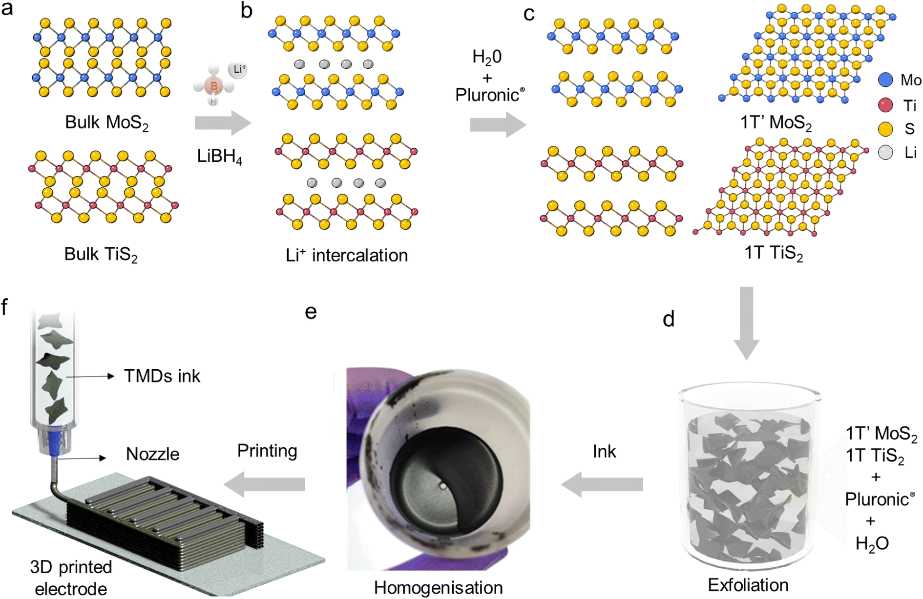 | ||
| Scheme 1 Schematic representation of the synthesis process, exfoliation mechanism and 3D printing of 1T′/1T MoS2/TiS2 inks. (a) Atomic structures of bulk MoS2 and TiS2 and (b) atomic lattices of lithiated MoS2 and TiS2. (c) and (d) Pluronic-water exfoliation process of MoS2 and TiS2. (e) Homogenization of 1T′/1T MoS2/TiS2 inks and (f) extrusion of the corresponding inks through a nozzle. | ||
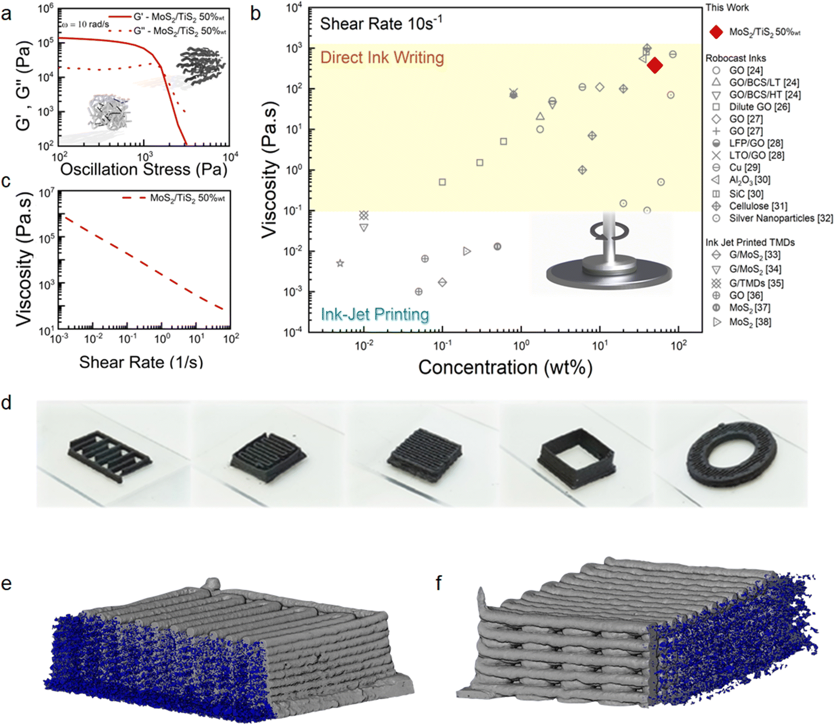 | ||
| Fig. 1 Rheological characteristics of the 1T′/1T MoS2/TiS2 inks and 3D printed structures. (a) Rheological oscillatory measurement of the storage and loss moduli in response to the applied stress for 50 wt% loaded inks at an angular frequency of 10 rad s−1. The inset schematic shows a simplified model for the gel at rest prior to the yield point and gel flowing past the yield point. (b) Comparison of the viscosity versus the active material loading measured at a shear rate of 10 s−1 of various reported values24,26–38 with this work and (c) viscosity flow curve. (d) Photographs of the 3D printed interdigitated electrode, serpentine electrode, woodpile electrode, unsupported high aspect ratio walls, and cylindrical 3D grid structure with a hollow centre. X-ray computed tomographic reconstructions and porosity estimations via image segmentation on 10 × 10 mm 10 layered (e) serpentine and (f) 10 × 10 mm 10 layered woodpile structures. | ||
The regularity of the structures has been also observed via SEM characterisation (Fig. 2a). Cross sectional SEM imaging (Fig. 2b) of the printed struts shows a dense interconnected network of exfoliated flakes of lateral sizes in the range of hundreds of nanometres forming the electrodes. The images were collected after performing a post-printing annealing step to remove the poloxamer to aid the SEM imaging of the microstructure of the struts (Fig. 2c). Bright field TEM imaging shows atomically thin flakes of exfoliated MoS2 and TiS2 with lateral sizes over 1 μm as ink components (Fig. 2d and ESI, Fig. S4 and S5†). A thorough examination of the exfoliated flake edges reveals that single-layered flakes can be achieved (Fig. 2e), and few-layered flakes are often found too. The materials can partially restack, despite the stabilisation by Pluronic. This could be evidenced by the frequently observed moiré patterns,39,40 originating from the angular rotation of restacked single layers (Fig. 2f). Upon lithiation and exfoliation in Pluronic, TiS2 retains the 1T crystal phase of the bulk counterpart as confirmed by the relative intensities of the {100} and {110} diffraction spots in the respective selected area electron diffraction (SAED) patterns (ESI, Fig. S4†), and the flakes display a regular crystalline structure (ESI, Fig. S4†). On the other hand, MoS2 undergoes a 2H to 1T′ crystal phase conversion upon Li intercalation,41 and the 1T′ phase is mostly preserved in the resulting inks (Fig. S2†). The superstructures of two overlapped 2a × a lattices rotated by 120 degrees are often seen in the SAED patterns of few-layered MoS2 flakes (Fig. 2d inset and S5b†). These 2a × a lattices arise from the zigzag distortion in the transition metal plane that is characteristic of the distorted 1T MoS2 crystals (1T′).42,43 The observed superstructures are likely to originate from the “twins” of two individual 1T single crystals, rather than from the intercalated Li residues (Fig. 2d and S5†). It should be noted that although it is likely that trapped Li cations are present in the few-layered exfoliated MoS2 flakes, the observed superstructures in SAED cannot be caused by cation ordering because of the systematic absence of a set of diffraction spots (ESI, Fig. S5†), and thus this proves the presence of the 1T′ crystal phase of MoS2. The conversion of the single layers of MoS2 back into the 2H crystal phase can be caused by the loss of Li cations in agreement with earlier studies,41,44 whereas trapped in the vdW gaps of few-layered flakes, the alkali metal cations preserve the metastable 1T′ phase. The persistency of the 1T′ phase of MoS2 in the printed structures has been attributed to the presence of lithium and lithiated species as detected by secondary ion mass spectrometry (SIMS) characterisation (Fig. 2g–n). The spatial distribution of MoS2 and TiS2 flakes throughout a volume of 40 × 40 × 40 μm (Fig. 2g–n) of the as-printed serpentine structure was directly investigated by time-of-flight secondary ion mass spectrometry (TOF-SIMS). A homogeneous distribution of both types of nanosheets can be detected. Interestingly, the oxidation of the materials is limited to the topmost layer of the 3D printed structures (Fig. 2i, m and ESI Fig. S6†), and MoS2 and TiS2 are equally affected. Importantly, time-of-flight secondary ion mass spectrometry (ToF SIMS) characterisation has (Fig. 2g–l) revealed that a fraction of lithiated MoS2 and TiS2 is found along with the pristine counterparts. The signal of these lithiated LiMoS2 and LiTiS2 species overlaps with that of MoS2 and TiS2 suggesting that the presence of intercalated Li species allows the preservation of the 1T′ phase of MoS2, which is key to achieve good electrical conductivity. A confirmation of this hypothesis is the observed decrease in secondary ion yields after annealing (Fig. 2i and m).
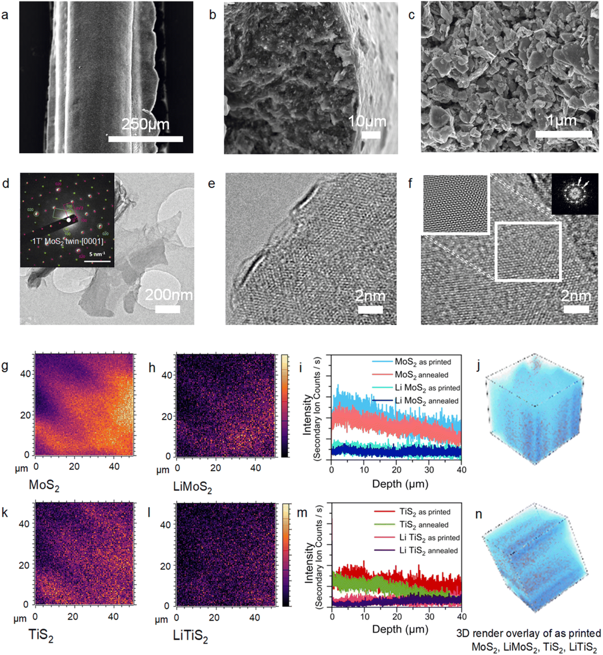 | ||
| Fig. 2 Structural and spectrometric characterisation of the MoS2/TiS2 ink and 3D architectures. (a) Low-magnification SEM image of the as-printed strut (scale bar: 250 μm); (b) cross-sectional SEM image of the extruded MoS2/TiS2 filament (scale bar: 10 μm) (c) SEM image showing the morphology of an annealed MoS2/TiS2 electrode with exposed 2D flakes (scale bar: 1 μm); (d) a representative TEM image of micron-sized exfoliated MoS2 nanosheets; (scale bar: 200 nm) and the corresponding SAED pattern of a few-layered MoS2 flake illustrating the presence of the 1T′ phase (inset, scale bar: 5 nm−1) (e) a high-resolution TEM image of the MoS2 flake edge illustrating the monolayer nature of the exfoliated material; (scale bar: 2 nm) (f) a high-resolution TEM image and a Fourier filtered image (inset) highlighting the Moiré pattern of restacked MoS2 single layers; (scale bar: 2 nm); (g, h, k and l) ToF-SIMS topographic reconstructions of MoS2/TiS2/LiMoS2/LiTiS2 species on the surface of as-printed 3D serpentine structures. (i and m) Depth profiling of MoS2 (blue), Li–MoS2 (turquoise), TiS2 (red) and Li–TiS2 (fuchsia) species present in an as-printed and thermally annealed serpentine structure (j and n) 40 × 40 × 40 μm 3D rendered species overlay topographic reconstruction in an as-printed serpentine structure. MoS2 (blue), Li–MoS2 (turquoise), TiS2 (red) and Li–TiS2 (fuchsia). | ||
Electrochemical performance of 3D MoS2/TiS2 symmetric supercapacitors
To evaluate the electrochemical areal performance of the supercapacitor devices based on 3D patterned MoS2/TiS2 electrodes, we developed symmetric two-electrode prototype cells with a hydrogel electrolyte at room temperature. The 3D electrodes were tested as printed and were entirely made of MoS2/TiS2 (TMDs) suspended in a poloxamer hydrogel, which enables low internal resistance and high electroactive area as discussed below. The hydrogel electrolyte is based on 27% w/v poloxamer and 1 M H2SO4. The thermoresponsive behaviour of the poloxamer is exploited to combine liquid-like electrode wetting and gel-like device stability. 1 M H2SO4/poloxamer electrolyte is conditioned in the liquid phase at 4 °C, poured into a pre-defined shape over the two electrodes and gradually solidifies at room temperature to form a quasi-solid-state supercapacitor device. The ability of the exfoliated MoS2/TiS2 sheets to accommodate a variety of solvated ion intercalants was also examined in a three-electrode system in 1 M aqueous Li2SO4 and ZnSO4 electrolytes (ESI, Fig. S7†). These exhibited capacitive cyclic voltammograms at the scan rates investigated (10000 to 100 mV s−1), suggesting fast and reversible ion adsorption behaviour. MoS2 and TiS2 individual structures were investigated in the 1 M H2SO4/poloxamer electrolyte (Fig. S8†) to assess their individual electrochemical properties. The MoS2 structures exhibit electrocatalytic side-reactions while the TiS2 structures are affected by slow ion intercalation. When MoS2 and TiS2 nanosheets are combined, the electrochemical stability improves without exhibiting electrocatalytic side-reactions. The electrochemical behaviour of MoS2/TiS2 electrodes in terms of rate capability, surface charge resistance and cycling stability, was evaluated using cyclic voltammetry (CV), electrochemical impedance spectroscopy (EIS), galvanostatic charge–discharge (GCD) and chronoamperometric/controlled potential coulometric (CPC) studies. Different electrode configurations (serpentine and woodpile) were compared with thin films to investigate the possible advantage of using 3D structures.
Fig. 3a shows the comparative CV curves of the fabricated microsupercapacitors using the 3D printed structures and thin-film TMDs measured at a constant scan rate of 100 mV s−1. Among the devices measured, the 3D serpentine architectures enable the largest CV integral area, suggesting low resistance and fast charge transport. On increasing the scan rate from 100 to 1000 mV s−1, the CV curves preserve a quasi-rectangular shape, demonstrating a reversible charge storage process without side reactions (ESI, Fig. S9–S11†). Fig. 3b shows the electrochemical cell assembly with 1 M H2SO4/poloxamer hydrogel electrolyte. The electrochemical contribution mechanisms of TMDs were quantified using a power law – and a reformulated power law (Fig. 3c and ESI, Fig. S12–S15†). From such an analysis, the charge storage (Fig. 3c) appears to arise from the combination of electrostatic electrical double-layer capacitance and surface to near-surface pseudocapacitance (slow-kinetics) due to reversible ion adsorption and fast intercalation of solvated ions.45 Upon increasing the scan rate to over 1000 mV s−1 (ESI, Fig. S9–S11†), the CV curves of TMDs demonstrate highly resistive behaviour, which indicates that the accumulated charges are predominantly electrostatic and ion intercalation is possibly not occurring. Monitoring stored charges is instrumental in performance benchmarking but also in comprehending more of the phenomena and mechanisms behind electrochemical energy storage. The electrochemical behaviour and TMD device charge storage are extracted from CV analysis. However, this method is subjective to polarization effects due to the cyclic nature.48 Therefore, a straightforward route which utilises conventional controlled potentiostatic coulometry (CPC) is proposed to examine the electrochemical performance of supercapacitor devices (Fig. 3d–f). Applying a bias voltage over time is a linear way to measure the current.49 The method consists of integrating [ESI, eqn (S1)†] the current at a fixed potential and measuring the flow of charges from one electrode to the other. In this way, it is possible to extract and quantify the charges stored at different potentials across the operating potential spectrum with very high accuracy. Given the nature of the technique, we can monitor the electrochemical contribution mechanisms by gauging the charge slope and the self-discharging time (Fig. 3d and e). Additionally, by normalising the extracted charges from the charging step at 0.5 V, we monitored the capacitance which plateaus at maximum values after 100 s (Fig. 3f). The extracted charges and the normalised capacitance were compared between CV, GCD and CPC techniques (ESI, Fig. S18†). From these observations, it is apparent that CPC could be used as an electroanalytical diagnostic tool to monitor charge storage behaviour and intercalation phenomena among other conventional techniques such as GCD and CV.
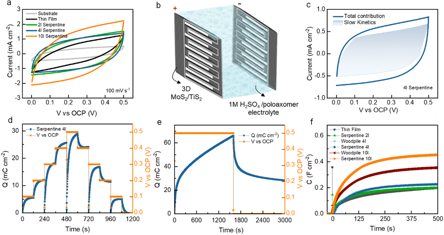 | ||
| Fig. 3 Electrochemical characterisation of printed and thin-film MoS2/TiS2 microsupercapacitors. (a) Cyclic voltammograms of various device components at a scan rate of 100 mV s−1 and (b) schematic representation of the electrochemical cell assembly. (c) Current contribution on a 4 layered serpentine structure obtained at a 100 mV s−1 scan rate. (d) Controlled potential coulometric profiles of stored charges in response to the operating potential window in a 4l serpentine electrode. The electrode was conditioned at 0 V every two potential steps. (e) Controlled potential coulometry at 0.5 V and discharge at 0 V on a 4l serpentine electrode. (f) Capacitance values extracted from controlled potential coulometric profiles of different electrodes at 0.5 V. | ||
The electrochemical capacitance of printed microsupercapacitors was characterized using GCD analysis (Fig. 4a and S16†) by varying the current densities between 1 and 0.1 mA cm−2. The GCD curves across this range showed nearly symmetric triangular plots without an internal voltage drop in woodpile structures, serpentine structures, and thin films. Compared to the thin-film devices, the stacked layers of woodpile and serpentine 3D architectures lead to faster charge storage kinetics and higher areal capacitance, as presented in the capacitance versus current density plots in Fig. 4c. Among the devices measured, the 10 layer serpentine-shaped microsupercapacitor exhibits the highest charge–discharge times, which leads to the highest areal capacitance of 448.16 mF cm−2 at a current density of 0.1 mA cm−2. The displayed rate capability is 30.9% at a high current density of 1 mA cm−2.
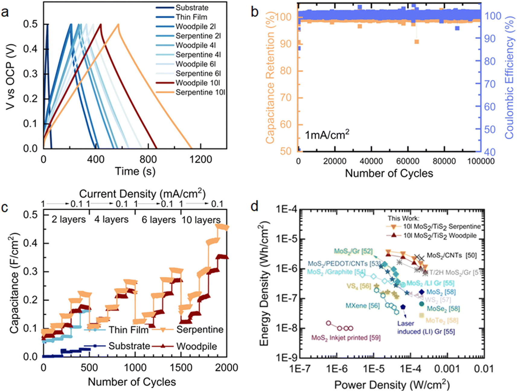 | ||
| Fig. 4 Potentiometric electrochemical characterisation of printed and thin-film MoS2/TiS2 microsupercapacitors. (a) Galvanostatic charge–discharge profiles at a current density of 0.1 mA cm−2 between different electrodes (substrate, thin-film, woodpile, and serpentine architectures). (b) Galvanostatic charge discharge stability test over 100000 cycles at a current density of 1 mA cm−2 on a 4 layered serpentine structure and (c) capacitance values extracted from galvanostatic charge–discharge at different current densities in response to the electrode geometry and added layers. (d) Ragone plot as calculated from extracted values50–59 of CCD in TMD based devices. | ||
The measured capacitance and rate capability of 3D TMDs at increased current densities could be attributed to the large ionic diffusivity as evidenced by the kinetic analyses (Fig. S12–S15†) and high polarizability of covalently bonded S in the TMDs.46 Noticeably, serpentine devices surpass woodpile devices across all current densities and numbers of layers. The high capacitance could be ascribed to the strut stack which enables larger electrolyte ion diffusion paths compared to the woodpile structures and minimizes the resistance. To further investigate the long-term stability of 3D TMDs, rapid charge–discharge measurements were carried out. After 105 cycles at a current density of 1 mA cm−2, the device retained more than 99.1% of its initial capacitance with an excellent coulombic efficiency of 99.8% (Fig. 4b). From electrochemical impedance spectroscopy (Fig. S17†), we conclude that the TMD electrodes are readily ionically accessible throughout the operating potential window, demonstrating low charge transfer resistance.47 Further rate analyses were carried out to evaluate the effect of the number of printing layers and 3D architectures on the electrochemical performance. Areal, gravimetric, and volumetric capacitance variation as a function of the cycle number was reported as shown in Fig. 4c, S20 and S21.† On varying the current densities (from high- to low-current densities), the capacitance also steadily increases for the woodpile and serpentine devices, which suggests that the entire 3D architecture is actively involved in charge storage within their thickness range. This likely originates from the conductivity of the 1T′/1T metallic phase TMDs that initiates rapid charge transportation, as well as from deep electrolyte penetration into the 3D porous electrodes towards high energy storage properties. These metallic properties are also retained in considerable amount after cycling (Fig. S2†). The electrochemical performance of semiconducting 2H phase printed electrodes (after thermal annealing) was measured for comparison. The 1T′/1T metallic phase demonstrated a higher integral current and charge–discharge response compared to the 2H phase electrodes, as presented in Fig. S20.† The Ragone plot presented in Fig. 4d compares the energy storage performance of our 1T′/1T phase 3D electrodes with that of different TMD-based microsupercapacitors reported in the literature. To the best of our knowledge, there were no 3D printed carbon additive-free TMD electrodes, and thus, all comparisons are made with systems where carbon additives were present or TMD based devices that were not 3D printed. Remarkably, the serpentine MoS2/TiS2 microsupercapacitor exhibited a higher energy density of 3.89 μW h cm−2 with a maximum power density of 250 μW cm−2 in poloxamer gel-electrolyte, which are higher than those of the thin-film (1.3 μW h cm−2) and woodpile devices (2.96 μW h cm−2). Moreover, the serpentine 1T′/1T MoS2/TiS2 devices energy and power densities surpass those of most of the previously reported printed TMDs with carbon additive devices (Fig. 4d).50–59 The volumetric and gravimetric performances of all device components are reported in Fig. S21–S23.† Overall, the electrochemical behaviour of exfoliated 1T′/1T MoS2/TiS2 nanosheets is attributed to the reversible surface double layer, near surface ion adsorption and solvated ion intercalation in between the sheets mechanisms.60,61 Additionally, the scalable printing of semimetallic MoS2/TiS2 inks free from conductive carbon additives enables the fabrication of microsupercapacitors with prime energy density and power density with unprecedented cycling stability, opening new opportunities for the development of entirely TMD-based energy storage devices.
Conclusions
In summary, we have demonstrated a one step process of exfoliation and aqueous ink formulation of 1T′/1T MoS2/TiS2 nanosheets in very high concentration (50 wt%). The TMD ink was employed for additive-manufacturing of 3D architectures without the aid of conductive additives. We reveal that different architectures lead to different performances of charge storage, due to different diffusion paths of the electrolyte. Specifically, the serpentine-shaped 3D printed TMDs exhibited a high capacitance of 448.16 mF cm−2 at 90 mg cm−2, and 6.5 F g−1 and 4.5 F cm−3 at 35 mg cm−2 with an exceptionally high cycling stability of 99.1% over 105 charge–discharge cycles. The energy density of 3.89 μW h cm−2 at a power density of 250 μW cm−2 surpasses the present literature values for TMD based supercapacitors. This work paves the way towards the scalable production of semimetallic TMD inks without using any conductive additives for 3D printing of microelectrodes, which can be foreseen to have a broad range of applications, such as in energy storage devices, electrochemical sensors, and water-splitting applications.Experimental section
TMD ink formulation
Molybdenum disulphide and titanium disulphide bulk powders were mixed in a 50:50 molar ratio (MoS2:TiS2) and then combined with lithium borohydride in a glovebox inert environment, with a molar ratio of 1:2.5 (total TMDs:LiBH4). The mixed powders were gradually heated and held at 350 °C for 72 h before cooling down. Heating and cooling were carried out for a span of 12 h, respectively. Pluronic-F127 powders were dispersed in de-ionized water with a volume of 25% w/v, which was found to be optimal for the carrier hydrogel, and conditioned at 4 °C. Intercalated powders were transferred in a PTFE fire-proof container, directly exfoliated with one third of the carrier hydrogel volume and quenched with the two others, while stirring continuously to result in 30 wt% and 50 wt% inks of the combined active material versus the carrier hydrogel. The subsequent formulation was then homogenised using a commercial planetary mixer conditioned at 2000 rpm for 2 min and defoamed at 2200 rpm for another 2 min, to reorient the exfoliated nanosheets, saturate hydrolysis, remove air bubbles and ensure optimum dispensing flow during additive manufacturing. TMD ink formulations were then stored at 4 °C. All reagents were purchased from Merck Sigma-Aldrich and were used as received. A commercial conditioning planetary mixer model was purchased from Intertronics, model Thinky ARE-250.
Rheological characterisation
Rheological properties of the TMD inks were investigated using a rotational mapping geometry of 40 mm parallel Peltier Plate steel loaded on a rotational Discovery Hybrid rheometer HR1 provided by TA Instruments, after friction and temperature calibration at a fixed gap of 1000 μm, 25 °C temperature and using a solvent trap to minimise water loss. Oscillatory tests were performed at 10 rad s−1 and flow measurements, at a shear rate from 10−3 to 102 s−1. Each measurement was performed three times with a cleaning and recalibrating stage in between.Preparation of thin film electrodes
Graphite foil sheets were masked at 1 × 10 cm dimensions with 1 layer of 3 M Scotch Magic tape adhesive tape type 810 with 62.5 μm thickness. TMD inks were then spread by using a doctor-blade to control the thickness of thin films at 40 μm post-drying, and then cut into 1 × 1 cm of active material.3D printing of TMD inks
TMD inks were loaded into 3 mL polypropylene syringes with metal tipped blunt nozzles with inner diameters of 200 and 410 μm. The syringes were mounted onto the three-axis stage of a custom 3D printer loaded on a gantry crane and subsequently dispensed in different 3D shapes on a variety of flat substrates by using a brushless ball screw and syringe displacement actuators, which provided a feed rate of 6 mm s−1. The 3D shapes were computed aided designs as .stl files and translated into G-code using the manufacturer’s proprietary software. Syringes and nozzles were purchased from Nordson EFD precision dispensing systems and the bespoke 3D printer system was from 3D Inks LLC.Thermal annealing
As-printed architectures were thermally annealed for obtaining the 2H phase in a vacuum tube furnace under an argon flux for 3 h at 470 °C with a 25 °C min−1 heating rate.Materials characterisation
000 mV s−1 and vice versa. Five cycles were performed at each scan rate, of which the third was visualised. Impedance spectroscopy was performed in a frequency range ramping from 0.02–100000 Hz and 100000–0.02 Hz with a fixed potential across the whole device operating potential spectrum from 0.0 V–0.5 V–0.0 V, with a 0.1 V step size. Galvanostatic charge–discharge measurements were performed at a fixed current in the 0.1–1 mA range over 100 and 1000 cycles for each current density and over 100000 for 1 mA (each charge/discharge cycle occurred in 40 s which translates into 41 days of continuous cycling). The 50th cycle was visualised each time. Chronoamperometric/controlled potential coulometric studies were performed across the device operating potential window (0.0 V–0.5 V–0.0 V) with a 0.1 V step size. Prior to any measurement, each cell was conditioned at 0.0 V for at least 120 s. Furthermore, impedance spectroscopy was performed after each set of characterisation studies to gauge the ageing profile. All measurements were carried out using a series of Gamry 1010E interface bipotentiostats/galvanostats.
Author contributions
C. M. conceived and designed the work. A. P., S. T., and C. G. performed the TMD exfoliation, the ink formulation, and the 3D printing. A. P., G. N., S. T., and P. S. performed the device fabrication and the electrochemical characterization. M. S. performed TEM characterization. G. C. performed XPS characterization. F. I. performed X-ray computed tomography. C. M. supervised and guided the study. The manuscript was written through contributions of all authors.Conflicts of interest
There are no conflicts to declare.Acknowledgements
C. M. would like to acknowledge the award of funding from the European Research Council (ERC) under the European Union's Horizon 2020 research and innovation programme (Grant Agreement No. 819069), the award of a Royal Society University Research Fellowship (UF160539), by the UK Royal Society UK and the award of the EPSRC grants: EP/M022250/1 and EP/K01658X/1. A. P. would like to acknowledge Engineering and Physical Sciences Research Council (EPSRC) DTP 2016-2017 grant, Dr Sarah Fearn for insights into ToF-SIMS instrumentation and analysis, and Dr Francesco Iacoviello and the National Research Facility for lab X-ray CT (NXCT) measurements through EPSRC grant EP/T02593X/1. G. C. would like to acknowledge the support of the China Scholarship Council (CSC) Grant #201808060492.References
- M. Chhowalla, et al., The chemistry of two-dimensional layered transition metal dichalcogenide nanosheets, Nat. Chem., 2013, 5(4), 263–275 CrossRef PubMed.
- D. Voiry, et al., Conducting MoS2 nanosheets as catalysts for hydrogen evolution reaction, Nano Lett., 2013, 13, 6222–6227 CrossRef CAS PubMed.
- M. Acerce, E. K. Akdoan and M. Chhowalla, Metallic molybdenum disulfide nanosheet-based electrochemical actuators, Nature, 2017, 549(7672), 370–373 CrossRef CAS PubMed.
- R. Kappera, et al., Phase-engineered low-resistance contacts for ultrathin MoS2 transistors, Nat. Mater., 2014, 13(12), 1128–1134 CrossRef CAS PubMed.
- D. Saha and S. Mahapatra, Anisotropic transport in 1T′ monolayer MoS2 and its metal interfaces, Phys. Chem. Chem. Phys., 2017, 19, 10453–10461 RSC.
- M. Acerce, D. Voiry and M. Chhowalla, Metallic 1T phase MoS2 nanosheets as supercapacitor electrode materials, Nat. Nanotechnol., 2015, 10(4), 313–318 CrossRef CAS PubMed.
- T. Stephenson, Z. Li, B. Olsen and D. Mitlin, Lithium ion battery applications of molybdenum disulfide (MoS2) nanocomposites, Energy Environ. Sci., 2013, 7, 209–231 RSC.
- W. Chen, et al., Two-dimensional quantum-sheet films with sub-1.2 nm channels for ultrahigh-rate electrochemical capacitance, Nat. Nanotechnol., 2021, 17(2), 153–158 CrossRef PubMed.
- Z. Bo, et al., Ultrathick MoS2 Films with Exceptionally High Volumetric Capacitance, Adv. Energy Mater., 2022, 12, 2103394 CrossRef CAS.
- E. A. Suslov, O. v. Bushkova, E. A. Sherstobitova, O. G. Reznitskikh and A. N. Titov, Lithium intercalation into TiS2 cathode material: phase equilibria in a Li–TiS2 system, Ionics, 2016, 22, 503–514 CrossRef CAS.
- N. A. Kyeremateng, T. Brousse and D. Pech, Microsupercapacitors as miniaturized energy-storage components for on-chip electronics, Nat. Nanotechnol., 2016, 12(1), 7–15 CrossRef PubMed.
- M. S. Sokolikova and C. Mattevi, Direct synthesis of metastable phases of 2D transition metal dichalcogenides, Chem. Soc. Rev., 2020, 49, 3952–3980 RSC.
- G. Eda, et al., Photoluminescence from chemically exfoliated MoS2, Nano Lett., 2011, 11, 5111–5116 CrossRef CAS PubMed.
- P. Joensen, R. F. Frindt and S. R. Morrison, Single-layer MoS2, Mater. Res. Bull., 1986, 21, 457–461 CrossRef CAS.
- M. S. Whittingham, Electrical Energy Storage and Intercalation Chemistry, Science, 1976, 192, 1126–1127 CrossRef CAS PubMed.
- M. M. Thackeray, J. O. Thomas and M. S. Whittingham, Science and Applications of Mixed Conductors for Lithium Batteries, MRS Bull., 2000, 25(3), 39–46 CrossRef CAS.
- B. G. Silbernagel, Lithium intercalation complexes of layered transition metal dichalcogenides: an NMR survey of physical properties, Solid State Commun., 1975, 17, 361–365 CrossRef CAS.
- C. Fang, R. de Groot and C. Haas, Bulk and surface electronic structure of 1T-TiS2 and 1T-TiSe2, Phys. Rev. B: Condens. Matter Mater. Phys., 1997, 56, 4455 CrossRef CAS.
- M. S. Whittingham, Electrical Energy Storage and Intercalation Chemistry, Science, 1976, 192, 1126–1127 CrossRef CAS.
- J. Ĉaja, R. B. Kaner and A. G. MacDiarmid, A Rechargeable Battery Employing a Reduced Polyacetylene Anode and a Titanium Disulfide Cathode, J. Electrochem. Soc., 1984, 131, 2744–2750 CrossRef.
- G. L. Holleck and J. R. Driscoll, Transition metal sulfides as cathodes for secondary lithium batteries—II. titanium sulfides, Electrochim. Acta, 1977, 22, 647–655 CrossRef CAS.
- C. Lin, et al., Hydrogen-incorporated TiS2 ultrathin nanosheets with ultrahigh conductivity for stamp-transferrable electrodes, J. Am. Chem. Soc., 2013, 135, 5144–5151 CrossRef CAS PubMed.
- Y. Jiang and J. Liu, Definitions of Pseudocapacitive Materials: A Brief Review, Energy Environ. Mater., 2019, 2, 30–37 CrossRef.
- E. García-Tuñon, et al., Printing in Three Dimensions with Graphene, Adv. Mater., 2015, 27, 1688–1693 CrossRef.
- H. L. Tsai, J. Heising, J. L. Schindler, C. R. Kannewurf and M. G. Kanatzidis, Exfoliated-Restacked Phase of WS2, Chem. Mater., 1997, 9, 879–882 CrossRef CAS.
- E. García-Tuñón, et al., Graphene Oxide: An All-in-One Processing Additive for 3D Printing, ACS Appl. Mater. Interfaces, 2017, 9, 32977–32989 CrossRef.
- S. D. Lacey, et al., Extrusion-Based 3D Printing of Hierarchically Porous Advanced Battery Electrodes, Adv. Mater., 2018, 30, 1705651 CrossRef PubMed.
- K. Fu, et al., Graphene Oxide-Based Electrode Inks for 3D-Printed Lithium-Ion Batteries, Adv. Mater., 2016, 28, 2587–2594 CrossRef CAS PubMed.
- V. G. Rocha, et al., Multimaterial 3D Printing of Graphene-Based Electrodes for Electrochemical Energy Storage Using Thermoresponsive Inks, ACS Appl. Mater. Interfaces, 2017, 9, 37136–37145 CrossRef CAS PubMed.
- E. Feilden, E. G. T. Blanca, F. Giuliani, E. Saiz and L. Vandeperre, Robocasting of structural ceramic parts with hydrogel inks, J. Eur. Ceram. Soc., 2016, 36, 2525–2533 CrossRef CAS.
- G. Siqueira, et al., Cellulose Nanocrystal Inks for 3D Printing of Textured Cellular Architectures, Adv. Funct. Mater., 2017, 27, 1604619 CrossRef.
- B. Y. Ahn, et al., Planar and Three-Dimensional Printing of Conductive Inks, J. Visualized Exp., 2011, e3189 Search PubMed.
- T. Carey, et al., Fully inkjet-printed two-dimensional material field-effect heterojunctions for wearable and textile electronics, Nat. Commun., 2017, 8(1), 1–11 CrossRef CAS PubMed.
- M. Michel, J. A. Desai, C. Biswas and A. B. Kaul, Engineering chemically exfoliated dispersions of two-dimensional graphite and molybdenum disulphide for ink-jet printing, Nanotechnology, 2016, 27, 485602 CrossRef PubMed.
- R. Howe, et al., Functional inks of graphene, metal dichalcogenides and black phosphorus for photonics and (opto)electronics, Proc. SPIE, 2015, 9553, 81–97 Search PubMed.
- P. He and B. Derby, Inkjet printing ultra-large graphene oxide flakes, 2D Mater., 2017, 4, 021021 CrossRef.
- J. Li, M. C. Lemme and M. Östling, Inkjet Printing of 2D Layered Materials, ChemPhysChem, 2014, 15, 3427–3434 CrossRef CAS PubMed.
- J. W. Chung, et al., Flexible nano-hybrid inverter based on inkjet-printed organic and 2D multilayer MoS2 thin film transistor, Org. Electron., 2014, 15, 3038–3042 CrossRef CAS.
- J. Reyes-Gasga, S. Tehuacanero, M. José Yacamán and Y. Yacamán, Moiré Patterns in High Resolution Electron Microscopy Images of MoS2, Microsc. Res. Tech., 1998, 40, 2–9 CrossRef CAS.
- A. Weston, et al., Atomic reconstruction in twisted bilayers of transition metal dichalcogenides, Nat. Nanotechnol., 2020, 15(7), 592–597 CrossRef CAS PubMed.
- S. J. R. Tan, et al., Chemical Stabilization of 1T′ Phase Transition Metal Dichalcogenides with Giant Optical Kerr Nonlinearity, J. Am. Chem. Soc., 2017, 139, 2504–2511 CrossRef CAS PubMed.
- J. Heising and M. G. Kanatzidis, Structure of restacked MoS2 and WS2 elucidated by electron crystallography, J. Am. Chem. Soc., 1999, 121, 638–643 CrossRef CAS.
- S. J. R. Tan, et al., Chemical Stabilization of 1T′ Phase Transition Metal Dichalcogenides with Giant Optical Kerr Nonlinearity, J. Am. Chem. Soc., 2017, 139, 2504–2511 CrossRef CAS.
- S. Park, et al., Phase Engineering of Transition Metal Dichalcogenides with Unprecedentedly High Phase Purity, Stability, and Scalability via Molten-Metal-Assisted Intercalation, Adv. Mater., 2020, 32, 2001889 CrossRef CAS.
- M. R. Lukatskaya, B. Dunn and Y. Gogotsi, Multidimensional materials and device architectures for future hybrid energy storage, Nat. Commun., 2016, 7(1), 1–13 Search PubMed.
- N. Zheng, X. Bu and P. Feng, Synthetic design of crystalline inorganic chalcogenides exhibiting fast-ion conductivity, Nature, 2003, 426(6965), 428–432 CrossRef CAS PubMed.
- T. S. Mathis, et al., Energy Storage Data Reporting in Perspective—Guidelines for Interpreting the Performance of Electrochemical Energy Storage Systems, Adv. Energy Mater., 2019, 9, 1902007 CrossRef CAS.
- M. D. Stoller and R. S. Ruoff, Best practice methods for determining an electrode material's performance for ultracapacitors, Energy Environ. Sci., 2010, 3, 1294–1301 RSC.
- H. Shao, Z. Lin, K. Xu, P. L. Taberna and P. Simon, Electrochemical study of pseudocapacitive behavior of Ti3C2Tx MXene material in aqueous electrolytes, Energy Storage Mater., 2019, 18, 456–461 CrossRef.
- P. Tiwari, J. Jaiswal and R. Chandra, Hierarchal growth of MoS2@CNT heterostructure for all solid-state symmetric supercapacitor: insights into the surface science and storage mechanism, Electrochim. Acta, 2019, 324, 134767 CrossRef CAS.
- C. Zhang, et al., Hybridized 1T/2H-MoS2/graphene fishnet tube for high-performance on-chip integrated micro-systems comprising supercapacitors and gas sensors, Nano Res., 2020, 14(1), 114–121 CrossRef.
- J. Zhao, L. Gao, Z. Wang, S. Wang and R. Xu, Boosting the performance of flexible in-plane micro-supercapacitors by engineering MoS2 nanoparticles embedded in laser-induced graphene, J. Alloys Compd., 2021, 887, 161514 CrossRef CAS.
- Q. Wang, X. Liang, D. Zhang and M. Miao, A multifunctional supercapacitor based on 2D nanosheets on a flexible carbon nanotube film, Dalton Trans., 2020, 49, 9312–9321 RSC.
- M. M. M. Mohammed and D. M. Chun, All-Solid-State Supercapacitor Based on MoS2–Graphite Composite Prepared by the Vacuum Kinetic Spray Method, J. Therm. Spray Technol., 2019, 28, 963–973 CrossRef CAS.
- F. Clerici, et al., In situ MoS2 Decoration of Laser-Induced Graphene as Flexible Supercapacitor Electrodes, ACS Appl. Mater. Interfaces, 2016, 8, 10459–10465 CrossRef CAS PubMed.
- A. Sharma, et al., All-solid-state asymmetric supercapacitors based on VS4 nano-bundles and MXene nanosheets, J. Mater. Sci., 2021, 56, 20008–20025 CrossRef CAS.
- N. Choudhary, et al., High-Performance One-Body Core/Shell Nanowire Supercapacitor Enabled by Conformal Growth of Capacitive 2D WS2 Layers, ACS Nano, 2016, 10, 10726–10735 CrossRef CAS PubMed.
- S. Mukherjee, et al., Exfoliated transition metal dichalcogenide nanosheets for supercapacitor and sodium ion battery applications, R. Soc. Open Sci., 2019, 6, 190437 CrossRef CAS PubMed.
- Z. Han, et al., A Study of All-solid-state Planar Micro-supercapacitors Using Printable MoS2 Inks, Chem. Lett., 2020, 50, 452–455 CrossRef.
- S. Fleischmann, Y. Zhang and X. Wang, et al., Continuous transition from double layer to Faradaic charge storage in confined electrolytes, Nat. Energy, 2022, 7, 222–228 CrossRef CAS.
- S. Fleischmann, et al., Pseudocapacitance: from fundamental understanding to high power energy storage materials, Chem. Rev., 2020, 120(14), 6738–6782 CrossRef CAS PubMed.
Footnotes |
| † Electronic supplementary information (ESI) available. See DOI: https://doi.org/10.1039/d3ta02508j |
| ‡ Current address: School of Science, RMIT University, Melbourne, Victoria 3001, Australia. |
| This journal is © The Royal Society of Chemistry 2023 |