
 Open Access Article
 This Open Access Article is licensed under a
 Creative Commons Attribution 3.0 Unported Licence
Cu2SiSe3 as a promising solar absorber: harnessing cation dissimilarity to avoid killer antisites†‡
Adair
Nicolson
 a,
Seán R.
Kavanagh
ab,
Christopher N.
Savory
a,
Graeme W.
Watson
c and
David O.
Scanlon
*a
a,
Seán R.
Kavanagh
ab,
Christopher N.
Savory
a,
Graeme W.
Watson
c and
David O.
Scanlon
*a
aThomas Young Centre and Department of Chemistry, University College London, 20 Gordon Street, London WC1H 0AJ, UK. E-mail: d.scanlon@ucl.ac.uk
bThomas Young Centre and Department of Materials, Imperial College London, Exhibition Road, London SW7 2AZ, UK
cSchool of Chemistry and CRANN, Trinity College Dublin, College Green, Dublin 2, Ireland
First published on 19th June 2023
Abstract
Copper-chalcogenides are promising candidates for thin film photovoltaics due to their ideal electronic structure and potential for defect tolerance. To this end, we have theoretically investigated the optoelectronic properties of Cu2SiSe3, due to its simple ternary composition, and the favourable difference in charge and size between the cation species, limiting antisite defects and cation disorder. We find it to have an ideal, direct bandgap of 1.52 eV and a maximum efficiency of 30% for a 1.5 μm-thick film at the radiative limit. Using hybrid density functional theory, the formation energies of all intrinsic defects are calculated, revealing the p-type copper vacancy as the dominant defect species, which forms a perturbed host state. Overall, defect concentrations are predicted to be low and have limited impact on non-radiative recombination, as a consequence of the p–d coupling and antibonding character at the valence band maxima. Therefore, we propose that Cu2SiSe3 should be investigated further as a potential defect-tolerant photovoltaic absorber.
1 Introduction
Net greenhouse gas emissions have continued to rise in the last decade, with the largest growth coming from increased CO2 emissions from the burning of fossil fuels for energy.3 Solar photovoltaic absorbers are one of the most promising renewable energy technologies for combatting this crisis. In particular, thin-film chalcogenide absorbers have been fervently investigated, offering the possibility of reduced material and processing costs, improved low-light performance and greater manufacturing flexibility as compared to conventional silicon solar cells.4–6 CdTe and Cu(In,Ga)Se2 are the current market-leaders in this area; however, these materials suffer from the use of rare/toxic elements. Lead-halide perovskites, which have been at the forefront of photovoltaic research for the last decade, show remarkable defect tolerance, but also have stability and toxicity concerns.4,7,8 Emerging chalcogenide absorbers, such as Cu2ZnSnS4 (CZTS), have shown reduced efficiencies due to killer defects and performance-limiting disorder.9,10 The complex quaternary structure containing similarly-sized cations increases the number of possible defects, with the dominant killer defect SnZn stabilized by widespread Cu–Zn disorder.10–13 As a result, CZTS solar cells may already be reaching the limit of their performance, motivating the search for alternative candidate absorbers through high-throughput screening studies.13,14 These studies search for materials that are earth-abundant, with favorable optoelectronic properties, but ignore the role of defects and disorder.A variety of copper chalcogenides with suitable bandgaps for visible light absorption have emerged from these coarse screening studies, including CuSb(S,Se)2, Cu2(Si,Sn)Se3 and LiCuS.14,15 To further reduce the number of candidate materials, we can learn from the failures of CZTS to employ several design principles to guide the search for a defect tolerant, diamond-like photovoltaic absorber, which could be integrated into current device architectures. By selecting cations with larger differences in charge and ionic radii, the prevalence of cation disorder and detrimental antisite defects could be reduced. To this end, we computationally investigated Cu2SiSe3 (SiIV (r = 0.26 Å) and CuI (r = 0.6 Å)), which had also been identified to have an ideal bandgap from screening studies using the semi-local mBJ + U DFT functional.14
We calculated the electronic and optical properties of Cu2SiSe3 using both hybrid DFT and Green's function (GW) methods, including the radiative efficiency limits and electronic band alignment. Given that defect-induced carrier recombination is the dominant limiting factor for power-conversion efficiencies in emerging PV absorbers,4 an understanding of the intrinsic defect thermodynamics is crucial for establishing an accurate outlook on the potential PV performance. Defect calculations were therefore performed using hybrid DFT to gain a complete picture of the intrinsic defect chemistry. In doing so, we predict Cu2SiSe3 to contain low concentrations of deleterious defects. We expect our results will inspire further investigations into Cu2SiSe3 for photovoltaic applications.
2 Results
Cu2SiSe3 belongs to the adamantine family of materials,16 crystallizing into the monoclinic Cc space group. There are two inequivalent CuI sites and one SiIV site, each connected to four SeII anions to form corner-sharing tetrahedra, Fig. 1a. The lattice parameters of the conventional unit cell, determined using the HSE06 functional,17,18 are a = 6.70 Å (0.4%), b = 11.84 Å (0.3%), c = 6.67 Å (0.6%), with percentage errors given with respect to experimental values.19 Lattice parameters calculated using other DFT functionals are provided in the ESI Section 1.† | ||
| Fig. 1 (a) Crystal structure of Cu2SiSe3, with a single conventional unit cell marked by the dashed line; the atoms are colored as follows: Cu = blue, Si = gray, Se = green. Structure visualized in VESTA.1 (b) Electronic band structure alongside the total and orbital-decomposed density of states calculated using HSE06 (Eg = 1.52 eV). Valence band marked in blue, conduction band in orange, valence band maximum (VBM) set to 0 eV. The total density of states is not shown in the inset, to aid distinguishing between orbital contributions. Plots generated using SUMO.2 | ||
Due to the presence of Cu(d) states in this system, which are poorly modelled by semi-local DFT,20 hybrid DFT or the GW approximation must be used to accurately calculate the optoelectronic properties. Moreover, the mBJ + U functional has been shown to underestimate the bandgap of Cu-multinary chalcogenides, with a root-mean-square error of 0.24 eV.21 Using hybrid DFT (HSE06), Cu2SiSe3 is calculated to have a direct bandgap of 1.52 eV at the Γ point, with spin orbit coupling reducing the bandgap to 1.49 eV (ΔEg = 0.03 eV). The HSE06 band gap is validated by calculation of the electronic structure using the QSGŴ method, which includes additional screening effects from electron–hole interactions. The QSGŴ band gap is 1.580 eV, in excellent agreement with HSE06. Solving the dielectric spectrum of Cu2SiSe3 within the Random Phase approximation (RPA) and Bethe–Salpeter equation (BSE) using the QSGŴ self-energy directly separates the renormalization of the band structure due to electron–hole screening from direct excitonic effects, Fig. S2.† Only one sub-gap exciton is found, at 1.42 eV, giving an exciton binding energy of 0.16 eV. Plotting the contributions of individual bands to the 1.42 eV exciton onto the band structure of Cu2SiSe3, Fig. S3,† it is evident that the exciton has predominantly Wannier–Mott character,22 with dominant contributions arising from the valence and conduction bands around Γ.
As part of the process in manufacturing Cu2ZnSiSe4, films of Cu2SiSe3 were synthesized and a bandgap of 1.4 eV determined using transmission measurements in 2015.23 These measurements give an indication of the Cu2SiSe3 bandgap, however the sample contained significant amounts of secondary phases and the synthesis process was not refined for high-quality films.
The orbital-decomposed electronic density of states in Fig. 1b shows that the valence band is made up of Cu d and Se p states, with the conduction band predominantly Se p and Si s. Cu2SiSe3 has an antibonding valence band maximum (VBM), illustrated by the Crystal Orbital Hamiltonian Population analysis shown in Fig. S4.† This is typical of materials with occupied (semi-)valence cation orbitals (e.g. d10 Cu1+), and is associated with the formation of shallow acceptor defects.24–27
The highly dispersive conduction band results in low electron effective masses (<0.20 m0) indicating highly mobile carriers, beneficial for the extraction of minority charge carriers in a p-type absorber. The hole masses have much greater anisotropy, with an effective mass of 1.87 m0 from Γ to V, but 0.18 m0Γ to A – revealing fast transport for both carriers in Cu2SiSe3. A full breakdown of the calculated effective masses is given in Table 1.
| Hole (m0) | Electron (m0) | ||||
|---|---|---|---|---|---|
| Γ → Y | Γ → V | Γ → A | Γ → Y | Γ → V | Γ → A |
| 0.92 | 1.87 | 0.18 | 0.20 | 0.19 | 0.14 |
Two metrics for predicting the maximum photovoltaic efficiency were calculated; the spectroscopic limited maximum efficiency and the method of Blank et al., which take into account the bandgap and the absorption coefficient of a material.28,29 Using these metrics, Cu2SiSe3 reaches a maximum efficiency of 30% at a thickness of 1.5 μm, with a Lambertian structured surface (to reduce scattering) increasing efficiency at thinner film thicknesses (Fig. 2a).
 | ||
| Fig. 2 (a) Maximum PV efficiency (ηmax) at the radiative limit as a function of film thickness, calculated using the SLME and Blank et al. metrics.28,29 (b) Electronic band alignment of Cu2SiSe3 with various Cu-based photovoltaic absorbers and CdS, a commonly used buffer layer. Values (excluding Cu2SiSe3) taken from various experimental and computational ref. 30 and 31. | ||
The calculated band alignment for Cu2SiSe3 is shown in Fig. 2b. The ionization potential is calculated to be 5.9 eV, similar to other Cu-based absorbers. Thus we can expect Cu2SiSe3 to be a p-type material and that initial devices could leverage previously-developed device architectures (e.g. for CZTSe and CIGSe) for easy fabrication. Due to the high predicted efficiency and composition of non-toxic/earth-abundant elements, Cu2SiSe3 is a promising candidate as a photovoltaic absorber, warranting further investigation.
2.1 Defect chemistry
To further assess the potential of Cu2SiSe3 for solar cell operation, an understanding of its defect chemistry is required. High concentrations of deep defects limit the performance of most emerging photovoltaic absorbers. These deep states enable the non-radiative recombination of charge carriers, reducing device efficiencies.10,32–35 Formation energies for all intrinsic defects of Cu2SiSe3 were calculated and the transition level diagrams under the most Cu-poor and Cu-rich conditions are shown in Fig. 3. The chemical potential space for Cu2SiSe3 is bound by seven intersections, with the most Cu-poor regions also being Si-poor, and the most Cu-rich being relatively Si-rich. Formation energy diagrams for the remaining chemical potential limits and a plot of the chemical potential space are provided in the ESI Section 3 and 4.† | ||
| Fig. 3 Formation energies as a function of Fermi level for the intrinsic defects in Cu2SiSe3 under the most (a) Cu-poor (G) and (b) Cu-rich (D) conditions. G and D correspond to the position on the chemical phase diagram, see ESI Section 3.† For each defect species, only the lowest energy defect site has been plotted. Charge state labels only included for defects with low formation energies for clarity. The self-consistent Fermi level is plotted by the dashed black line. | ||
Most Cu-based absorbers are synthesized under Cu-poor conditions, with VCu being the dominant defect species – although in the case of kesterites (e.g. CZTS), CuZn antisite defects dominate.9,36,37 Indeed for Cu2SiSe3, we find VCu to have the lowest formation energy and find it to be a shallow acceptor state resulting in Cu2SiSe3 being intrinsically p-type, with the hole carrier concentrations being of the same order of magnitude as the VCu concentration (Table 2). Annealing to the experimental temperature of 775 K and then quenching to 300 K, the high concentration of VCu places the Fermi level at −0.03 eV (Cu-poor) and 0.07 eV (Cu-rich) relative to the VBM (Fig. 4). Through careful control of the annealing temperature and cooling rate the position of the Fermi level and hence the carrier concentrations could be tuned.
| Defect species | Concentration (cm−3) | |
|---|---|---|
| Cu-poor | Cu-rich | |
| p 0 | 3 × 10¹⁹ | 8 × 10¹⁷ |
| VCu | 3 × 10¹⁹ | 1 × 10¹⁸ |
| VSi | 7 × 10¹² | 3 × 10⁶ |
| VSe | 5 × 10⁸ | 2 × 10¹³ |
| Cui | 9 × 10¹⁵ | 3 × 10¹⁷ |
| Sii | 9 × 10⁻⁴ | 3 × 101 |
| Sei | 3 × 10¹¹ | 3 × 10⁶ |
| CuSi | 4 × 10¹⁶ | 2 × 10¹² |
| SeCu | 4 × 10¹¹ | 2 × 10² |
| SeSi | 9 × 10¹⁴ | 3 × 10² |
| SiSe | 7 × 10⁻⁴ | 2 × 10⁹ |
| SiCu | 5 × 101 | 8 × 10⁴ |
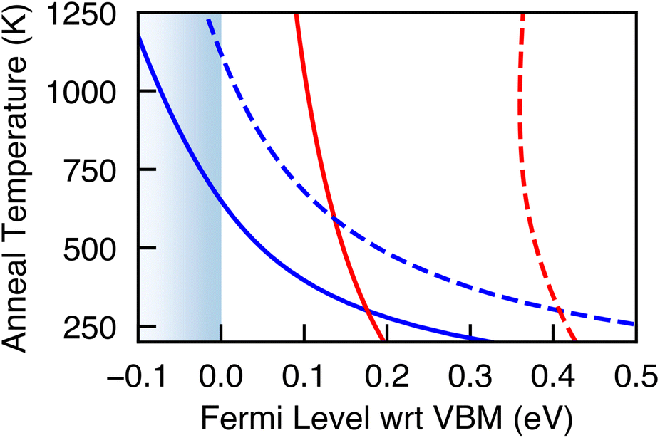 | ||
| Fig. 4 Position of the Fermi level during annealing (red) and quenching (blue) under Cu-poor (solid line) and Cu-rich (dashed line) synthesis conditions. | ||
The DFT supercell approach for calculating defects fails to properly model the bound states of resonant/shallow defects, as their large, delocalized wave functions extend far beyond the supercell length.38–41 Thus constraining these states to the supercell results in strong finite-size effects and spurious exciton-like interactions. However, several indicators can be used to determine that the defect is a true shallow state. For instance, we find the charge density of the V0Cu hole state to be delocalized across the supercell (ESI Section 5†), that the calculated (0/−1) transition level shifts toward the VBM with increasing supercell size, and lastly, that the atomic sites surrounding the vacancy differ in position by less than 0.01 Å between V−1Cu and V0Cu. Indeed, using the screening methods developed by Kumagai et al.,42 we find the V0Cu hole state to have similar orbital character to the bulk VBM, demonstrating its hydrogenic perturbed host state (PHS) nature. Therefore, despite the large predicted concentrations for copper vacancies (Table 2), their shallow nature means they will not play a role in non-radiative capture processes.32
The lowest formation energy n-type defect is Cui. There are four distinct interstitial sites, with the lowest energy site having the deepest (+/0) donor level, 0.17 eV below the CBM. As a result, Cui may trap charge carriers, however the impact on device performance is expected to be limited due to slow hole capture.43,44
VSe is an ultra-deep donor, with transitions levels lying below the VBM – aided by the high energy of the VBM due to Cu d–Se p repulsion, as observed in Cu2ZnSnSe4 (CZTSe).45 While this defect forms in relatively high concentrations under Cu-rich conditions, due to being electronically inactive it should not contribute to non-radiative recombination. The SeSi antisite defect also has ultra-deep donor states in the valence band, however the defect is additionally found to be stable in the −1 and −2 charge states deep in the band gap. Notably, symmetry-breaking was required to identify the ground-state structures of both VSe and SeSi (Fig. S11 and S13†). To stabilize the negative charge states of SeSi the defect undergoes a significant structural relaxation. The SeSi defect moves away from the tetrahedrally bonded cation site and forms a trimer with two of the neighboring Se, similar to the reconstructions observed in Sb2Se3.46 As a result, this defect site could act as a non-radiative recombination center, however to quantitatively determine its impact, this would require the calculation of its carrier capture cross-section.32
The remaining defect states with a formation energy below 1.5 eV, which will form in significant concentrations depending on the growth conditions, are the CuSi antisite and VSi. These defects behave similarly due to the ShakeNBreak47,48 method finding that the lowest energy configuration of a VSi defect is actually a CuSi + VCu complex. This rearrangement occurs due to the high SiIV oxidation state, resulting in it being unfavorable to leave the site unoccupied and the low energy of formation of a VCu leading to a mobile cation. Thus, both CuSi and VSi defects have similar deep-lying levels. However, the carrier capture cross-sections are expected to be very small due to weak structural relaxation between defect charge states, with the bonds surrounding the defect site distorting by less than 0.02 Å upon charge capture/emission. The lack of distortion between charge states can be explained by considering the orbital make-up of the valence band and CuSi. As Cu and Si are tetrahedrally-coordinated by Se, this gives rise to the same Cu d–Se p antibonding interaction as found at the VBM. Thus in the fully-ionised charge state (Cu−3Si), the occupied anti-bonding defect levels lie above the VBM due to Coulomb repulsion, resulting in deep transition levels. Consequently, it is favorable to remove electrons and depopulate the anti-bonding levels, placing holes in the Cu d–Se p states (ESI Fig. S10†). The reduction in charge lowers the energy of the defect states, resulting in them being more VBM-like and making q = 0, −1 and −2 the stable charge states for CuSi.
Overall, our results find the formation energy of antisite defects to be significantly larger than in CIGS and kesterite materials (e.g. CuZn defects has a formation energy of 0.4 eV in CZTS), due to larger valence and size differences between the cation species (i.e. SiIV (r = 0.26 Å) and CuI (r = 0.6 Å) vs. SnIV (r = 0.55 Å) and ZnII (r = 0.6 Å) in CZTS, where SnZn are the killer defects).36,49,50 This would have the added benefit of reducing cation disorder in Cu2SiSe3 which has been shown to lower the formation energy of defects in CZTS.13 All remaining defect species not discussed in detail have too high formation energies to form in sufficient concentrations to significantly affect device performance. Our study of the intrinsic defect in Cu2SiSe3 shows that the antibonding VBM, often associated with defect-tolerance, indeed contributes to the formation of electrically benign defects,51 borne out by the VCu and VSe discussed earlier. This paints a promising picture for potential defect tolerance in this compound.
3 Conclusion
In this work, we have investigated Cu2SiSe3 as a candidate photovoltaic absorber, determining its bandgap to be 1.52 eV using HSE06. A maximum efficiency of 30% at the radiative limit is predicted for thin film devices, and we expect current copper-chalcogenide device architectures to be readily transferable. Using hybrid density functional theory, all intrinsic defect sites were investigated, with the lowest energy defects (VCu and Cui) expected to be benign with respect to carrier recombination. As a result, Cu2SiSe3 shows great promise as a potential defect-tolerant photovoltaic absorber, however further calculations of capture cross-sections are required. We believe this work serves as a promising outlook on the potential solar cell application of this material, and hope that it encourages experimentalists working in the field of emerging photovoltaics to synthesize and investigate Cu2SiSe3 devices.4 Methods
All calculations were performed using periodic DFT within the Vienna Ab Initio Simulation Package (VASP).52–54 This work uses the HSE06 hybrid DFT functional which combines 75% exchange and 100% of the correlation energy from the Perdew, Burke, and Ernzerhof (PBE) semi-local functional with 25% exact Hartree–Fock (HF) exchange at short ranges.17,18,55 HSE06 has been shown to accurately reproduce the electronic structure and properties of many small bandgap semiconductors, including Cu-multinary chalcogenide semiconductors.21 A plane wave energy cutoff of 350 eV was used and k-points were sampled with a Γ centered 4 × 4 × 4 mesh for the 12-atom primitive cell. The total energy was converged to less than 1 meV per atom with these parameters, and a force tolerance of 0.01 eV Å−1 was used during geometry relaxation. The plane wave cutoff was increased to 500 eV during structural relaxation to avoid errors arising from Pulay stress. A denser 6 × 6 × 6 k-point mesh was used for the calculation of the optical properties, and a larger number of unoccupied bands were included in the calculation (NBANDS increased to 100). Upper limits to the photovoltaic efficiency were determined from the HSE06 electronic and optical calculations, using both the ‘Spectroscopic Limited Maximum Efficiency’ (SLME) metric and the method of Blank et al.28,29 To calculate the electronic band alignment, the core level alignment method was used with surfaces generated by surface.56,57Defect calculations were performed in a 96-atom supercell created by the expansion of the primitive unit cell with the matrix:

 | (1) |
Defect concentrations were determined through the calculation of the self-consistent Fermi level as implemented in py-sc-fermi.62,63 Typically materials are grown/annealed at elevated temperatures (as is the case for Cu2SiSe3 (ref. 19, 23 and 64)), where defects form, before cooling to room temperature. Thus, to simulate. Thus, to simulate annealing and quenching, the equilibrium defect concentrations are calculated self-consistently at various annealing temperatures. Next, to simulate quenching the sample to room temperature, the calculated defect concentrations are held constant, while the charge states and Fermi level are allowed to re-equilibrate at 300 K. A schematic outlining the workflow is included in the ESI (Fig. S7†).
Many-body perturbation theory calculations were performed within the Questaal package,65 using the QSGW method of Kotani et al.66 together with the modification to include ladder diagrams within the screened Coulomb interaction W, herein referred to as QSGŴ.67,68 The HSE06 ground state structure was used throughout. Muffin tin radii of 2.37 a.u., 2.07 a.u., and 2.17 a.u. were used for Cu, Si and Se respectively, with an l-cutoff of 4 used for all atoms. A k-mesh of 4 × 4 × 4 and a G-cutoff for the interstitial plane waves of 8.0 Ry½ was used for the convergence of the QSGW and QSGŴ self-energies, with a finer 8 × 8 × 7 mesh used for intermediate DFT calculations. The QSGŴ band gap was found to converge to within 0.01 eV using 12 occupied and 12 empty bands, while a finer 6 × 6 × 6 was used for the solution of the Bethe–Salpeter Equation and the resultant dielectric spectrum.
Conflicts of interest
There are no conflicts to declare.Acknowledgements
We acknowledge Bodoo Batnaran for sharing data which was useful for comparisons in the early stages of this project. A. N and S. R. K acknowledge the EPSRC and SFI Centre for Doctoral Training in Advanced Characterisation of Materials (EP/S023259/1) for funding a PhD studentship. C. N. S. is grateful to the Department of Chemistry at UCL and the Ramsay Memorial Fellowship Trust for the funding of a Ramsay Fellowship. The authors acknowledge the use of the UCL Kathleen and Thomas High Performance Computing Facility. Via membership of the UK's HEC Materials Chemistry Consortium, which is funded by the EPSRC (EP/L000202, EP/R029431, EP/T022213), this work used the ARCHER2 UK National Supercomputing Service (http://www.archer2.ac.uk/) and the UK Materials and Molecular Modelling (MMM) Hub (Thomas – EP/P020194 & Young – EP/T022213).Notes and references
- K. Momma and F. Izumi, J. Appl. Crystallogr., 2008, 41, 653–658 CrossRef CAS.
- A. M. Ganose, A. J. Jackson and D. O. Scanlon, J. Open Source Softw., 2018, 3, 717 CrossRef.
- IPCC, Climate Change 2022: Mitigation of Climate Change. Contribution of Working Group III to the Sixth Assessment Report of the Intergovernmental Panel on Climate Change, Cambridge University Press, Cambridge, UK and New York, NY, USA, 2022, DOI:10.1017/9781009157926.
- Y.-T. Huang, S. R. Kavanagh, D. O. Scanlon, A. Walsh and R. L. Z. Hoye, Nanotechnology, 2021, 32, 132004 CrossRef CAS PubMed.
- S. Hadke, M. Huang, C. Chen, Y. F. Tay, S. Chen, J. Tang and L. Wong, Chem. Rev., 2022, 122(11), 10170–10265 CrossRef CAS PubMed.
- K. V. Sopiha, C. Comparotto, J. A. Márquez and J. J. S. Scragg, Adv. Opt. Mater., 2022, 10, 2101704 CrossRef CAS.
- A. M. Ganose, C. N. Savory and D. O. Scanlon, Chem. Commun., 2016, 53, 20–44 RSC.
- R. Nie, R. R. Sumukam, S. H. Reddy, M. Banavoth and S. I. Seok, Energy Environ. Sci., 2020, 13, 2363–2385 RSC.
- S. Chen, X. G. Gong, A. Walsh and S.-H. Wei, Appl. Phys. Lett., 2010, 96, 021902 CrossRef.
- S. Kim, J. A. Márquez, T. Unold and A. Walsh, Energy Environ. Sci., 2020, 13, 1481–1491 RSC.
- S. Schorr, G. Gurieva, M. Guc, M. Dimitrievska, A. Pérez-Rodríguez, V. Izquierdo-Roca, C. S. Schnohr, J. Kim, W. Jo and J. M. Merino, J. Phys.: Energy, 2019, 2, 012002 Search PubMed.
- L. L. Baranowski, P. Zawadzki, S. Lany, E. S. Toberer and A. Zakutayev, Semicond. Sci. Technol., 2016, 31, 123004 CrossRef.
- W. Chen, D. Dahliah, G.-M. Rignanese and G. Hautier, Energy Environ. Sci., 2021, 14, 3567–3578 RSC.
- Y. Zhang, Y. Wang, J. Zhang, L. Xi, P. Zhang and W. Zhang, J. Chem. Phys., 2016, 144, 194706 CrossRef PubMed.
- D. Dahliah, G. Brunin, J. George, V.-A. Ha, G.-M. Rignanese and G. Hautier, Energy Environ. Sci., 2021, 14, 5057–5073 RSC.
- B. Pamplin, Prog. Cryst. Growth Charact., 1980, 3, 179–192 CrossRef CAS.
- J. Heyd, G. E. Scuseria and M. Ernzerhof, J. Chem. Phys., 2003, 118, 8207–8215 CrossRef CAS.
- A. V. Krukau, O. A. Vydrov, A. F. Izmaylov and G. E. Scuseria, J. Chem. Phys., 2006, 125, 224106 CrossRef PubMed.
- X.-a. Chen, H. Wada, A. Sato and H. Nozaki, J. Alloys Compd., 1999, 290, 91–96 CrossRef CAS.
- F. Oba and Y. Kumagai, Appl. Phys. Express, 2018, 11, 060101 CrossRef.
- Q. Wang, H. Ma, B. Ni, Y. Li, S. Huang, W. Lin and Y. Zhang, J. Phys. Chem. C, 2022, 126, 4684–4697 CrossRef CAS.
- S. R. Kavanagh, C. N. Savory, S. M. Liga, G. Konstantatos, A. Walsh and D. O. Scanlon, J. Phys. Chem. Lett., 2022, 10965–10975 CrossRef CAS PubMed.
- H. ElAnzeery, M. Buffière, K. B. Messaoud, S. Oueslati, G. Brammertz, O. E. Daif, D. Cheyns, R. Guindi, M. Meuris and J. Poortmans, Phys. Status Solidi – Rapid Res. Lett., 2015, 9, 338–343 CrossRef CAS.
- A. Zakutayev, C. M. Caskey, A. N. Fioretti, D. S. Ginley, J. Vidal, V. Stevanovic, E. Tea and S. Lany, J. Phys. Chem. Lett., 2014, 5, 1117–1125 CrossRef CAS PubMed.
- S. B. Zhang, S.-H. Wei, A. Zunger and H. Katayama-Yoshida, Phys. Rev. B: Condens. Matter Mater. Phys., 1998, 57, 9642–9656 CrossRef CAS.
- A. Walsh and A. Zunger, Nat. Mater., 2017, 16, 964–967 CrossRef CAS PubMed.
- Y.-T. Huang, S. R. Kavanagh, M. Righetto, M. Rusu, I. Levine, T. Unold, S. J. Zelewski, A. J. Sneyd, K. Zhang, L. Dai, A. J. Britton, J. Ye, J. Julin, M. Napari, Z. Zhang, J. Xiao, M. Laitinen, L. Torrente-Murciano, S. D. Stranks, A. Rao, L. M. Herz, D. O. Scanlon, A. Walsh and R. L. Z. Hoye, Nat. Commun., 2022, 13, 4960 CrossRef CAS PubMed.
- L. Yu and A. Zunger, Phys. Rev. Lett., 2012, 108, 068701 CrossRef PubMed.
- B. Blank, T. Kirchartz, S. Lany and U. Rau, Phys. Rev. Appl., 2017, 8, 024032 CrossRef.
- S. Chen, A. Walsh, J.-H. Yang, X. G. Gong, L. Sun, P.-X. Yang, J.-H. Chu and S.-H. Wei, Phys. Rev. B: Condens. Matter Mater. Phys., 2011, 83, 125201 CrossRef.
- R. K. Swank, Phys. Rev., 1967, 153, 844–849 CrossRef CAS.
- A. Alkauskas, Q. Yan and C. G. Van de Walle, Phys. Rev. B: Condens. Matter Mater. Phys., 2014, 90, 075202 CrossRef CAS.
- A. Alkauskas, M. D. McCluskey and C. G. Van de Walle, J. Appl. Phys., 2016, 119, 181101 CrossRef.
- S. R. Kavanagh, D. O. Scanlon, A. Walsh and C. Freysoldt, Faraday Discuss., 2022, 239, 339–356 RSC.
- S. R. Kavanagh, A. Walsh and D. O. Scanlon, ACS Energy Lett., 2021, 6, 1392–1398 CrossRef CAS PubMed.
- C. Persson, Y.-J. Zhao, S. Lany and A. Zunger, Phys. Rev. B: Condens. Matter Mater. Phys., 2005, 72, 035211 CrossRef.
- C. Rincón and R. Márquez, J. Phys. Chem. Solids, 1999, 60, 1865–1873 CrossRef.
- S. Lany and A. Zunger, J. Appl. Phys., 2006, 100, 113725 CrossRef.
- G. Zhang, A. Canning, N. Grønbech-Jensen, S. Derenzo and L.-W. Wang, Phys. Rev. Lett., 2013, 110, 166404 CrossRef PubMed.
- Y. Zhang, A. Mascarenhas and L.-W. Wang, Phys. Rev. B: Condens. Matter Mater. Phys., 2006, 74, 041201 CrossRef.
- M. W. Swift, H. Peelaers, S. Mu, J. J. L. Morton and C. G. Van de Walle, npj Comput. Mater., 2020, 6, 1–9 CrossRef.
- Y. Kumagai, N. Tsunoda, A. Takahashi and F. Oba, Phys. Rev. Mater., 2021, 5, 123803 CrossRef CAS.
- W. Shockley and W. T. Read, Phys. Rev., 1952, 87, 835–842 CrossRef CAS.
- R. N. Hall, Phys. Rev., 1952, 87, 387 CrossRef CAS.
- S. Kim, J.-S. Park and A. Walsh, ACS Energy Lett., 2018, 3, 496–500 CrossRef CAS.
- X. Wang, S. R. Kavanagh, D. O. Scanlon and A. Walsh, Four-Electron Negative-U Vacancy Defects in Antimony Selenide, 2023, http://arxiv.org/abs/2302.04901 Search PubMed.
- I. Mosquera-Lois, S. R. Kavanagh, A. Walsh and D. O. Scanlon, J. Open Source Softw., 2022, 7, 4817 CrossRef.
- I. Mosquera-Lois, S. R. Kavanagh, A. Walsh and D. O. Scanlon, npj Comput. Mater., 2023, 9, 1–11 CrossRef.
- R. D. Shannon, Acta Crystallogr., Sect. A: Cryst. Phys., Diffr., Theor. Gen. Crystallogr., 1976, 32, 751–767 CrossRef.
- S. Kim, J.-S. Park, S. N. Hood and A. Walsh, J. Mater. Chem. A, 2019, 7, 2686–2693 RSC.
- R. E. Brandt, J. R. Poindexter, P. Gorai, R. C. Kurchin, R. L. Z. Hoye, L. Nienhaus, M. W. B. Wilson, J. A. Polizzotti, R. Sereika, R. Žaltauskas, L. C. Lee, J. L. MacManus-Driscoll, M. Bawendi, V. Stevanović and T. Buonassisi, Chem. Mater., 2017, 29, 4667–4674 CrossRef CAS.
- G. Kresse and J. Hafner, Phys. Rev. B: Condens. Matter Mater. Phys., 1993, 47, 558–561 CrossRef CAS PubMed.
- G. Kresse and J. Furthmüller, Phys. Rev. B: Condens. Matter Mater. Phys., 1996, 54, 11169–11186 CrossRef CAS PubMed.
- G. Kresse and D. Joubert, Phys. Rev. B: Condens. Matter Mater. Phys., 1999, 59, 1758–1775 CrossRef CAS.
- J. P. Perdew, K. Burke and Y. Wang, Phys. Rev. B: Condens. Matter Mater. Phys., 1996, 54, 16533–16539 CrossRef CAS PubMed.
- S.-H. Wei and A. Zunger, Appl. Phys. Lett., 1998, 72, 2011–2013 CrossRef CAS.
- K. Brlec, D. W. Davies and D. O. Scanlon, J. Open Source Softw., 2021, 6, 3171 CrossRef.
- A. Kononov, C.-W. Lee, E. P. Shapera and A. Schleife, J. Phys.: Condens. Matter, 2023, 35, 334002 CrossRef PubMed.
- Y. Kumagai and F. Oba, Phys. Rev. B: Condens. Matter Mater. Phys., 2014, 89, 195205 CrossRef.
- C. Freysoldt, J. Neugebauer and C. G. Van de Walle, Phys. Rev. Lett., 2009, 102, 016402 CrossRef PubMed.
- C. G. Van de Walle and J. Neugebauer, J. Appl. Phys., 2004, 95, 3851–3879 CrossRef CAS.
- J. Buckeridge, Comput. Phys. Commun., 2019, 244, 329–342 CrossRef CAS.
- A. G. Squires, D. O. Scanlon and B. J. Morgan, J. Open Source Softw., 2023, 8(82), 4962 CrossRef.
- G. Brammertz, B. Vermang, H. ElAnzeery, S. Sahayaraj, S. Ranjbar, M. Meuris and J. Poortmans, Phys. Status Solidi C, 2017, 14, 1600162 CrossRef.
- D. Pashov, S. Acharya, W. R. Lambrecht, J. Jackson, K. D. Belashchenko, A. Chantis, F. Jamet and M. van Schilfgaarde, Comput. Phys. Commun., 2020, 249, 107065 CrossRef CAS.
- T. Kotani, M. van Schilfgaarde and S. V. Faleev, Phys. Rev. B: Condens. Matter Mater. Phys., 2007, 76, 165106 CrossRef.
- B. Cunningham, M. Grüning, P. Azarhoosh, D. Pashov and M. van Schilfgaarde, Phys. Rev. Mater., 2018, 2, 034603 CrossRef CAS.
- B. Cunningham, M. Grüning, D. Pashov and M. van Schilfgaarde, QSGŴ: Quasiparticle Self consistent GW with ladder diagrams in W, arXiv, 2023, preprint, arXiv:2302.06325v1 [cond-mat.mtrl-sci], DOI:10.48550/arXiv.2302.06325.
Footnotes |
| † Electronic supplementary information (ESI) available: Additional figures describing the electronic structure, defect formation energies, energy lowering distortions, and discussion on the chemical potential space. See DOI: https://doi.org/10.1039/d3ta02429f |
| ‡ Calculation data is provided in an online repository at https://doi.org/10.5281/zenodo.7611652 |
| This journal is © The Royal Society of Chemistry 2023 |