
 Open Access Article
 This Open Access Article is licensed under a Creative Commons Attribution-Non Commercial 3.0 Unported Licence
Harnessing the unusually strong improvement of thermoelectric performance of AgInTe2 with nanostructuring†
Jose J.
Plata
 *a,
Ernesto J.
Blancas
a,
Antonio M.
Márquez
a,
Victor
Posligua
b,
Javier
Fdez Sanz
a and
Ricardo
Grau-Crespo
c
*a,
Ernesto J.
Blancas
a,
Antonio M.
Márquez
a,
Victor
Posligua
b,
Javier
Fdez Sanz
a and
Ricardo
Grau-Crespo
c
aDepartamento de Química Física, Universidad de Sevilla, Seville, Spain. E-mail: jplata@us.es
bDepartment of Chemistry, Imperial College London, Molecular Sciences Research Hub, London, UK
cDepartment of Chemistry, University of Reading, Reading, UK
First published on 20th July 2023
Abstract
Nanostructuring is a well-established approach to improve the thermoelectric behavior of materials. However, its effectiveness is restricted if excessively small particle sizes are necessary to considerably decrease the lattice thermal conductivity. Furthermore, if the electrical conductivity is unfavorably affected by the nanostructuring, it could cancel out the advantages of this approach. Computer simulations predict that silver indium telluride, AgInTe2, is unique among chalcopyrite-structured chalcogenides in requiring only a mild reduction of particle size to achieve a substantial reduction in lattice thermal conductivity. Here, ab initio calculations and machine learning are combined to systematically chart the thermoelectric properties of nanostructured AgInTe2, in comparison with its Cu-based counterpart, CuInTe2. In addition to temperature and doping carrier concentration dependence, ZT is calculated for both materials as functions of the polycrystalline average grain size, taking into account the effect of nanostructuring on both phonon and electron transport. It is shown that the different order of magnitude between the mean free path of electrons and phonons disentangles the connection between the power factor and lattice thermal conductivity when reducing the crystal size. ZT values up to 2 are predicted for p-type AgInTe2 at 700 K when the average grain size is in the affordable 10–100 nm range.
1. Introduction
The recovery of heat as electricity through the use of thermoelectric (TE) materials has attracted the attention of researchers since the Seebeck and Peltier effects were described at the beginning of the 19th century. The increasing global energy demand and the high volatility of the oil and gas markets, together with the fact that 70% of energy produced by our society is wasted as heat, makes the development of thermoelectric materials a pressing societal need. The discovery of more efficient and economical thermoelectric materials remains a challenging task, as does the optimization of existing thermoelectric materials. In recent decades, significant resources have been dedicated to the improvement of the performance of these materials,1 measured by its figure of merit, ZT = S2σT/(κelec + κlatt), where σ is the electrical conductivity, κelec and κlatt are the electrical and lattice thermal conductivities respectively, T is the temperature and S is the Seebeck coefficient. Maximizing ZT is a complex task, as these materials properties are strongly coupled.2 Additionally, the difficulty of establishing robust connections between real-space synthetic variables (temperature, chemical composition, doping concentration or grain size) and reciprocal-space materials properties that modify ZT (scattering times or electronic and vibrational structure) hampers the discovery of new and more efficient thermoelectric materials.Computational materials science has changed this paradigm in the 21st century with the development of methodologies and frameworks to accurately calculate transport properties3–7 and analyze the effect of some variables such as their chemical composition.8 However, predicting the TE performance of bulk single crystal materials through computational screening9 does not guarantee a high efficiency in the final device. TE performance of materials is drastically modified by some variables linked to processing, such as doping concentration or grain size, so candidate materials need to go through an optimization process. Although many strategies such as alloying,10 doping,11 dislocation,12 or phase engineering13,14 have been proposed to enlarge and optimize ZT, they often involve laborious and time-consuming repeated experiments of synthesis, characterization and property measurement. One of the most common strategies is the nanostructuring or nanocrystalization, which was proposed for the first time by Dresselhaus in the 1990s.15 Tailoring the grain size in polycrystalline samples has led to significant improvements of the thermoelectric performance of materials.16,17 For instance, controlling the nanostructure of half-Heusler alloys leads to an enhancement of their power factor, PF = S2σ.18 However, the critical reduction of κlatt plays the dominant role, increasing ZT when grain size is reduced to the nanoscale.19
The effect of the grain size on κlatt mainly depends on the phonon lifetimes, which can present different behaviors even in a set of materials with the same structural prototype. In previous work,20 we reported that the grain size, L0.5, needed to halve the lattice thermal conductivity κlatt across a family of chalcopyrite semiconductors was roughly proportional to the bulk thermal conductivity value (Fig. 1). Considering that trend, AgInTe2 can be identified as an outlier, with an unusual potential to benefit from nanostructuring, in the sense that its κlatt can be reduced to half of its bulk value with a substantially less drastic reduction of grain size, if compared to other Se- and Te-based chalcopyrites with similar bulk conductivities. AgInTe2, CuInTe2 and their alloys have been extensively studied during recent years due to their promising thermoelectric performance. ZT values above 1.5 have been measured for CuInTe2 by domain engineering21 or manipulating localized vibrations of interstitial Te atoms.22 Despite these outstanding values, there is a large variability on the reported figures of merit of these materials due to the strong dependence of this parameter with the chemical nature of the monovalent cation, temperature, carrier concentration and grain size or nanostructure. Here, we present, for first time, a theoretical approach to accurately and systematically explore the multivariate space that defines the TE performance of CuInTe2 and AgInTe2, paying special attention to the role of the grain size in polycrystalline samples and opening the door to perform in silico optimization of TE materials.
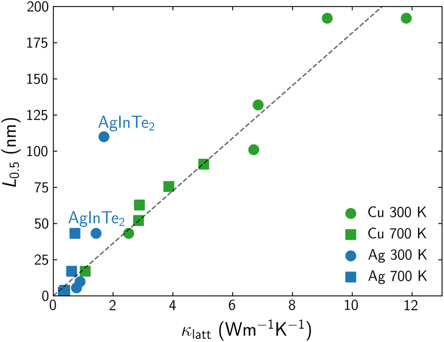 | ||
| Fig. 1 Correlation between L0.5 and bulk κlatt for Cu- (green) and Ag-based (blue) chalcopyrites at 300 K (circles) and 700 K (squares). AgInTe2 outlayer is labeled. Adapted from Plata et al.20 | ||
2. Methodology
2.1 Geometry optimization
CuInTe2 and AgInTe2 chalcopyrite structure were fully relaxed (atoms and lattice) with the VASP package,23,24 using projector-augmented wave (PAW) potentials.25 Energies were obtained using the exchange–correlation functional proposed by Perdew–Burke–Ernzerhof (PBE),26 including Grimme-D3 van der Waals corrections.27 Core and valence electrons were selected following standards proposed by Calderon et al.28 An accurate description of the minimum of the potential energy surface was obtained using a high-energy cut-off of 500 eV and a dense mesh of 4096 k-points per reciprocal atom. Geometry and lattice vectors were fully relaxed, using a 16-atom conventional cell, until forces acting over each atom were smaller than 10−7 eV Å−1. Wave-function was considered converged when the energy difference between two consecutive electronic steps was smaller than 10−9 eV, including an additional support grid for the evaluation of the augmentation charges to reduce the noise in the forces.2.2 Supercell single-point calculations and force constants
HiPhive package was used to calculate interatomic force constants, IFCs, combining the forces calculated for random atomic distortions in supercells with machine learning regression.29,30 The forces were calculated in 18 4 × 4 × 2 supercells (512 atoms) using the same setup as the one used for geometry optimizations. A Monte Carlo algorithm was used to set the amplitude of the distortions applied to each atom, obtaining an average displacement amplitude for each configuration of ∼0.13 Å. The force constants were extracted from a multi-linear regression of the DFT forces, applying the recursive feature elimination, RFE, algorithm. Reducing the number of parameters via RFE also simplifies the model, keeping only the most relevant interaction terms. IFCs were calculated including cutoffs for second, third and fourth-order terms, following the same strategy as in previous work.202.3 Boltzmann transport equation solver
The ShengBTE code is used in order to solve the Boltzmann transport equation, BTE, for phonons and calculate the lattice thermal conductivity, κlatt.31 Scattering times were computed including isotopic and three-phonon scattering effects. Memory demand and the convergence of κlatt with the number of q-points were balanced using a Gaussian smearing of 0.1 and a dense mesh of 20 × 20 × 10 q-points. The value of κlatt for polycrystalline samples with an average grain size of L is approximated as the cumulative contributions from all mean free paths up to L. This strategy has led to a good description of the lattice thermal conductivity of CuGaTe2 and other chalcopyrites.202.4 Electronic transport properties
Electrical conductivity, σ, Seebeck coefficient, S and the electronic contribution to the thermal conductivity, κelec were calculated using the AMSET package.3 This code solves the electronic BTE using the Onsager coefficients to predict electronic transport properties with the wavefunction from a DFT calculation as main input. Scattering rate for each temperature, doping concentration, band, and k-point are calculated including scattering due to deformation potentials, ADPs, piezoelectric interactions, PIEs, polar optical phonons, POPs, and ionized impurities, IMPs. Electronic transport properties were calculated using the primitive cell (8 atoms) and a dense mesh of 10 × 10 × 10 k-points. Polar phonon frequency and elastic constants were calculated using the same setup described previously. Wave-function coefficients and deformation potential were calculated using the HSE06![[thin space (1/6-em)]](https://www.rsc.org/images/entities/char_2009.gif) 32,33 functional in order to obtain an accurate description of the electronic structure. Static dielectric constants were calculated as the sum of the high-frequency dielectric constants and the ionic dielectric constants. Ionic dielectric constants were calculated using density functional perturbation theory.34,35 Due to the strong dependence of the high-frequency dielectric constant with the band gap and thus with the exchange–correlation functional, experimental values reported by Holah36 and Kumar37 were used. Electron scattering at grain boundaries was included as vg/L where vg is the group velocity and L the mean free path.
32,33 functional in order to obtain an accurate description of the electronic structure. Static dielectric constants were calculated as the sum of the high-frequency dielectric constants and the ionic dielectric constants. Ionic dielectric constants were calculated using density functional perturbation theory.34,35 Due to the strong dependence of the high-frequency dielectric constant with the band gap and thus with the exchange–correlation functional, experimental values reported by Holah36 and Kumar37 were used. Electron scattering at grain boundaries was included as vg/L where vg is the group velocity and L the mean free path.
3. Results
The optimization of the TE performance of AgInTe2 and CuInTe2 is performed based on three main variables: temperature, T, carrier concentration, n, and average grain size, L, which can be modified during the synthesis or TE module operation. CuInTe2 and most TE efficient chalcopyrites have been reported as p-type materials; however, AgInTe2 has been described both as p-type and n-type, depending on the crystal growth conditions.38 For this reason, CuInTe2 is explored as a p-type semiconductor, while the TE performance of AgInTe2 is calculated for both p- and n-type carriers.There is very limited information in the literature about the electronic transport properties of AgInTe2, but there are many previous experimental studies of CuInTe2, which therefore will be used to validate our theoretical framework. Electrical conductivity, σ, and Seebeck coefficient, S, are explored in a wide range of temperatures (T = 300–700 K) and carrier concentrations (n = 1017–1020 cm−3). The carrier concentration range has been selected based on the previously reported experimental values for CuInTe2, which is wider than the range for AgInTe2. At 300 K, calculated σ and S present a reasonably good agreement with available experimental data39–48 (Fig. 2). While σ is slightly underestimated at low and medium carrier concentrations (Fig. 2a), S is slightly overestimated (10–15% error) in the whole range of concentrations (Fig. 2b). These deviations cancel each other when the power factor, PF = S2σ, is calculated, with PF deviations being significant only when n > 2 × 1019 cm−3 (Fig. 2c). Putting these discrepancies in context, we note that they are similar to the experimental uncertainty in electric transport measurements. For example, the analysis by Mackey et al.49 of the uncertainty in the measurement of electronic thermoelectric properties based on the four-probe method, found that electrical resistivity measurements contain a 7% uncertainty across any temperature, Seebeck coefficient measurements presents between 1% and 13% uncertainty depending on the temperature, and the power factor has a combined uncertainty of +7.3%/−27%. In addition to the uncertainty on the experimental measurements, part of the discrepancies between calculated and experimental values stem from scattering processes at the point defects created when reaching such high carrier concentrations, which are not included in our theoretical model. In the AMSET code, comparing theoretical predictions and experimental results based on how σ and S change with temperature present some challenges. Carrier concentration increases when temperature is increased, so experimentally, both variables change simultaneously. Based on previous studies,47σ and S have been computed at two different carrier concentrations that would be the upper and lower limits experimentally reported for a specific temperature range. While all experimental σ values between 300 and 500 K are in between the calculated upper and lower limits (inset in Fig. 2a), some of the calculated S at higher temperatures are slightly overestimated, around 7% error (inset in Fig. 2b). When calculated σ and S are combined in the PF, this is in a very good agreement with data for the whole range of temperatures. Experimental PF around 300 K is very close to the calculated lower limit (n = 5 × 1017 cm−3).47 The carrier concentration increases when temperature is raised so experimental PF values close to 500 K are similar to the calculated values, using the upper carrier concentration limit (n = 3 × 1018 cm−3). Overall, the proposed theoretical framework predicts the behavior of the electronic transport properties with a higher accuracy than other approaches. For instance, Wei et al. predicted σ = 3.85 × 10⁴ S m−1 at 300 K and n = 2.69 × 1019 cm−3 which is approximately a 100% error with respect to experimental values.50
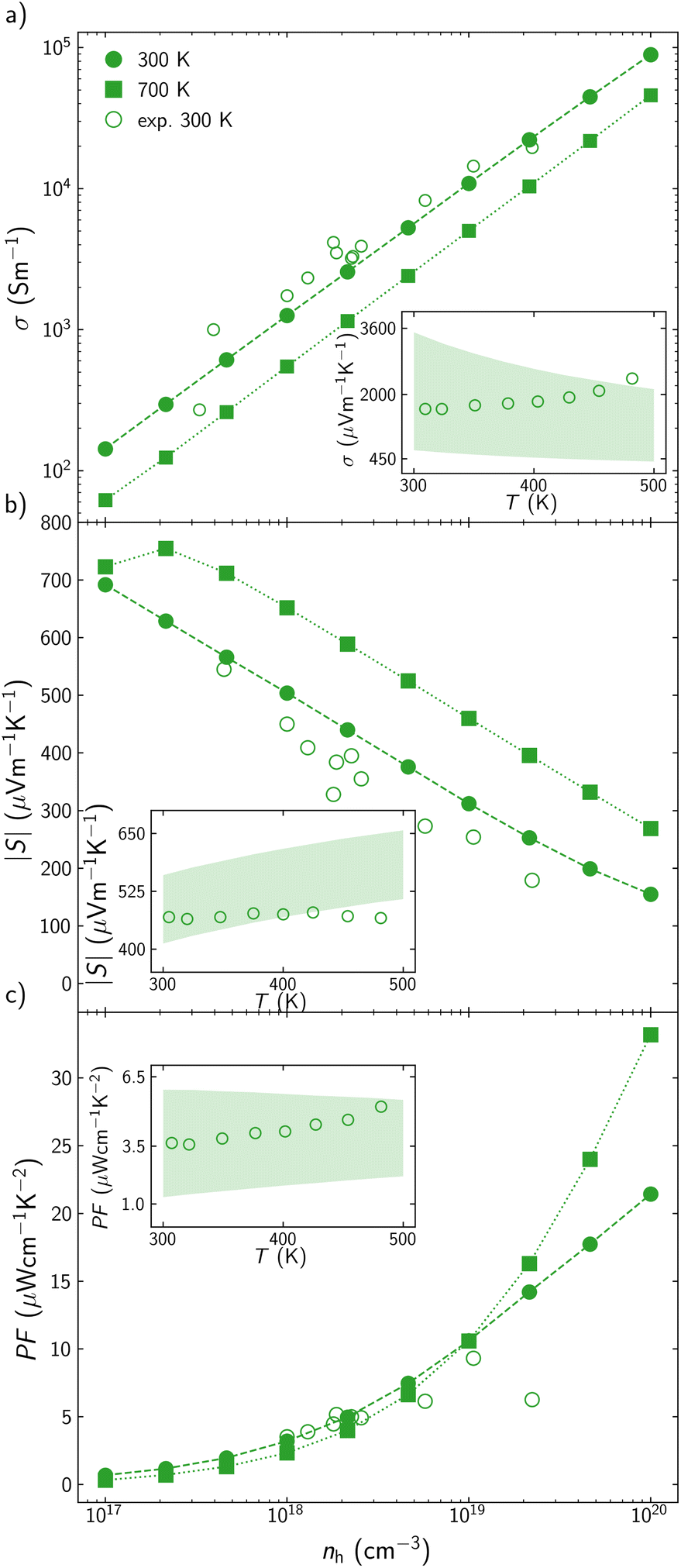 | ||
| Fig. 2 (a) Electrical conductivity, σ, (b) Seebeck coefficient, S, and (c) power factor, PF, for CuInTe2 at different hole concentration, nh, at 300 K (circles) and 700 K (squares). Reported experimental data are represented with empty points.39–48 Inset figures show σ, S, and PF at the 300–500 K interval. Shading area is enclosed by the calculated values using the minimum and maximum experimental carrier concentrations reported for that temperature range.47 | ||
AgInTe2 presents slightly lower σ values than CuInTe2 as p-type semiconductor but around one order of magnitude higher as n-type semiconductor (Fig. 3a). Due to Pisarenko relation, this trend is reverted for S, where p-type AgInTe2 presents higher values than its n-type counterpart (Fig. 3b). These values can be hardly compared with experimental data because most studies did not or could not quantify the carrier concentration of the samples. This fact is in agreement with the extremely low carrier concentration observed in some reports, most of the time below 1017 cm−3.51 However, the experimental S reported by Wang et al. at 700 K46 is in very good agreement with our predictions. Based on these results, it can be concluded that the lower PF observed for AgInTe2 with respect to CuInTe2 as p-type semiconductor stems from the lower carrier concentration of the material and not because of their electronic transport properties by themselves (Fig. 3c). Moreover, n-type AgInTe2 presents higher PF than its p-type counterpart at low and medium carrier concentration values, being more accessible from a synthetic point of view (Fig. 3c).
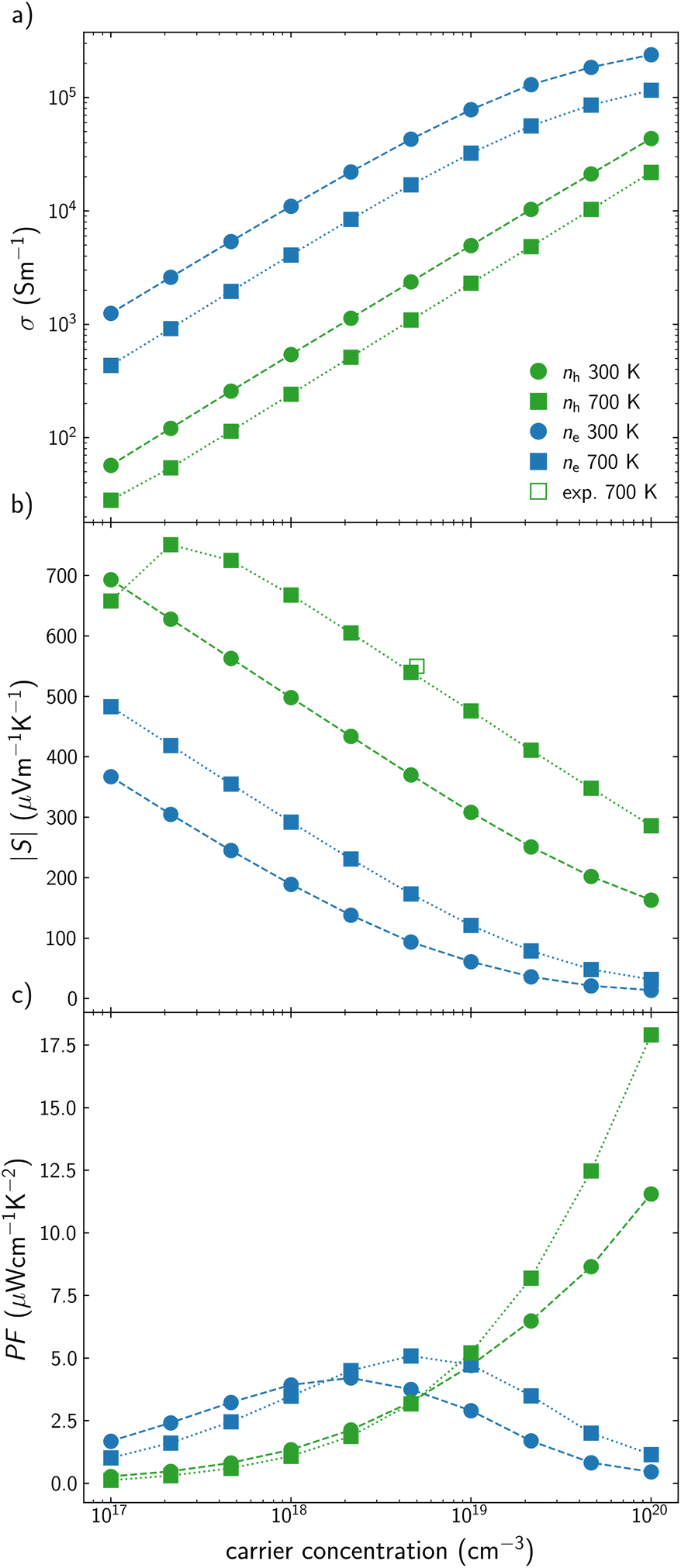 | ||
| Fig. 3 (a) Electrical conductivity, σ, (b) Seebeck coefficient, S, and (c) power factor, PF, for AgInTe2 at different carrier concentration, n, at 300 K (circles) and 700 K (squares). Green and blue are used for p-type and n-type conduction, respectively. Reported experimental data46 are represented with empty points. | ||
At low carrier concentrations, the semiconductor nature of CuInTe2 and AgInTe2 makes the lattice thermal conductivity, κlatt, the main contributor to κ in the whole range of explored temperatures. Comparing κlatt obtained through the solution of the BTE with experiment is always a challenging task. Experimental samples are usually polycrystalline, which reduces the κlatt due to the phonon scattering processes at the grain boundaries. Additionally, the defects connected to carriers (holes or electrons) also act as phonon scattering centers, reducing κlatt. For instance, Yan et al. and Liu et al. have synthesized polycrystalline CuInTe2 samples with similar micro-metric size but different carrier concentration at 300 K, 1.8 × 1018 cm−3 and 1.06 × 1019 cm−3, respectively. The samples with higher carrier concentration (and point defects) present values for κlatt around a 10% lower than the sample with lower carrier concentration. Our theoretical model does not explicitly include grain boundaries or point defects when calculating bulk κlatt, which is why our calculated values slightly overestimate experimental results (Fig. 4a). This overestimation is larger at high temperatures because (i) carrier concentration and point defects are increased with temperatures and (ii) 4th-order scattering processes contribute to κlatt but are not included in the solution of the BTE.55,56 Although a similar trend was found for AgInTe2, the overestimation of the calculated values is considerably lower if compared with the CuInTe2 results (Fig. 4b). This is partially due to the more than three times lower κlatt found for AgInTe2 with respect to CuInTe2.
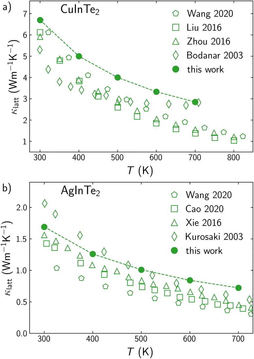 | ||
| Fig. 4 Temperature variation of lattice thermal conductivity, κlatt, for (a) CuInTe2 and (b) AgInTe2. Calculated values are represented with filled points while experimental values are depicted with empty points.46,47,52–54 | ||
The improvement of ZT by fine-tuning the carrier concentration is hampered by physical laws that interconnect TE properties. For instance, Pisarenko plots show how there are limitations in the enlargement of S and σ simultaneously. Nanostructuring introduces a new variable, length scale, that permits the decoupling of the properties that govern thermoelectricity. The effect of the average grain size of a polycrystalline sample, L, on the transport properties of CuInTe2 and AgInTe2 is included in Fig. 5. Due to the low influence of L on S, we will focus on analyzing the behavior of PF and κlatt, using two different temperatures (300 and 700 K) and a moderate carrier concentration of 4.64 × 1018 cm−3. PF of p-type CuInTe2 is reduced around a 5% when L is below 100 nm and between 25% and 32% when L is below 10 nm depending on the temperature (Fig. 5a). This trend is similar for p-type AgInTe2, where PF is reduced around 2% when L is below 100 nm and between 15% and 25% when L is below 10 nm (Fig. 5b). The reduction of PF with L for n-type AgInTe2 is slightly different, decreasing around 10% when L is below 100 nm and between 50% and 80% when L is below 10 nm (Fig. 5b). These results should be analyzed based on the mean free path, MFP, of the carriers (see inset in Fig. 5a). Valence band MFPs for CuInTe2 are mostly below 40 nm at 300 K which explains the low reduction of PF above 100 nm. MFP values for AgInTe2 valence band are even lower at 300 K so PF is only effectively reduced below 20 nm. However, n-type AgInTe2 presents a more drastic reduction of PF when grain size is below 400 nm because conduction band MFP values are considerably larger for both CuInTe2 and AgInTe2 than the valence band MFP values. Lattice thermal conductivity seems to be more sensitive to nanostructuring than PF (Fig. 5c and d). Both CuInTe2 and AgInTe2 present an approximate 50% reduction on κlatt around 100 nm at 300 K. Unfortunately, κlatt tuning at 700 K requires smaller grain sizes, with L0.5 values around 30–40 nm. The drastic modification of κlatt when average grain size is reduced from few micrometers to 100 nm is considerably larger than the κlatt reduction experimentally observed by doping and discussed in the previous section, which confirms that grain boundary effects are the main cause of departure from ideal bulk behavior.
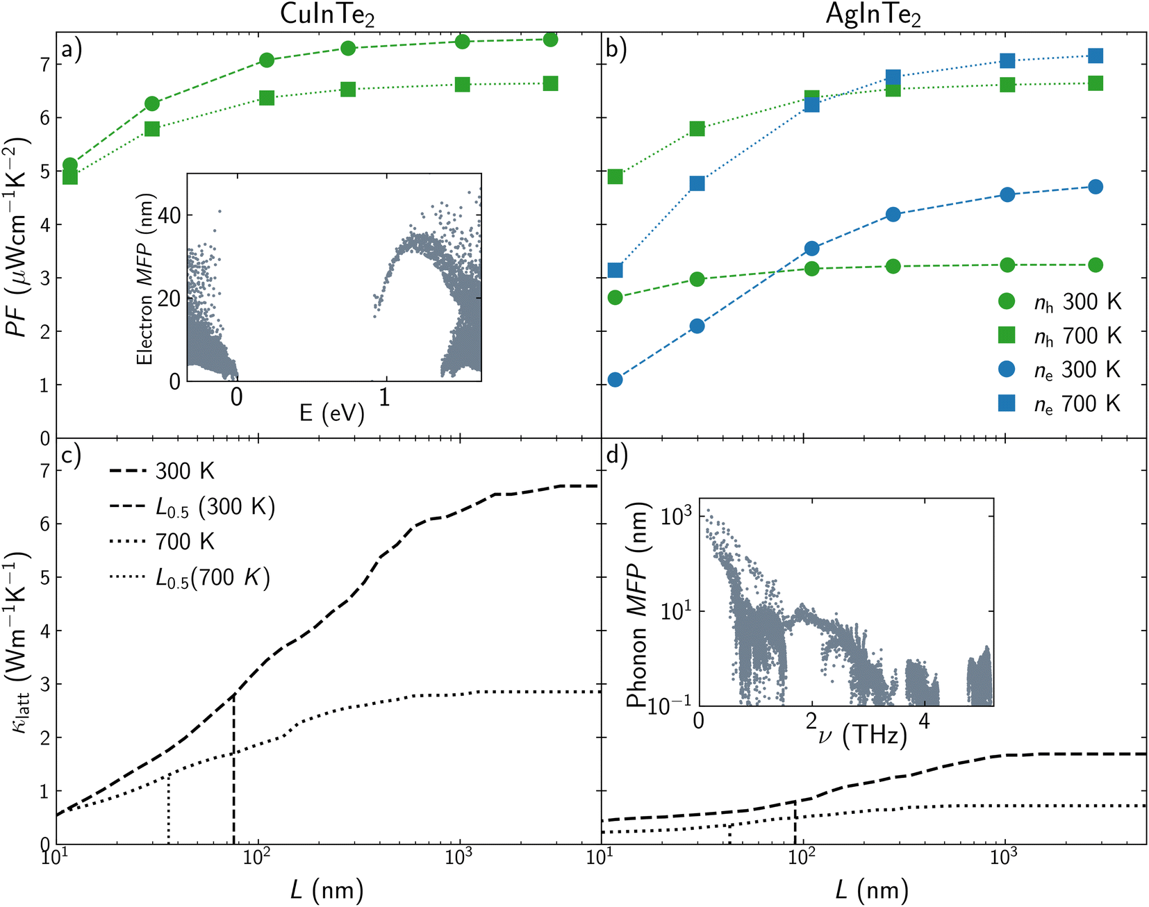 | ||
| Fig. 5 Power factor, PF, dependence with the grain average size for (a) CuInTe2 and (b) AgInTe2 at n = 4.64 × 1018 cm−3. Circles and squares are used for 300 K and 700 K, respectively. Green and blue colors are used for p-type and n-type semiconductors, respectively. The inset in panel (a) shows the electron mean free path, MFP, for p-type CuInTe2 at 300 K. Lattice thermal conductivity, κlatt, dependence with the grain size for (c) CuInTe2 and (d) AgInTe2 at 300 K (dashed line) and 700 K (dotted line). Vertical lines represent the grain size, L0.5, in which κlatt have been reduced a 50% with respect to the single crystal value. The inset in panel (d) shows the phonon mean free path, MFP, for p-type AgInTe2 at 300 K. | ||
Similarly to holes and electrons, phonon MFP is the property governing this behavior. The most important contributions to κlatt stem from acoustic and low-frequency optical modes (Fig. S2†), so examining their MFPs values is the key to understand the thermal conductivity behavior. The MFPs of acoustic modes around Γ are larger for CuInTe2 than for AgInTe2, which is why κlatt for CuInTe2 is reduced even with large grain size above 1 μm (see inset at Fig. 5d). However, MFP values for both materials are moderately high in the range of 0–1 THz so their κlatt drastically decrease when particle size is reduced in the range of 1 μm–100 nm. The origin of these large MFP is linked to the high group velocities and low scattering rates of the acoustic modes (Fig. S2†). This behavior is less pronounced at high temperatures where scattering times and MFPs are shorter.
Once electronic and phonon transport properties have been predicted, the thermoelectric figure of merit, ZT, can be studied considering temperature, carrier concentration and grain size as main variables. Contour plot – heat maps shows how ZT increases with temperature in the explored range for both materials (Fig. 6a, c and e). This is not the case for carrier concentration. While ZT for p-type CuInTe2 and AgInTe2 increases monotonically with the carrier concentration (Fig. 6a and c), ZT for n-type AgInTe2 presents a maximum between n = 2.5 × 10¹⁸ and 5 × 1018 cm−3 (Fig. 6e), which is connected to its PF as was described above. These results cannot be compared with experimental values because, although experimental ZT values are reported at specific temperatures, it is not common that the carrier concentration of the samples are measured beyond 300 K. Cao et al. found that the carrier concentration of CuInTe2 at 600 K is close to 1019 cm−3 so it can be assumed that n > 1019 cm−3 at 700 K. Our predictions for CuInTe2 show ZT values between 0.38 and 0.65 at 700 K and n > 1019 cm−3 which is in very good agreement with experimental reports whose values range between 0.35 and 0.6. Similarly, Wang et al. reported a ZT of 0.18 at 700 K and n = 3.4 × 1018 cm−3 for AgInTe2, which match well with our prediction of ZT = 0.24. Although the accuracy of the model is demonstrated, it is necessary to discuss if the optimized parameters are accessible from an experimental point of view. Controlling experimentally the carrier concentration to optimize the TE performance of materials is not a trivial task. In addition to the study presented in this work, an accurate thermodynamic analysis to define the dopability window of the material should be performed to establish whether the optimal conditions can be experimentally achieved. Recently, Adamczyk et al. have explored the dopability of CuInTe2 (ref. 57) and AgInTe2.58 This information is particularly critical for AgInTe2 because previous experimental work had reported very low carrier concentration, well below the optimal calculated concentrations which are above 1019 cm−3 at 700 K. Promisingly, Adamczyk et al. found p-type AgInTe2 samples with carrier concentrations around 1018 cm−3 at 323 K which were synthesized at In- and Te-rich conditions. These results suggest that it might be possible to achieve carrier concentrations near the optimal value above 1019 cm−3 at 700 K for p-type AgInTe2 in order to maximize ZT.
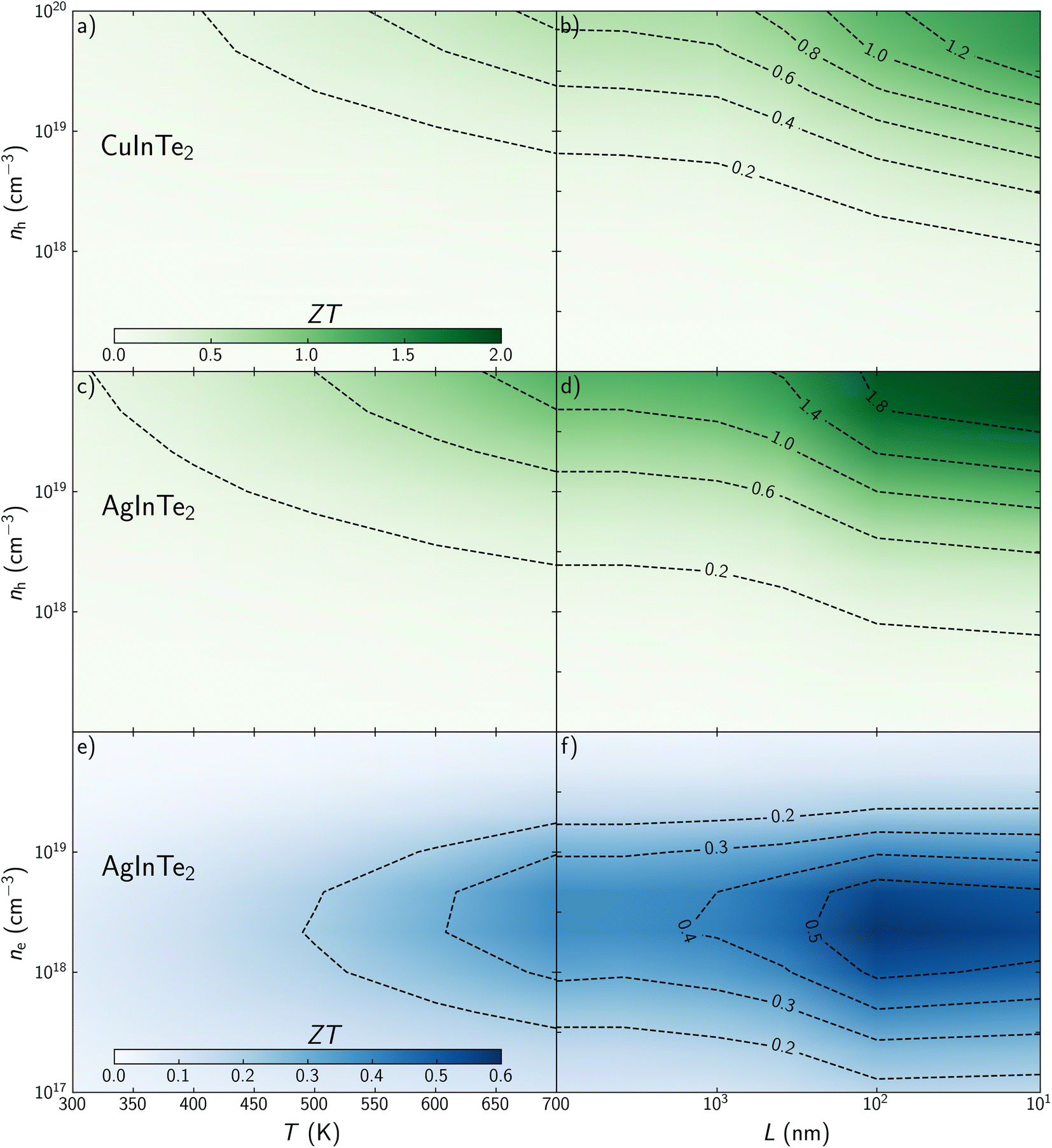 | ||
| Fig. 6 Thermoelectric figure of merit, ZT, dependence on temperature, T, and carrier concentration, n for (a) p-type CuInTe2, (c) p-type AgInTe2 and (e) n-type AgInTe2 single crystals. ZT dependence on average grain size, L, and carrier concentration, n for (b) p-type CuInTe2, (d) p-type AgInTe2 and (f) n-type AgInTe2 polycrystalline samples at 700 K. | ||
To the best of our knowledge, most previous experimental work refers to polycrystalline samples, where grains are in the range of several micrometers, so ZT is barely affected by their size. Nanostructuring effects on ZT were explored at 700 K for both materials. Overall, reducing the grain size at nanoscale drastically improves the TE performance of CuInTe2 and AgInTe2 (Fig. 6b, d and f). For instance, ZT for p-type CuInTe2 is increased from 0.53 to 0.73 when grain size is around 100 nm and n = 4.5 × 1019 cm−3 (Fig. 6b). This performance can be surpassed if the average size of the crystal is in the range of 10–20 nm, where ZT = 1.28. Using the same carrier concentration, ZT for p-type AgInTe2 goes from 0.99 to 1.24 or 1.98 when grain size are 100 and 10 nm, respectively (Fig. 6d). Despite of the moderate TE performance of n-type AgInTe2, its ZT is also improved around 50% when grain is reduced around 10 nm from ZT = 0.38 to 0.55 at their optimal carrier concentration (Fig. 6f).
4 Conclusions
Nanostructuring is a solid tool for the improvement and optimization of the TE performance of materials. Despite the advent of high-throughput experimental techniques, the synthesis, characterisation and property measurement of samples in which ZT depends on many variables do not represent a time and cost efficient solution to lead this strategy. The combination of new ab initio methodologies to predict transport properties with machine learning59 and high-throughput frameworks establishes a solid foundation for the accurate prediction of ZT and its optimization based on temperature, carrier concentration and crystal grain size. In this work, the transport properties and TE performance of CuInTe2 and AgInTe2 have been charted. Our results accurately predict S, σ, κlatt, PF, and ZT for both materials, with very good agreement with previous experimental reports. It is confirmed that the largest PF experimentally found for CuInTe2 with respect to AgInTe2 is due to the lower carrier concentration in the AgInTe2 samples. p-type AgInTe2 presents a PF almost as high as CuInTe2 when they are compared at the same temperature and especially same carrier concentration. This high PF united to its extremely low κlatt makes p-type AgInTe2 a good TE candidate (ZT = 0.99). Nanostructuring improves the TE performance of all explored materials. Computing the electrons–holes and phonons mean free path is the key to understand this behavior. The almost two order of magnitude difference between the electron and phonons MFP opens a window in which κlatt is reduced but PF is mostly unaltered. ZT at 700 K is improved by factor of 2.6 and 2 with grain sizes between 10 and 20 nm for CuInTe2 and AgInTe2, respectively. While the improvement factor at this temperature is higher for CuInTe2 than for AgInTe2, the latter is improved starting from a substantially higher bulk ZT. It is particularly interesting that our simulations predict that p-type AgInTe2 could reach ZT ≈ 2 at 700 K if its carrier concentration is tuned and the samples are nanostructured to around 10 nm grain size. These results validate and encourage the use of high-throughput computational approaches to accelerate the discovery and optimization of new and more efficient TE materials.Author contributions
The authors confirm contribution to the paper as follows: conceptualization: J. J. P., R. G. C. and A. M. M.; data curation: E. J. B. and V. P.; investigation: E. J. B, V. P. and J. J. P.; visualisation: E. J. B.; writing – original draft: J. J. P. R., A. M. M., R. G. C., and J. F. S. All authors reviewed the results and approved the final version of the manuscript.Conflicts of interest
There are no conflicts to declare.Acknowledgements
This work was funded by Spanish MICIN/AEI/10.13039/501100011033 and by “European Union Next Generation EU/PRTR” (grants PID2019-106871GB-I00 and TED2021-130874B-I00). We thankfully acknowledge the computer resources at Lusitania and the technical support provided by Cénits-COMPUTAEX and Red Española de Supercomputación, RES (QS-2021-1-0027, QHS-2022-1-0031). We are grateful to the UK Materials and Molecular Modelling Hub for computational resources in the Young facility, which is partially funded by EPSRC (EP/T022213/1 and EP/W032260/1).References
- R. Freer, D. Ekren, T. Ghosh, K. Biswas, P. Qiu, S. Wan, L. Chen, S. Han, C. Fu, T. Zhu, A. K. M. A. Shawon, A. Zevalkink, K. Imasato, G. J. Snyder, M. Ozen, K. Saglik, U. Aydemir, R. Cardoso-Gil, E. Svanidze, R. Funahashi, A. V. Powell, S. Mukherjee, S. Tippireddy, P. Vaqueiro, F. Gascoin, T. Kyratsi, P. Sauerschnig and T. Mori, J. Phys. Energy, 2022, 4, 022002 CrossRef.
- T. Zhu, Y. Liu, C. Fu, J. P. Heremans, J. G. Snyder and X. Zhao, Adv. Mater., 2017, 29, 1605884 CrossRef.
- A. Ganose, J. Park, A. Faghaninia, R. Woods-Robinson, K. Persson and A. Jain, Nat. Commun., 2021, 12, 2222 CrossRef CAS PubMed.
- J. J. Plata, P. Nath, D. Usanmaz, J. Carrete, C. Toher, M. de Jong, M. D. Asta, M. Fornari, M. Buongiorno Nardelli and S. Curtarolo, npj Comput. Mater., 2017, 3, 45 CrossRef.
- W. Rahim, J. M. Skelton and D. O. Scanlon, J. Mater. Chem. A, 2021, 9, 20417–20435 RSC.
- K. B. Spooner, A. M. Ganose and D. O. Scanlon, J. Mater. Chem. A, 2020, 8, 11948–11957 RSC.
- J. J. Plata, P. Nath, J. F. Sanz and A. Márquez, in Comprehensive Inorganic Chemistry III, ed. J. Reedijk and K. R. Poeppelmeier, Elsevier, 3rd edn, 2023, pp. 446–460 Search PubMed.
- E. J. Blancas, J. J. Plata, J. Santana, F. Lemus-Prieto, A. M. Márquez and J. F. Sanz, J. Mater. Chem. A, 2022, 10, 19941–19952 RSC.
- R. Li, X. Li, L. Xi, J. Yang, D. Singh and W. Zhang, ACS Appl. Mater. Interfaces, 2019, 11, 24859–24866 CrossRef CAS.
- T. J. Slade, T. P. Bailey, J. A. Grovogui, X. Hua, X. Zhang, J. J. Kuo, I. Hadar, G. J. Snyder, C. Wolverton, V. P. Dravid, C. Uher and M. G. Kanatzidis, Adv. Energy Mater., 2019, 9, 1901377 CrossRef.
- Y. Yu, C. Zhou, X. Zhang, L. Abdellaoui, C. Doberstein, B. Berkels, B. Ge, G. Qiao, C. Scheu, M. Wuttig, O. Cojocaru-Miredin and S. Zhang, Nano Energy, 2022, 101, 107576 CrossRef CAS.
- J.-Y. Hwang, J. Kim, H.-S. Kim, S.-I. Kim, K. H. Lee and S. W. Kim, Adv. Energy Mater., 2018, 8, 1800065 CrossRef.
- X. Zhang, B. Zhang, K.-l. Peng, X.-c. Shen, G.-t. Wu, Y.-c. Yan, S.-j. Luo, X. Lu, G.-y. Wang, H.-s. Gu and X.-y. Zhou, Nano Energy, 2018, 43, 159–167 CrossRef CAS.
- S. Hu, W. Han, X. Li, M. Ye, Y. Lu, C. Jin, Q. Liu, J. Wang, J. He, C. Cazorla, Y. Zhu and L. Chen, Adv. Energy Mater., 2022, 12, 2201469 CrossRef CAS.
- L. Hicks and M. Dresselhaus, Phys. Rev. B: Condens. Matter Mater. Phys., 1993, 47, 16631–16634 CrossRef CAS PubMed.
- X. Yan, G. Joshi, W. Liu, Y. Lan, H. Wang, S. Lee, J. Simonson, S. Poon, T. Tritt, G. Chen and Z. Ren, Nano Lett., 2011, 11, 556–560 CrossRef CAS.
- S. He, S. Lehmann, A. Bahrami and K. Nielsch, Adv. Energy Mater., 2021, 11, 2101877 CrossRef CAS.
- J. Makongo, D. Misra, X. Zhou, A. Pant, M. Shabetai, X. Su, C. Uher, K. Stokes and P. Poudeu, J. Am. Chem. Soc., 2011, 133, 18843–18852 CrossRef CAS PubMed.
- M. G. Kanatzidis, Chem. Mater., 2010, 22, 648–659 CrossRef CAS.
- J. J. Plata, V. Posligua, A. M. Márquez, J. F. Sanz and R. Grau-Crespo, Chem. Mater., 2022, 34, 2833–2841 CrossRef CAS.
- J. Zhang, L. Huang, C. Zhu, C. Zhou, B. Jabar, J. Li, X. Zhu, L. Wang, C. Song, H. Xin, D. Li and X. Qin, Adv. Mater., 2019, 31, 1905210 CrossRef CAS.
- T. Ren, Z. Han, P. Ying, X. Li, X. Li, X. Lin, D. Sarker and J. Cui, ACS Appl. Mater. Interfaces, 2019, 11, 32192–32199 CrossRef CAS PubMed.
- G. Kresse and J. Hafner, Phys. Rev. B: Condens. Matter Mater. Phys., 1993, 47, 558–561 CrossRef CAS PubMed.
- G. Kresse and J. Furthmüller, Phys. Rev. B: Condens. Matter Mater. Phys., 1996, 54, 11169–11186 CrossRef CAS.
- P. E. Blöchl, Phys. Rev. B: Condens. Matter Mater. Phys., 1994, 50, 17953–17979 CrossRef.
- J. P. Perdew, K. Burke and M. Ernzerhof, Phys. Rev. Lett., 1996, 77, 3865–3868 CrossRef CAS.
- S. Grimme, J. Antony, S. Ehrlich and H. Krieg, J. Chem. Phys., 2010, 132, 154104 CrossRef PubMed.
- C. E. Calderon, J. J. Plata, C. Toher, C. Oses, O. Levy, M. Fornari, A. Natan, M. J. Mehl, G. L. W. Hart, M. Buongiorno Nardelli and S. Curtarolo, Comput. Mater. Sci., 2015, 108, 233–238 CrossRef CAS.
- F. Eriksson, E. Fransson and P. Erhart, Adv. Theory Simul., 2019, 2, 1800184 CrossRef.
- E. Fransson, F. Eriksson and P. Erhart, npj Comput. Mater., 2020, 6, 135 CrossRef.
- W. Li, J. Carrete, N. A. Katcho and N. Mingo, Comput. Phys. Commun., 2014, 185, 1747–1758 CrossRef CAS.
- J. Heyd, G. E. Scuseria and M. Ernzerhof, J. Chem. Phys., 2003, 118, 8207–8215 CrossRef CAS.
- A. V. Krukau, O. A. Vydrov, A. F. Izmaylov and G. E. Scuseria, J. Chem. Phys., 2006, 125, 224106 CrossRef.
- S. Baroni and R. Resta, Phys. Rev. B: Condens. Matter Mater. Phys., 1986, 33, 7017–7021 CrossRef CAS PubMed.
- M. Gajdoš, K. Hummer, G. Kresse, J. Furthmüller and F. Bechstedt, Phys. Rev. B: Condens. Matter Mater. Phys., 2006, 73, 045112 CrossRef.
- G. D. Holah, A. A. Schenk, S. Perkowitz and R. D. Tomlinson, Phys. Rev. B: Condens. Matter Mater. Phys., 1981, 23, 6288–6293 CrossRef CAS.
- V. Kumar, J. Phys. Chem. Solids, 1987, 48, 827–831 CrossRef CAS.
- Y. Zhou, X. Li, L. Xi and J. Yang, J. Materiomics, 2021, 7, 19–24 CrossRef.
- B. Kuhn, W. Kaefer, K. Fess, K. Friemelt, C. Turner, M. Wendl and E. Bucher, Phys. Status Solidi A, 1997, 162, 661–671 CrossRef CAS.
- P. Prabukanthan and R. Dhanasekaran, Mater. Res. Bull., 2008, 43, 1996–2004 CrossRef CAS.
- R. Liu, L. Xi, H. Liu, X. Shi, R. Liu and L. Chen, Chem. Comm., 2012, 48, 3818–3820 RSC.
- Y. Luo, J. Yang, Q. Jiang, W. Li, D. Zhang, Z. Zhou, Y. Cheng, Y. Ren and X. He, Adv. Energy Mater., 2016, 6, 1600007 CrossRef.
- Z. Xia, G. Wang, X. Zhou and W. Wen, Mater. Res. Bull., 2018, 101, 184–189 CrossRef CAS.
- H. Yu, L.-C. Chen, H.-J. Pang, X.-Y. Qin, P.-F. Qiu, X. Shi, L.-D. Chen and X.-J. Chen, Mater. Today Phys., 2018, 5, 1–6 CrossRef.
- Y. Yan, X. Lu, G. Wang and X. Zhou, ACS Appl. Energy Mater., 2020, 3, 2039–2048 CrossRef CAS.
- C. Wang, Q. Ma, H. Xue, Q. Wang, P. Luo, J. Yang, W. Zhang and J. Luo, ACS Appl. Energy Mater., 2020, 3, 11015–11023 CrossRef CAS.
- Y. Cao, X. Su, F. Meng, T. Bailey, J. Zhao, H. Xie, J. He, C. Uher and X. Tang, Adv. Funct. Mater., 2020, 30, 2005861 CrossRef CAS.
- Q. Xiong, Y. Yan, N. Li, B. Zhang, S. Zheng, Y. Feng, G. Wang, H. Liao, Z. Huang, J. Li, G. Wang, X. Lu and X. Zhou, Appl. Phys. Lett., 2022, 121, 013903 CrossRef CAS.
- J. Mackey, F. Dynys and A. Sehirlioglu, Rev. Sci. Instrum., 2014, 85, 085119 CrossRef.
- J. Wei, H. Liu, L. Cheng, J. Zhang, J. Liang, P. Jiang, D. Fan and J. Shi, AIP Adv., 2015, 5, 107230 CrossRef.
- Y. Zhong, Y. Luo, X. Li and J. Cui, Sci. Rep., 2019, 9, 18879 CrossRef CAS PubMed.
- G. Zhou and D. Wang, Phys. Chem. Chem. Phys., 2016, 18, 5925–5931 RSC.
- R. Liu, Y. Qin, N. Cheng, J. Zhang, X. Shi, Y. Grin and L. Chen, Inorg. Chem. Front., 2016, 3, 1167–1177 RSC.
- H. Xie, S. Hao, S. Cai, T. P. Bailey, C. Uher, C. Wolverton, V. P. Dravid and M. G. Kanatzidis, Energy Environ. Sci., 2020, 13, 3693–3705 RSC.
- Y. Li, J. Liu and J. Hong, Phys. Rev. B, 2022, 106, 094317 CrossRef CAS.
- H. Yu, L.-C. Chen, H.-J. Pang, P.-F. Qiu, Q. Peng and X.-J. Chen, Phys. Rev. B, 2022, 105, 245204 CrossRef CAS.
- J. M. Adamczyk, L. C. Gomes, J. Qu, G. A. Rome, S. M. Baumann, E. Ertekin and E. S. Toberer, Chem. Mater., 2021, 33, 359–369 CrossRef CAS.
- V. Meschke, L. C. Gomes, J. M. Adamczyk, K. M. Ciesielski, C. M. Crawford, H. Vinton, E. Ertekin and E. S. Toberer, J. Mater. Chem. C, 2023, 11, 3832–3840 RSC.
- L. M. Antunes, Vikram, J. J. Plata, A. V. Powell, K. T. Butler and R. Grau-Crespo, in Machine Learning Approaches for Accelerating the Discovery of Thermoelectric Materials, ACS, 2022, ch. 1, pp. 1–32 Search PubMed.
Footnote |
| † Electronic supplementary information (ESI) available. See DOI: https://doi.org/10.1039/d3ta02055j |
| This journal is © The Royal Society of Chemistry 2023 |