
 Open Access Article
 This Open Access Article is licensed under a Creative Commons Attribution-Non Commercial 3.0 Unported Licence
Chlorine retention enables the indoor light harvesting of triple halide wide bandgap perovskites†
Shaoyang
Wang
a,
Paul R.
Edwards
 b,
Maged
Abdelsamie
cg,
Peter
Brown
d,
David
Webster
d,
Arvydas
Ruseckas
d,
Gopika
Rajan
e,
Ana I. S.
Neves
e,
Robert W.
Martin
b,
Carolin M.
Sutter-Fella
f,
Graham A.
Turnbull
d,
Ifor D. W.
Samuel
d and
Lethy Krishnan
Jagadamma
*a
b,
Maged
Abdelsamie
cg,
Peter
Brown
d,
David
Webster
d,
Arvydas
Ruseckas
d,
Gopika
Rajan
e,
Ana I. S.
Neves
e,
Robert W.
Martin
b,
Carolin M.
Sutter-Fella
f,
Graham A.
Turnbull
d,
Ifor D. W.
Samuel
d and
Lethy Krishnan
Jagadamma
*a
aEnergy Harvesting Research Group, SUPA, School of Physics & Astronomy, University of St Andrews, North Haugh, St Andrews, Fife KY16 9SS, UK. E-mail: lkj2@st-andrews.ac.uk
bDepartment of Physics, SUPA, University of Strathclyde, Glasgow G4 0NG, UK
cMaterials Sciences Division, Lawrence Berkeley National Laboratory, California 94720, USA
dOrganic Semiconductor Centre, SUPA, School of Physics and Astronomy, University of St Andrews, North Haugh, St Andrews Fife, KY16 9SS, UK
eDepartment of Engineering, University of Exeter, North Park Road, EX4 4QF Exeter, UK
fMolecular Foundry, Lawrence Berkeley National Laboratory, California 94720, USA
gMaterials Science and Engineering Department, King Fahd University of Petroleum and Minerals, Dhahran 31261, Saudi Arabia
First published on 8th May 2023
Abstract
Indoor photovoltaics are receiving tremendous attention due to the continuous development of the Internet of Things. The present study reports how the fast processing of the triple halide perovskite enables the retention of chlorine and the beneficial role of chlorine in enhancing the indoor light harvesting of a wide bandgap triple anion (TA) perovskite CH3NH3PbI2.6Br0.2Cl0.2. The kinetics of chlorine incorporation/escape investigated by in situ grazing incidence wide-angle X-ray scattering revealed the escape of chlorine after the first ten minutes of thermal annealing and the findings were corroborated with elemental analysis by wavelength dispersive X-ray spectroscopy. The best-performing TA perovskite indoor-photovoltaic device achieved a steady-state power conversion efficiency (PCE) of 25.1% with an output power density of ∼75 μW cm−2 under 1000 lux indoor illumination (0.3 mW cm−2 irradiance). Improved crystalline quality, reduced density of trap states and longer carrier lifetime were achieved by the triple anion alloying method. The detrimental role of the commonly used hole transporting layer (HTL) of Spiro-MeOTAD under indoor lighting conditions leading to J–V hysteresis was also investigated, which could then be effectively suppressed by replacing Spiro-MeOTAD with undoped P3HT. The optimized TA perovskite indoor PV cells were then successfully used to wirelessly power a textile fiber-based temperature sensor. The results from the present study demonstrate a novel route to incorporate chlorine effectively and maximize the steady state power output from halide perovskite indoor photovoltaic devices and their promising potential for the IoT industry.
Introduction
Indoor photovoltaic (indoor PV) technology is receiving rejuvenated research attention due to its potential for self-powering the innumerable wireless sensors in the huge technology field of the Internet of Things (IoT).1,2 More than half of these wireless sensors are going to be inside buildings due to the anticipated radical changes in the built environment to realize smart and energy-secure buildings. Nowadays IoT wireless sensors need only a micro to milliwatt range of power to operate, and efficient indoor photovoltaic cells are promising candidates to self-power them.1 Among the various photovoltaic materials available today, hybrid halide perovskites are very promising for indoor light harvesting due to their various outstanding optoelectronic properties including tunable bandgap (≈1.2–3.1 eV),3 high absorption coefficient (absorption length of 200–300 nm),4 long carrier diffusion length (>1000 nm)5 and high defect tolerance.6,7Developing efficient indoor PV starts with an understanding of the difference between indoor artificial light sources and outdoor sunlight. These light sources differ in their spectra and illumination intensities. As shown in Fig. 1(a), the illumination spectrum of modern indoor artificial light is much narrower than that of the sun. It emits only in the visible spectral range whereas the solar spectrum spans from the near-UV to mid-IR. The optimal bandgap to maximize the power conversion efficiency (PCE) of indoor PV for a single junction device is 1.9 eV (compared to 1.4 eV for 1 sun illumination).8 The wider bandgap of the photoactive layer can increase open circuit voltage (VOC). In addition, the wider bandgap can also lead to the strong absorption of the narrow emission spectrum of the indoor light sources, increasing the short circuit current density (JSC).8,9 A further important difference is that indoor light intensity is 100–1000 times lower than that of solar irradiance. The standard irradiance level for sunlight is 100 mW cm−2 (1 sun), while for indoor light, which is dominated by white light-emitting diodes (LEDs) and fluorescent lamps, the irradiance level is 0.05–0.5 mW cm−2.10 This dramatically lower light intensity makes defect control an important topic for perovskite-based indoor PVs since the beneficial effect of trap filling at the higher excitation density is no longer present.
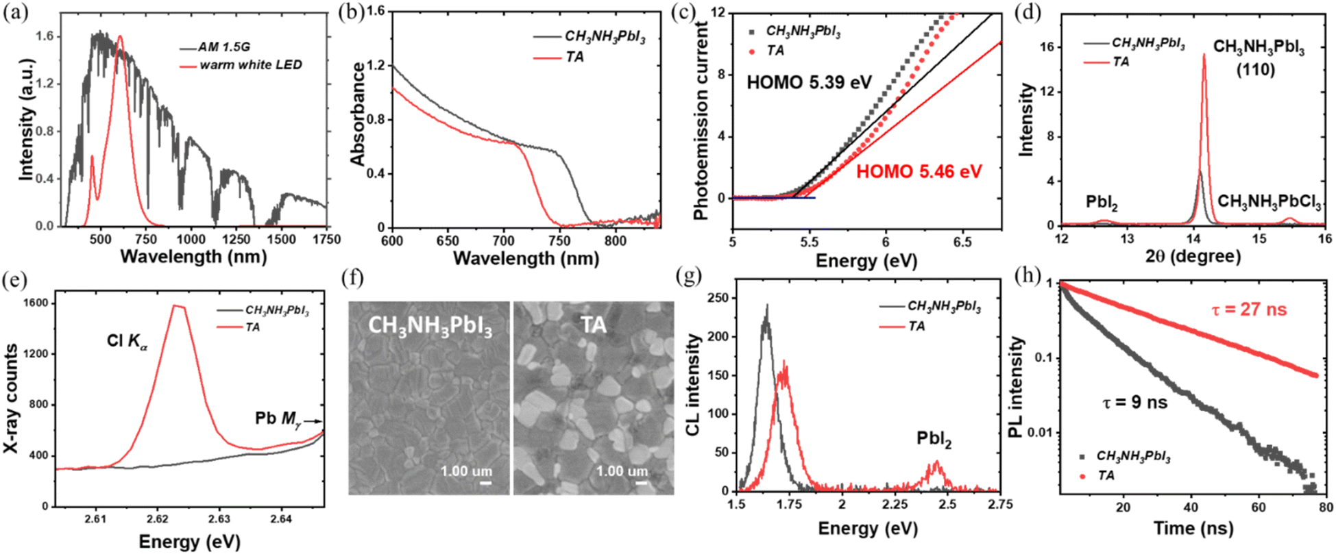 | ||
| Fig. 1 (a) Comparison of the 1 sun spectrum with the warm white LED indoor light source used in this study. (b) Absorbance spectra of triple anion (TA) perovskite film and CH3NH3PbI3 control film from UV-Vis spectroscopy. (c) Ambient photoemission spectra of TA and CH3NH3PbI3 films. (d) X-ray diffraction pattern of TA and CH3NH3PbI3 films (e) wavelength-dispersive X-ray spectra of TA and CH3NH3PbI3 films in the region of the Cl Kα X-ray line showing incorporation of Cl in the TA film. (f) Scanning electron microscopy images of TA and CH3NH3PbI3 films. (g) Room temperature cathodoluminescence (CL) spectra of TA and CH3NH3PbI3 films showing the blue-shifted near band edge emission from the TA films and the appearance of PbI2-related emission. (h) Time-resolved photoluminescence spectra of TA and CH3NH3PbI3 films. Excitation was at 515 nm. | ||
The commonly used approach to widen the bandgap is to adjust the valence band-edge by compositional tuning of the halide ions. Following this approach, iodide-bromide alloying has successfully shifted the bandgap of methylammonium lead iodide (CH3NH3PbI3) from 1.6 to 1.75 eV with a 40% Br ratio.11 However, it is reported that a larger amount of Br incorporation (greater than 20% halide mole fraction) into CH3NH3PbI3 results in phase segregation under illumination or during ageing, making the bandgap shift ineffective and reducing the VOC.12 Suhas et al. have reported that the voltage loss in bromide-iodide wide-bandgap perovskite is not due to halide phase segregation but due to trap density.13 They reported that the accumulated trapped charges act as the driving force for halide segregation. Previous studies have demonstrated the beneficial role of Cl in defect passivation and trap density reduction.14–17 Hence, the addition of Cl to obtain the triple anion (TA) composition is reported as an effective method to suppress phase segregation by modifying the morphology and surface passivation and to realize efficient bandgap tuning.18,19 Starting with FAPbI3 (where FA is formamidinium) to achieve the same wide bandgap would require a larger amount of PbBr2 and PbCl2 which in turn would lead to an undesirable increase in the phase segregation. Also, the photoactive perovskite black phase (α-phase) of FAPbI3 is thermodynamically unstable, and hence it undergoes a spontaneous transformation into the photoinactive δ-phase at room temperature and ambient conditions. The larger ionic radius of FA+ (0.253 nm) and smaller ionic radii of Br− (0.196 nm) and Cl− (0.181 nm) will increase Goldschmidt's tolerance factor above 1 to further increase the phase instability issues and non-ideal perovskite film quality.20 Previously the authors have reported CsPbBr2I-based perovskite composition for indoor photovoltaics.21 CsPbBr2I also suffers phase instability under ambient air conditions (due to a lower tolerance factor of ∼0.8) and yielded a steady state PCE of only about 9% under indoor lighting. The mixed cation (FA/Cs and FA/Cs/MA) perovskite compositions mostly require 30–60 minutes of thermal annealing and can cause the escape of Cl from the perovskite composition unless complex fabrication procedures as reported by Xu et al.18 are followed which in turn can lead to issues with the reproducibility of perovskite active layer preparation and properties.22–24
The wide bandgap TA perovskites have been successfully used in perovskite-silicon tandem solar cells.18 Their suitability for indoor photovoltaic applications has previously been demonstrated in two reports with PCEs of ∼20% and 36%. In both of these reports, the triple anion perovskite layer was prepared using a two-step processing method which increases the complexity of device fabrication, and the thermal annealing times were 15 & 20 minutes. The report with the higher efficiency of 36% used a processing temperature of 250 °C for its PV device fabrication which is not compatible with commonly used flexible substrates such as PET [Table 1]. Though the above results are commendable, the influential role of Cl in the perovskite active layer for efficient indoor light harvesting and the importance of the processing time window to ensure the retention of Cl in the final perovskite film are not yet clear. Given the impetus on the perovskite indoor PV due to the rapidly expanding IoT, it is important to identify perovskite active layer compositions with consistent performance under indoor lighting and develop research methodologies specifically for perovskite indoor PVs.
| Absorber | Device structure | Spin-coating method | Thermal annealing condition (perovskite) | 1-sun forward PCE (%) | 1-sun reverse PCE (%) | Indoor light source (μW cm−2) | Indoor forward PCE (%) | Indoor reverse PCE (%) | Indoor steady-state PCE (%) | Ref |
|---|---|---|---|---|---|---|---|---|---|---|
| MAPbI2−xBrClx | p–i–n | Two steps | 100°C, 15 min (250 °C for NiO HTL) | No data given | 14.6 | 275.4 | No data given | 36.1 | No data given | Cheng et al.9 |
| (FAI)x(MABr)y((Pb(I0.98Br0.02)2)1−z(PbCl2)z) | n–i–p | Two steps | 150 °C, 20 min | No data given | 18.8 | 280 | No data given | 19.2 | No data given | Kim et al.30 |
| MAPbI2.6Br0.2Cl0.2 | n–i–p | One step | 100 °C, 3 min | 14.6 | 16.5 | 300 | 26.1 | 33.6 | 25.1 | This work |
In the present work, we report a facile and fast (3 minutes of processing time at 100 °C) single-step fabrication of TA halide perovskite composition of CH3NH3PbI2.6Br0.2Cl0.2 with a tailored bandgap of 1.69 eV and investigate its indoor light harvesting properties. This composition was selected to reap both the benefits of a widened bandgap (under indoor lighting) but avoid phase segregation and obtain a stable perovskite composition with the additional benefit of passivating traps by adding Cl. MAPbI3 is taken as the control sample, as it is the most widely investigated halide perovskite composition for photovoltaic applications and hence starting with the MAPbI3 benefits the understanding of microstructural evolution and device properties due to the alloying of three halides. The I–Br double halide is not considered in the present study due to its lower stability, severe phase segregation and inferior indoor photovoltaic performance compared to Cl-containing mixed halides or I-single anion (MAPbI3) composition as previously reported.9,19,25–27 The MA volatility and decomposition of MAPbI3 at high temperatures (e.g., >85 °C) impeding the long-term operation/stability has been previously reported.28 However, the TA (MAPbI2.6Br0.2Cl0.2) devices detailed in our manuscript are mainly optimised for their usage inside the buildings (and under indoor lighting) where conditions are much milder compared to 1-sun illumination and such high temperatures do not exist in normal living conditions. Moreover, the volatility of MA ion is of little concern with a well-encapsulated photovoltaic device as this decomposition is highly reversible and self-healing, as reported by Cerratti et al.29 To understand the kinetics of Cl incorporation or escape during the TA perovskite film formation, in situ grazing incidence wide-angle X-ray scattering (GIWAXS) was performed and the presence of Cl was further confirmed through wavelength dispersive X-ray spectroscopy measurements. To gain insight into the benefits of the triple anion alloying method in indoor photovoltaics, we systematically investigated the microstructural, photophysical and optoelectronic properties of CH3NH3PbI2.6Br0.2Cl0.2 films, partial heterostructures and completed devices. Our study revealed that the triple anion composition of CH3NH3PbI2.6Br0.2Cl0.2 suffers significantly fewer defect-related recombination losses, exhibits enhanced charge carrier lifetime, and possesses better crystalline properties in comparison to CH3NH3PbI3 resulting in improved power conversion efficiency and suppressed hysteresis effects under indoor lighting conditions. The decisive role of Cl in the better performance of CH3NH3PbI2.6Br0.2Cl0.2 based indoor photovoltaic devices is further verified by successively reducing the Cl content and correlating it with the corresponding photovoltaic device performance. Table 1 lists the merits and novelty of our work (in terms of overall processing temperature, time and efficiency) compared to the two previously reported triple halide perovskite indoor photovoltaics.
Results and discussion
Microstructural characterization of triple anion perovskite films
To obtain triple anion CH3NH3PbI2.6(BrCl)0.2, equimolar amounts of PbBr2 and PbCl2 were added into the PbI2 stoichiometry-adjusted CH3NH3PbIx precursor solution (with the nominal perovskite composition then assumed to follow that of the precursor stoichiometry). The standard CH3NH3PbI3 perovskite is used as the control sample in the study. During spin coating, both films were washed with anti-solvent diethyl ether followed by a thermal annealing treatment for 3 minutes on a hotplate at 100 °C. A detailed description of the preparation method is given in the experimental section in the supporting information.† The UV-vis spectroscopy measurement was performed initially on TA films and CH3NH3PbI3 control samples to characterize the bandgap properties. As shown in Fig. 1(b) the absorption edge for the TA perovskite composition is blue-shifted from ∼775 nm (CH3NH3PbI3) to 750 nm (TA). This corresponds to an increase in the bandgap from 1.61 eV for CH3NH3PbI3 to 1.69 eV for the TA films (Fig. S1†). The valence band (VB) position was characterized by ambient photoemission spectroscopy (APS) as shown in Fig. 1(c). The TA films showed a VB edge of 5.46 eV, deeper than that of the CH3NH3PbI3 VB at 5.39 eV as expected due to the incorporation of Br− and Cl− anions.To understand the crystalline properties, X-ray diffraction (XRD) characterization was performed (Fig. S2†). Peaks at 14.18° and 28.6° can be indexed to the (110) and (220) diffraction peaks of the tetragonal perovskite phase. For both diffraction peaks, the TA sample shows significantly higher peak intensity indicating its enhanced crystallinity compared to CH3NH3PbI3. Previously Tidhar et al. have shown that the PbCl2 nanoparticles present in the precursor solution can induce the nucleation of the perovskite crystals, by providing heterogeneous nucleation sites for improved perovskite crystallisation.31 The preferential orientation of crystallites in TA films towards (110) direction is suitable for improved charge transport.32
Also, the TA sample revealed the existence of PbI2 with the appearance of a small peak at 12.65°. This observation of PbI2 agrees with the previous research on perovskite compositions containing bromide and chloride anions.18,33Fig. 1(d), shows a typical peak shifting from 14.11° for CH3NH3PbI3 to 14.20° for the TA sample as expected due to shrinkage of the perovskite lattice due to the incorporation of Cl− (1.81 Å) and Br− (1.96 Å) with smaller ionic radii compared to I− (2.20 Å).9 In addition, a new peak is observed at 15.49°, which is considered to be a characteristic peak of CH3NH3PbCl3 as per previous reports.18,33,34 The main challenge with the triple anion alloying compared to the iodide-bromide double halide system is to confirm the presence of Cl in the perovskite lattice because it can volatilize during the thermal annealing process as CH3NH3Cl.17 The existence of the CH3NH3PbCl3 peak provides primary proof that Cl is incorporated and remains within the perovskite active layer instead of volatilizing. Previous research has pointed out the difficulty in detecting chlorine within the perovskite layer after the thermal annealing process although it was present in the precursor solution.35 In the present study, the existence of chlorine in the CH3NH3PbI2.6Br0.2Cl0.2 films was further confirmed using wavelength dispersive X-ray (WDX) spectroscopy. By contrasting the WDX results from the CH3NH3PbI3 and TA samples respectively, it is evident that Cl is incorporated within the TA samples. Fig. 1(e) compares the WDX counts from the Cl content of CH3NH3PbI3 and TA samples; the CH3NH3PbI3 sample has a bremsstrahlung (continuum) background of ∼300 counts, while the TA sample shows a clear characteristic X-ray peak (∼1600 counts) at the Cl Kα energy, confirming the presence of Cl within the perovskite active layer. Monitoring the WDX peak count rates over 10 minutes verified that there was minimal dissociation/volatilisation caused by the incident 8 keV electron beam [Fig. S3(a–c)†]. This precaution was taken based on the previous studies, where it has been shown that under the high dose electron beam, methylamine and hydrogen iodide (hydrogen halide) can escape from the halide perovskite samples due to electron beam induced damage.36–38Fig. 1(f) show the SEM images of CH3NH3PbI3 and TA thin film samples. For both films, the surface morphology was compact and dense whereas, in the case of the TA sample, dark and bright contrast domains were observed. According to previous research, the brighter domains may be PbI2.39 Although the XRD spectra of the TA samples indicated the presence of PbI2, its presence has been further verified using low electron beam voltage (and hence surface-sensitive) cathodoluminescence (CL) spectroscopy. As shown in Fig. 1(g), the CL emission spectrum of the TA sample shows two emission peaks; one corresponds to its near band-edge emission and the other at ∼2.5 eV arising from the PbI2.39 Also, the near band-edge CL emission of the TA sample is blue-shifted compared to the control CH3NH3PbI3 sample as expected. The peak of the near band-edge CL emission energy from both the CH3NH3PbI3 (1.63 eV) and TA (1.73 eV) sample is found to be slightly higher than the band gap energy estimated using the UV-vis absorption spectra. This could be due to the bandgap energy estimated from the absorption edge being lower than the actual bandgap due to the existence of tail states in the CH3NH3PbI3 and TA films.40 Also, the UV-vis absorption measurements probe the full thickness (350 nm) of the sample, whereas the CL analysis depth is limited by the beam energy; with the 5 keV electron beam used, the penetration depth and hence the signal generation depth is estimated as ≈240 nm using a Monte–Carlo simulation method.41 This would mean that any vertical compositional heterogeneity, as the authors have previously noted in all-inorganic mixed halide perovskites,42 can also contribute to this slightly higher CL emission energy compared to the band gap energy estimated from the UV-vis measurements.
The measured time-resolved photoluminescence (TRPL) data shown in Fig. 1(h) clearly show a much slower decay for TA films than for CH3NH3PbI3 films. The fitted decay time τ is 27 ns for TA films and 9 ns for CH3NH3PbI3 control films, indicating fewer trap states and non-radiative recombination losses for triple anion films. The PbI2 induced by the triple anion alloying method and the incorporated Cl has been reported to effectively passivate the defects in the perovskite layer and reduce non-radiative recombination, which will be further discussed in the photovoltaic properties section.39,43–45 Theoretical studies have shown that Cl incorporation reduces the lattice constant (lattice volume) [which agrees with the XRD analysis of the TA films as shown in Fig. 1(d)] and significantly increases the formation energy of the interstitial defects, thus helping to reduce the trap states.46 Also, the perovskites grown under I-rich conditions have a high density of trap states, due to the low formation energy of Pb–I antisite deep traps. When PbI2 in CH3NH3PbI3 is partly replaced by PbCl2 and PbBr2, in TA films, excess iodine is reduced and can thus lower the trap density as confirmed by the enhanced carrier lifetime of the TA films from the TRPL measurements.47 After confirming the wider bandgap, better crystalline quality, compact surface morphology, enhanced PL lifetime and the presence of Cl in the CH3NH3PbI2.6Br0.2Cl0.2 films, the photovoltaic properties of the TA films were characterized and compared to those of CH3NH3PbI3.
Photovoltaic properties
To investigate the photovoltaic device performance of the TA perovskites, devices were fabricated in typical n–i–p planar architecture with a layer structure of glass/ITO/SnO2/perovskite/Spiro-OMeTAD/Au. The J–V scan measurements were performed for the CH3NH3PbI3 and TA devices under indoor warm white LED illumination of 1000 lux (0.3 mW cm−2) and 1 sun. The J–V characteristics and the PCE distribution from these measurements are shown in Fig. 2. The corresponding photovoltaic performance parameters are shown in Fig. S4, Tables 2 and S1.† The box plots in Fig. 2 and S4† present the distribution and average PCE of more than 20 photovoltaic devices and the performance parameters of VOC, FF and JSC. The J–V characteristics of the champion devices under indoor illumination are given in Fig. 2(a). The TA device shows a maximum PCE of 26.1% for the forward scan and 33.6% for the reverse scan. The CH3NH3PbI3 control devices present a forward scan PCE of 21.0% and reverse scan PCE of 30.1% for their best performance. As shown in the box plots in Fig. 2(b) and Table 2, the average PCE of TA devices reaches 22.6% for the forward scan and 30.1% for the reverse scan while for CH3NH3PbI3 devices it is only 17.8% and 27.8% respectively, which shows a substantial enhancement of indoor light harvesting by the TA films. From Fig. 2(a) and (c), and Table 2 it can be seen that a significant part of the enhancement in PCE of the TA device under indoor lighting is due to the higher VOC which is 0.86 V and 0.89 V for different scan directions. The corresponding VOC for the CH3NH3PbI3 control sample is only 0.78 V and 0.84 V, respectively. The fill factor of TA devices is also consistently improved particularly for the forward scan: the average FF of TA devices is 57.2% while that of CH3NH3PbI3 devices is only 46.5%. The significant improvement of FF indicates better charge extraction and collection in the TA films and can be attributed to the better crystalline quality, better charge transport, low trap density and enhanced carrier lifetime of TA films compared to CH3NH3PbI3. On the other hand, the JSC of both types of devices are comparable under indoor illumination as shown in Fig. S4(c)† and Table 2 (forward scan: 0.15 mA cm−2 for CH3NH3PbI3vs. 0.14 mA cm−2 for TA; reverse scan: 0.14 mA cm−2 for CH3NH3PbI3vs. 0.13 mA cm−2 for TA). Fig. 2(f) shows the external quantum efficiency (EQE) spectra. The blue shift of the TA absorption edge, compared to CH3NH3PbI3 is evident and supports the UV-vis absorption measurements. Fig. 2(f) also shows the emission spectrum of the indoor warm white LED source used in the present study.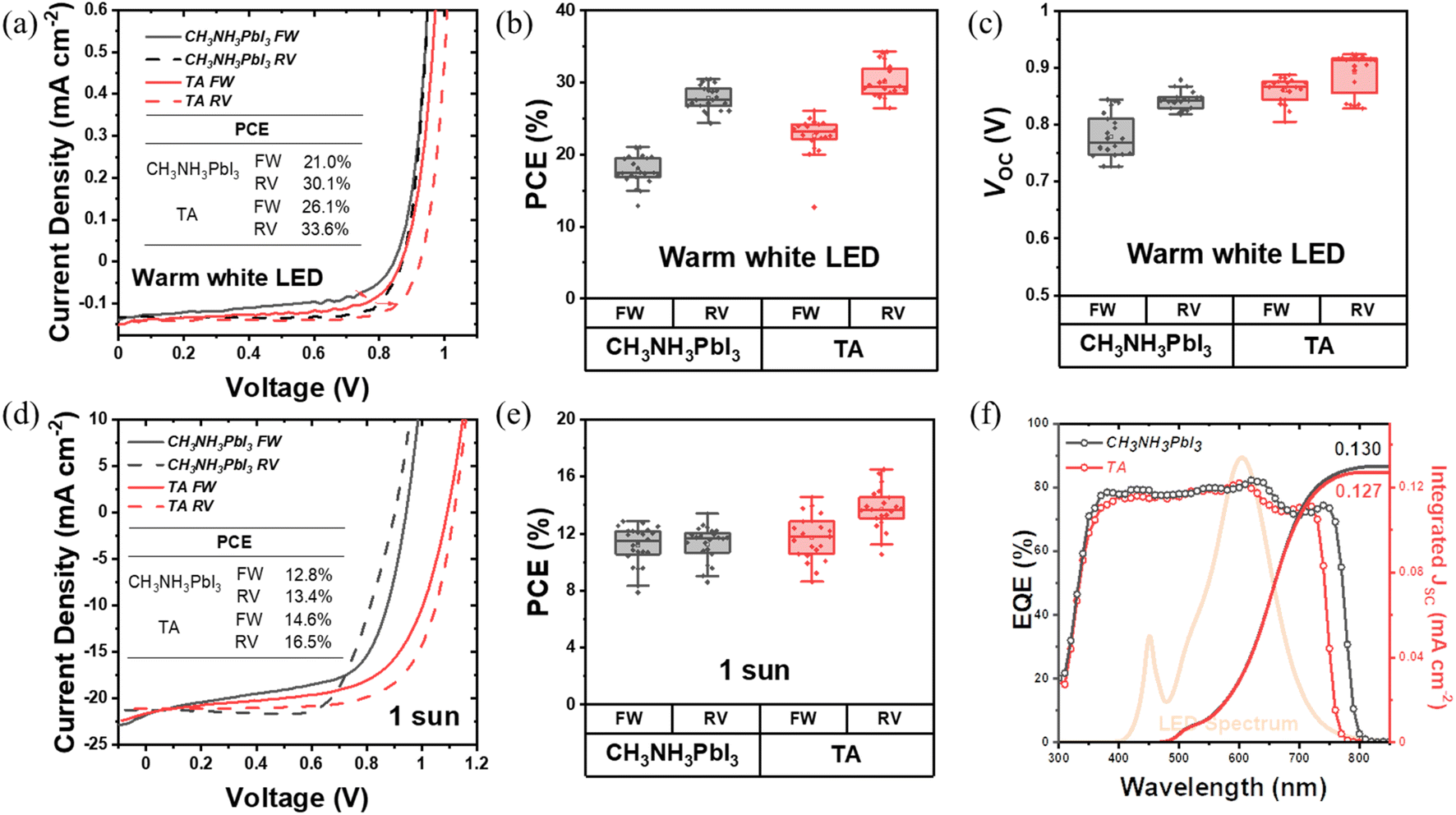 | ||
| Fig. 2 (a) J–V curves of TA and CH3NH3PbI3 based devices under warm white LED illumination. (b) The statistical distribution of PCE values of TA and CH3NH3PbI3 devices under warm white LED illumination. (c) The distribution of VOC of two types of photovoltaic devices under warm white LED illumination. (d) J–V curves of TA and CH3NH3PbI3 under 1 sun illumination. (e) The statistical distribution of PCE values of TA and CH3NH3PbI3 devices under 1 sun illumination. (f) EQE spectra and integrated JSC under warm white LED illumination for the TA and CH3NH3PbI3 devices. The irradiance spectrum of the warm white LED illumination used in the present study is also shown. | ||
| Device type | Average PCE (%) | Average FF (%) | Average JSC (mA cm−2) | Integrated JSC from EQE (mA cm−2) | Average VOC (V) | |
|---|---|---|---|---|---|---|
| CH3NH3PbI3 | FW | 17.8 ± 2.0 | 46.5 ± 4.1 | 0.147 ± 0.004 | 0.130 | 0.779 ± 0.039 |
| RV | 27.8 ± 1.7 | 75.4 ± 3.7 | 0.131 ± 0.004 | 0.844 ± 0.017 | ||
| TA | FW | 22.6 ± 2.8 | 57.2 ± 5.6 | 0.138 ± 0.009 | 0.127 | 0.860 ± 0.022 |
| RV | 30.1 ± 2.3 | 78.4 ± 5.0 | 0.129 ± 0.007 | 0.892 ± 0.036 |
As for the device performance under 1 sun, from the J–V curves in Fig. 2(d), TA devices reach a maximum PCE of 14.6% for forward scan, and 16.5% for reverse scan, while the PCE of the CH3NH3PbI3 control device is only 12.8% for the forward scan and 13.4% for the reverse scan for its champion device. From Fig. 2(e), it is noticed that the overall PCE of TA devices is slightly improved compared to CH3NH3PbI3 under 1 sun. A comparison of the photovoltaic performance parameters in Fig. S4(d)† shows that the average VOC of TA devices is improved to 1.06 V compared to that of 0.9 V for CH3NH3PbI3. This observation of higher VOC for TA devices is consistent with their larger bandgap compared to CH3NH3PbI3, as revealed by UV-vis spectroscopy and APS measurements [Fig. 1(b) and (c)].
The JSC from both types of devices are broadly comparable (forward scan: 19.0 mA cm−2 for TA vs. 19.2 mA cm−2 for CH3NH3PbI3; reverse scan: 17.9 mA cm−2 for TA vs. 18.0 mA cm−2 for CH3NH3PbI3 from Fig. S4(f) and Table S1†). The fill factors of these devices are also within a similar range, being 61.3% and 56.9% for forward, and 70.1% and 71.6% for reverse scans for CH3NH3PbI3 and TA devices, respectively. These results show that the triple anion alloying method is effective in boosting the VOC without compromising JSC and FF thus yielding higher PCE.
The PCE obtained from the maximum power point tracking (MPPT) measurements is shown in Fig. 3(a). Under 1000 lux warm white LED illumination, the steady-state PCE of TA device reaches as high as 25.1%, which is significantly higher than 17.9% for CH3NH3PbI3 devices. Thus under 1000 lux illuminance conditions, the TA devices can deliver a steady-state power output of 75.4 μW cm−2 compared to the 53.7 μW cm−2 from the CH3NH3PbI3 devices. These results are summarized in Table 3. Regarding the current IoT wireless protocols industry, the 75.4 μW cm−2 power density would allow a 20 cm2 TA perovskite indoor photovoltaic device to power most of the RFID, LoTA Backscatter, Passive Wi-Fi, BLE, ANT and ZigBee nodes.2 The excellent steady-state PCE of the TA device further proves the superiority of the triple anion alloying method.
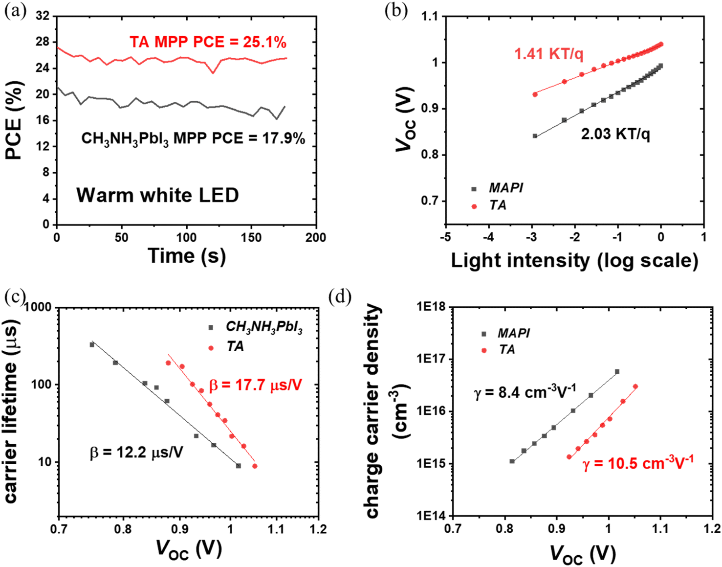 | ||
| Fig. 3 (a) MPPT PCE comparison of TA and CH3NH3PbI3 devices under warm white LED illumination. (b) VOC variation versus light intensity. (c) Transient photovoltage characterization of TA and CH3NH3PbI3 devices. (d) Transient photocurrent characterization of TA and CH3NH3PbI3 devices. | ||
| Light source | Device type | Steady state PCE (%) | Output power density (μW cm−2) |
|---|---|---|---|
| Warm white LED (1000 lux) | CH3NH3PbI3 | 17.9 | 53.7 |
| TA | 25.1 | 75.4 |
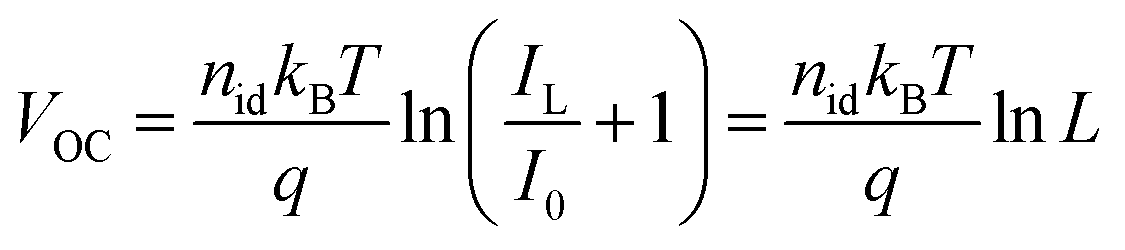
To gain more insight into the enhanced photovoltaic properties of TA devices, light intensity-dependent J–V characterization, transient photocurrent (TPC) and photovoltage (TPV) measurements were carried out. Under low-intensity indoor lighting conditions, suppression of trap states is crucial to maximize the power output and therefore non-radiative recombination losses were studied by plotting VOCvs. light intensity (L).48 The relationship between L and VOC is given as:49
 | (1) |
In general, an ideality factor of 1 (or close to 1) indicates the dominant recombination mechanism is bimolecular (radiative) recombination, whereas values closer to 2 indicate pronounced trap-assisted Shockley–Read–Hall (SRH) recombination.50,51 From Fig. 3(b), the ideality factor calculated for CH3NH3PbI3 is 2.03, while for TA it is only 1.41, indicating that the non-radiative recombination is significantly reduced for the TA devices, which is consistent with the TRPL measurement shown in Fig. 1(h). In addition to TRPL characterization of TA and CH3NH3PbI3 films on bare ITO substrates, TRPL was also carried out for perovskite films deposited on SnO2/ITO films (SnO2 is the ETL in the device architecture considered here). By taking the TRPL ratio of perovskite films on electron transport layer SnO2 to the perovskite films on bare ITO substrate, we account for the natural PL decay in perovskite films and get the decay which is caused solely by electron extraction. The PL ratio shows a very similar decay time of ∼40 ns for both perovskites which indicates that the electron extraction rate is the same for CH3NH3PbI3 and TA (Fig. S5†).52 Hence, the longer lifetime of free carriers from the TA perovskite film provides more efficient charge extraction which significantly enhances FF. TPV and TPC measurements were used to further investigate the improvements in carrier lifetime. Fig. 3(c) shows carrier lifetime variation as a function of VOC (light intensity). The steep decrease in carrier lifetime at higher VOC is attributed to faster carrier recombination owing to higher light intensity. The results in Fig. 3(c) reveal that the carrier lifetime of TA devices is consistently higher than that of CH3NH3PbI3 devices, supporting their improved photovoltaic performance as shown in Fig. 2, and implying their reduced trap states and better interface conditions. The equation of carrier lifetime versus VOC used to extract β is given below (extracted from TPV measurements):53
τ = τ0![[thin space (1/6-em)]](https://www.rsc.org/images/entities/char_2009.gif) e−βVOC e−βVOC | (2) |
| n = n0eγVOC | (3) |
TA devices exhibit a higher γ parameter (10.5 cm−3 V−1) for the rate of increase of charge density n compared to that of CH3NH3PbI3 (8.4 cm−3 V−1). The γ parameter is the rate of increase of n with respect to bias which has a value of 19 V−1 for an ideal semiconductor (γ ≈ e/2kBT).53 The larger deviation from ideality of the γ parameter of the CH3NH3PbI3 device indicates more non-radiative recombination, suggesting a higher density trap state for CH3NH3PbI3 devices compared to TA devices, and agrees with the findings of VOCvs. light intensity measurements. The higher γ parameter of TA devices implies better interfacial conditions (as previously reported for Cl containing mixed halide perovskites32) which also agrees with the improved decay lifetime τ from the TRPL measurements. The perturbed lifetime τΔn can be related to the total charge density with a power dependence in η through the following equation:53
 | (4) |
The exponent η can be obtained by fitting τΔnvs. the charge density n; it can also be obtained by rearranging eqn (2) and (3) (η = β/γ). η for TA and CH3NH3PbI3 devices is 1.68 and 1.44, respectively. The η exponent can be used to calculate the total lifetime for devices from the perturbed lifetime using eqn (5). With the higher η value, the calculated total lifetime will be higher for TA devices with higher intrinsic perturbed lifetime, which further confirms reduced trap states from triple anion perovskites.
| τn = (η + 1)τΔn | (5) |
The reduced non-radiative recombination, prolonged lifetime and better interfacial properties can be linked to improved device performance and emphasize the importance of controlling traps for maximizing the efficiency of indoor photovoltaic devices. These enhanced optoelectronic properties of TA devices can be mainly attributed to two aspects as revealed through microstructural characterizations. Firstly, the chlorine doping enhanced perovskite crystallinity and reduced trap states by coordinating the triple halide system and passivation.17,30,43 Secondly, the PbI2 induced by the triple anion alloying method plays a synergetic role in the system. Moderate PbI2 induced at interfaces can passivate the interfacial defects, suppressing the non-radiative recombination losses. With a type 1 band alignment at the perovskite/HTL interface, moderate amounts of PbI2 can diminish the barrier for hole extraction and improves the charge selectivity by changing the grain boundary bending from downward to upward, which reduces the recombination between the electrons from the perovskite active layer and holes from HTL.54
Role of Cl in the enhanced photovoltaic properties of TA devices
To obtain deeper insight into the better indoor photovoltaic properties of the TA composition, the influence of the halide content needs to be investigated. Since bromine is relatively stable, it is particularly important to investigate how the indoor photovoltaic device properties are influenced by chlorine content. Previously, the thermal annealing process has been successfully used to vary the Cl content in a double halide CH3NH3PbI3−xClx perovskite layer.33 This was made possible because of the volatile nature of Cl, allowing the incorporated chlorine to be released in the form of CH3NH3Cl during thermal annealing.31 In the present investigation, we used a similar thermal annealing method to control the content of chlorine in the TA perovskite layer. We selected the thermal annealing of 1 minute vacuum annealing, followed by 2 min, 10 min, 30 min, 45 min and 60 min with the same temperature 100 °C to investigate the effect of chlorine content. We used WDX spectroscopy to estimate the Cl content in the resultant TA perovskite layers. The iodine and bromine contents are relatively stable during the different duration of the thermal annealing process as shown in Fig. S6.†Fig. 4(a) shows WDX spectra in the region of the chlorine Kα characteristic X-ray line, after background correcting by subtracting the corresponding spectrum for Cl-free CH3NH3PbI3. This background correction accurately accounts for both the bremsstrahlung continuum radiation and the tail of the nearby Pb Mγ line at 2.653 keV (see Fig. 1(e)). The resultant net X-ray peak intensity shows the trend of chlorine content decline on increasing the annealing duration. The 2 min-annealed sample has the highest chlorine content with a peak of over 1200 X-ray counts, reducing to a near-negligible signal after 60 min annealing. In the absence of readily available WDX standards of a suitably close composition, it is adequate for the purposes of this work to estimate relative compositions based on the assumptions that (i) the 2 minute annealed TA sample is close to its nominal CH3NH3PbI2.6Br0.2Cl0.2 stoichiometry, and (ii) any atomic number, X-ray absorption and secondary fluorescence (“ZAF”) effects are minimal. The estimated Cl wt% is thus 1.2%, 0.74%, 0.13%, 0.03% and 0.003% respectively for the 2, 10, 30, 45 and 60 minute annealed TA samples. This WDX result matches the results from the Sun et al. study, which constructs a Cl content gradient to investigate the effect of chlorine.33 It is noteworthy that, except for the 2 minute thermally annealed sample, the Cl content in different TA samples is relatively stable with respect to the WDX electron beam irradiation duration of 10 minutes, as shown in Fig. S6(f).† While some slight reduction in counts is seen in the Cl peak intensity (strongest, as expected, in the 2 minutes thermally annealed TA sample which retains the most Cl), the magnitude is not sufficient to have a significant effect on the measured WDX compositions.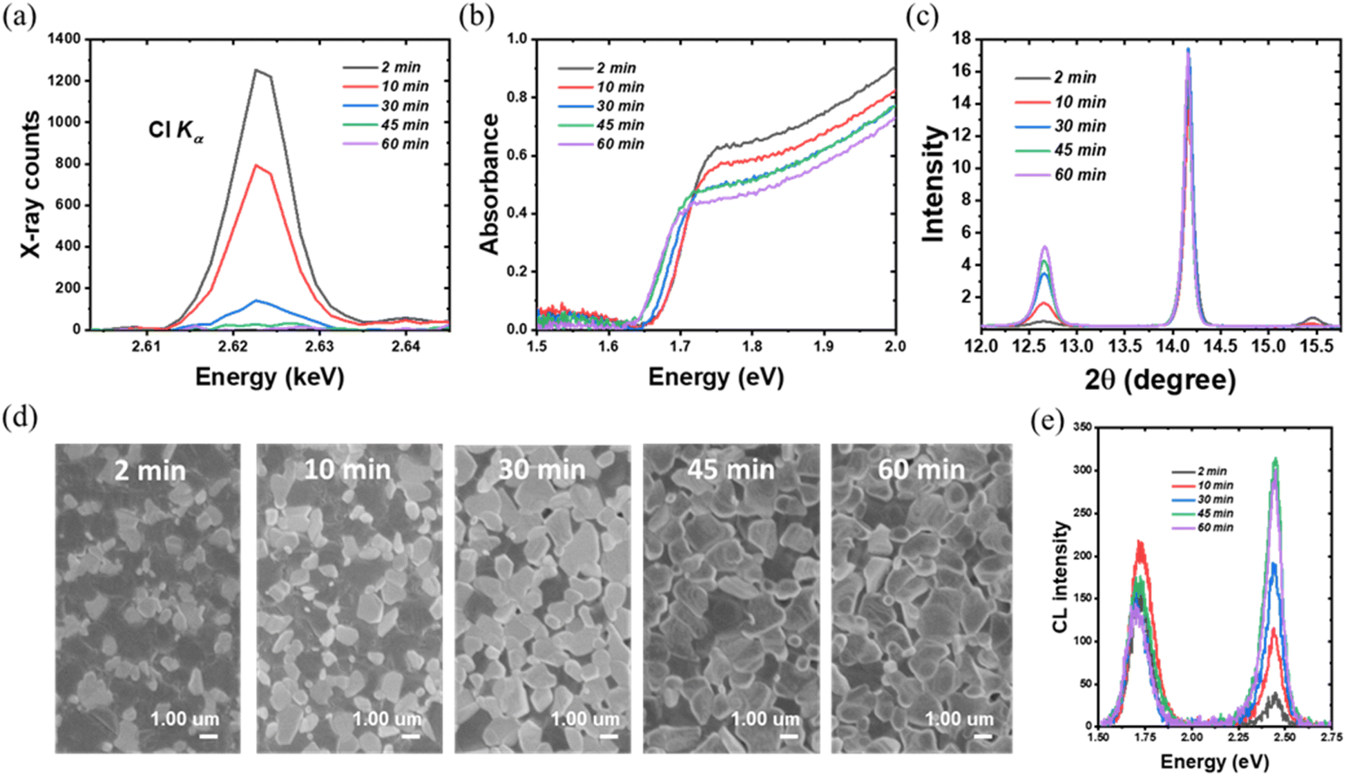 | ||
| Fig. 4 (a) Background-corrected wavelength dispersive X-ray spectra of the Cl Kα line as a function of thermal annealing time. (b) Absorbance spectra of triple anion incorporated perovskite film based on different thermal annealing times. (c) X-ray diffraction pattern showing the effect of thermal annealing of the TA films. (d) Secondary electron (SE) images of annealed films as a function of different thermal annealing duration. The contrast domains represent PbI2. (e) Cathodoluminescence spectra of TA films showing the enhanced CL emission with the increase in thermal annealing duration. | ||
Fig. 4(b) shows the UV-vis absorption spectra of the TA films with different Cl content, revealing a redshift with the decreasing chlorine content. The absorption edge of the 2 min annealed sample is at ∼1.69 eV and is gradually shifted to ∼1.64 eV for the 60 min annealed sample, in which the chlorine content is negligibly small. The redshift in the absorption edge with a longer annealing time is consistent with the WDX characterization that chlorine is constantly reduced in the thermal annealing process. The crystalline properties of the TA perovskite layer as a function of thermal annealing (and hence as a function of chlorine content) were investigated by XRD. The peaks at 14.18° and 28.6° which index to (110) and (220) planes of the tetragonal perovskite phase remain. Another significant change can be noticed from the CH3NH3PbCl3 characteristic peak at 15.49°. Though the CH3NH3PbCl3 peak can be identified from the 2 min-annealed samples (with the highest chlorine content as per the WDX data), it is then reduced dramatically in the 10 min-annealed samples and completely disappeared in other samples, which further implies the escape of chlorine during the thermal annealing process. In addition, along with decreasing chlorine, the intensity of the PbI2 characteristic peak at 12.65° is enhanced as the thermal annealing time increases.
Fig. 4(d) shows the secondary electron SEM images of the TA films as a function of different thermal annealing duration. From Fig. 4(d), with longer thermal annealing time, the density of white domain-like features most likely related to the PbI2 phase is increased, which is consistent with the XRD results. For the 45 min and 60 min annealed samples, which only have a trace amount of chlorine, the PbI2 features dominate the film surface. The increased PbI2 further matches the CL emission results shown in Fig. 4(e). Besides the TA perovskite near band-edge emission peak, the PbI2 peak at 2.4 eV is significantly enhanced for samples annealed for 45 and 60 minutes.
The removal of the chlorine content from the TA samples is further verified using in situ and static grazing incidence wide-angle X-ray scattering (GIWAXS) experiments. From Fig. 5(a)–(e), the GIWAXS diffraction peaks located at q ∼1.0 and ∼2.0 Å−1 correspond to the (110) and (220) lattice planes, in line with the XRD peaks at 14.18° and 28.6° (ref. 55 and 56) as shown in Fig. S2.† The PbI2 diffraction peak at q ∼0.9 Å−1 appears with arc-like scattering with preferred out-of-plane orientation.57 The PbI2 peak intensity increases with the longer annealing time as evidenced by the XRD peaks at 12.65°. Notably, the CH3NH3PbCl3 crystals exhibit preferred out-of-plane orientation for the 2 min and 10 min annealed TA films, as evidenced by the peak at q ∼1.1 Å−1, which further emphasizes the presence of chlorine within the TA samples. Consistent with the XRD and WDX results, the 2 min annealed films have the strongest diffraction intensity (at q ∼1.1 Å−1) corresponding to CH3NH3PbCl3 crystals. The CH3NH3PbCl3 phase then gradually decreases and vanishes completely for 30 minutes and longer thermally annealed samples. To probe the evolution of phases during thermal annealing, in situ GIWAX measurements were performed based on prepared 2 minute annealed TA perovskite films as a function of thermal annealing time as shown in Fig. 5(f). The PbI2 gradually increases with a longer annealing process while the CH3NH3PbCl3 phase gradually decreases and vanishes at around ∼100 seconds of the 100 °C thermal annealing process.
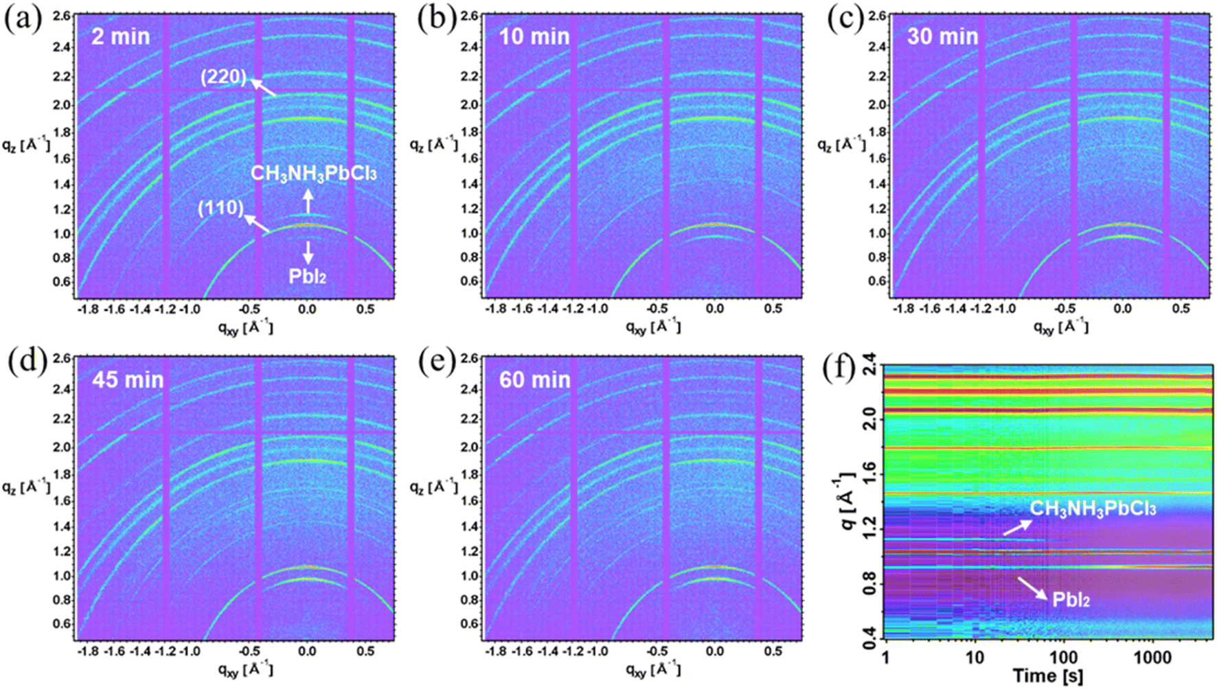 | ||
| Fig. 5 (a)–(e) Grazing incidence wide-angle X-ray scattering diffraction patterns of TA films thermally annealed at 100 °C for different durations. With a longer thermal annealing time, the PbI2 diffraction peaks increase whereas the CH3NH3PbCl3 diffraction peaks decrease (f) False-colour plot of in situ GIWAXS pattern during the thermal annealing process for the pre-prepared 3 min-annealed TA film. | ||
The evolution of the q position of the TA perovskite (110) peak during thermal annealing can give information about the changes in the composition of the TA perovskite phase (i.e. incorporation or removal of Cl), as shown in Fig. S7.† During the initial ramping of temperature from 25 °C to 100 °C, a change in the q position to lower values (increase in (110) d-spacing) can be attributed to lattice expansion dominated by thermal expansion. The subsequent changes in q position occur at a constant temperature (100 °C) and hence can be attributed to changes in the composition of the TA perovskite phase. Upon reaching 100 °C, the evolution of the q position indicates a shrinkage of the lattice constant for the initial 5 min of annealing followed by an expansion of the lattice constant for a longer annealing time. We recall that the CH3NH3PbCl3 phase dissociates during the initial annealing time giving rise to the release of Cl ions that can be incorporated into the TA perovskite phase. Therefore, we hypothesize that the initial shrinkage of the lattice constant of the TA perovskite phase results from the incorporation of smaller ions (such as Cl) into the TA perovskite phase. These Cl ions are perhaps supplied from CH3NH3PbCl3 phase dissociation. However, for longer annealing times, some of these Cl leave the film due to the high volatility of Cl, in agreement with previous studies. These results reveal that careful optimization of annealing time can be used to control the Cl content in TA perovskite films.
The indoor photovoltaic properties of the devices with different thermal annealing times are characterized to investigate the effect of chlorine release and PbI2 growth. In terms of Fig. 6, S8 and Table S2,† the optimized annealing time is 2 minutes, with these devices reaching the highest PCE of 26.6% and 30.1% for forward and reverse bias, respectively. The lowest PCE is obtained from 30 min-annealed devices (forward: 18.4%; reverse: 26.8%), followed by 60 min-annealed devices (forward: 19.0%; reverse: 28.9%). Regarding the variation of photovoltaic parameters, 2 min-annealed samples hold the highest VOC of 0.87 V and 0.92 V among the five conditions, with VOC continuously decreasing during the annealing process. Notably, 2 min-annealed devices gave the highest FF of 57.2% and 78.4%. This drop in FF with longer annealing suggests the worsening of interface conditions and transport properties. The 2 min-annealed TA samples show the highest MPPT PCE as well [Fig. 6(b)]. This observation of degradation in photovoltaic device performance with enhanced thermal annealing time can be attributed to two reasons: (a) the escape of Cl and hence the loss of beneficial effect of Cl in trap reduction/passivation; and (b) the formation of excess PbI2 at the interface of perovskite/HTL. Although moderate amounts of PbI2 can passivate defects and reduce recombination losses, their presence above the threshold limit can deteriorate the device's performance due to the photolysis process. Under illumination, the excess PbI2 can dissociate into Pb(0) [metallic Pb] and I2 gas. This metallic Pb itself can act as a recombination center and the escape of I2 can leave voids in the active layer, blocking the charge collection. With the increase in thermal annealing duration, the presence of PbI2 systematically increased, and this can lead to increased recombination losses as reflected in the continuous decrease of VOC in these devices (Table S2†).39,58
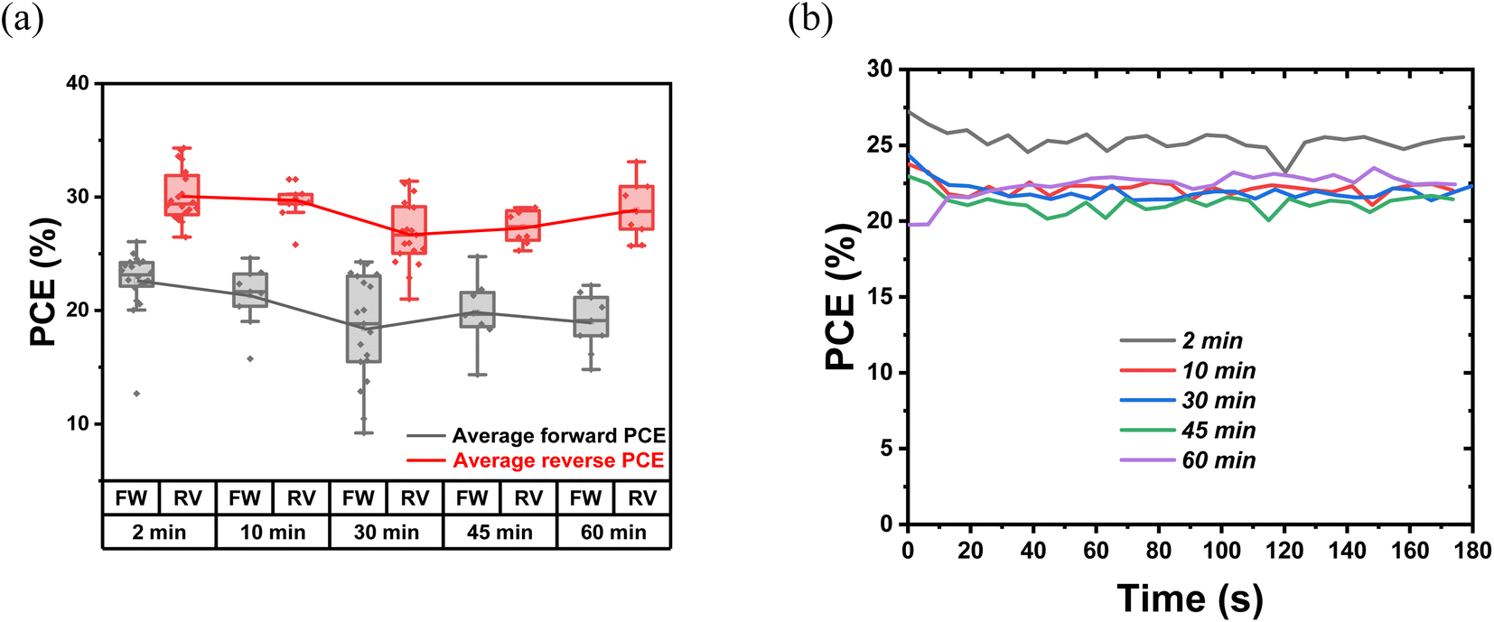 | ||
| Fig. 6 (a) The statistics of PCE of devices as a function of different thermal annealing time under 1000 lux warm white LED illumination. The 2- min-annealed samples hold the highest average PCE of 26.6% and 30.1%. (b) The comparison of MPPT PCE of devices as a function of different thermal annealing time. | ||
Hysteresis properties
Our recent investigation has shown that compared to 1 sun illumination, the halide perovskite photovoltaic devices demonstrate a completely different J–V hysteresis behaviour under indoor lighting conditions, depending on the selection of the device architecture and the photoactive layers.59 Compared to CH3NH3PbI3, TA devices show slightly greater J–V hysteresis under 1 sun illumination, [Fig. 2(e)]. However, under indoor lighting illumination, J–V hysteresis of TA devices is suppressed in comparison to the control CH3NH3PbI3 devices [Fig. 2(b)]. The more pronounced J–V hysteresis of TA devices under 1 sun compared to indoor illumination can be related to the higher possibility of light-induced ion migration effects under 1 sunlight intensity and the presence of different types of halide ions in the TA composition.60–64 Previously we have shown that the SnO2/perovskite interface can contribute to J–V hysteresis in halide perovskite indoor photovoltaic devices.59 However, the origin of the hysteresis effect can also be due to the interfacial defects existing at the perovskite/Spiro-OMeTAD interface.65In this case, we employed P3HT as the hole transport layer to replace Spiro-OMeTAD. Under indoor lighting, the PCE of P3HT-based devices reached 20.4% and 20.6% for forward and reverse bias. Notably, the hysteresis of P3HT-based devices is reduced drastically compared to Spiro-OMeTAD based devices, as shown in Fig. S9,† indicating that the Spiro-OMeTAD interface as well as the SnO2/perovskite interface are contributing to the J–V hysteresis.59 However, the photovoltaic performances of P3HT-based devices are consistently lower than Spiro-OMeTAD devices and one contributing factor could be the low conductivity of the undoped P3HT films used as the HTL.
Powering a temperature sensor
To investigate the reliability of the TA indoor photovoltaic devices as a power source for sensors, a sensor-powering experiment was carried out. Rajan et al. developed a wearable graphene-based textile temperature sensor with a 1 V requirement for operation.66 The graphene-based sensor shows a negative thermal coefficient of resistance, indicating that its intrinsic resistance is reduced with increased temperature. The output voltage from TA devices is tested under two indoor illumination conditions: a) ambient indoor CFL light from the ceiling (220 lux); b) domestic LED table lamp (1000 lux). The obtained output voltages are 1.62 V and 1.86 V, respectively. Fig. 7(a) shows the experimental setup. The Keithley source meter is only used to measure the current across the graphene temperature sensor; no extra voltage from the Keithley source meter is applied. Fig. 7(b) shows the resistance variation of the sensor, powered using TA devices under the two selected indoor illumination conditions. The temperature sensor shows a consistent trend in resistance reduction with an increase in temperature, similar to that previously reported using a Keithley source meter as the voltage source.66 These results indicate that TA perovskite-based indoor photovoltaic devices are reliable for self-powering the low-power sensors. The sensor powering in the real scenario is an important step toward achieving the vision of IoT connection in the real life. In addition to this, the powering reliability is also dependent on the long-term stability of the perovskite photovoltaic device. We have investigated the shelf-life stability of the TA perovskite-based indoor photovoltaic devices by measuring the device on the first day as fabricated, 2 months, 6 months, and 2 years and the results are shown in Fig. S10(a).† These devices were unencapsulated, kept in dark, at ambient conditions inside a dry air desiccator (with a relative humidity of 11%) at room temperature (22 °C). Impressively, these devices either retain their original PCE or show slightly better PCE even after 23 months, suggesting the brilliant long-term stability of TA-based photovoltaic devices. The operational stability of the corresponding devices under continuous indoor lighting illumination (same as in Fig. 2(f)), under ambient air conditions (room temperature 22 °C, relative humidity of 42%) for 12 hours is also shown in Fig. S10(b).† No drop in PCE is observed confirming the excellent ambient operational stability of the TA devices.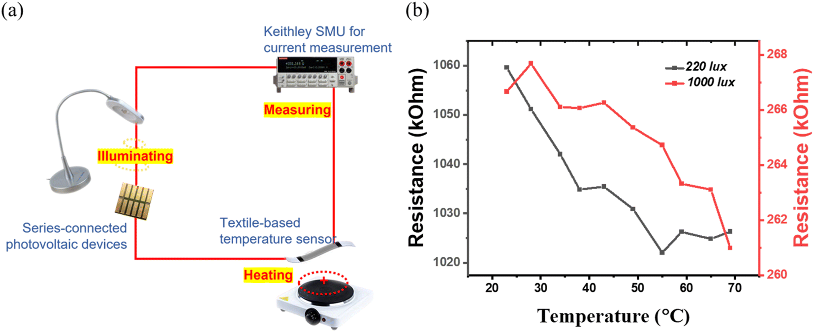 | ||
| Fig. 7 (a) Illustration of sensor powering with TA perovskite indoor photovoltaic device powering a graphene-based textile temperature sensor. (b) Resistance variation of the temperature sensor in two different illumination conditions. | ||
Conclusions
In conclusion, the need for efficient indoor light harvesting was addressed by developing an easily processed, composition-tuned wide bandgap triple anion perovskite CH3NH3PbI2.6(BrCl)0.2. Our study revealed that to keep the Cl in the triple anion perovskite and to reap the beneficial effects of high VOC and enhanced charge carrier lifetime, the thermal annealing duration should be carefully optimized. Detailed microstructural and optoelectronic investigations of the triple anion perovskite revealed its excellent crystalline quality, widened bandgap, lower density of trap states and longer carrier lifetime, all contributing positively to the enhanced photovoltaic properties. The corresponding optimized indoor photovoltaic devices were capable of delivering a steady-state output power of 75.4 μW cm−2 under 1000 lux warm white LED illumination and successfully self-powered a textile integrated graphene based temperature sensor. The study shows the promise of simply processed triple anion perovskites for indoor photovoltaic cells to sustainably power small sensor components in the IoT.Data accessibility
The research data underpinning this publication can be accessed at https://doi.org/10.17630/93ab4fa0-34e3-45a9-aa48-032dec3f675e [REF].†Conflicts of interest
The authors declare no conflict of interest.Acknowledgements
LKJ acknowledges funding from UKRI-FLF through MR/T022094/1. LKJ also acknowledges, Professor Iain Baikie for assistance with the work function and APS measurements, and Professor Phil King and Gordon Kentish, School of Physics and Astronomy, University of St Andrews for the XRD measurements and would like to acknowledge (EPSRC): EP/T023449/1. LKJ wishes to extend her acknowledgement to Professor David Cahen, Weizmann Institute of Science for the many valuable discussion on the Cl incorporation, especially at the revision stage. This research used resources of the Advanced Light Source, a U.S. DOE Office of Science User Facility under contract no. DE-AC02-05CH11231. Work was performed at beamline 12.3.2, beamline scientist Nobumichi Tamura. M. A. acknowledges support by the US Department of Energy, Office of Science, Office of Basic Energy Sciences, Materials Sciences and Engineering Division under Contract No. DE-AC02-05-CH11231 (D2S2 program KCD2S2). Work at the Molecular Foundry was supported by the Office of Science, Office of Basic Energy Sciences, of the U.S. Department of Energy under Contract No. DE-AC02-05CH11231. IDWS acknowledges funding from EPSRC through EP/l017008/1.References
- L. K. Jagadamma and S. Wang, Wide-Bandgap Halide Perovskites for Indoor Photovoltaics, Front. Chem., 2021, 9, 1–8, DOI:10.3389/fchem.2021.632021.
- I. Mathews, S. N. Kantareddy, T. Buonassisi and I. M. Peters, Technology and Market Perspective for Indoor Photovoltaic Cells, Joule, 2019, 3(6), 1415–1426, DOI:10.1016/j.joule.2019.03.026.
- N. J. Jeon, et al., Compositional engineering of perovskite materials for high-performance solar cells, Nature, 2015, 517(7535), 476–480, DOI:10.1038/nature14133.
- M. Grätzel, The light and shade of perovskite solar cells, Nat. Mater., 2014, 13(9), 838–842, DOI:10.1038/nmat4065.
- C. Wehrenfennig, G. E. Eperon, M. B. Johnston, H. J. Snaith and L. M. Herz, High charge carrier mobilities and lifetimes in organolead trihalide perovskites, Adv. Mater., 2014, 26(10), 1584–1589, DOI:10.1002/adma.201305172.
- K. X. Steirer, et al., Defect Tolerance in Methylammonium Lead Triiodide Perovskite, ACS Energy Lett., 2016, 1(2), 360–366, DOI:10.1021/acsenergylett.6b00196.
- Z. Guo, A. K. Jena and T. Miyasaka, Halide Perovskites for Indoor Photovoltaics: The Next Possibility, ACS Energy Lett., 2022, 90–95, DOI:10.1021/acsenergylett.2c02268.
- M. F. Müller, M. Freunek and L. M. Reindl, Maximum efficiencies of indoor photovoltaic devices, IEEE J. Photovoltaics, 2013, 3(1), 59–64, DOI:10.1109/JPHOTOV.2012.2225023.
- R. Cheng, et al., Tailoring Triple-Anion Perovskite Material for Indoor Light Harvesting with Restrained Halide Segregation and Record High Efficiency Beyond 36%, Adv. Energy Mater., 2019, 9(38) DOI:10.1002/aenm.201901980.
- C. Y. Chen, J. H. Chang, K. M. Chiang, H. L. Lin, S. Y. Hsiao and H. W. Lin, Perovskite Photovoltaics for Dim-Light Applications, Adv. Funct. Mater., 2015, 25(45), 7064–7070, DOI:10.1002/adfm.201503448.
- H. Sun, K. Deng, Y. Jiang, J. Ni, J. Xiong and L. Li, Realizing Stable Artificial Photon Energy Harvesting Based on Perovskite Solar Cells for Diverse Applications, Small, 2020, 16(10), 1–9, DOI:10.1002/smll.201906681.
- E. T. Hoke, D. J. Slotcavage, E. R. Dohner, A. R. Bowring, H. I. Karunadasa and M. D. McGehee, Reversible photo-induced trap formation in mixed-halide hybrid perovskites for photovoltaics, Chem. Sci., 2015, 6(1), 613–617, 10.1039/c4sc03141e.
- S. Mahesh, et al., Revealing the origin of voltage loss in mixed-halide perovskite solar cells, Energy Environ. Sci., 2020, 13(1), 258–267, 10.1039/c9ee02162k.
- B. Lee, T. Hwang, S. Lee, B. Shin and B. Park, Microstructural Evolution of Hybrid Perovskites Promoted by Chlorine and its Impact on the Performance of Solar Cell, Sci. Rep., 2019, 1–8, DOI:10.1038/s41598-019-41328-5.
- V. Larini, et al., From Bulk to Surface Passivation: Double Role of Chlorine-Doping for Boosting Efficiency of FAPbI3-rich Perovskite Solar Cells, Sol. RRL, 2022, 6(8), 1–9, DOI:10.1002/solr.202200038.
- K. B. Lohmann, et al., Solvent-Free Method for Defect Reduction and Improved Performance of p-i-n Vapor-Deposited Perovskite Solar Cells, ACS Energy Lett., 2022, 1903–1911, DOI:10.1021/acsenergylett.2c00865.
- L. Fan, et al., Elucidating the role of chlorine in perovskite solar cells, J. Mater. Chem. A, 2017, 5(16), 7423–7432, 10.1039/c7ta00973a.
- J. Xu, et al., Triple-halide wide-band gap perovskites with suppressed phase segregation for efficient tandems, Science, 2020, 367(6482), 1097–1104, DOI:10.1126/science.aaz4639.
- J. Cho and P. V. Kamat, How Chloride Suppresses Photoinduced Phase Segregation in Mixed Halide Perovskites, Chem. Mater., 2020, 32(14), 6206–6212, DOI:10.1021/acs.chemmater.0c02100.
- X. Cui, J. Jin, Q. Tai and F. Yan, Recent Progress on the Phase Stabilization of FAPbI3 for High-Performance Perovskite Solar Cells, Sol. RRL, 2022, 6(10), 1–12, DOI:10.1002/solr.202200497.
- P. Ghosh, J. Bruckbauer, C. Trager-Cowan and L. Krishnan Jagadamma, Crystalline grain engineered CsPbIBr2 films for indoor photovoltaics, Appl. Surf. Sci., 2022, 592, 152865, DOI:10.1016/j.apsusc.2022.152865.
- M. Saliba, et al., Cesium-containing triple cation perovskite solar cells: improved stability, reproducibility and high efficiency, Energy Environ. Sci., 2016, 9(6), 1989–1997, 10.1039/c5ee03874j.
- M. E. O'Kane, et al., Perovskites on Ice: An Additive-Free Approach to Increase the Shelf-Life of Triple-Cation Perovskite Precursor Solutions, ChemSusChem, 2021, 14(12), 2537–2546, DOI:10.1002/cssc.202100332.
- L. E. Mundt, et al., Mixing Matters: Nanoscale Heterogeneity and Stability in Metal Halide Perovskite Solar Cells, ACS Energy Lett., 2022, 7(1), 471–480, DOI:10.1021/acsenergylett.1c02338.
- J. Hieulle, et al., Unraveling the Impact of Halide Mixing on Perovskite Stability, J. Am. Chem. Soc., 2019, 141(8), 3515–3523, DOI:10.1021/jacs.8b11210.
- J. W. Lim, et al., Unprecedentedly high indoor performance (efficiency > 34%) of perovskite photovoltaics with controlled bromine doping, Nano Energy, 2020, 75, 104984, DOI:10.1016/j.nanoen.2020.104984.
- Y. Guo, X. Yin, J. Liu and W. Que, Focusing on mixed-halide Br-rich perovskite solar cells: An inevitable open-circuit voltage deficit derived from photoinduced halide segregation?, Matter, 2015, 5(7), 2022, DOI:10.1016/j.matt.2022.05.020.
- B. Conings, et al., Intrinsic Thermal Instability of Methylammonium Lead Trihalide Perovskite, Adv. Energy Mater., 2015, 5(15), 1–8, DOI:10.1002/aenm.201500477.
- D. R. Ceratti, et al., The pursuit of stability in halide perovskites: The monovalent cation and the key for surface and bulk self-healing, Mater. Horiz., 2021, 8(5), 1570–1586, 10.1039/d1mh00006c.
- J. Kim, et al., Chlorine Incorporation in Perovskite Solar Cells for Indoor Light Applications, Cell Rep. Phys. Sci., 2020, 1(12), 100273, DOI:10.1016/j.xcrp.2020.100273.
- Y. Tidhar, et al., Crystallization of methyl ammonium lead halide perovskites: Implications for photovoltaic applications, J. Am. Chem. Soc., 2014, 136(38), 13249–13256, DOI:10.1021/ja505556s.
- M. Bouchard, et al., Direct Evidence of Chlorine-Induced Preferential Crystalline Orientation in Methylammonium Lead Iodide Perovskites Grown on TiO2, J. Phys. Chem. C, 2017, 121(14), 7596–7602, DOI:10.1021/acs.jpcc.6b11529.
- Y. Sun, H. Chen, T. Zhang and D. Wang, Chemical state of chlorine in perovskite solar cell and its effect on the photovoltaic performance, J. Mater. Sci., 2018, 53(19), 13976–13986, DOI:10.1007/s10853-018-2571-2.
- K. Chen, X. Deng, R. Goddard and H. Tüysüz, Pseudomorphic Transformation of Organometal Halide Perovskite Using the Gaseous Hydrogen Halide Reaction, Chem. Mater., 2016, 28(15), 5530–5537, DOI:10.1021/acs.chemmater.6b02233.
- Q. Chen, et al., The optoelectronic role of chlorine in CH3NH3PbI3 (Cl)-based perovskite solar cells, Nat. Commun., 2015, 6, 1–9, DOI:10.1038/ncomms8269.
- Y. H. Deng, Common phase and structure misidentifications in high-resolution tem characterization of perovskite materials, Condens. Matter, 2021, 6(1), 1–8, DOI:10.3390/condmat6010001.
- W. C. Lin, W. C. Lo, J. X. Li, P. C. Huang and M. Y. Wang, Auger Electron Spectroscopy Analysis of the Thermally Induced Degradation of MAPbI3 Perovskite Films, ACS Omega, 2021, 6(50), 34606–34614, DOI:10.1021/acsomega.1c05002.
- S. Chen and P. Gao, Challenges, myths, and opportunities of electron microscopy on halide perovskites, J. Appl. Phys., 2020, 128(1) DOI:10.1063/5.0012310.
- Q. Chen, et al., Controllable self-induced passivation of hybrid lead iodide perovskites toward high performance solar cells, Nano Lett., 2014, 14(7), 4158–4163, DOI:10.1021/nl501838y.
- B. Wu, et al., Indirect tail states formation by thermal-induced polar fluctuations in halide perovskites, Nat. Commun., 2019, 10(1), 1–10, DOI:10.1038/s41467-019-08326-7.
- D. Drouin, A. R. Couture, D. Joly, X. Tastet, V. Aimez and R. Gauvin, CASINO V2.42 - A fast and easy-to-use modeling tool for scanning electron microscopy and microanalysis users, Scanning, 2007, 29(3), 92–101, DOI:10.1002/sca.20000.
- L. K. Jagadamma, P. R. Edwards, R. W. Martin, A. Ruseckas and I. D. W. Samuel, Nanoscale Heterogeneity in CsPbBr3and CsPbBr3:KI Perovskite Films Revealed by Cathodoluminescence Hyperspectral Imaging, ACS Appl. Energy Mater., 2021, 4(3), 2707–2715, DOI:10.1021/acsaem.0c03154.
- Y. Wang, J. He, Y. Yang, Z. Zhang and R. Long, Chlorine Passivation of Grain Boundary Suppresses Electron-Hole Recombination in CsPbBr3 Perovskite by Nonadiabatic Molecular Dynamics Simulation, ACS Appl. Energy Mater., 2019, 2(5), 3419–3426, DOI:10.1021/acsaem.9b00220.
- K. B. Lohmann, et al., Solvent-Free Method for Defect Reduction and Improved Performance of p-i-n Vapor-Deposited Perovskite Solar Cells, ACS Energy Lett., 2022, 1903–1911, DOI:10.1021/acsenergylett.2c00865.
- M. A. Mahmud, et al., Combined Bulk and Surface Passivation in Dimensionally Engineered 2D-3D Perovskite Films via Chlorine Diffusion, Adv. Funct. Mater., 2021, 31(46) DOI:10.1002/adfm.202104251.
- M. H. Du, Efficient carrier transport in halide perovskites: Theoretical perspectives, J. Mater. Chem. A, 2014, 2(24), 9091–9098, 10.1039/c4ta01198h.
- A. Buin, et al., Materials processing routes to trap-free halide perovskites, Nano Lett., 2014, 14(11), 6281–6286, DOI:10.1021/nl502612m.
- N. E. Courtier, Interpreting ideality factors for planar perovskite solar cells: Ectypal diode theory for steady-state operation, Phys. Rev. Appl., 2020, 14(2), 1, DOI:10.1103/PhysRevApplied.14.024031.
- B. Qi and J. Wang, Open-circuit voltage in organic solar cells, J. Mater. Chem., 2012, 22(46), 24315–24325, 10.1039/c2jm33719c.
- L. J. A. Koster, V. D. Mihailetchi, R. Ramaker and P. W. M. Blom, Light intensity dependence of open-circuit voltage of polymer:fullerene solar cells, Appl. Phys. Lett., 2005, 86(12), 1–3, DOI:10.1063/1.1889240.
- M. Neukom, S. Züfle, S. Jenatsch and B. Ruhstaller, Opto-electronic characterization of third-generation solar cells, Sci. Technol. Adv. Mater., 2018, 19(1), 291–316, DOI:10.1080/14686996.2018.1442091.
- J. C. Ribierre, et al., Phosphorescence quenching of fac-tris(2-phenylpyridyl)iridium(III) complexes in thin films on dielectric surfaces, Phys. Chem. Chem. Phys., 2016, 18(5), 3575–3580, 10.1039/c5cp06584d.
- S. Singh and D. Kabra, Comparative Study of Recombination Dynamics in Optimized Composition of Sn- Versus Pb-Based Perovskite Solar Cells, ACS Appl. Mater. Interfaces, 2021, 13(35), 42297–42306, DOI:10.1021/acsami.1c14152.
- A. K. Jena, A. Kulkarni and T. Miyasaka, Halide Perovskite Photovoltaics: Background, Status, and Future Prospects, Chem. Rev., 2019, 119(5), 3036–3103, DOI:10.1021/acs.chemrev.8b00539.
- J. Yao, et al., Trap passivation and efficiency improvement of perovskite solar cells by a guanidinium additive, Mater. Chem. Front., 2019, 3(7), 1357–1364, 10.1039/c9qm00112c.
- C. Liu, et al., Efficient Perovskite Hybrid Photovoltaics via Alcohol-Vapor Annealing Treatment, Adv. Funct. Mater., 2016, 26(1), 101–110, DOI:10.1002/adfm.201504041.
- M. Abdi-Jalebi, et al., Dedoping of Lead Halide Perovskites Incorporating Monovalent Cations, ACS Nano, 2018, 12(7), 7301–7311, DOI:10.1021/acsnano.8b03586.
- B. Roose, K. Dey, Y. H. Chiang, R. H. Friend and S. D. Stranks, Critical Assessment of the Use of Excess Lead Iodide in Lead Halide Perovskite Solar Cells, J. Phys. Chem. Lett., 2020, 11(16), 6505–6512, DOI:10.1021/acs.jpclett.0c01820.
- A. Bulloch, S. Wang, P. Ghosh and L. K. Jagadamma, Hysteresis in hybrid perovskite indoor photovoltaics, Philos. Trans. R. Soc., A, 2022, 380, 2221, DOI:10.1098/rsta.2021.0144.
- Y. Zhao, W. Zhou, Z. Han, D. Yu and Q. Zhao, Effects of ion migration and improvement strategies for the operational stability of perovskite solar cells, Phys. Chem. Chem. Phys., 2021, 23(1), 94–106, 10.1039/d0cp04418k.
- Y. C. Zhao, W. K. Zhou, X. Zhou, K. H. Liu, D. P. Yu and Q. Zhao, Quantification of light-enhanced ionic transport in lead iodide perovskite thin films and its solar cell applications, Light Sci. Appl., 2017, 6(5), e16243–e16248, DOI:10.1038/lsa.2016.243.
- G. Y. Kim, A. Senocrate, T. Y. Yang, G. Gregori, M. Grätzel and J. Maier, Large tunable photoeffect on ion conduction in halide perovskites and implications for photodecomposition, Nat. Mater., 2018, 17(5), 445–449, DOI:10.1038/s41563-018-0038-0.
- A. D. Marshall, J. Acharya, G. Alkhalifah, B. Kattel, W. L. Chan and J. Z. Wu, Probing the Origin of Light-Enhanced Ion Diffusion in Halide Perovskites, ACS Appl. Mater. Interfaces, 2021, 13(28), 33609–33617, DOI:10.1021/acsami.1c05268.
- J. Xing, Q. Wang, Q. Dong, Y. Yuan, Y. Fang and J. Huang, Ultrafast ion migration in hybrid perovskite polycrystalline thin films under light and suppression in single crystals, Phys. Chem. Chem. Phys., 2016, 18(44), 30484–30490, 10.1039/c6cp06496e.
- S. A. L. Weber, et al., How the formation of interfacial charge causes hysteresis in perovskite solar cells, Energy Environ. Sci., 2018, 11(9), 2404–2413, 10.1039/c8ee01447g.
- G. Rajan, et al., Low Operating Voltage Carbon-Graphene Hybrid E-textile for Temperature Sensing, ACS Appl. Mater. Interfaces, 2020, 12(26), 29861–29867, DOI:10.1021/acsami.0c08397.
Footnote |
| † Electronic supplementary information (ESI) available. See DOI: https://doi.org/10.1039/d3ta01784b |
| This journal is © The Royal Society of Chemistry 2023 |