
 Open Access Article
 This Open Access Article is licensed under a Creative Commons Attribution-Non Commercial 3.0 Unported Licence
The tunable interface charge transfer by polarization in two dimensional polar Al2O3/MoSO heterostructures
Xinli
Wang
 ab,
Juping
Xu
ab,
Peng-Fei
Liu
ab,
Bao-Tian
Wang
ab and
Wen
Yin
*abc
ab,
Juping
Xu
ab,
Peng-Fei
Liu
ab,
Bao-Tian
Wang
ab and
Wen
Yin
*abc
aInstitute of High Energy Physics, Chinese Academy of Sciences (CAS), Beijing 100049, People's Republic of China
bSpallation Neutron Source Science Center, Dongguan 523803, People's Republic of China
cUniversity of Chinese Academy of Sciences, Beijing 100049, People's Republic of China. E-mail: yinwen@ihep.ac.cn
First published on 20th April 2023
Abstract
It is crucial to understand the electronic properties of two-dimensional (2D) semiconductor heterostructures for better application in photocatalyst and nano-electronic devices. In this work, using first-principles calculations, taking quintuple-layer (QL) Al2O3 and a Janus MoSO monolayer with out-of-plane polarization as an example, we systematically study the electronic properties of QL-Al2O3/MoSO heterostructures. By changing the different polarization direction arrangements of QL-Al2O3/MoSO heterostructures, we find that the evolution of band alignment, spatial charge distribution and interface charge transfer is synergetic. Three parts are included: first, the tuning of band alignment corresponds to the tuning of the surface charge distribution of heterostructures. Second, the charge redistribution of two monolayers corresponds to the interface charge transfer of heterostructures. The charge transfer process contains the interlayer charge transfer and inner-layer charge transfer between two monolayers. Third, the unidirectional charge transfer process through the interface is driven by the inner polarization electric field. Our work not only clarifies the interface charge transfer mechanism that can be applicable to other 2D non-polar and polar heterostructures, but also provides a theoretical basis for the application of heterostructures.
1. Introduction
The two-dimensional (2D) van der Waals (vdWs) semiconductor heterostructures not only play an important role as photocatalysts,1,2 but also as the basic fundamental unit for building 2D electronic devices, such as field effect transistors,3,4 nonvolatile memory and memristors.5–9 In the field of microelectronic devices, the 2D vdWs heterostructures, consisting of metal–insulator–semiconductor layers, known as tunnel junctions (TJs), are the basic unit for nano-electronic devices. By changing the middle tunnel junction materials, 2D field effect transistors,4 ferroelectric TJs,10–12 magnetic TJs,13,14 and multiferroic TJs15–17 can be constructed as nanoscale resistive switching devices. For photocatalysts, the 2D vdWs heterostructures, made up of semiconductor–semiconductor layers, are divided into type-I, type-II, p–n,18,19 Z-scheme20–22 and heterostructure catalysts, according to the different band alignments and reaction (charge transfer) mechanisms.It is necessary to understand the electronic properties (band structures, charge distribution, and interlayer charge transfer) of these 2D semiconductor heterostructures for their application in catalysts and electric devices. The band structures of 2D heterostructures, containing the component of each layer, bring out novel electric characteristics because of the different band alignments. According to the band alignment, the 2D semiconductor heterostructures are usually divided into type-I, type-II and type-III types.23 At present, most research studies focus on tuning the electronic properties and application design based on the band structures of 2D heterostructures as shown in Fig. 1. Understanding the basic charge distribution and redistribution (under extra stimulation) of 2D semiconductor heterostructures is favorable for their application, since the different band alignments correspond to different charge distributions of 2D heterostructures.
 | ||
| Fig. 1 (a) and (b) The schematic diagram of interface charge transfer in the process of two layers connecting. The corresponding work function of two layers and band alignment of the heterostructure are shown on the left. (c) and (d) The two interface charge (photo-excited) transfer process of heterostructure photocatalysts: for type-II photocatalysts, photo-excited electron (hole) transfer from A(B) to the B(A) layer through the interface. For Z-scheme photocatalysts, photo-excited electron (hole) transfer from B(A) to the A(B) layer through the interface. The charge redistribution and interface charge transfer process of vdWs heterostructures under an extra electric field (e) and strain (f). | ||
Taking 2D semiconductor heterostructures with type-II band alignment as an example, it is interesting to find that the band alignment of type-II and direct Z-scheme heterostructure photocatalysts is the same, while the interfacial charge (photo-excited) transfer direction is opposite as shown in Fig. 1(c) and (d). Actually, the interface charge transfer of 2D heterostructures, which is accompanied by the charge redistribution of two single layers, contains two stages during and after the formation of a heterojunction: the first stage of interface charge transfer occurs in the process of two layers connecting together. The second stage occurs when heterostructures receive stimulations, such as light-irradiation, an applied electric field and stress. Understanding the driving force of interface charge transfer is the key to the interface charge transfer process.
In the process of heterostructure formation, the driving force of interface charge transfer (first stage) is the difference in the work function. The electron is transferred from the A layer with a lower work function to the B layer with a higher work function, which forms the spatially separated charge distribution of the heterojunction in Fig. 1(a). The type-II band alignment means the interface charge transfer process (first stage) is finished. The second stage of the interface charge transfer process of 2D heterostructures corresponds to the charge redistribution of two monolayers under external stimulation (light irradiation, extra electric field and stress). In general, the interface built-in electric field in Z-scheme heterostructures photocatalysts (not in type-II heterostructures photocatalysts), drives the recombination of photo-generated carriers (electrons and holes) by transferring the interface.65–86
However, the charge density difference results, for analyzing interface charge transfer (in the first stage) of 2D type-II or Z-scheme heterostructures, show that both the monolayers gain and lose electrons from the interface, respectively. Usually, the situation is that one layer gets electrons and another layer loses electrons. Previous research studies24–86 on 2D vdWs semiconductor heterostructures with type-II band alignment are listed in Table 1. Some of them have been proved theoretically to be Z-scheme photocatalysts for water-splitting. To fully understand interface charge transfer, the following questions should be reconsidered: (1) what is the driving force of interface charge transfer? (2) What is the direction of interface charge transfer? (3) What is the number of interfacial charge transfers? (4) What is the subsequent behavior of the charge transferred at the interface?
| Type-II | Z-Scheme | ||||
|---|---|---|---|---|---|
| Non-polar/non-polar | InSe/As24 | InSe/InSb29 | InSe/MoSe2 (ref. 33) | PtS2/As65 | MoSe2/SnS2 (ref. 69) |
| InSe/Sb25,26 | InS/GaN30 | InSe/MoS2 (ref. 34) | HfS2/As66 | ||
| InSe/AlN27 | BSe/AlN31 | InSe/GaTe35 | ZrS2/As67 | MoSe2/PtO2 (ref. 70) | |
| InSe/SiC28 | GaS/As32 | Sb/AlAs36 | HfS2/β-GeSe68 | MoTe2/CrS2 (ref. 71) | |
| MoS2/As37 | MoSe2/PtS2 (ref. 40) | PtSe2/GaN43 | WSe2/Ti2CO2 (ref. 72) | BSe/GeC75 | |
| MoSe2/Blue P38 | MoS2/WS2 (ref. 41) | WTe2/InSe73 | C3B/C3N76 | ||
| MoS2/Black P39 | MoSe2/WSe2 (ref. 42) | WSe2/BP44 | MoTe2/BAs74 | BCN/C2N77 | |
| Non-polar/polar | In2Se3/Bi2Se3 (ref. 45) | GaN/MoS2 (ref. 50) | MoSSe/Blue P54 | GeC/SnSSe78 | SnS2/CdS82 |
| In2Se3/InTe46 | GaN/MoSe2 (ref. 51) | MoSSe/Te55 | CdO/PtSSe79 | InSe/CdS83 | |
| In2Se3/MoS2 (ref. 47 and 48) | GaN/MgI2 (ref. 52) | In2STe/InSe56 | HfS2/MoSSe80 | ||
| Al2Se3/Mo2CF2 (ref. 49) | Ga2O3/MoS2 (ref. 53) | InS/SeGa2Te57 | BCN/In2Se3 (ref. 81) | C7N6/GaSnPS84 | |
| Polar/polar | In2Se3/In2Se3 (58 and 59) | In2SSe/In2SSe61 | PtSeTe/LiGaS2 (ref. 63) | MoSSe/WSeTe85 | TeIn2S/TeIn2Se86 |
| Al2O3/Al2O3 (ref. 60) | InGaSTe/InGaSTe62 | WSSe/In2Se3 (ref. 64) | In2Te3/Ga2Te3 (ref. 86) | ||
Actually, the charge redistribution or interface charge transfer (in the second stage) of 2D heterostructures under extra electric field and stress has been researched.24–29 Under increasing extra electric field, more electrons flow from one layer to another layer. In addition, by changing the direction of the extra electric field, the direction of interface transfer charge also reverses. Apart from the applied extra electric field and interface built-in electric field, there is another polarization electric field, widely present in 2D polar materials, which could drive charge transfer through the interface.60 According to the intrinsic out-of-plane polarization of 2D monolayers, the 2D vdWs semiconductor heterostructures can also be classified into three kinds: non-polar/non-polar heterostructure, non-polar/polar heterostructure, and polar/polar heterostructure (Table 1). For example, previous results reveal that the intrinsic ferroelectricity polarization in α-In2Se3 can dramatically tune the electronic properties of In2Se3/MoS2 heterostructures,47 while the effect of polarization on interface charge transfer (in the first stage) is not clearly explained.
In this work, we take two representative 2D polar materials of monolayer MoSO and quintuple layer (QL) Al2O3 as examples, which are promising piezoelectric materials87 and ferroelectric (FE) tunnel barriers.88 By analyzing the connection of band alignment, surface charge distribution and interface charge transfer in QL-Al2O3/MoSO heterostructures with different polarization directions, we reveal the effect of the polarization electric field on interface charge transfer and charge distribution of polarized 2D heterostructures. These unique characteristics can be suitable for other 2D polarized materials.
2. Models and methods
Nanometer-thick (nm) Al2O3 films are widely used as heterogeneous catalysts89–91 and metal nanoparticle catalyst supports.92–95 Recently, Zavabeti et al.96 used the liquid metal-based reaction route to create extremely thin sub-nm Al2O3 layers. Liu et al.97 also found a facile strategy for the synthesis of ultrathin oxide nanosheets. In addition, nm-Al2O3 films are reported on NiAl alloys surface by self-limiting oxidation. Stierle et al.98 found that the 5 Å Al2O3 layer on the NiAl alloy surface is composed of a double layer of hexagonal O ions that hosts Al ions in both octahedral and tetrahedral sites with equal probability. Kresse et al.99 proposed that the 5 Å alumina film is more likely to be Al10O13 on the NiAl alloy surface and the same building blocks can be found on the reduced α-Al2O3 (0001) surface. Dycus et al.100 directly observed the atomic structure of quintuple-layer Al2O3 formed on AlN surfaces by high-resolution transmission electron microscopy (HRTEM). The QL-Al2O3 (in the sequence of O–Al–O–Al–O) monolayer consists of an octahedrally coordinated O–Al–O trilayer and tetrahedrally coordinated Al–O bilayer. O atoms are stacked in A–B–C sequences in the QL-Al2O3 phase, while Al atoms are located at the octahedral and tetrahedral interstitial sites of O-based sublattices.60 Actually, QL-Al2O3 is one of the group III–VI binary monolayers, M2X3 (M = Al, Ga, In and X = O, S, Se, Te), which are intrinsic ferroelectric compounds and promising photocatalysts for water splitting.101,102 Similar to QL-In2Se3, QL-Al2O3 also crystalizes in the space group of P3m1.60The Janus transition metal dichalcogenide (TMD) monolayers, MXY (M = Mo, W; X, Y= O, S, Se, Te, X ≠ Y), have been proposed as efficient photocatalysts for water splitting.103,104 Different from the pristine MX2 monolayer, there is an intrinsic dipole in Janus MXY due to the different electronegativities of X and Y atoms which will separate the photo-generated electrons and holes.87,103–109 At present, ultrafast charge transfer in Janus MoSSe/MoS2 heterostructures has been observed.110 However, studying the native mechanism of interlayer charge transfer in 2D polarized materials is still rare. It is crucial for designing semiconductor devices and catalysts based on 2D vdWs heterostructures. It is worth mentioning that the α-Al2O3 (0001) surface is an ideal substrate for growing single crystal MoS2 layers because of the matching lattices.111 In addition, Miao et al. successfully synthesized a MoS2−xOx layer by oxidizing MoS2 layers.112 Thus, in this work, we take QL-Al2O3/MoSO heterostructures as an example to reveal the intrinsic mechanism of interlayer charge transfer. The QL-Al2O3/MoSO heterostructures are divided into two categories depending on the octahedral Al termination (Aloct) or tetrahedral Al (Altet) termination of QL-Al2O3 connected with the MoSO monolayer, as shown in Fig. 2. In each category, there are two cases, where the S or O atom of MoSO is connected with the QL-Al2O3 monolayer, respectively.
 | ||
| Fig. 2 Top and side view of QL-Al2O3 (a) and the MoSO (b) monolayer. (c)–(f) Top and side view of variable QL-Al2SO3/MoSO heterostructure configurations. The red, yellow, blue and purple spheres represent O, S, Al and Mo atoms, respectively. These configurations are with out-of-plane polarization. The black arrow indicates the direction of the intrinsic polarization electric field. | ||
The first principles calculations for calculating the geometric structures, stability, and electronic structures of QL-Al2O3 and MoSO monolayers are performed using VASP (Vienna ab initio simulation package) software package113 based on density functional theory.114 The projector-augmented wave approach115 was used for describing the interaction of the electron and atom core. The exchange correlation potential is the PBE potential in the generalized gradient approximation (GGA).116 The electronic structures are also calculated using the HSE06 (ref. 117) functional, with the mixing parameter for the Hartree–Fock potential set to 0.25. A vacuum layer approximately 15 Å was applied to cancel the interaction between layers. The cutoff energy is set as 500 eV. The convergence criteria for the Hellmann–Feynman force and energy were less than 0.001 eV Å−1 and 10−5 eV, respectively. A 5 × 5 × 1 gamma centered k-point mesh was used for the geometry relaxations and 10 × 10 × 1 gamma centered k-point mesh was used for electronic property calculations.
Phonon spectra were calculated on the basis of the density functional perturbation theory method by using the Phonopy program.118 The thermodynamic stability of free-standing QL-Al2S3 and Al2S(O)3 structures is judged based on the ab initio molecular dynamic simulation (AIMD) method119 at room temperature for 10 ps. The electronic properties were analyzed with the VASPKIT120 package. The atomic configurations and charge density difference were visualized by using the VESTA121 package.
3. Results and discussion
3.1 Geometry and stability of QL-Al2O3 and Janus MoSO monolayers
After full relaxation, the optimized lattice parameters and bond lengths of QL-Al2O3 and MoSO monolayers are tabulated in Table 2. The optimized lattice parameters of QL-Al2O3 and MoSO monolayers are a = b = 2.93 Å and a = b = 3.03 Å, which are quite well consistent with the previous theoretical values.87,88| Monolayer | a = b (Å) | d1 (Å) | d2 (Å) | d3 (Å) | d4 (Å) | Thickness (Å) |
|---|---|---|---|---|---|---|
| Al2O3 | 2.930 | 1.886 | 1.701 | 2.063 | 1.897 | 4.476 |
| MoSO | 3.030 | 2.380 | 2.090 | \ | \ | 2.791 |
Structurally, for the MoSO monolayer, the bond length between Mo–O (dMo–O) is shorter than that of the Mo–S (dMo–S) bond. The shorter bond length of Mo–O than that of Mo–S corresponds to the stronger binding energy of Mo–O than that of Mo–S and the higher electronegativity of O atoms than that of S atoms.87,122
The phonon spectra and corresponding phonon density of states (PHDOS) are calculated using the finite displacement method with a supercell to ensure the dynamical stability of QL-Al2O3 and Janus MoSO monolayers. For QL-Al2O3 and MoSO monolayers, no negative frequency phonon can be observed, thus confirming the dynamical stability of the QL-Al2O3 and MoSO monolayers as shown in Fig. 3(a) and (c). The thermal stability of QL-Al2O3 and MoSO is explored via AIMD simulations. The simulations lasted for 10 ps in the canonical ensemble controlled by a Nose–Hoover thermostat (NVT)123 with a time step of 2 fs at 300 K. After 10 ps simulation, no distinct structural destruction is observed, as shown in Fig. 3(b) and (d), and the total energy fluctuation is small. These findings indicate that the QL-Al2O3 and MoSO monolayers are thermally stable at 300 K.
 | ||
| Fig. 3 (a) The phonon spectra and corresponding PHDOS of the QL-Al2O3 monolayer. (b) The AIMD simulations of the QL-Al2O3 monolayer. The inset is the relaxed atomic structure of the QL-Al2O3 monolayer after 10 ps. (c) and (d) The phonon spectra, corresponding PHDOS and AIMD simulations of the Janus MoSO monolayer. | ||
3.2 Electronic structures
 | ||
| Fig. 4 Band structure of QL-Al2O3 (a) and (b) and Janus MoSO monolayers (c) and (d) at the PBE (blue curves) and HSE06 (red curves) levels. The Fermi level is set to zero and depicted by the dashed line. Small green and yellow circles refer to the CBM and VBM. | ||
For exploring the atomic contributions to the bands, we study the weighted band-structure and layer-resolved projected density of states (PDOS) of QL-Al2O3 and Janus MoSO monolayers, as shown in Fig. 5. Following this, we only show the DFT results by PBE calculations; the results by HSE06 calculations show the same trend and are not shown here.
 | ||
| Fig. 5 (a) Weighted band structure of QL-Al2O3. The blue and red color codings represent the contribution weights from Al and O atoms, respectively. (b) The layer-resolved PDOS of O and Al atoms along the z axis. The atom in each layer is labeled by number. (c) The planar-averaged electrostatic potential for QL-Al2O3 along the z-axis. (d)–(f) The corresponding electronic properties of the MoSO monolayer. The schematic diagrams in (c) and (f) are depicted for clarifying the spatially separated charge distribution on the surface of QL-Al2O3 and MoSO with five and three atomic layers. The positive and negative polarization (bound) charge centers are labeled by “+” and “−” on the two surfaces of QL-Al2O3 and MoSO. The holes and electrons are shown by thin yellow and green slabs on the two surfaces. | ||
The weighted band-structure of QL-Al2O3 has shown that the valence bands are greatly contributed by the O atoms (electron acceptor, below the Fermi level (EF)), while the conduction bands are greatly contributed by the Al atoms (electron donor, above EF). The layer-resolved PDOS of QL-Al2O3 has shown that the CBM is mainly contributed by the O–Altet atoms from the tetrahedrally terminated O–Al bilayer in Fig. 5(b), while the VBM is mainly contributed by the O–Aloct atoms from the octahedrally terminated O–Al–O trilayer. Similarly, the weighted band-structure and layer-resolved PDOS of the Janus MoSO monolayer have shown that the CBM is greatly contributed by the Mo–S atoms, while the VBM is greatly contributed by the Mo–O atoms.
The planar-averaged electrostatic potential distribution of QL-Al2O3 and MoSO monolayers is shown in Fig. 5(c) and (f). The electrostatic potential of Aloct termination is higher than that of Altet termination in QL-Al2O3, and the potential difference (Δϕ) across the monolayer is 3.978 eV. The electrostatic potential of O termination is 1.951 eV higher than that of S termination in Janus MoSO monolayer, as shown in Fig. 5(f).
The electrostatic potential difference (Δϕ) across the QL-Al2O3 and MoSO monolayers results from the structural asymmetry in QL-Al2O3 and the electronegativity difference of O and S atoms in the MoSO monolayer,87,99 respectively. It is necessary to point out that the higher electron potential termination is equivalent to the center of negative effective charge. Similarity the lower potential termination is equivalent to the center of positive effective charge. The schematic diagram inset in Fig. 5(c) and (f) illustrates the separated surface charge distribution in QL-Al2O3 and MoSO monolayers. The surface electrons and holes (green and yellow) reflect the CBM and VBM, which come from two separate surfaces in the layer-resolved PDOS. The Δϕ corresponds to the intrinsic polarization (bound) charge on the two separated sides.
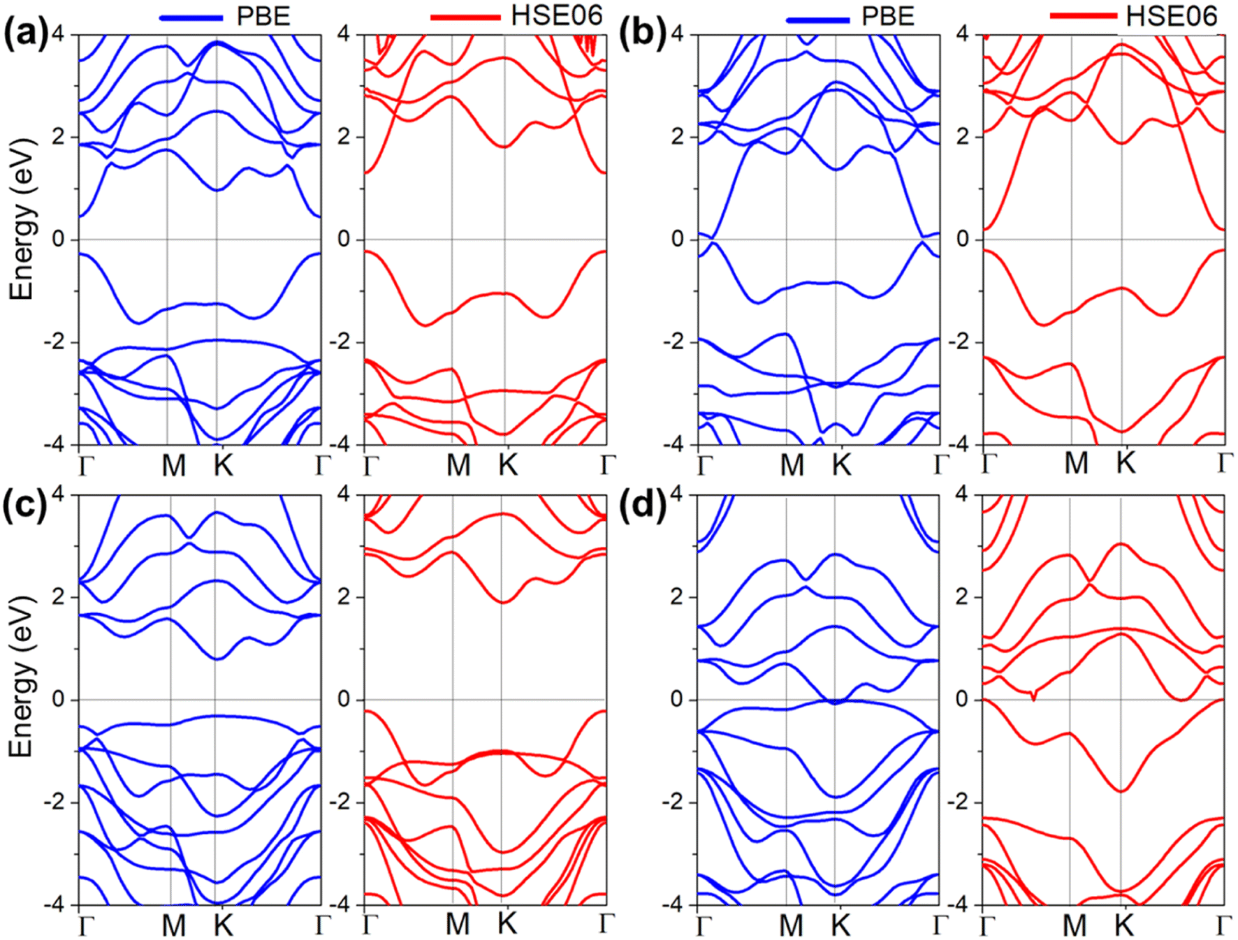 | ||
| Fig. 6 Band structures of QL-Al2SO3/MoSO heterostructures with the O (a) and S atom (b) surface of MoSO connected with the Aloct termination of QL-Al2O3 at the PBE (blue curves) and HSE06 (red curves) levels. The Fermi level is set to zero and depicted by the black line. Band structures of QL-Al2SO3/MoSO heterostructures with the S (c) and O atom (d) surface of MoSO connected with the Altet termination of QL-Al2O3. | ||
When the S atom of MoSO connects with Altet termination of QL-Al2O3, the CBM and VBM of the QL-Al2O3/MoSO heterostructure are located at the K-point. The band-gap of the QL-Al2O3/MoSO heterostructure is calculated to be 2.615 (4.179) eV at the PBE (HSE06), respectively, as shown in Fig. 6(c). When the O atom of MoSO connects with Altet termination of QL-Al2O3, both the CBM and VBM (near the K-point) cross the EF by PBE calculations as shown in Fig. 6(d). As a comparison, the Altet–O heterostructure is the most energy-favorable configuration, as shown in Fig. 2. The energy of Altet–S, Aloct–O, and Aloct–S heterostructure configurations is higher by 0.053, 0.065, and 0.061 eV per unit than that of the Altet–O heterostructure. Although the QL-Al2O3 and Janus MoSO monolayers are indirect bandgap semiconductors, it is interesting to find that QL-Al2O3/MoSO heterostructures are a direct band gap semiconductor or metal depending on the stacking method. Why do the band-structures in QL-Al2O3/MoSO heterostructures change with different stacking models? Next, the detailed electric properties of four heterostructures are analyzed for explaining the reason based on the PBE level.
When the Aloct termination of QL-Al2O3 connects with the MoSO surface (S or O) atom, the weighted band-structure and layer-resolved PDOS of two kinds of QL-Al2O3/MoSO heterostructures are compared with those of single QL-Al2O3 and MoSO monolayers, and the CBM from QL-Al2O3 in two QL-Al2O3/MoSO heterostructures comes near the EF, even crossing the EF when the Aloct termination connects with O and S atoms of the MoSO surface, as shown in Fig. 7(a), (b), (d) and (e), respectively. From band alignment, the CBM in QL-Al2O3 means that it got electrons from the MoSO monolayer when a heterostructure was formed. On comparing the different energy level positions of the CBM (VBM) in two QL-Al2O3/MoSO heterostructures, we can assume that there are more electrons (holes) transferred from MoSO to QL-Al2O3 when QL-Al2O3 connects with S rather than O atoms of the MoSO surface.
 | ||
| Fig. 7 Electric properties of QL-Al2SO3/MoSO heterostructures with the O (a)–(c) and S (d)–(f) surfaces of MoSO connected with the Aloct termination of QL-Al2O3. (a) Weighted band structure of the QL-Al2SO3/MoSO heterostructure. The blue, green and red color codings represent the contribution weights from Al, Mo and O atoms, respectively. The Fermi level is set to zero and depicted by the dashed line. (b) The layer-resolved PDOS of Al and Mo atoms along the z axis. The atom in each layer is labeled by number. (c) The planar-averaged electrostatic potential for QL-Al2O3/MoSO heterostructures along the z-axis. (g) and (i) The charge density difference of QLs-Al2O3/MoSO with the O and S surfaces of MoSO connected with the Aloct termination of QL-Al2O3. The blue and yellow regions represent electron depletion and accumulation, respectively. The isosurface values are set at 0.0003 e Å−1. (h) and (j) Schematic diagram illustrates the charge transfer mechanism between QLs-Al2O3 and MoSO layers. The higher yellow and green slabs in (j) compared with those in (h) represent the increased holes and electrons on the two surfaces in this QL-Al2O3/MoSO heterostructure. | ||
The interface charge transfer in two QL-Al2O3/MoSO heterostructures in Fig. 7(g) and (i) is obviously different: (1) the interfacial transferred charge is larger in the second heterostructure (Fig. 7(i)) than in the first heterostructure (Fig. 7(g)). (2) The electrons are transferred unidirectionally from MoSO to the QL-Al2O3 layer through the interface just in the second heterostructure, while two sets of interface charge transfer are present in the first heterostructure. (3) The subsequent behavior of transferred charge at the interface is different. The transferred charge spreads over the whole heterostructure and is not just located at the interface in the second heterostructure. In the first heterostructure, interface transferred charge just stays on S termination of MoSO and O termination of QL-Al2O3 at the interface. (4) From the above three differences, the driving force of interface charge transfer is different in two heterostructures. Next, we focus on the driving force of interface charge transfer.
The polarization direction arrangement of two QL-Al2O3/MoSO heterostructure configurations is different. When the O atom of MoSO connected with the Aloct termination, the intrinsic polarization direction inside QL-Al2O3 and MoSO is opposite. When the S atom of MoSO connected with the Aloct termination, the intrinsic polarization direction inside QL-Al2O3 and MoSO is the same. Compared with the polarization arrangement, the total electrostatic potential distribution shows two different situations. From the leftmost to the rightmost surface, the total potential across the QL-Al2O3/MoSO heterostructure increases first and then decreases, as shown in Fig. 7(c), while the total potential across the QL-Al2O3/MoSO heterostructure decreases step-like gradually, as shown in Fig. 7(f).
The surface charge distribution of the heterostructure is verified from the layer-resolved PDOS (induced charge) and the electrostatic potential distribution (bound charge). When the S atom of MoSO connects with the Aloct termination, the electrons and the holes are located at the rightmost and leftmost surfaces. In this configuration, the negative and positive polarization (bound) charges are accompanied by the holes and electrons as shown in Fig. 7(j). How is the surface charge distribution formed? The existence of a potential difference (Δϕ) represents the polarization strength or the number of polarization charges, which provides the driving force of interface charge transfer between QL-Al2O3 and MoSO layers. In addition, the interfacial transferred electron (or hole) will move to the outside surfaces driven by the inner polarization electric field in this heterostructure configuration. The electrons flow unidirectionally from a higher electrostatic potential to a lower electrostatic potential through the whole QL-Al2O3/MoSO heterostructure. When the O atom of MoSO connects with the Aloct termination, since the inner polarization electric fields in QL-Al2O3 and MoSO are opposite, both monolayers want to get electrons (holes) from another monolayer, so there is little electron (hole) flow through the interface. Since the highest electrostatic potential is located at the interface, there are double-directional electron (or holes) transfer processes through the interface.
The polarization electric field across two monolayers in the second heterostructure (Fig. 7(i) and (j)) provides the driving force for unidirectional charge transfer, while in the first heterostructure (Fig. 7(g)and (h)), there is no polarization electric field across the two monolayers. The uneven distribution of free charge (hole) number or polarization (bound) charge on both sides of the interface leads to the existence of an interface electric field. Corresponding, the direction of interface electric field is from MoSO to QL-Al2O3, since the total polarization electric field point from QL-Al2O3 to MoSO. The interface electric field in the polarization same-direction arrangement heterostructure is eliminated by the inner polarization electric field.
The changing band alignment in two heterostructures means different surface charge distributions and interface charge transfers. As shown in Fig. 8(c) and (g), the interface charge transfer in two heterostructures is surely different: (1) the amount of interfacial transferred charge is lower in the first heterostructure (Fig. 8(g)) than in the second heterostructure (Fig. 8(i)). (2) The electrons are transferred unidirectionally from QL-Al2O3 to MoSO through the interface in the second heterostructure, and not in the first heterostructure. (3) The transferred charge spreads over the whole heterostructure and is not just located at the interface S termination of MoSO and O termination of QL-Al2O3 in the second heterostructure. The interfacial transferred charge is just located at the interface in the first heterostructure.
 | ||
| Fig. 8 Electric properties of QL-Al2SO3/MoSO heterostructures with the S (a)–(c) and O (d)–(f) surfaces of MoSO connected with the Altet termination of QL-Al2O3. (g) and (i) depict the charge density difference of QLs-Al2O3/MoSO with the S and O surfaces of MoSO connected with the Altet termination of QL-Al2O3. (h) and (j) schematically depict the charge transfer process of QLs-Al2O3/MoSO in the process of S and O surfaces of MoSO connected with the Altet termination of QL-Al2O3. The blue and yellow regions represent electron depletion and accumulation, respectively. | ||
The polarization direction arrangement and the total electrostatic potential distribution of two QL-Al2O3/MoSO heterostructure configurations are different. From the leftmost to the rightmost surface, the total potential across the QL-Al2O3/MoSO heterostructure decreases first and then increases as shown in Fig. 8(c), while the total potential across the QL-Al2O3/MoSO heterostructure decreases gradually as shown in Fig. 8(f).
When the O atom of MoSO connects with the Altet termination, the electron (hole) and positive (negative) bound charge are located at the rightmost (leftmost) surface as shown in Fig. 8(i) and (j). The existence of Δϕ represents the polarization electric field, which provides the driving force of unidirectional charge transfer. When the S atom of MoSO connects with the Altet termination, the highest and lowest electrostatic potential distribution is located on the leftmost surface of QL-Al2O3 and the interface between QL-Al2O3 and MoSO monolayers. The electrons flow from a high electrostatic potential to a low electrostatic potential in this heterostructure, while the transferred charge through the interface is still low, because of the existence of an interface electric field. Corresponding, the direction of interface electric field is from QL-Al2O3 to MoSO, since the total polarization electric field point from MoSO to QL-Al2O3. The interface electric field in the polarization same-direction arrangement heterostructure is eliminated by the inner polarization electric field.
In summary, there are three types of interfacial charge transfer processes with different polarization arrangements in QL-Al2O3/MoSO heterostructures. The polarization direction arrangement and electrostatic potential distribution decide the direction of charge transfer, which will induce different surface charge distributions and band-structures of heterostructures. For the same-direction polarization heterojunction, the potential distribution is monotonically decreased, and the polarization electric field drives unidirectional transferred charges to accumulate at the surface atoms, which result in energy level shifting and the presence of metallicity in the QL-Al2O3/MoSO heterostructure. For the opposite-direction polarization heterojunction, the potential distribution is not monotonically decreased, and the interface transferred charge is low and trapped at the interface, since there is no total electric field through the heterostructure. Correspondingly, the charge distribution of two monolayer surfaces changes a little, and the electric properties keep the semiconductor in this QL-Al2O3/MoSO heterostructure.
The Aloct termination of QL-Al2O3 has connected with the MoSO surface (S or O) atom. The band structures and layer-resolved PDOS of two QLs-Al2O3/2MoSO heterostructures have shown metallicity. When the O atom of MoSO connects with QL-Al2O3, the layer-resolved PDOS clearly shows that both the VBM (from the middle MoSO layer) and CBM (from the rightmost MoSO layer) cross the EF as shown in Fig. 9(b). When the S atom of MoSO connects with QL-Al2O3, the layer-resolved PDOS clearly shows that both the VBM (from the leftmost MoSO layer) and CBM (from the rightmost QL-Al2O3) cross the EF as shown in Fig. 9(e).
 | ||
| Fig. 9 Electric properties of QL-Al2SO3/2MoSO heterostructures with the S (a)–(c) and O (d)–(f) surfaces of MoSO connected with the Aloct termination of QL-Al2O3. (g), (h) and (i), (j) depict the charge density difference of two QLs-Al2O3/2MoSO with the O and S surfaces of MoSO connected with the Aloct termination of QL-Al2O3. The blue and yellow regions represent electron depletion and accumulation, respectively. | ||
The different surface charge distributions of two QLs-Al2O3/2MoSO heterostructures correspond to different interface charge transfers between QLs-Al2O3 and two MoSO monolayers. For verifying the interfacial charge transfer process, two kinds of definitions of charge density difference of QL-Al2O3/2MoSO heterostructures are shown in Fig. 9(g), (h) and (i), (j). First, two MoSO layers are defined as one unit.60 Second, two MoSO monolayers are defined as separated monolayers.
The interface charge density differences of two QL-Al2O3/2MoSO heterostructures are different: (1) the amount of interfacial transferred charge is low in the first heterostructure (Fig. 9(g)) compared to in the second heterostructure (Fig. 9(i)). (2) The electrons (or holes) are transferred unidirectionally from left MoSO to QL-Al2O3 in the second heterostructure, while not in the first heterostructure. (3) The interface transferred charge spreads over the whole heterostructure and is not just located at the interface atoms in the second heterostructure. Here, since two MoSO monolayers are one unit, we can clearly see the unidirectional transfer of electrons from the left interface (left-MoSO/middle-MoSO) to the right interface (middle-MoSO/QL-Al2O3) by comparing two kinds of charge density differences.
The polarization direction and electrostatic potential distribution across two QLs-Al2O3/2MoSO heterostructures in Fig. 9(c) and (f) are consistent with that of the two QLs-Al2O3/2MoSO heterostructures in Fig. 7(c) and (f). For the same-direction polarization arrangement QLs-Al2O3/2MoSO heterostructure, the total potential across the QL-Al2O3/2MoSO heterostructure decreases gradually from the leftmost MoSO to the rightmost QL-Al2O3 surface as shown in Fig. 9(c). The electrons flow unidirectionally from the high potential (left-MoSO) layer to the low potential (QL-Al2O3) layer. Correspondingly, metallicity in this QL-Al2O3/2MoSO heterostructure originates from the increased surface charge induced by unidirectional charge transfer. For opposite-direction polarization QLs-Al2O3/2MoSO heterostructures, the highest electron potential is located at the interface between QLs-Al2O3 and the middle-MoSO monolayer. The charge transfer through the QLs-Al2O3/middle-MoSO interface is low and double-directional, while the potential distribution across the MoSO bilayer plays a major role in determining the metallicity of this QL-Al2O3/2MoSO as shown in Fig. 9(c). The electrons flow unidirectionally from a higher electrostatic potential (middle-MoSO) to a lower electrostatic potential (left-MoSO) as shown in Fig. 9(h), resulting in the shifting of the CBM (VBM) to EF on the left (middle)-MoSO layer.
The Altet termination of QL-Al2O3 has connected with the MoSO surface (S or O) atom. The band-structure of the two QLs-Al2O3/2MoSO has shown metallicity as shown in Fig. 10(a) and (d). When the S atom of MoSO connects with QL-Al2O3, both the CBM (from the middle-MoSO layer) and VBM (from the right-MoSO layer) cross the EF as shown in Fig. 10(b). When the O atom of MoSO connects with QL-Al2O3, both the VBM (from the leftmost QL-Al2O3 layer) and CBM (from the right-MoSO layer) cross the EF as shown in Fig. 10(e).
 | ||
| Fig. 10 Electric properties of QL-Al2SO3/2MoSO heterostructures with the S (a)–(c) and O (d)–(f) surfaces of MoSO connected with the Altet termination of QL-Al2O3. (g), (h) and (i), (j) depict the charge density difference of QLs-Al2O3/2MoSO with the S and O surfaces of MoSO connected with the Altet termination of QL-Al2O3. The blue and yellow regions represent electron depletion and accumulation, respectively. | ||
When the S atom of MoSO connects with the Altet termination, the potential distribution in MoSO bilayers play a major role in determining the electric properties of QL-Al2O3/2MoSO. The metallicity originates from 2MoSO because of the unidirectional charge transfer between two MoSO monolayers as shown in Fig. 10(h). When the O atom of MoSO connects with the Altet termination, the intrinsic polarization direction inside QL-Al2O3 and 2MoSO is the same. From the leftmost QL-Al2O3 to the rightmost MoSO surface, the total potential across the QL-Al2O3/2MoSO heterostructure decreases gradually as shown in Fig. 10(f). The metallicity in this heterostructure originates directly from the increased surface charge, induced by unidirectional charge transfer through the heterostructure. The interface charge transfer process of QL-Al2O3/2MoSO heterostructures is schematically summarized in Fig. 11.
 | ||
| Fig. 11 (a–d) Schematic diagram illustrates the interface charge transfer process in QL-Al2O3/2MoSO heterostructures with different polarization arrangements. (b and d) For the same-direction polarization arrangement, the polarization electric field drives the unidirectional electron and hole transfer through the whole heterostructure. The increased surface charge is shown with the higher green and yellow slabs. The black arrow indicates the intrinsic inner polarization electric field. The red arrow indicates the interface electric field. | ||
4. Discussion
4.1 The charge and electric field distribution of heterostructures
The reversable polarization induced band alignment transition has been proposed in 2D non-polar/polar and polar/polar heterostructures in previous research studies (Table 1). In addition, for non-polar/non-polar heterostructures, the semiconductor-to-metal transition process usually occurs under an external electric field or strain (Table 1). In this work, we propose that the evolution of the band structure in heterostructures stems from the increased or decreased surface charge distribution. Both the external electric field (in non-polar/non-polar heterostructures) and polarization electric field (in non-polar/polar and polar/polar heterostructures) affect the interface charge transfer and surface charge distribution, resulting in the adjustable band structure of the heterostructures. When we consider the evolution of electric properties of the 2D vdWs heterostructure, the surface charge distribution (past, present, and future) of the heterostructure should be analyzed. The difference between the past and present surface charge distribution of the heterostructure corresponds to the first stage interface charge transfer process. The difference between the present and future surface charge distribution of heterostructures corresponds to the second stage interface charge transfer process. So, it is important to focus on the present surface charge distribution of the heterostructure, which will decide the build-in electric field (inter-layer and inner-layer) distribution.According to the existence of the polarization (bound) charge of monolayers, we classify the 2D vdWs heterostructures into three kinds. Correspondingly, the electrostatic potential distributions across the 2D heterostructures are shown in Fig. 12. For non-polar/non-polar heterostructure, there is no Δϕ across the 2D heterostructures. For a non-polar/polar heterostructure and polar/polar heterostructure, there is Δϕ across the 2D heterostructures. The electrostatic potential distribution across the heterostructure not only depicts the spatial charge distribution, but also the electric field distribution, which decides the interface charge transfer in the first and second stage.
 | ||
| Fig. 12 (a–f) The planar-averaged electrostatic potential distribution across two monolayers of 2D vdWs heterostructures. The green arrow indicates the direction of the interface electron transfer. The black arrow indicates the intrinsic inner polarization electric field. | ||
For a non-polar/non-polar heterostructure, the zero Δϕ means the charge distribution of heterostructures is even after two layers are connected. So, there is no built-in electric field driving the second stage interface charge transfer. For a non-polar/polar heterostructure, the Δϕ is not zero. There are two types of interfacial charge transfer processes as shown in Fig. 12(b) and (c). The interfacial charge transfer direction can be judged by the electrostatic potential distribution, the electrons flow from a higher potential to a low potential, and the built-in polarization electric field provides the driving force for the charge transfer through the interface in the first stage.
For a polar/polar heterostructure, there are three types of interfacial charge transfer processes. When the polarization directions of two monolayers are the same as shown in Fig. 12(d), the spatial charge and electric field distribution are similar to that of a non-polar/polar heterostructure. When the polarization directions of the two monolayers are opposite as shown in Fig. 12(e) and (f), both the built-in polarization and interface electric field affect the interfacial charge transfer processes. There are two common rules from the above results. First, the total potential difference across the heterostructure depends on which side (higher or lower potential) of the polar material is connected to the added 2D material. Second, the total potential difference across the heterostructure obeys the polar monolayer with a larger Δϕ (polarization strength). Specifically, the Δϕ across QL-Al2O3 is larger than the Δϕ across the MoSO monolayer or bilayer. So, the electrostatic potential distribution of QL-Al2O3 plays a main role in deciding the interface charge transfer direction.
4.2 The charge redistribution of heterostructures
At present, there are different heterostructure photocatalysts according to different interface charge (photoexcited carrier) transfer mechanisms. The charge (photoexcited) transfer direction is opposite in type-II and Z-scheme heterostructure photocatalysts, though they have similar band alignments as shown in Fig. 13(a) and (c). By showing the spatial charge and built-in electric field (polarization or the interface) distribution across the heterostructure, we will judge the charge redistribution and interface charge transfer of the heterostructure. The electric field distribution decides the second stage interface charge transfer process of the heterostructure under external stimulation (light irradiation). | ||
| Fig. 13 (a–e) Schematic diagram illustrates the interface charge transfer mechanism of different 2D heterostructure photocatalysts. The larger dotted green arrows represent the first stage interface electron transfer. The smaller green arrows represent the second stage interface electron transfer. For clarifying the spatially separated surface charge distribution of 2D materials, the surface positive and negative polarization charge (“+” and “−”) and the accompanying induced charge distribution (electron and hole) are shown in the system. Both the intrinsic polarization electric field (black arrow) and interface electric field (red arrow) drive the charge transfer. The charge transfer in a polar-PN heterostructure is a two-step process: first, electrons and holes are transferred to the other layer at the interface. Second, the transferred interface electrons and holes will continue to move to the outside surface. | ||
For type-II and Z-scheme heterostructures, the zero Δϕ means no polarization electric field exists, while the built-in interface electric field (the uneven charge distribution) exists in Z-scheme heterostructures. The difference between type-II and polar-PN heterostructures (same polarization direction arrangement) is the existence of a built-in polarization electric field, since the Δϕ means the spatially separated polarization charge distribution in the heterostructure. Similarly, the difference between Z-scheme and S-scheme heterostructures is the existence of a built-in polarization electric field. The difference between polar-PN and S-scheme heterostructures is the existence of a built-in interface electric field.
5. Conclusions
In summary, we have investigated the structural and electronic properties of 2D QL-Al2O3, Janus MoSO monolayers and QL-Al2O3/MoSO heterostructures. The phonon spectrum and AIMD analysis indicate that QL-Al2O3 and Janus MoSO monolayers are thermally and dynamically stable. QL-Al2O3 and MoSO monolayers are semiconductors with an indirect bandgap, while the QL-Al2O3/MoSO heterostructures become direct band gap semiconductors or metals depending on the stacking method. In essence, the band alignment of QL-Al2O3/MoSO heterostructures is determined by the polarization arrangement across the QL-Al2O3/MoSO heterostructures. When the polarization direction of stacked QL-Al2O3 and MoSO monolayers is the same, this QL-Al2O3/MoSO heterostructure shows metallicity. Metallicity directly originates from increased surface induced (free) charges, which are driven by the polarization electric field. When the polarization direction of stacked QLs-Al2O3 and MoSO monolayers is opposite, the unidirectional charge transfer route disappears. There is little charge transfer through the interface, and this QL-Al2O3/MoSO heterostructure will still be a semiconductor. The evolution of band alignment, surface charge redistribution and interface charge transfer across QL-Al2O3/MoSO heterostructures are synchronous.We also classify the potential distribution alignment in 2D vdWs heterostructures according to the intrinsic polarization of monolayers. The total potential difference across the polar heterostructures decides the charge transfer direction. Our work reveals the basic connection between the band alignment and charge distribution in 2D polarized heterostructure systems. The understanding of intriguing electric properties of 2D heterostructures promotes their applications in photocatalysts and nano-optoelectronic devices.
Author contributions
Xinli Wang: conceptualization, methodology, writing – original draft. Juping Xu: investigation, validation. Peng-Fei Liu: investigation, validation. Bao-tian Wang: software, validation. Wen Yin: supervision, funding acquisition, writing – review & editing.Conflicts of interest
There are no conflicts of interest to declare.Acknowledgements
This work was financially supported by the National Key Research and Development Program of China (Grant No. 2020YFA0406201 and 2021YFA1600701).References
- P. Ganguly, M. Harb, Z. Cao, L. Cavallo, A. Breen, S. Dervin, D. D. Dionysiou and S. C. Pillai, ACS Energy Lett., 2019, 4, 1687–1709 CrossRef CAS.
- G. Z. Wang, J. L. Chang, W. Y. Tang, W. J. Xie and Y. S. Ang, J. Phys. D: Appl. Phys., 2022, 55, 293002 CrossRef.
- C. S. Liu, H. W. Chen, S. Y. Wang, Q. Liu, Y.-G. Jiang, D. W. Zhang, M. Liu and P. Zhou, Nat. Nanotechnol., 2020, 15, 545–557 CrossRef CAS PubMed.
- R. G. Quhe, L. Xu, S. Q. Liu, C. Yang, Y. Y. Wang, H. Li, J. Yang, Q. H. Li, B. W. Shi, Y. Li, Y. Y. Pan, X. T. Sun, J. Z. Li, M. Y. Weng, H. Zhang, Y. Guo, L. Q. Xu, H. Tang, J. C. Dong, J. B. Yang, Z. Y. Zhang, M. Lei, F. Pan and J. Lu, Phys. Rep., 2021, 938, 1–72 CrossRef CAS.
- Q. L. Zhao, Z. J. Xie, Y.-P. Peng, K. Y. Wang, H. D. Wang, X. N. Li, H. W. Wang, J. S. Chen, H. Zhang and X. B. Yan, Mater. Horiz., 2020, 7, 1495 RSC.
- Z. C. Zhou, F. Y. Yang, S. Wang, L. Wang, X. F. Wang, C. Wang, Y. Xie and Q. Liu, Front. Phys., 2022, 17(2), 23204 CrossRef.
- K. H. Liao, P. X. Lei, M. L. Tu, S. W. Luo, T. Jiang, W. J. Jie and J. H. Hao, ACS Appl. Mater. Interfaces, 2021, 13, 32606–32623 CrossRef CAS PubMed.
- S. Batool, M. Idrees, S.-R. Zhang, S.-T. Han and Y. Zhou, Nanoscale Horiz., 2022, 7, 480 RSC.
- C. L. Tan, Z. D. Liu, W. Huang and H. Zhang, Chem. Soc. Rev., 2015, 44, 2615 RSC.
- T. Y. Jin, J. Y. Mao, J. Gao, C. Han, K. P. Loh, A. T. S. Wee and W. Chen, ACS Nano, 2022, 16, 13595–13611 CrossRef CAS PubMed.
- Z. J. Ma, Q. Zhang and N. Valanoor, Appl. Phys. Rev., 2020, 7, 041316 CAS.
- S. M. Poh, S. J. R. Tan, H. Wang, P. Song, I. H. Abidi, X. X. Zhao, J. D. Dan, J. S. Chen, Z. T. Luo, S. J. Pennycook, A. H. C. Neto and K. P. Loh, Nano Lett., 2018, 18, 6340–6346 CrossRef CAS PubMed.
- S. Q. Zhang, R. Xu, N. N. Luo and X. L. Zou, Nanoscale, 2021, 13, 1398 RSC.
- N. Sethulakshmi, A. Mishra, P. M. Ajayan, Y. Kawazoe, A. K. Roy, A. K. Singh and C. S. Tiwary, Mater. Today, 2019, 27, 107–122 CrossRef CAS.
- Y. R. Su, X. L. Li, M. Zhu, J. Zhang, L. You and E. Y. Tsymbal, Nano Lett., 2021, 21, 175–181 CrossRef CAS PubMed.
- Z. Yan, Z. Y. Li, Y. L. Han, Z. H. Qiao and X. H. Xu, Phys. Rev. B, 2022, 105, 075423 CrossRef CAS.
- X. P. Liu, C. H. Shen, X. P. Li, T. X. Wang, M. J. He, L. Li, Y. Wang, J. B. Li and C. X. Xia, Nanoscale, 2022, 14, 5454 RSC.
- H. J. Li, Y. Zhou, W. G. Tu, J. H. Ye and Z. G. Zou, Adv. Funct. Mater., 2015, 25, 998–1013 CrossRef CAS.
- J. X. Low, J. G. Yu, M. Jaroniec, S. Wageh and A. A. A. Ghamdi, Adv. Mater., 2017, 29, 1601694 CrossRef PubMed.
- Q. L. Xu, L. Y. Zhang, J. G. Yu, S. Wageh, A. A. A. Ghamdi and M. Jaroniec, Mater. Today, 2018, 21, 1042–1063 CrossRef CAS.
- L. Y. Zhang, J. J. Zhang, H. G. Yu and J. G. Yu, Adv. Mater., 2022, 34, 2107668 CrossRef CAS PubMed.
- Q. L. Xu, L. Y. Zhang, B. Cheng, J. J. Fan and J. G. Yu, Chem, 2020, 6, 1543–1559 CAS.
- Y. B. Lee, Y. B. Hwang and Y.-C. Chung, ACS Appl. Mater. Interfaces, 2015, 7, 7163–7169 CrossRef CAS PubMed.
- Z. F. Xie, F. W. Sun, R. Yao, Y. Zhang, Y. H. Zhang, Z. H. Zhang, J. B. Fan, L. Ni and L. Duan, Appl. Surf. Sci., 2019, 475, 839–846 CrossRef CAS.
- Z. H. Zhang, Y. Zhang, Z. F. Xie, X. Wei, T. T. Guo, J. B. Fan, L. Ni, Y. Tian, J. Liu and L. Duan, Phys. Chem. Chem. Phys., 2019, 21, 5627 RSC.
- D. H. Wang, W. W. Ju, T. W. Li, Q. X. Zhou, Y. Zhang, Z. J. Gao, D. W. Kang, H. S. Li and S. J. Gong, J. Phys.: Condens. Matter, 2021, 33, 045501 CrossRef CAS PubMed.
- R. Zhang, Y. Zhang, X. Wei, T. T. Guo, J. B. Fan, L. Ni, Y. J. Weng, Z. D. Zha, J. Liu, Y. Tian, T. Li and L. Duan, Appl. Surf. Sci., 2020, 528, 146782 CrossRef CAS.
- Z. Wang, Y. Zhang, X. Wei, T. T. Guo, J. B. Fan, L. Ni, Y. J. Weng, Z. D. Zha, J. Liu, Y. Tian, T. Li and L. Duan, Phys. Chem. Chem. Phys., 2020, 22, 9647 RSC.
- Z. Wang, F. W. Sun, J. Liu, Y. Tian, Z. H. Zhang, Y. Zhang, X. Wei, T. T. Guo, J. B. Fan, L. Ni and L. Duan, Phys. Chem. Chem. Phys., 2020, 22, 20712 RSC.
- H. Qiao, Y. Zhang, Z.-H. Yan, L. Duan, L. Ni and J.-B. Fan, Appl. Surf. Sci., 2022, 604, 154602 CrossRef CAS.
- N. H. Song, Y. S. Wang, Z. M. Yuan and F. Wang, Appl. Surf. Sci., 2022, 598, 153830 CrossRef CAS.
- J. P. Li, Z. M. Huang, W. Ke, J. Yu, K. Ren and Z. R. Dong, J. Alloys Compd., 2021, 866, 158774 CrossRef CAS.
- X. P. Li, G. R. Jia, J. Du, X. H. Song, C. X. Xia, Z. M. Wei and J. B. Li, J. Mater. Chem. C, 2018, 6, 10010 RSC.
- X. Chen, Z.-Z. Lin and M. Ju, Phys. Status Solidi RRL, 2018, 12, 1800102 CrossRef.
- Y. C. Fan, X. K. Ma, X. B. Liu, J. R. Wang, H. Q. Ai and M. W. Zhao, J. Phys. Chem. C, 2018, 122, 27803–27810 CrossRef CAS.
- Y. F. Jia, X. Wei, Z. H. Zhang, J. Liu, Y. Tian, Y. Zhang, T. T. Guo, J. B. Fan, L. Ni, L. J. Luan and L. Duan, CrystEngComm, 2021, 23, 1033–1042 RSC.
- W. Li, T. X. Wang, X. Q. Dai, Y. Q. Ma and Y. Tang, J. Alloys Compd., 2017, 705, 486–491 CrossRef CAS.
- H. B. Shu, Y. Wang and M. L. Sun, Phys. Chem. Chem. Phys., 2019, 21, 15760 RSC.
- L. Huang, N. J. Huo, Y. Li, H. Chen, J. H. Yang, Z. M. Wei, J. B. Li and S.-S. Li, J. Phys. Chem. Lett., 2015, 6, 2483–2488 CrossRef CAS PubMed.
- H. Zhang, M. Pei, B. Y. Liu, Z. L. Wang and X. Zhao, Phys. Chem. Chem. Phys., 2022, 24, 19853 RSC.
- X. P. Hong, J. Kim, S.-F. Shi, Y. Zhang, C. H. Jin, Y. H. Sun, S. Tongay, J. Q. Wu, Y. F. Zhang and F. Wang, Nat. Nanotechnol., 2014, 8, 682–686 CrossRef PubMed.
- D. Huang and E. Kaxiras, Phys. Rev. B, 2016, 94, 241303(R) CrossRef.
- X. H. Meng, Y. Q. Shen, J. J. Liu, L. L. Lv, X. Yang, X. Gao, M. Zhou, X. Y. Wang, Y. D. Zheng and Z. X. Zhou, Appl. Catal., A, 2021, 624, 118332 CrossRef CAS.
- J. Z. Xuan, L. J. Luan, J. He, H. X. Chen, Y. Zhang, J. Liu, Y. Tian, X. Wei, Y. Yang, J. B. Fan and L. Duan, J. Lumin., 2022, 251, 119256 CrossRef CAS.
- T. Ayadi, L. Debbichi, M. Badawi, M. Said, D. Rocca and S. Lebègue, Appl. Surf. Sci., 2021, 538, 148066 CrossRef CAS.
- B. Zhou, S.-J. Gong, K. Jiang, L. P. Xu, L. Q. Zhu, L. Y. Shang, Y. W. Li, Z. G. Hu and J. H. Chu, J. Phys.: Condens. Matter, 2020, 32, 055703 CrossRef CAS PubMed.
- B. Zhou, K. Jiang, L. Y. Shang, J. Z. Zhang, Y. W. Li, L. Q. Zhu, S.-J. Gong, Z. G. Hu and J. H. Chu, J. Mater. Chem. C, 2020, 8, 11160 RSC.
- Z. Wang and W. G. Zhu, ACS Appl. Electron. Mater., 2021, 3, 5114–5123 CrossRef CAS.
- Y. F. Shao, Q. Wang, H. Pan and X. Q. Shi, Adv. Electron. Mater., 2020, 6, 1900981 CrossRef CAS.
- B. Y. Wang, J. Ning, J. C. Zhang, D. Wang and Y. Hao, Phys. E, 2022, 143, 115360 CrossRef CAS.
- M. J. Yang, H. B. Shu, Y. Y. Li, D. Cao and X. S. Chen, Adv. Electron. Mater., 2022, 8, 2101022 CrossRef CAS.
- H. Zhu, Y. Shen, Q. L. Fang, X. D. Yang, L. Chen and S. Q. Xu, Phys. Chem. Chem. Phys., 2022, 24, 15075 RSC.
- H. H. Chen, J. L. Zhao, X. Y. Wang, X. L. Chen, Z. F. Zhang and M. Y. Hua, Nanoscale, 2022, 14, 5551 RSC.
- D. C. Chen, X. L. Lei, Y. N. Wang, S. Y. Zhong, G. Liu, B. Xu and C. Y. Ouyang, Appl. Surf. Sci., 2019, 497, 143809 CrossRef CAS.
- B. Zhou, A. Y. Cui, L. C. Gao, K. Jiang, L. Y. Shang, J. Z. Zhang, Y. W. Li, S.-J. Gong, Z. G. Hu and J. H. Chu, Phys. Rev. Mater., 2021, 5, 125404 CrossRef CAS.
- X. P. Li, B. X. Zhai, X. H. Song, Y. Yan, J. B. Li and C. X. Xia, Appl. Surf. Sci., 2020, 509, 145317 CrossRef CAS.
- H. L. Liu, J. L. Ren, C. X. Zhang, M. S. Zhou, C. Y. He, J. Li, T. Ouyang, C. Tang and J. X. Zhong, J. Phys. D: Appl. Phys., 2020, 53, 405101 CrossRef CAS.
- J. Ding, D.-F. Shao, M. Li, L.-W. Wen and E. Y. Tsymbal, Phys. Rev. Lett., 2021, 126, 057601 CrossRef CAS PubMed.
- R. Peng, Y. D. Ma, S. Zhang, B. B. Huang, L. Z. Kou and Y. Dai, Mater. Horiz., 2020, 7, 504 RSC.
- X. L. Wang, J. P. Xu, J. G. Si, B. T. Wang and W. Yin, Appl. Surf. Sci., 2023, 610, 155614 CrossRef CAS.
- Y. J. Bai, R. F. Guan, H. Y. Zhang, Q. F. Zhang and N. Xu, Catal. Sci. Technol., 2021, 11, 542 RSC.
- Y. C. Fan, X. K. Ma, J. R. Wang, X. H. Song, A. Z. Wang, H. Liu and M. W. Zhao, Sci. Bull., 2020, 65, 27–34 CrossRef CAS PubMed.
- X. Gao, Y. Q. Shen, J. J. Liu, L. L. Lv, M. Zhou, Z. X. Zhou, Y. P. Feng and L. Shen, Appl. Surf. Sci., 2022, 599, 153942 CrossRef CAS.
- M. J. He, X. P. Li, X. Y. Liu, L. Li, S. Y. Wei and C. X. Xia, Phys. E, 2022, 142, 115256 CrossRef CAS.
- K. Ren, W. C. Tang, M. L. Sun, Y. Q. Cai, Y. Cheng and G. Zhang, Nanoscale, 2020, 12, 17281 RSC.
- X. T. Zhu, Y. Xu, Y. Cao, D. F. Zou and W. Sheng, Appl. Surf. Sci., 2022, 574, 151650 CrossRef CAS.
- Y. J. Bai, H. Y. Zhang, X. Q. Wu, N. Xu and Q. F. Zhang, J. Phys. Chem. C, 2022, 126, 2587–2595 CrossRef CAS.
- J. J. Liu, Y. Q. Shen, L. L. Lv, X. H. Meng, X. Gao, M. Zhou, Y. D. Zheng and Z. X. Zhou, Appl. Surf. Sci., 2022, 589, 153025 CrossRef CAS.
- B. Wang, X. T. Wang, H. K. Yuan, T. W. Zhou, J. L. Chang and H. Chen, Int. J. Hydrogen Energy, 2020, 45, 2785–2793 CrossRef CAS.
- X. Gao, Y. Q. Shen, J. J. Liu, L. L. Lv, M. Zhou, Z. X. Zhou, Y. P. Feng and L. Shen, Catal. Sci. Technol., 2022, 12, 3614 RSC.
- C.-F. Fu, R. Q. Zhang, Q. Q. Luo, X. X. Li and J. L. Yang, J. Comput. Chem., 2019, 40, 980–987 CrossRef CAS PubMed.
- S. Sannigrahi, A. Ghosh, B. Ball and P. Sarkar, J. Phys. Chem. C, 2022, 126, 20852–20863 CrossRef CAS.
- R. Xiong, Y. Shu, X. H. Yang, Y. G. Zhang, C. L. Wen, M. Anpo, B. Wu and B. S. Sa, Catal. Sci. Technol., 2022, 12, 3272–3280 RSC.
- M. Y. Cao, L. Ni, Z. Wang, J. Liu, Y. Tian, Y. Zhang, X. Wei, T. T. Guo, J. B. Fan and L. Duan, Appl. Surf. Sci., 2021, 551, 149364 CrossRef CAS.
- X. Huang, Z. G. Cui, X. M. Shu, H. Y. Dong, Y. K. Weng, Y. H. Wang and Z. H. Yang, Phys. Rev. Mater., 2021, 6, 034010 CrossRef.
- X. H. Niu, X. W. Bai, Z. B. Zhou and J. L. Wang, ACS Catal., 2020, 10, 1976–1983 CrossRef CAS.
- R. Q. Zhang, L. L. Zhang, Q. J. Zheng, P. F. Gao, J. Zhao and J. L. Yang, J. Phys. Chem. Lett., 2018, 9, 5419–5424 CrossRef CAS PubMed.
- X. X. Jiang, W. L. Xie, X. H. Xu, Q. Gao, D. M. Li, B. Cui, D. S. Liu and F. Y. Qu, Nanoscale, 2022, 14, 7292 RSC.
- G. Z. Wang, W. Y. Tang, C. P. Xu, J. He, Q. R. Zeng, W. J. Xie, P. Gao and J. L. Chang, Appl. Surf. Sci., 2022, 599, 153960 CrossRef CAS.
- G. Z. Wang, J. L. Chang, S.-D. Guo, W. K. Wu, W. Y. Tang, H. Guo, S. H. Dang, R. Wang and Y. S. Ang, Phys. Chem. Chem. Phys., 2022, 24, 25287 RSC.
- A. Q. Shi, D. Z. Sun, X. M. Zhang, S. L. Ji, L. L. Wang, X. Li, Q. Zhao and X. H. Niu, ACS Catal., 2022, 12, 9570–9578 CrossRef CAS.
- Y. C. Fan, B. Yang, X. H. Song, X. F. Shao and M. W. Zhao, J. Phys. D: Appl. Phys., 2018, 51(7pp), 395501 CrossRef.
- C. Fu, G. Z. Wang, Y. H. Huang, Y. Chen, H. K. Yuan, Y. S. Ang and H. Chen, Phys. Chem. Chem. Phys., 2022, 24, 3826 RSC.
- J. Wang, X. J. Zhang, X. H. Song, Y. C. Fan, Z. H. Zhang and M. W. Zhao, J. Phys. Chem. Lett., 2023, 14, 798–808 CrossRef CAS PubMed.
- Z. B. Zhou, X. H. Niu, Y. H. Zhang and J. L. Wang, J. Mater. Chem. A, 2019, 7, 21835–21842 RSC.
- X. Y. Liu, P. Cheng, X. H. Zhang, T. Shen, J. Liu, J.-C. Ren, H. Q. Wang, S. Li and W. Liu, J. Mater. Chem. A, 2021, 9, 14515 RSC.
- M. Yagmurcukardes and F. M. Peeters, Phys. Rev. B, 2020, 101, 155205 CrossRef CAS.
- X. Jin, Y.-Y. Zhang, S. T. Pantelides and S. X. Du, Nanoscale Horiz., 2021, 10, 1039 Search PubMed.
- R. Wischert, P. Laurent, C. Copéret, F. Delbecq and P. Sautet, J. Am. Chem. Soc., 2012, 134, 14430–14449 CrossRef CAS PubMed.
- C. Bara, E. Devers, M. Digne, A. F. L. Humblot, G. D. Pirngruber and X. Carrier, ChemCatChem, 2015, 7, 3422–3440 CrossRef CAS.
- M. Kulawik, N. Nilius and H.-J. Freund, Phys. Rev. Lett., 2006, 96, 036103 CrossRef CAS PubMed.
- J. H. Kwak, J. Z. Hu, D. H. Mei, C.-W. Yi, D. H. Kim, C. H. F. Peden, L. F. Allard and J. Szanyi, Science, 2009, 325, 1670–1673 CrossRef CAS PubMed.
- P. Raybaud, C. Chizallet, C. M. Maury, M. Digne, H. Toulhoat and P. Sautet, J. Catal., 2013, 308, 328–340 CrossRef CAS.
- L. Foppa, T. Margossian, S. M. Kim, C. Müller, C. Copéret, K. Larmier and A. C. Vives, J. Am. Chem. Soc., 2017, 139, 17128–17139 CrossRef CAS PubMed.
- M. Shekhar, J. Wang, W.-S. Lee, W. D. Williams, S. M. Kim, E. A. Stach, J. T. Miller, W. N. Delgass and F. H. Ribeiro, J. Am. Chem. Soc., 2012, 134, 4700–4708 CrossRef CAS PubMed.
- A. Zavabeti, J. Z. Ou, B. J. Carey, N. Syed, R. O. Trigg, E. L. H. Mayes, C. L. Xu, O. Kavehei, A. P. O'Mullane, R. B. Kaner, K. K. zadeh and T. Daeneke, Science, 2017, 358, 332–335 CrossRef CAS PubMed.
- K. S. Liu, H. R. Jin, L. W. Huang, Y. X. Luo, Z. H. Zhu, S. M. Dai, X. Y. Zhuang, Z. D. Wang, L. Huang and J. Zhou, Sci. Adv., 2022, 8, 2030 CrossRef PubMed.
- A. Stierle, F. Renner, R. Dosch, W. Drube and B. C. Cowie, Science, 2004, 303, 1652 CrossRef CAS PubMed.
- G. Kresse, M. Schmid, E. Napetschnig, M. Shishkin, L. Köhler and P. Varga, Science, 2005, 308, 1440 CrossRef CAS PubMed.
- J. H. Dycus, K. J. Mirrielees, E. D. Grimley, R. Kirste, S. Mita, Z. Sitar, R. Collazo, D. L. Irving and J. M. LeBeau, ACS Appl. Mater. Interfaces, 2018, 10, 10607–10611 CrossRef CAS PubMed.
- W. J. Ding, J. B. Zhu, Z. Wang, Y. F. Gao, D. Xiao, Y. Gu, Z. Y. Zhang and W. G. Zhu, Nat. Commun., 2017, 8, 14956 CrossRef CAS PubMed.
- C.-F. Fu, J. Y. Sun, Q. Q. Luo, X. X. Li, W. Hu and J. L. Yang, Nano Lett., 2018, 18, 6312–6317 CrossRef PubMed.
- Y. J. Ji, M. Y. Yang, H. P. Lin, T. J. Hou, L. Wang, Y. Y. Li and S.-T. Lee, J. Phys. Chem. C, 2018, 122, 3123–3129 CrossRef CAS.
- L. Ju, M. Bie, J. Shang, X. Tang and L. Z. Kou, J. Phys.: Mater., 2020, 3, 022004 CAS.
- M. J. Varjovi, M. Yagmurcukardes, F. M. Peeters and E. Durgun, Phys. Rev. B, 2021, 103, 195438 CrossRef CAS.
- V. V. On, D. K. Nguyen, J. G. Sanchez and D. M. Hoat, New J. Chem., 2021, 45, 20776 RSC.
- L. Zhang, Z. J. F. Yang, T. Gong, R. K. Pan, H. D. Wang, Z. N. Guo, H. Zhang and X. Fu, J. Mater. Chem. A, 2020, 8, 8813 RSC.
- L. Zhang, Y. Xia, X. D. Li, L. Y. Li, X. Fu, J. J. Cheng and R. K. Pan, J. Appl. Phys., 2022, 131, 230902 CrossRef CAS.
- W.-J. Yin, H.-J. Tan, P.-J. Ding, B. Wen, X.-B. Li, G. Teobaldi and L.-M. Liu, Mater. Adv., 2021, 2, 7543 RSC.
- T. Zheng, Y.-C. Lin, N. Rafizadeh, D. B. Geohegan, Z. H. Ni, K. Xiao and H. Zhao, ACS Nano, 2022, 16, 4197–4205 CrossRef CAS PubMed.
- Y. Park, C. Ahn, J.-G. Ahn, J. H. Kim, J. Jung, J. Oh, S. Ryu, S. Kim, S. C. Kim, T. Kim and H. Lim, ACS Nano, 2023, 17, 1196–1205 CrossRef CAS PubMed.
- M. Wang, S. H. Cai, C. Pan, C. Y. Wang, X. J. Lian, Y. Zhuo, K. Xu, T. J. Cao, X. Q. Pan, B. G. Wang, S. J. Liang, J. J. Yang, P. Wang and F. Miao, Nat. Electron., 2018, 1, 130–136 CrossRef CAS.
- G. Kresse and J. Furthmuller, Phys. Rev. B: Condens. Matter Mater. Phys., 1996, 54, 11169–11186 CrossRef CAS PubMed.
- W. Kohn and L. J. Sham, Phys. Rev., 1965, 140, A1133–A1138 CrossRef.
- P. e. Blöchl, Phys. Rev. B: Condens. Matter Mater. Phys., 1994, 50, 17953–17979 CrossRef PubMed.
- J. P. Perdew, K. Burke and M. Ernzerhof, Phys. Rev. Lett., 1996, 77, 3865–3868 CrossRef CAS PubMed.
- J. Heyd, G. E. Scuseria and M. Ernzerhof, J. Chem. Phys., 2003, 118, 8207–8215 CrossRef CAS.
- T. Sohier, M. Calandra and F. Mauri, Phys. Rev. B, 2017, 96, 075448 CrossRef.
- S. Nosé, J. Chem. Phys., 1984, 81, 511 CrossRef.
- V. Wang, N. Xu, J.-C. Liu, G. Tang and W.-T. Geng, Comput. Phys. Commun., 2021, 267, 108033 CrossRef CAS.
- K. Momma and F. Izumi, J. Appl. Crystallogr., 2011, 44, 1272–1276 CrossRef CAS.
- M.-Y. Liu, Y. He, Y. Mao and K. Xiong, Phys. Rev. B, 2022, 105, 035418 CrossRef CAS.
- S. Baroni, S. de Gironcoli, A. D. Corso and P. Giannozzi, Rev. Mod. Phys., 2001, 73, 515–562 CrossRef CAS.
| This journal is © The Royal Society of Chemistry 2023 |