
 Open Access Article
 This Open Access Article is licensed under a Creative Commons Attribution-Non Commercial 3.0 Unported Licence
Ge-alloyed kesterite thin-film solar cells: previous investigations and current status – a comprehensive review†
Romain
Scaffidi
 *abcd,
Gizem
Birant
abc,
Guy
Brammertz
abc,
Jessica
de Wild
abc,
Denis
Flandre
d and
Bart
Vermang
abc
*abcd,
Gizem
Birant
abc,
Guy
Brammertz
abc,
Jessica
de Wild
abc,
Denis
Flandre
d and
Bart
Vermang
abc
aIMO, Hasselt University, Wetenschapspark 1, 3590 Diepenbeek, Belgium. E-mail: romain.scaffidi@imec.be
bIMOMEC, imec, Wetenschapspark 1, 3590 Diepenbeek, Belgium
cEnergyVille 2, Thor Park 8320, 3600 Genk, Belgium
dICTEAM, UCLouvain, Place du Levant 3/L5.03.02, 1348 Louvain-la-Neuve, Belgium
First published on 14th June 2023
Abstract
The incorporation of Ge into kesterite thin-film absorbers for photovoltaic (PV) applications is thoroughly reviewed. Kesterite materials constitute a promising and critical raw material-free alternative to other inorganic thin-film PV compounds such as Cu(In,Ga)Se2 and CdTe. The interest in Ge alloying is to solve the critical open-circuit voltage (Voc) deficit for kesterite solar cells, which is still unresolved and under strong debate. First, the substitution of Sn with Ge from 0 to 100% in the composition of Cu2Zn(Sn1−x,Gex)(Sy,Se1−y)4 absorbers is largely discussed, with a complete overview on the existing literature. It is concluded that fine composition tuning is essential to ensure the Ge-induced enhancement of morphology and single-phase growth through a modified reaction pathway. In this regard, choosing between vacuum- and non vacuum-based deposition methods also plays a crucial role, since the former allows further up-scaling whereas the latter leads to higher thin-film quality. Second, at the solar cell level, Se-rich devices with less than 40% Ge currently exhibit the lowest Voc and fill factor deficits with the highest efficiencies beyond 13%. This is mainly due to defect and band tail compensation as well as a graded bandgap and enlarged crystalline grains. This study unveils encouraging prospects for Ge-boosted kesterite PV devices.
1 Introduction
Solar power has become an increasingly essential alternative to replace fossil fuels in the energy transition. Still, there remain many challenges for photovoltaics (PV) to become an even more affordable and widespread source of renewable energy. Thin-film solar cells recently gained particular interest due to their promising performance and high integration potential. Indeed, their lightweight, semi-transparent and flexible designs constitute strong assets for simpler and deeper PV integration into specific sectors such as building-integrated PV (BIPV), vehicle-integrated PV (VIPV), and agrivoltaics,1–5 among others. They also present advantages of lower material consumption, a short energy payback period and low-temperature production of large-area modules with tuneable properties.2,6–9The former aspect is especially critical since one of the most efficient thin-film PV technologies, i.e. Cu(In,Ga)Se2 (CIGSe)-based solar cells having a remarkable record power conversion efficiency (PCE) of 23.35%,10 greatly rely on scarce indium and gallium.11 This raises important questions about long-term sustainability and expansion of CIGSe PV, the answer to which may be found in kesterite materials, considered a relevant alternative that involves more abundant metals such as zinc and tin.2,7,8,12,13 Generally speaking, they have the I2-II-IV-VI4 chemical formula in which each number designates the group of the element with, for instance, I = Cu, Ag; II = Zn, Cd; IV = Sn, Ge; VI = S, Se. The best kesterite-based PV technology so far relies on (Ag,Cu)2ZnSn(S,Se)4 (ACZTSSe) as the active material with a “notable exception” record efficiency of 13.6%14 and a recently reported certified PCE nearly reaching the 14% limit.15 This is significantly lower than that for CIGSe and requires further work to understand the remaining limiting factors and counteract them.
Today, the main reason for the lower performance of kesterites is mostly attributed to their high open-circuit voltage deficit (Voc,def),2,7,8,12,13,16–19 the physical origin of which is still under strong debate. Overall, we distinguish three contributions to Voc,def arising from the bulk of the absorber: bandgap and potential fluctuations induced by Cu–Zn crystalline disorder at both the structural and electronic levels;2,8,12,13,16,19 high density of deep, complex and/or self-compensated defects mostly due to Sn multivalency20 or off-stoichiometric composition,21 leading to high recombination associated with a low carrier lifetime;2,7,8,12,13,18,19,22 challenging single-phase kesterite growth towards a uniform and high-quality layer free of secondary phases.7,8,13,18,22 Recently, it was suggested that the efficiency of champion CZTSe solar cells is mostly restrained by non-radiative recombination at grain boundaries and low net doping density, which should be the first issues to solve towards increased performance.17 Other sources of losses also exist at the absorber interfaces with adjacent layers, namely interface defects, potential barriers and secondary phases that mainly degrade carrier collection.2,7,8,13,18 Most of the bulk performance degradation mechanisms are strongly related to the control of the absorber composition within well-established Cu-poor and Zn-rich optimal ranges,2,12,13,16,19,23 both globally and locally, to monitor the formation of point defects and secondary phases while ensuring proper homogeneous morphology. Consequently, research has thoroughly explored solutions to tackle this critical Voc deficit challenge of kesterites at the composition level. One of them is extrinsic alloying,23i.e. the total or partial substitution of certain metallic elements (Cu, Zn, and Sn) by others of the same group, for instance replacing Cu with Ag, Zn with Cd, Sn with Ge, etc.
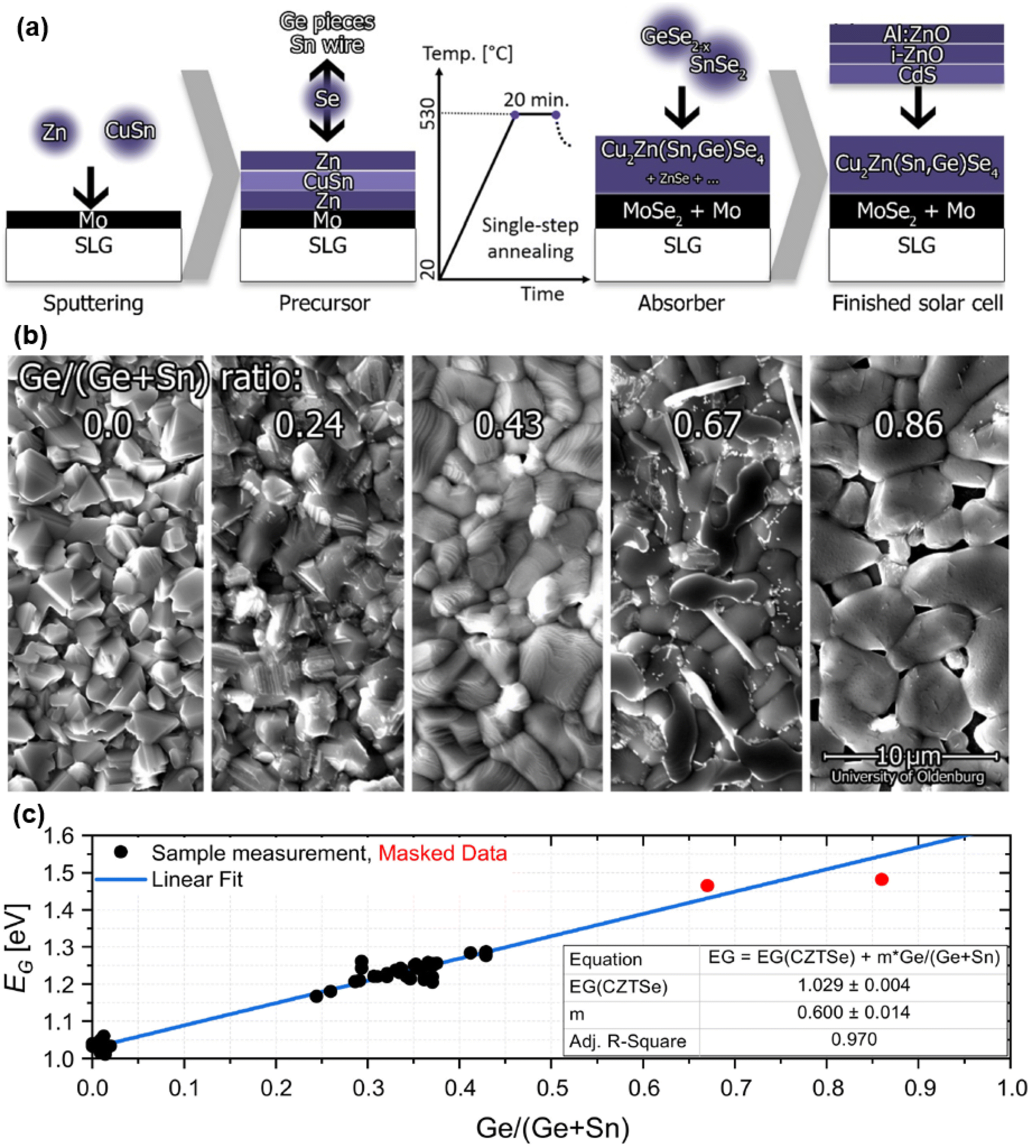
In this work, the focus is placed on the alloying of Ge to partially or completely replace Sn in the CZTSSe kesterite materials, leading to the Cu2ZnSn1−xGex(Sy,Se1−y)4 (CZTGSSe) compounds in which the x = Ge/(Ge + Sn) and y = S/(S + Se) ratios are of particular importance. Theoretically, Ge inclusion is expected to mainly counteract two loss mechanisms greatly affecting kesterite absorbers, namely defect-assisted recombination and band tailing, partly through the replacement of detrimental Sn2+ species.20,24–26 Simultaneously, this strategy should improve PV-related characteristics and allow bandgap tuning,27,28 which is particularly interesting for band alignment optimization. On top of this, experimental studies discussed herein demonstrate that integrating Ge into kesterites also enhances crystalline morphology by mitigating secondary phase formation. These promising advantages of Ge alloying apply to both the bulk and interfaces of the kesterite absorber, as illustrated in Fig. 1(a). At the solar cell level, intensive research effort has provided a steep increase in the PCE of Ge-alloyed kesterites from 6.8% in 2011, the first ever report of a CZTGSSe-based solar cell,29 to around 13% in 2022,30 closing the gap with Ge-free kesterite champion performance. This is depicted in Fig. 1(b).
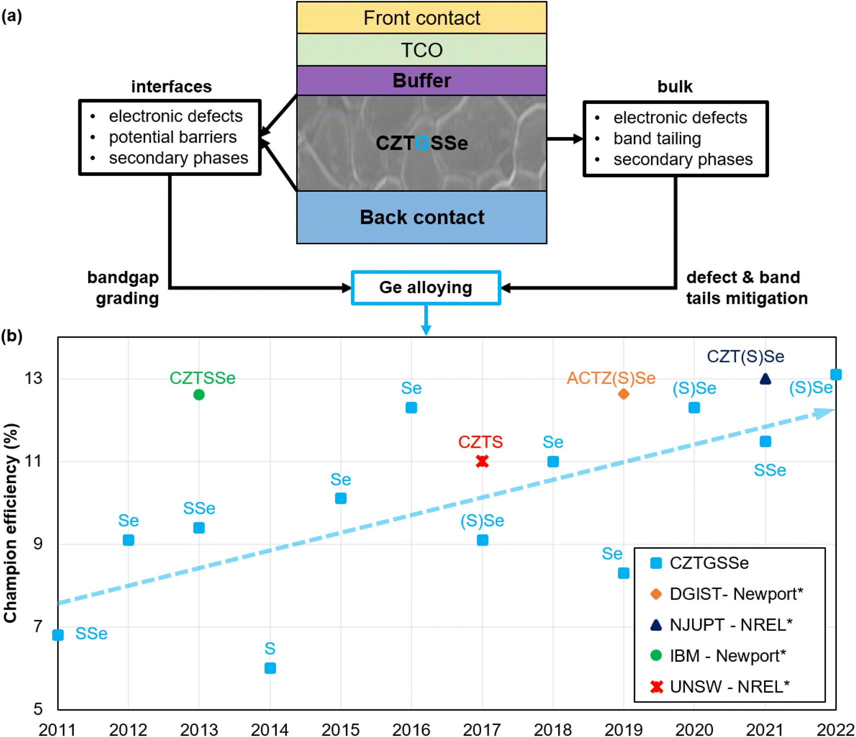 | ||
| Fig. 1 Graphical representation of a generic kesterite solar cell highlighting the main culprits of Voc deficit and the theoretically expected solutions provided by Ge alloying (a). Evolution of the CZTGSSe solar cell champion efficiency reported per year, the trendline of which is depicted by the dashed light blue arrow (b). S and Se respectively stand for sulfur and selenium, put between brackets when present in minute amounts, e.g. (S)Se means Se-rich composition. *Major certified efficiency records of Ge-free kesterites are provided for comparison: the DGIST record has been certified by Newport14,31 (AC in ACTZ(S)Se refers to Ag–Cu alloying in CZTSSe); the NJUPT record is a small-area notable exception measured by NREL;10,32 the IBM record is a notable exception measured by Newport;33,34 the UNSW record is a notable exception measured by NREL.14,35 | ||
From the available literature reports, our work attempts to highlight the most promising Ge inclusion strategy, regarding composition and processing, both in terms of thin-film quality and solar cell performance. Given the undeniable role played by the kesterite absorber and both its surfaces in the solar cell performance, the processing technique and conditions used to deposit CZTGSSe thin films with sufficient quality and suitable PV features are essential, as discussed thoroughly in Section 2. Based on this, their integration in complete solar cells is discussed in Section 3, along with a classification of reported performances with regards to composition. A general summary serves as the conclusion in Section 4, opening up the discussion about future studies needed to push CZTGSSe solar cell performance to higher levels.
2 Thin films
This section aims at gathering most of the findings related to CZTGSSe thin films, both in terms of processing and material properties. On the one hand, we attempt to highlight the respective challenges associated with each processing strategy and the differences between them, not only concerning material quality and the working principle but also more practical aspects. On the other hand, we try to put in evidence the critical requirements for these materials to make suitable absorbers for thin-film solar cells, their dependence on the processing method and conditions and most importantly the incorporation of Ge. The scope of this section is limited to references that (1) rely only on solar cell-compatible deposition techniques and (2) at least include characterization of the CZTGSSe absorber material itself. The results concerning solar cell performance, as well as the references only treating complete CZTGSSe solar cells, are addressed subsequently in Section 3.The first distinction made herein is between vacuum-based and non-vacuum-based thin-film deposition methods. For vacuum-based deposition, another distinction is made to differentiate 1-step from 2-step processes. Then, for each processing approach, the different references are classified according to their x = Ge/(Ge + Sn) and y = S/(S + Se) composition ratios as defined in the Cu2ZnSn1−xGex(Sy,Se1−y)4 formula. This work covers Ge–Sn and S–Se ratios going from 0 to 100% (0 < x ≤ 1 and 0 ≤ y ≤ 1), while pure Sn variations (x = 0) are used as the Ge-free reference case. Apart from x and y, two other stoichiometric ratios are also discussed, namely I/(II + IV) = Cu/(Zn + Sn + Ge) and II/IV = Zn/(Sn + Ge). These determine important kesterite PV properties, and their respective optimal values are widely believed to be Cu-poor (I/(II + IV) ≃ 0.8) and Zn-rich (II/IV ≃ 1.2) for standard CZTSSe,2,12,13,16,19,23 though this is still to be discussed in the following section.
2.1 Vacuum-based deposition
Similar to their chalcogenide counterpart, kesterite thin films are largely produced under vacuum with physical deposition techniques. This is typically achieved by two different approaches: one-step processes, such as co-evaporation, during which all the elements are simultaneously deposited in various high temperature stages leading to the formation of the desired material; two-step or sequential processes consisting in first depositing a stack of metallic precursors usually via sputtering or evaporation, and then annealing at high temperature in a S- and/or Se-containing environment, called the selenization and sulfurization (SAS) step, to obtain the final thin film.CZGSe. CZGSe was first deposited on glass via co-evaporation of Cu, ZnSe, Ge and Se at temperatures from 250 °C to 450 °C to study the impact on the crystalline lattice, surface and bulk morphology, composition and phase as well as the optical bandgap.36 The authors observed that their films contained considerable amounts of Cu while a significant proportion of Ge escaped from the layer especially at higher substrate temperatures. They adapted their processing recipe accordingly and obtained the best results with a 300 °C annealing and 10% less Cu, leading to a single-phase material with p-type conductivity and a bandgap of 1.63 eV.
CZTGSe. Later on, another research group processed CZTGSe thin films by co-evaporation of all pure elements on glass/Mo substrates at temperatures below 250 °C,37–39 greatly inspired from deposition recipes of non-Ge-alloyed kesterites. At the film level, the importance of including GeSe2 within the annealing environment to prevent elemental losses and preserve optimal composition was stressed.37 With an x ratio varying from 0 to 1, the evolution of crystalline phases was presented,37 along with the quasi linear increase (resp. decrease) in the optical bandgap (resp. electron affinity),37–39 in agreement with theoretical predictions.40 It was showed through advanced characterization on similar structures that relatively shallow defects are formed close to the CZTGSe top surface.38 The density of these defects is sufficient to induce a hole-deficiency and compensate for the parallel evolution of bulk states but not high enough to cause Fermi level pinning.38,39 Using similar targets to the first report,36 one group performed co-evaporation of CZTGSe at 150 °C substrate temperature to minimize Sn and Ge loss followed by 330 °C/480 °C two-stage annealing in excess Se to promote grain growth.41 Relying on processing temperatures below 500 °C makes the deposition procedure potentially compatible with flexible polyimide substrates. As an upgrade, they also evaporated a thick Se capping layer before high-temperature annealing to guarantee homogeneity and prevent oxidation.42 With these samples, they revealed the importance of moderate Zn quantity and an appropriate substrate/back contact stack to limit detrimental ZnSe formation while sufficient Na content enhances both carrier concentration and Ge inclusion (Fig. 2). Overall, enhanced grain size was also observed.
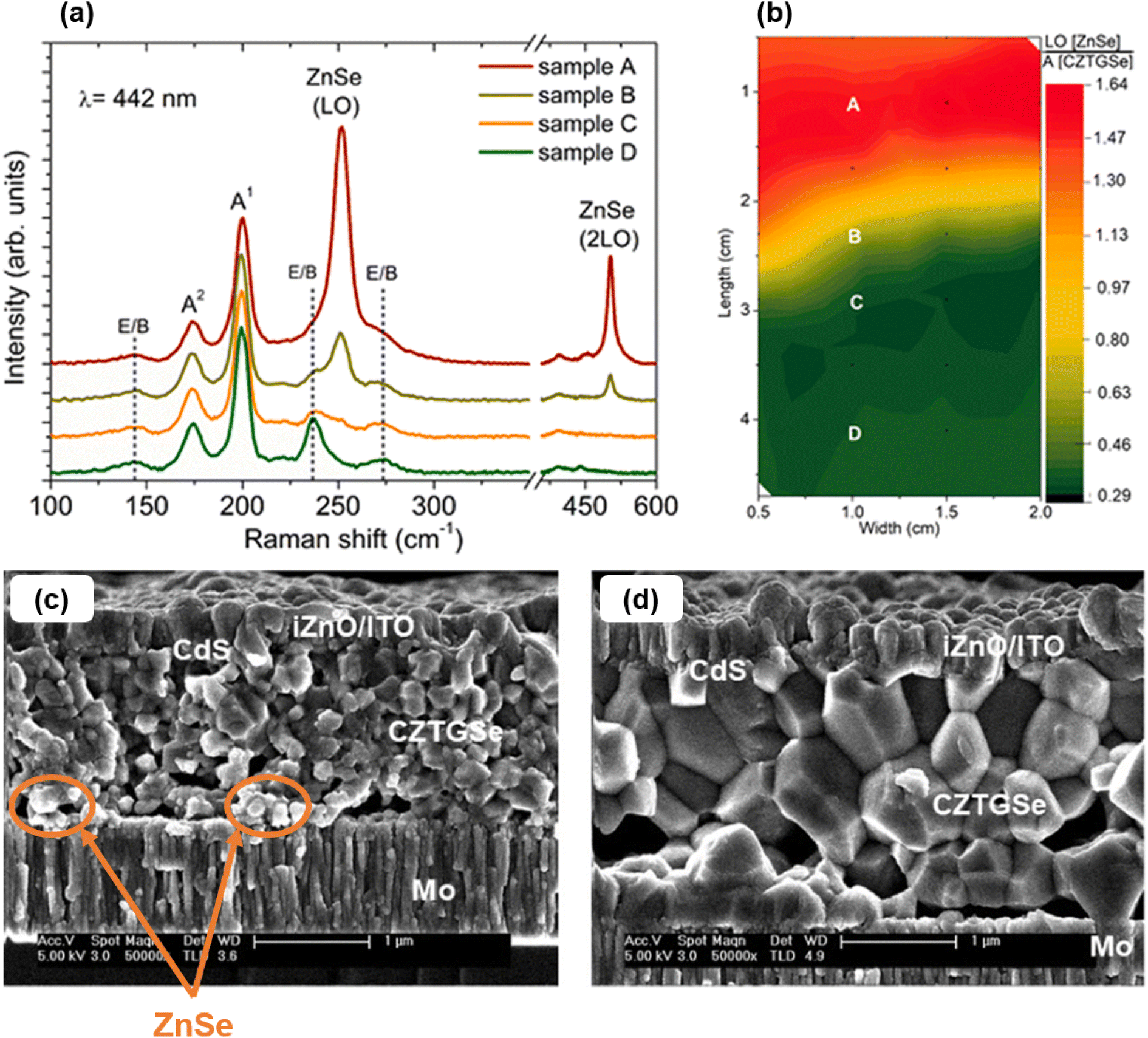 | ||
| Fig. 2 Raman peaks of the compositional sample with varying Zn content (a). Ratio between ZnSe and CZTGSSe Raman peak heights mapped over the compositional sample surface (b). Scanning electron microscopy (SEM) cross sections of complete solar cells including absorbers with sample A (c) and D (d) of the compositional sample, with ZnSe traces highlighted by orange arrows and circles. Adapted with permission.41 Copyright 2020, Elsevier. | ||
CZGSSe. The same team conducted similar experiments on wide-bandgap CZGSSe thin films with and without a Se capping layer.43,44 They highlighted the intricate interplay between the NaF precursor layer, the Se capping layer and S inclusion within the absorber. In general, higher Na quantities promote the integration of more S within the bulk which reduces its surface segregation, and thus smoothens the S-gradient along the absorber thickness and narrows total bandgap grading.
CZTGS. In parallel, CZTGS films were grown via single-stage flash evaporation of a Zn-rich compound with x = 0.5 produced through a modified Bridgman method,45 normally used to produce single crystals. Sn loss was reduced as Ge was successfully integrated into the film at a substrate temperature of 350 °C, which then exhibited good crystallinity and composition even before the subsequent higher-T annealing. Significant dependencies between growth conditions and elemental composition were highlighted, in particular the evolution of Ge, Sn, S and Na during the sulfurization step.
CZGSe. The pioneer investigations about CZGSe thin films relied on simple Cu/Zn/Ge metallic stacks evaporated in a vacuum on both glass and glass/Mo substrates, and then annealed in a Se environment between 400 °C and 500 °C.46 These lead to p-type absorber layers with a micrometer grain size and bandgap around 1.6 eV.
Subsequent studies from another research group enabled to optimize CZGSe thin films processed in a similar way: first, optimizing the Zn precursor thickness, stack ordering, and annealing temperature to prevent the formation of a ZnSe binary phase and enhance the grain size,47 supported by a deep understanding of the crystallization dynamics;48 second, further pushing the elimination of secondary compounds (ZnSe, Ge, GexSey, …) on the absorber top surface by applying chemical treatments based on hot HCl and aqueous (NH4)2S.49 They also revealed the mitigation of deep defect states and band tailing in CZGSe as compared to in standard CZTSe.50 Most of these experiments jointly confirmed an acceptable grain size, single CZGSe phase formation in the 400–500 °C range and suitable p-type doping, conductivity and bandgap for PV applications.
In the continuation of these studies, equivalent experiments were carried out on the same precursor stack, though sputtered and not evaporated, in collaboration with multiple teams of researchers.51–53 In order to improve the absorber crystallinity and mitigate secondary phase formation, the implementation of an optimized selenization recipe with an appropriate surface treatment was investigated.51 The best recipe consisting in a 330 °C/480 °C two-step annealing in Se–GeSe2 led to both high crystalline quality and low Urbach energy,51,52 with only slight traces of ZnSe secondary phases in one study.51 In these two references, KCN etching seems efficient to remove detrimental phases from the top surface with possible non-toxic alternatives based on (NH4)2S combined with KMnO4, but not from the bottom surface where a thin layer with smaller grains is observed. The third investigation consisted in an innovative combinatorial analysis on a sample with graded composition.53 They demonstrated that (1) Cu/(Zn + Ge) = 0.65–0.7 and (2) Zn/Ge = 1.05–1.15 should guarantee CZGSe to be mostly free of secondary phases including those related to Ge, as reported elsewhere.47–52 This seems to be an argument in favour of Ge alloying since for similar Cu-poor and Zn-rich stoichiometry in standard CZTSe, traces of volatile Sn–Se secondary phases can be observed, leading to Sn-loss and defect formation.2,12
Investigations from independent groups attempted to adjust the precursor stack in this two-step process, namely with solid-phase Se integration within the precursor stack,54 or directly evaporating the CZGSe material with the targeted composition.55 Both managed to obtain, for a processing temperature above 450 °C, thin films nearly free of secondary phases and with a similar bandgap to those obtained by the previous groups, but with an overall poorer morphology.
CZGS. Wide bandgap CZGS films exhibited improved morphology and grain size for higher Cu content, as well as a single CZGS phase, whether they are deposited from RF-sputtered Cu, Zn and Ge precursors and then tube furnace sulfurized,56 or from a thermally evaporated binary sulfide precursor and then annealed in a S-containing oven.57 The second group also highlighted the relationship between low Ge content and enhanced crystalline quality, mobility, photoconductivity, as well as reduced defect densities at grain boundaries.57 CZGS thin films were also processed from sputtered CuS/Ge/ZnS precursors on glass/Mo/TiN and then sulfurized, which led to the formation of detrimental secondary phases, ZnS in particular, but also Ge- and Sn-related oxides.58 These oxide phases were successfully etched by KCN surface treatment.
All three groups reported the expected wider bandgap (1.8–2.2 eV) and evolution with regards to composition.56–58 However, as compared to the studies about two-step-processed CZGSe discussed above, these investigations about CZGS showed more evidence of detrimental secondary phases, mainly ZnS, and an overall reduced grain size, potentially explained by the higher volatility of S making grain growth more challenging. Particular attention should be drawn to these aspects to reach a high-quality CZGS material, e.g. for tandem device applications.
CZGSSe. One work reported attempts to process a mixed sulfo-selenide CZGSSe thin film by sequential annealing of a Ge–Zn–Cu precursor stack, first in H2Se at 460 °C and then in H2S at 510 °C.59 Sulfur inclusion from 30 to 100% with an increased bandgap seemed successfully achieved, at the expense of non-uniform composition and degraded morphology. Both the presence of a Zn(S,Se) secondary phase and the lower structural quality observed for a high S content seem in agreement with the differences highlighted just above between CZGSe and CZGS.
CZTGSe. Many references report investigations about CZTGSe absorbers deposited by two-step processes under vacuum, most of them attributed to one research group from IREC and close collaborations,60–70 and a few other investigations carried out by other teams.71–74
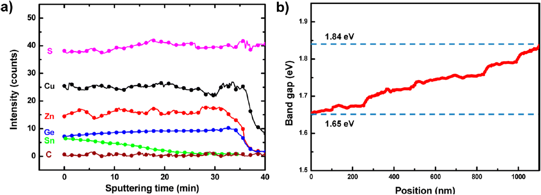
The IREC group implemented and extensively used one approach to process Ge-doped CZTSe, or CZTSe:Ge, thin films on glass/Mo, i.e. sputtering/evaporation of a Cu/Sn/Cu/Zn precursor stack with the addition of a thin thermally evaporated Ge nanolayer at a certain position within the stack, followed by reactive annealing in a Se (and Sn) atmosphere. This recipe is designed to incorporate rather low amounts of Ge, with x ratios typically below 0.1 apart from a few exceptions. The first studies of the series tried to put in evidence an optimum thickness for the superficial Ge layer deposited on top of the metallic stack.60–62 Below 15 nm, they suggested that Ge is barely incorporated within the absorber, apart from GeOx traces visible in Fig. 3(a), explaining the globally unchanged bandgap value as compared to that in Ge-free ref. 62. This is a consequence of the significant Ge loss by the evaporation of volatile GeSe2 during reactive annealing. Still, for that very range of Ge thicknesses, the parallel formation of a Se-rich GexSey liquid phase at 385 °C significantly favours crystallization dynamics,60 as well as Na diffusion.61,62 The consequence is an enhanced grain morphology (Fig. 3(b) and (c)) accompanied by higher doping, less dense grain boundaries and thus, lower defect densities, which are promising for PV applications. However, for thicker Ge precursors, the excess GexSey liquid phase allows discriminated Na atoms to flow towards the surface of the absorber where they oxidize in the form of Na–O needles.61,62 Even though these Na–O particles can be etched by surface treatments, they contribute to lower bulk doping density. For a higher Ge content, delamination near the back contact (Fig. 3(d)) as well as ZnSe and Cu-related secondary phases at the top surface were also observed.60,62
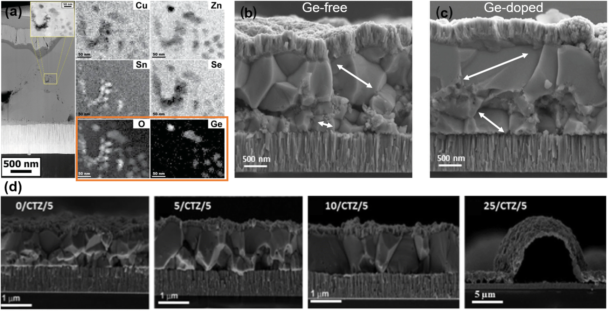 | ||
| Fig. 3 Transmission electron microscopy (TEM)/electron energy loss spectroscopy (EELS) analysis revealing traces of GeOx nanoinclusions highlighted by the orange rectangle (a). SEM cross sections showing grain growth improvement (white arrows) due to Ge doping of the CZTSe absorber (b) and (c). Adapted with permission.60 Copyright 2015, Wiley-VCH. SEM cross sections of CZTSe:Ge absorbers with increasing Ge content, showing delamination issues for the 25 nm Ge bottom layer (d). Adapted from ref. 63 with permission from the Royal Society of Chemistry. | ||
In the continuation of these investigations, they further pushed their understanding of Ge incorporation.63 The main conclusion is that Ge doping allows the kesterite formation mechanism to be fundamentally changed, going from a triple reaction of binary selenides in the Ge-free case to a bi-molecular reaction providing a quaternary phase at an earlier stage in the Ge-doped case. This is due to the Ge inclusion preventing strong elemental segregation, i.e. Cu at the front and Zn/Sn at the back, either by an increased Sn solubility, by a flux-driven crystallization through liquid GexSey, or a combination of both. The consequence is a less abrupt bi-layer morphology (Fig. 3(b) and (c)) with the mitigated presence of a highly volatile SnSe2 phase, thus impeding important Sn loss-related void formation and ensuring higher integrity near the back contact compared to that in pure Sn kesterites. In the same study, they changed the Ge precursor position keeping the total Ge thickness constant between 10 and 15 nm, and demonstrated that the beneficial effect of Ge-doping is not limited to the absorber surface and mainly depends on the total thickness of Ge precursors rather than their position in the stack. Another investigation about CZTSe:Ge layers processed with this recipe provided supplementary insight into the distribution of Ge by using characterization methods with a lower detection threshold.67 Actually, Ge is incorporated over the whole absorber thickness in a heterogeneous fashion, creating Ge-rich and Ge-deficient zones within the grains and at their boundaries, under the form of previously observed GeO2 inclusions and possible secondary phases. As complementary studies, this research group investigated alternatives to sputtering for depositing the precursor stack, such as thermal evaporation,69 or molecular beam epitaxy.64 The former lead to mostly identical results compared to sputtered precursors apart from the remarkable absence of Sn–Se secondary phases, whereas the latter still requires further optimization in the control of elemental diffusion, composition and processing parameters.
Similar experiments performed in parallel within the same team focused on pre-selenized nanocrystalline CZTSe precursors65,66 doped with Ge and annealed using the usual IREC approach. These studies demonstrate that x values below 2 to 4% (1) induce low Ge incorporation evidenced by the nearly constant bandgap values, (2) restrict the formation of both bulk defects (Fig. 4(a)–(c)) and chemically etchable surface secondary phases and (3) enhance carrier density through Na interaction (Fig. 4(d) and (e)), while inverse trends are observed for a higher Ge content.65,66 All these conclusions coincide with the standard IREC processing results.60–62 However, in this case, Ge doping does not allow further grain size improvements compared to those already induced by pre-selenization,65,66 and apparently has no influence on band tailing.66
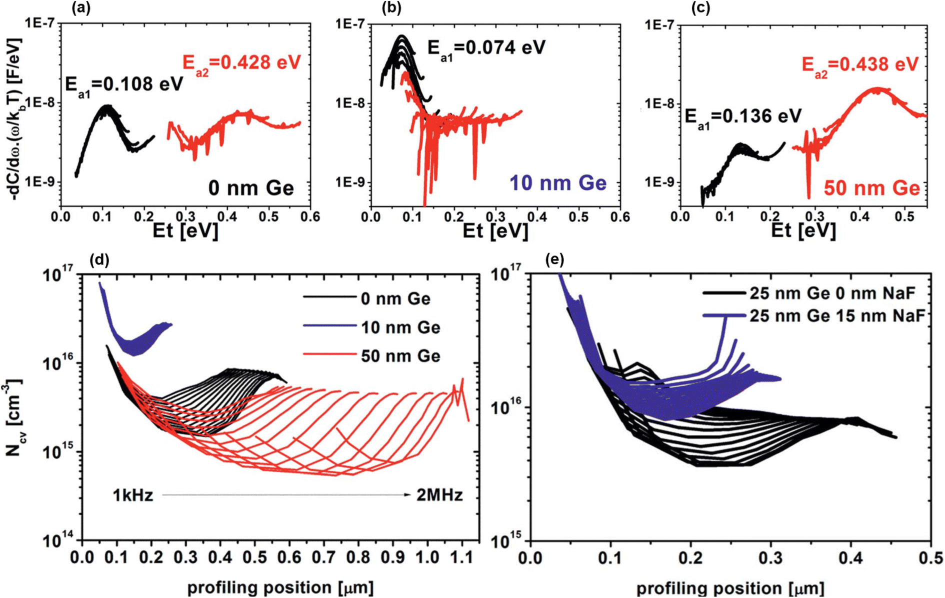 | ||
| Fig. 4 Bulk defect energy profile with a Ge nanolayer of 0 nm (a), 10 nm (b) and 50 nm (c). Capacitance–voltage-derived doping profile for various Ge nanolayer thicknesses without a NaF layer (d) and fixed 25 nm Ge with and without a NaF layer (e). Adapted with permission.66 Copyright 2018, RSC. | ||
Another important aspect of Ge-alloying is the possibility to perform bandgap grading without relying on the S/(S + Se) ratio, equivalently to the Ga/(Ga + In) ratio in CIGSe-based devices.9 Since the references discussed above reported little influence of Ge doping on the bandgap value, Sn–Ge bandgap grading was studied for higher Ge content in two different studies.68,70 They described a natural Sn–Ge segregation appearing in CZTGSe thin films as resulting from the reaction of GeSe with CZTSe near the back contact, subsequently leading to the formation of CZTGSe and SnSe2 in the same region. These findings are well in agreement with the CZTSe/CZTGSe bi-layer morphology reported before,60,63,65 and happens concomitantly to the diffusion of Na, Cu and Ge precipitates towards the bottom surface where MoSe2 is also detected.70 The observed irregular compositions along the absorber thickness could support the formation of secondary phases. As a direct consequence of the graded Sn–Ge ratio, natural bandgap grading was demonstrated in these absorbers,68,70 sometimes with a steep profile fashion going from x = 0.8 at the back to x = 0.1 at the front and mainly controlled by the annealing conditions.70 As the global Ge content increases above x = 0.2, a trade-off appears between the mitigated void formation due to SnSe2 evaporation and the reduced grain size.
Another work presented a Sn–Ge gradient for CZTGSe absorbers grown from different variations of the same metallic precursor stack, leading to shallow bandgap grading towards the back.71 Besides that, one study reproduced similar improvements related to Ge doping as those brought by the IREC Ge nanolayer approach,74 namely an increased doping concentration and enhanced morphology. This improved structural quality was jointly observed by two different teams investigating an alternative strategy that consists in integrating Ge only during the selenization step of a sputtered stack, either in a GeSe2–Se,72 or a pure Se–Sn–Ge environment73 as shown in Fig. 5(a). The former focused on Ge doping (x < 0.02) and highlighted the widely seen bi-layered absorber with a Ge gradient towards the back promoting alkali diffusion, no secondary phases and reduced band tails.72 The latter discovered two dependencies on the value of x ranging from 0 to 1:73 first, an enlarging spread of the Sn–Se binary phase in both the bulk and at the surface, the evaporation of which may likely explain the voids observed in between the Ge-enlarged grains (Fig. 5(b)). Second, a linearly increasing bandgap value (Fig. 5(c)) in parallel with a more pronounced band tailing. Besides that, they also concluded that Ge integrates into the film at temperatures above 400 °C, thus not interfering with the kesterite phase formation but only its transition from Cu-rich to Cu-poor stoichiometry.
 | ||
| Fig. 5 Graphical workflow of the CZTGSe absorber and solar cell processing based on vapor-phase incorporation of Ge (a). SEM pictures showing evolution of the surface morphology as a function of the Ge content (b). Evolution of the bandgap extracted from external quantum efficiency (EQE) measurements (c), as a function of the x = Ge/(Ge + Sn) ratio, following the linear relationship: Eg(x) = 1.03 + 0.6x. Adapted with permission.73 Copyright 2022, MDPI. | ||
CZTGS. Four different methods are investigated and optimized to deposit high-quality CZTGS films on glass/Mo through tube furnace sulfurization of a precursor stack. First, a sputtered Zn/Cu/Ge/Sn stack is sulfurized in sulfur vapour, covering x ratios from 0 to 1 by changing the thicknesses of the Ge and Sn layers.75 When the x ratio increases from 0 to around 0.7, grains become bigger whereas the absorber surface gets rougher. For even higher Ge content, the inverse trend is observed, along with void formation near the back contact which is attributed to Ge sulfide escape, as similarly highlighted for CZTGSe.68 Second,76 the co-sputtering of a pioneering CZGS/CZTS bi-layer precursor sulfurized at high temperature was more recently investigated. This enabled bandgap-engineered CZTGS films with a Sn–Ge gradient along the absorber thickness to be obtained possibly creating a beneficial back surface field, similarly to the Ga gradient in CIGSe devices.9 The counterpart of this graded morphology is a bi-layered structure constituted of (1) large and compact Sn-rich grains in the upper half of the absorber and (2) small Ge-rich grains accumulated at the back with GeOx phases, cracks and voids observed at their boundaries. This bottom layer with a higher Ge content and poorer morphology suffers from the same delamination issues reported in other studies related to Ge–(S,Se) escape.62,63,68,70,75 Later on, the same group successfully tackled these adhesion issues related to the Ge-rich bottom layer by using a TiN interlayer between the Mo electrode and the CZTGS absorber.77 Third, the evaporation of 20 nm Ge followed by the sputtering of a stacked Cu/SnS/Zn precursor with varying Zn thickness was performed before sulfurization.78 As also demonstrated for one-step-processed CZTGSe,41,42 a lower Zn content tends to restrain the spreading of ZnS phases which tend to concentrate near the back contact. If one further reduces the amount of Zn to reach Zn-poor compositions, high density of deep SnZn defects would be expected, but the substitution of Sn with Ge probably helps in preventing their detrimental activity as compared to standard CZTS.78 One conclusion of this study is that a slight Zn-deficient stoichiometry may be more ideal for CZTGS than the widely accepted Zn-rich optimal composition for CZTS. Fourth, the last research group studied the addition of a Ge nanolayer of different thicknesses at different positions in a sputtered Cu/Sn/Cu/Zn stack.79 5 nm Ge on top of the precursor stack seemed to provide the most efficient Ge incorporation into the Ge-doped CZTS (or CZTS:Ge) absorber. They revealed that such small amounts of Ge have no significant impact on morphology but are sufficient to mitigate, though not totally eliminate, SnS2 secondary phases which are commonly observed in pure Sn kesterites.
Several observations were common to the CZTGS references discussed here. First, ZnS was detected in nearly all studies,75–78 agglomerating at grain boundaries or both the top and bottom surfaces of the absorber, where it limits grain size. Second, they all reported the appearance of a layer with poorer morphology near the back contact,75–79 exhibiting void creation and back surface delamination through the escape of Ge sulfides,75 the formation of Ge oxides,76,77 and the segregation of a ZnS phase,78 or a combination of these effects. Third, joint evidence of enhanced grain size for moderate Ge incorporation is reported.75–78 Fourth, bandgap values between 1.4 and 1.5 eV were obtained for low amounts of Ge,76,78,79 reaching up to 2.23 eV for x = 1.76 Overall, the advantages of Ge inclusion in CZTS tend to be less obvious compared to those for the Se-based equivalent, potentially explained by the absence of liquid phase-assisted crystallization in the S-based compounds.56,61–63,79
CZTGSSe. Two studies investigated the addition of a thin sputtered Ge layer either below and/or above the Mo back contact of CZTSSe absorbers on flexible Ti.80,81 In these structures, the CZTSSe absorber is co-sputtered in a Zn + CZTS/Cu + CZTS/Zn + CZTS 3-layer approach and then selenized. On the whole, inserting Ge below the Mo back contact tends to significantly improve adhesion and limit residual stress, which are important aspects for flexible devices. Similar to Ge-doped CZTSe and CZTS discussed above, a thin Ge nanolayer below the CZTSSe absorber induces greater crystallinity and bigger grains with a nearly unchanged bandgap and no undesired phases, but the cost is a rougher surface. All these observations tend to be correlated with the substitution of Sn with Ge that promotes Sn4+ over Sn2+ species, a well-known defect-prone issue in kesterites,20 which needs to be mitigated for enhanced efficiency.82
Sputtering CZTG precursor stacks followed by rapid thermal annealing in a Se-rich (S,Se) atmosphere was used to deposit CZTGSSe films over glass/Mo substrates in two different studies.83,84 For Ge-doping with x < 0.2, evidence was found of single-phase CZTGSSe kesterite without bulk secondary phases, increased grain size and reduced IV-loss leading to mitigated void formation, compared to pure Sn CZTSSe. Fine control of the Ge nanolayer thickness and position allows proper stoichiometry to be preserved and both morphology and crystallinity to be enhanced. Similar findings were obtained with a single-target sputtering of CZTS before GeSe2–Se annealing.85 The main differences are, as compared to the two previous studies,83,84 a homogeneous morphology over the whole thickness potentially supported by the use of GeSe2 annealing and the presence of a ZnSe phase likely due to the high Zn content. Finally, another processing strategy was used,86 relying on CZTGS single-target pulsed laser deposition (PLD) with varying selenization conditions. To our knowledge, it is the only report of a Ge-alloyed kesterite absorber processed via PLD, considered to be easily controllable with regards to film composition.86 As most references up to this point, they found that Ge incorporation tends to improve the structural quality of the layer. On top of this, optimizing the selenization process in terms of the Se content, duration and temperature revealed that all three parameters simultaneously influence the crystallinity, phase formation, grain size, composition and bandgap, with an optimal recipe of 45 mg Se for 10 min at 550 °C.
Nanopowders. Several experiments were also carried out on Ge-containing kesterite polycrystalline powders.87–89 Even though not concerning actual thin films, these respectively reveal the dominance of defect-assisted recombination for x < 0.2 and of valence band tail-assisted recombination for x > 0.2 in CZTGSe;87 alternative Cu-related point defects in Cu-rich CZGSe;88 the challenge to process single-phase CZGSSe.89
2.2 Non-vacuum-based deposition
Contrary to their CIGSe cousin, it is not yet clear for kesterite PV absorbers, including Ge-alloyed ones, whether physical vacuum-based or chemical non-vacuum-based depositions provide higher material quality and device performance. Indeed, there are nearly as many investigations reported on these admittedly more simple and low-cost solution-based methods than on those relying on in-vacuum steps. Non-vacuum processes have a similar sequence to the two-step vacuum-based techniques discussed above. The main difference is the precursor deposition step, typically realized in ambient solution with a much wider panel of deposition methods and resulting in a non-layered thin-film precursor yet to be annealed. Consequently, the relevant deposition parameters and possible recipe modifications greatly differ from those of two-step vacuum processing, with for instance the importance of choosing the appropriate solvent or adding adapted catalysts. The reported investigations are discussed below, at the absorber material level.An alternative precursor processing based on binary sulfide paste doctor blade deposition was investigated for CZGS,91 targeting a Cu-poor stoichiometry. They concluded that a suitable post-sulfurization temperature and duration would be 500 °C for around 30 min to guarantee much-improved crystallinity and no secondary phases compared to the as-deposited film, similarly to ref. 90. In both references, films with similar I/II + IV and II/IV ratios exhibit a similar micron-wide grain size and bandgap values. This is quite well adapted to PV applications, along with the processing solutions used that are theoretically compatible with large-area production.
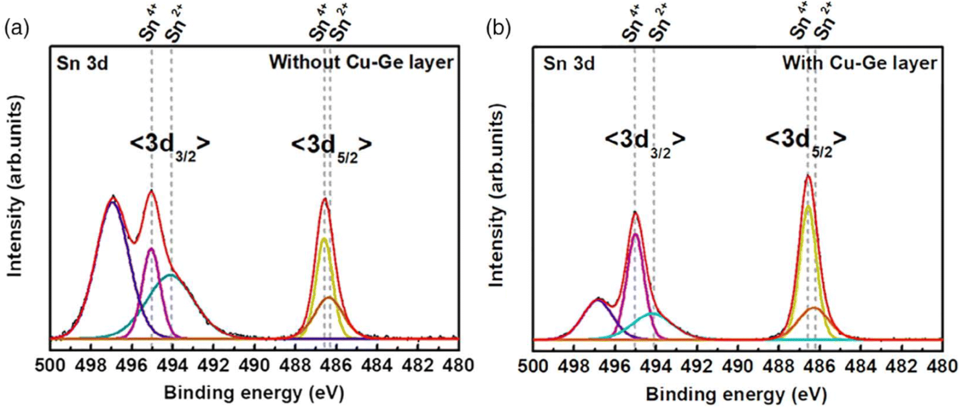 | ||
| Fig. 6 X-ray photoelectron spectroscopy (XPS) results showing the reduction of Sn2+ species when going from no Cu–Ge layer (a) to a Cu–Ge bottom nanolayer (b), in the kesterite absorber processing via electrodeposition. Adapted with permission.95 Copyright 2020, Wiley-VCH. | ||
Similar trends were reported for two alternative methods to process the precursors before annealing. On the one hand, a Ge nanolayer is vacuum-sputtered below the solution coated CZTS film,101 leading to more compact and large-grain CZTS:Ge layers after sulfurization. On the other hand, a chloride-based CZTG precursor solution of varying x ratios is spin-coated and annealed in H2S![[thin space (1/6-em)]](https://www.rsc.org/images/entities/char_2009.gif) :Ar at various flow rates.102
:Ar at various flow rates.102
As observed for vacuum-processing, the improvements related to Ge inclusion are more striking for CZTGSe than for CZTGS in solution-based methods also, especially the enhanced grain growth and film morphology. Since these two aspects are closely related to the annealing process, it sounds plausible to explain the higher effectiveness of Ge inclusion in improving CZTGSe absorbers by liquid-phase assisted crystallization,56,61–63,79 as for the two-step vacuum processes above.
The pioneer work of Ge-alloyed kesterite solar cells relied on CZTGS nanocrystals processed through hot injection (batch reaction) in oleylamine, and then doctor blade coated on glass/Mo and selenized at 500–550 °C to form the final CZTGSSe thin film.29,103,104 Three observations were jointly reported: (1) bi-layer morphology with Ge-integrated large crystalline grains along the upper half and small Se- and carbon-rich grains towards the back contact, (2) tunable bandgap above 1.09 eV for increasing Ge content and (3) group IV elemental loss due to the evaporation of Sn or Ge sulfides and selenides during annealing. The last phenomenon should be avoided, which was tackled successfully within the bulk but not at the surface using different Ge precursors.104 Similar trends regarding the bandgap and Sn–Ge loss were highlighted in two other studies also relying on a nanocrystal-based deposition route,105,106 with a few supplementary findings. First, within the same group, chloride salt-based molecular ink spray-coating of precursors before selenization allowed to demonstrate that the Ge loss is greater than that for Sn in CZTGSSe thin films.106 Second, in another research team, an air-stable GeO2-based processing recipe mixing CZGS and CZTS inks led to crystalline films with increased grain size for low to moderate Ge incorporation.105
Besides that, various solvents and Ge sources were employed in the solution spin-coating-based precursor deposition before SAS: polymer-assisted aqueous solution including GeO2,107 non-toxic butylamine-based solution including GeSe2,108 Ge-free dimethyl-sulfoxide solution,109,110 organic solvent-stabilized precursor solution including either GeO2 (ref. 111) or an evaporated Ge bottom nanolayer,112 water- and metallic oxide-based solution,113 a GeO2 precursor layer below a CZTSSe precursor30 (Fig. 7(a)), and Ge-containing chlorine-based solution drop cast during annealing.114 In all these references, effective Ge inclusion is reported (Fig. 7(b)), by substitution onto Sn sites and/or under the form of oxides. This arguably led to globally increased grain size for higher Ge content, in turn improving the large-grain/fine-grain ratio of the typical bi-layer morphology usually observed,30,107,108,111–113 except for one group that integrated Ge only at the annealing step and for which liquid-phase assisted crystallization may have allowed a uniform structure.109,110 The importance of fine composition tuning is closely related, and is once again stressed to prevent the appearance of (1) detrimental secondary phases such as Zn(S,Se) and CuxSe109,110,113 or (2) voids and cracks through excess Ge sulfide and selenide sublimation.30,105,108 Apart from the usually demonstrated tunable bandgap,107,113 other opto-electronic properties such as doping concentration,30,107,113 mobility,107,113 and resistivity107,113 can be controlled by the amount of Ge incorporated, and globally enhanced for x < 0.4. Eventually, Ge alloying exhibited strong abilities to mitigate both defect-assisted recombination and band tailing30,109–112 (Fig. 7(c) and (d)), likely by the neutralization of well-known SnZn and CuZn “killer” defects due to the lowering of the undesired Sn2+ species concentration.30,112
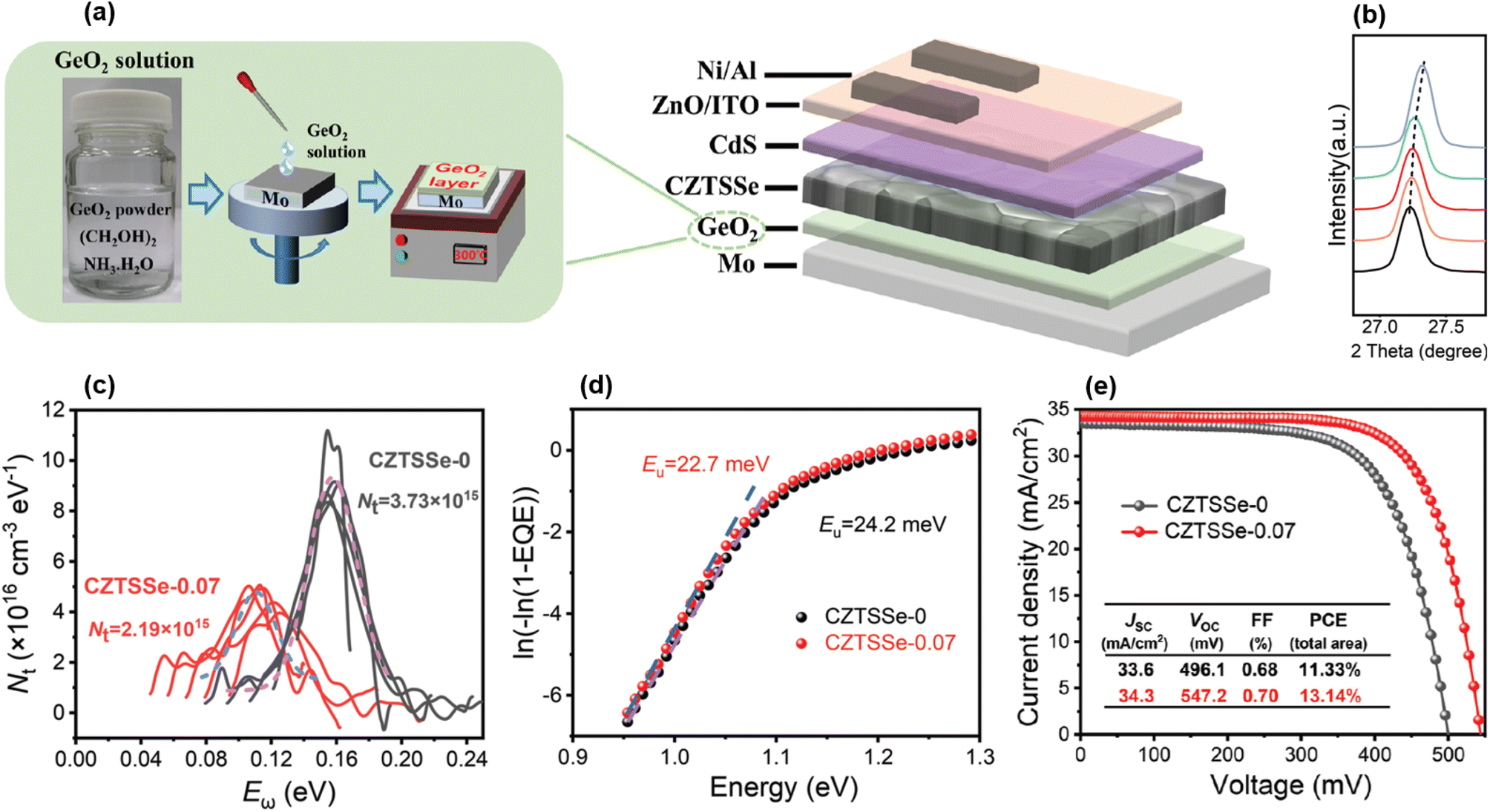 | ||
| Fig. 7 Graphical representation of the processing setup (a). X-ray diffraction spectroscopy (XRD) results proving the proper inclusion of Ge within the kesterite crystalline lattice, for varying the x ratio (b). Opto-electrical characterization showing reduced bulk defect density (c) and Urbach energy (d). Current–voltage (I–V) curves under AM1.5G illumination exhibiting 13.14% PCE for Ge-doped kesterite (e). Adapted with permission.30 Copyright 2022, Wiley-VCH. | ||
2.3 Discussion
• Overall, Ge can be properly incorporated into the kesterite crystalline lattice onto Sn sites. Still, it may also be detected in the form of GeOx nanoinclusions at grain boundaries, possibly acting as passivation elements (electron back reflectors), in excess at surfaces or within secondary phases. All these Ge phases are not always uniformly distributed, with a global concentration near the back contact following the natural Ge down-diffusion, but also segregated between grain interiors and boundaries.
• Compared to Ge-free kesterites, the most obvious improvement related to Ge alloying is morphological. First, an enlarged grain size close to or beyond the micron scale is nearly always reported, depending on the amount of Ge, sometimes at the expense of a rougher surface. Second, the typical bi-layer kesterite morphology is partly resolved with a more prominent large-grain top layer than the fine-grain bottom layer. Third, void formation due to the evaporation of group IV-(S,Se)2 compounds near the back contact is mitigated given their lower volatility in the case of Ge, thus diminishing chances of delamination and shunting. These observations are especially verified in the case of Se-rich kesterites, for which the explanation seems to reside in a modified reaction mechanism.60–63,65–68 Indeed, Ge tends to integrate the kesterite phase at a lower temperature than Sn which lessens elemental segregation between the back and front, namely through GexSey liquid-phase assisted flux-crystallization. This in turn supports grain growth and facilitates the diffusion of metal and alkali elements, leading to a higher structural integrity and thin-film quality.
• This Ge-boosted morphology along with kesterite phase purity is attainable as long as the appropriate composition and Ge concentration are ensured. For standard kesterites, Zn-rich (II/IV 1.2) and Cu-poor (I/(II + IV) 0.8) ranges are widely recognized as optimums with respect to solar cell performance. Equivalent values are also found in the particular case of Ge alloying, with slight refinements claimed in certain studies. Respecting such compositions allows the mitigation of the spreading of undesired binary phases that are detrimental to solar cell performance, e.g. Cux(S,Se), IV-(S,Se), IV-(S,Se)2, and elemental Ge or Zn(S,Se). This last compound is mostly eliminated in a Zn-rich stoichiometry but still largely observed and particularly disadvantageous through increased leakage and/or a reduced grain size. Since Ge tends to greatly modify the reaction mechanism during kesterite formation, the final composition is quite dependent on the Ge proportion itself. In that regard, most reports highlight the importance of non-excessive Ge content (roughly x < 0.4) to guarantee large-grain, dense and non-porous absorber layers without voids, surface impurities and detrimental secondary phases. Even the slightest composition change may have a great impact on the final thin film. Thus, accurate control of the stoichiometry is key to minimize large variations between the different processing stages, for instance by compensating elemental loss during the annealing step, and guaranteeing absorber homogeneity.
• The elemental composition also has a great influence on the opto-electronic properties of the kesterite materials. First and foremost, it is possible to finely tune the bandgap of Cu2ZnSn1−xGex(Sy,Se1−y)4 absorbers through x instead of y, which is advantageous as mentioned in Section 1. Moreover, the bandgap itself tends to be naturally graded towards the back following the Sn–Ge segregation occurring during the annealing step. This should allow interface recombination to be counteracted through bandgap engineering at the solar cell level. Second, Ge alloying also enables a reduction of both bulk recombination and band tailing through the mitigation of, respectively, highly detrimental deep defects such as CuSn or SnZn donor states complexed with CuZn into [2CuZn + –SnZn], and Cu–Zn disorder [CuZn + ZnCu]. This is likely related to the effective substitution of bivalent Sn2+ and Sn4+ by monovalent Ge4+ species. Finally, incorporating appropriate amounts of Ge into CZTGSSe absorbers also globally enhances essential parameters such as the carrier lifetime, mobility and carrier concentration among others. Physically, the two former parameters seem rather related to the improved morphology whereas the latter is partly explained by the creation of CuGe and VGe acceptors as well as the demonstrated interaction between Ge and Na through the liquid Ge–Se phase.
The first noticeable difference between processing strategies is the higher quality and integrity of CZTGSSe thin films processed in a vacuum in one-step,36,37,41 as compared to two-step recipes.47,48,57,59,62,63,68,70,73,75,76 For the former, secondary phase mitigation appears relatively straightforward while the latter globally demonstrates poorer adhesion and morphology, respectively, explained to a certain extent by the escape of Ge or Sn sulfides and selenides59,68,75,76 and grain growth-limiting Zn(S,Se) phases.48,54,56,57,59,75 The second and even more remarkable difference is the nearly complete absence of secondary phases for solution-based deposition techniques, which thus globally provide kesterite films with higher crystallinity than vacuum-based physical processing. One could have expected the inverse as in the case of CIGSe, given that vacuum should typically reduce the risks of external contamination or elemental losses, among others. Different hypotheses could explain this peculiar observation. First, an accurate and reproducible control of the stoichiometry seems equally feasible, if not more, by monitoring the diluted quantities in a solution than by physically depositing stacked layers of expected thicknesses as performed in sequential vacuum-based recipes. Second, the importance of elemental dynamics and the physical state in the growth of kesterite compounds has been largely put in evidence for sequential vacuum processes, namely leading to back surface delamination and void formation.47,48,54,57,59,62,63,67,68,70,73,75,76 In contrast, this is much less observed for Ge-alloyed kesterites processed in ambient solution,94,108,114 with adapted solutions to be implemented already at the precursor level.107 Third, mixing sulfur and selenium is particularly challenging to be realized in the gas phase,37 given the much higher volatility of the former, which may be resolved more easily when already integrated at the precursor level in the liquid or solid phase as for solution-based processing.
From the above discussion, one could conclude that non-vacuum-based methods are the optimal approach for processing CZTGSSe thin-film absorbers. Indeed, it globally enables equivalent absorber quality as vacuum-based deposition with a more accurate composition tuning and less secondary phases, while relying on less complex and more affordable experimental setups. However, they presently have a lower up-scaling potential than industrially established vacuum-based techniques such as (co-)evaporation or sputtering for instance, which remains an essential aspect in the wide spreading of PV technologies. Moreover, the performance of the resulting solar cells remains a major decision criterion and should then be discussed before taking any conclusion, as done below.
3 Solar cells
In this section, the performance of CZTGSSe solar cells is detailed with, to our knowledge, nearly all reported efficiencies up to the time of writing. The primary figures-of-merit used to gauge solar cell performance typically are the efficiency (η) in %, the open-circuit voltage (Voc) in mV, the short-circuit current density (Jsc) in mA cm−2, and the fill factor (FF) in %. To take into account the variations of Voc, Jsc and FF that are not only bandgap-related and putting them in parallel with the theoretical limits famously established by Shockley–Queisser (SQ),121 we here consider instead the SQ deficits defined as VocSQ,def = VSQoc − Voc, JscSQ,def = JSQsc − Jsc and FFSQdef = FFSQ − FF using the same units. These are fixed for a certain bandgap, either taken from the reference itself or deducted from the composition following Eg(x) = x × Eg,CZGSSe + (1 − x) × Eg,CZTSSe − b × x × (1 − x) with b = 0.1 eV (ref. 27 and 97–100) when not applicable. To do so, we use the tabulated values of VocSQ, JscSQ and FFSQ for the AM1.5G solar spectrum,122 from which we subtract the reported values of Voc, Jsc and FF. These deficit metrics are displayed as a function of both the x = Ge/(Ge + Sn) ratio and the y = S/(S + Se) ratio on “compositional maps” (Fig. 8 and as a list in Table S1†), and separated in four different groups thoroughly used to establish the physical reasoning below. Other aspects that are specific to complete solar cells are also addressed, e.g. buffer material, diode parameters (ideality factor n and saturation current J0), electrical parasitics (shunt resistance Rsh and series resistance Rs), or interface optimization.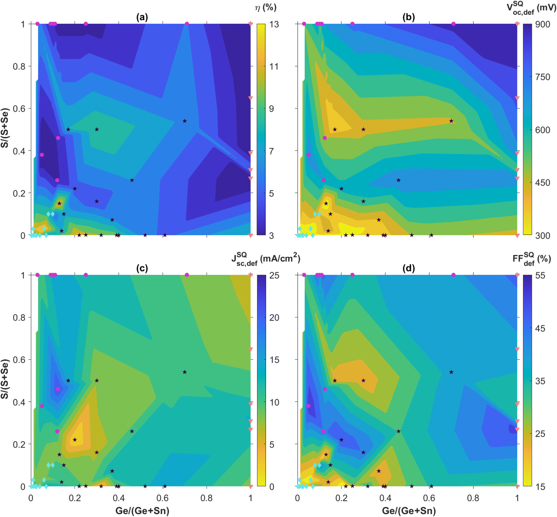 | ||
| Fig. 8 Reported champion solar cell efficiency η (a), and extracted SQ deficits VocSQ,def, JscSQ,def, and FFSQdef (b) to (d), expressed as a function of the composition ratios x = Ge/(Ge + Sn) and y = S/(S + Se) as reported in the references reviewed. The highest efficiencies and lowest deficits are highlighted in yellow. The color levels are equally spaced between the minimum and maximum values for each map and chosen in a sufficient number to ensure clarity. Data points are separated in 4 different groups corresponding to the subsections herein: group 1 (Ge-doping and Se-rich) in light blue diamonds, group 2 (Ge-doping and S-rich) in purple circles, group 3 (Ge-moderate and Se-rich) in black stars and group 4 (Pure-Ge) in orange triangles. The narrow white area along the left edge of the maps corresponds to lacking reports. Solar cell figures-of-merit beyond the SQ limits are left out of the compositional maps but their (x,y) composition pair is still displayed for statistical relevance. The corresponding data are provided in Table S1†. | ||
3.1 Ge-doping and Se-rich
The first remarkable feature on the efficiency map appears in the bottom left corner, i.e. the low-Ge and Se-rich region for x < 0.1 and y < 0.1, designated as group 1 and shown as light blue diamonds in Fig. 8(a). By not only concentrating a large amount of references relying on either sequential physical or solution-based processing, this composition area includes a significant part of the highest reported efficiencies from 8% up to 13%, with low SQ deficits around 300 mV, 10 mA cm−2 and 15% for Voc, Jsc and FF, respectively. Within the numerous studies related to these CZTSe:Ge absorbers, hypotheses explaining this “sweet spot” for efficiency can be found, more particularly through the low SQ deficits accounting for Voc and FF (Fig. 8). Using their pioneer Ge nanolayer approach, IREC highlighted that Ge doping onto Sn sites does not either significantly affect the bandgap value or solve the widely recognized Voc-detrimental band tailing effect.66 Still, they revealed that Ge doping seems promising to counteract two other important culprits for a Voc deficit,60–63,65–67i.e. large defect concentration and low net doping, recently put in evidence as the main limiting factors towards high performance.17 On the one hand, high-density deep bulk defects are partially neutralized, likely as a consequence of Sn2+ species mitigation, thus reducing recombination as suggested by the lower n and J0 values reported. On the other hand, carrier density is increased following the interaction between Ge and Na that is boosted by the IREC-discovered “liquid phase-assisted flux crystallization” mechanism in CZTSe:Ge. Another essential outcome of this novel reaction pathway is a greatly improved morphology, i.e. more uniform, void-free and grain-enhanced, that likely justifies the enhanced FF values, usually via higher shunt resistances. All these observations typically stand as long as the x ratio is kept low,60–63,65–67 revealing the importance of fine composition tuning. Following this wholesome study about the absorber quality, IREC pushed the optimization further with back and front contact characterization.123,124 They proposed that limited Ge quantities help in reducing the detrimental Mo/MoSe2 back contact barrier height and the associated series resistance through a reduced defect concentration, possibly also contributing to the low Voc and FF deficits as observed elsewhere.30Other groups reported similar observations,30,72,83,95,96,109,112 sometimes with even higher solar cell performance possibly explained to some extent by the alternative Ge doping or absorber deposition approaches used, i.e. either solution-based30,95,96,112 and/or relying on Ge-atmosphere annealing72,109 which respectively mitigate secondary phase formation and Ge-loss,104 as discussed in Section 2. It is quite remarkable to note that the natural Sn–Ge segregation appearing in these materials may be either an asset or a disadvantage. In one case, it is used as a way to create shallow back bandgap grading,71,72 acting together with grain boundary potential barriers to improve carrier separation via limited rear interface recombination.72 In another case, it is resolved via a Cu–Ge bottom layer and arguably linked to deep defect neutralization and band structure enhancement.95 The fact that these two antinomial approaches both lead to large Voc and FF gains stresses the difficulty to design efficient kesterite solar cells and the need for further investigations. Besides that, slightly relieved band tails were also observed after Ge doping.30,72,109 Tackling most of the loss mechanisms discussed herein led to the all-time record efficiency of 13.1% for Ge-alloyed kesterite solar cells,30 based on a CZTSSe absorber deposited on a GeO2 bottom nanolayer, both solution-processed (Fig. 7(e)).
3.2 Ge-doping and S-rich
For similar small amounts of Ge, S-rich compounds have been less investigated and the reports available exhibit much lower performance than Se-rich kesterites, gathered in group 2 and shown as purple circles in Fig. 8. With a vast majority of physical sequential processing,77–81 only one group followed the solution-based route to obtain similar performance with a higher Voc but a poorer Jsc and FF.101 The explanation for the poor efficiencies observed in group 2 in Fig. 8(a) seems two-fold: first, S-rich stoichiometry for kesterite solar cells generally induces higher Voc deficit than the Se-rich alternative,18,125,126 whether it is for record standard Ge-free cells14 or Ge-alloyed kesterites reviewed herein (Fig. 8(b)); second and more importantly, the morphology improvements induced by Ge doping tend to be less significant for S-containing kesterite materials, likely due to the absence of a GeSe fluxing agent during thin-film growth (Section 2) that could explain the striking differences in the FFSQdef between group 1 and 2 as shown in Fig. 8(d).Moving away from this low-Ge and high-S composition range was investigated in four different studies (purple circles far from the top left corner in Fig. 8), but did not lead to a clear reduction of the SQ deficits. On the side of the chalcogen ratio, reducing the S content for Ge-doped kesterites towards a S–Se mixed stoichiometry was attempted on flexible substrates80,81 or by pulsed laser deposition,86 both with efficiencies not exceeding 4%. On the side of the group IV ratio, going beyond the 40% Ge limit previously established in Section 2 to realize bandgap grading in CZTGS (Fig. 9) reached not more than 6% PCE.100
 | ||
| Fig. 9 Secondary ion mass spectrometry (SIMS) data showing the Sn–Ge graded composition along the absorber thickness (a), with the corresponding bandgap values (b). Adapted with permission.100 Copyright 2014, ACS. | ||
3.3 Ge-moderate and Se-rich
A second efficiency sweet spot seems to be located quite close to the first one on the compositional maps (group 3 depicted as black stars in Fig. 8(a)), with PCE values ranging from 7.1% to 12.3%,37,70,73,84,85,94,106,110,111,126 for an x ratio staying between 10% and 40% while the chalcogen content is below 20% S. This is likely resulting from the same Ge-related morphological and opto-electrical improvements seen above for group 1 which apparently extend until x = 0.4, as discussed in Section 2 and observed in a few references.37,73,106 Besides, certain research teams relied on a Ge-containing atmosphere at the annealing step,37,73,85,108,110,126 which should help in preventing elemental losses and maintaining the desired composition as also mentioned in Section 2. Apart from the usual mitigation of bulk defects and band tailing that boosts Voc and FF,94,106,110,126 various studies highlighted the importance of interface recombination.70,94,111,126 Solving this very aspect is particularly made possible with x ratios beyond 0.1 that allow a Sn–Ge back bandgap grading leading to improved carrier collection and Jsc.70,111 In one case, this strategy is combined with a Cu–Ag gradient in an innovative double Ag,Ge bandgap gradient design that tackles recombination losses also at the front interface for enhanced Voc and a final efficiency of 12.3% (ref. 111) (Fig. 10). This not only demonstrates the possibility to overcome the present Voc deficit challenges faced by kesterites with novel architecture but also the great potential of extrinsic alloying for solving them. Besides the efficiency itself, its evolution over time is a critical parameter with regards to up-scaling. It is then likely a supplementary advantage and remarkable feature of Ge alloying to seemingly induce a performance increase after aging,73,106 for which a physical explanation still needs to be found.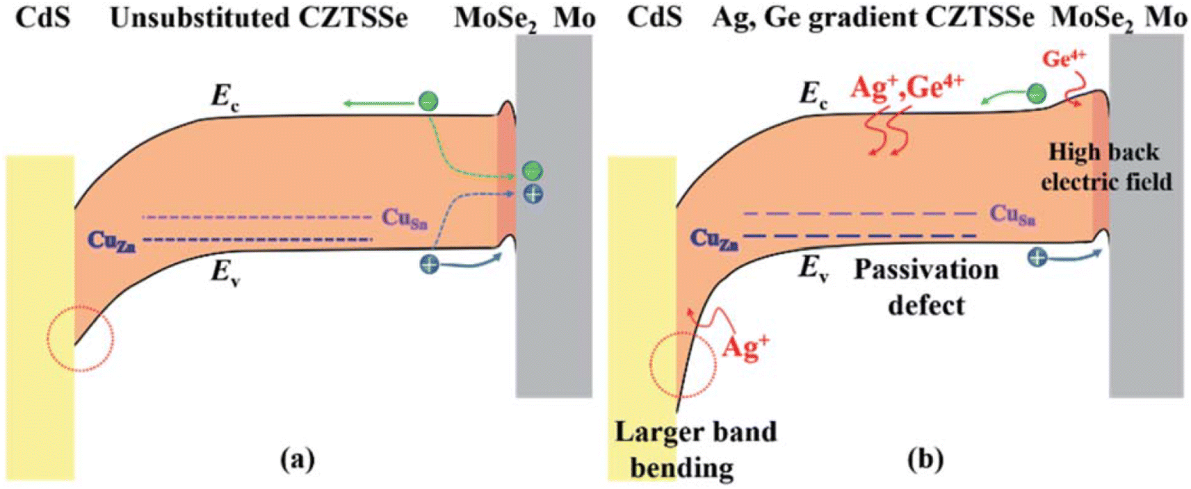 | ||
| Fig. 10 Graphical representation of the band diagram of a CZTSSe solar cell in (a) the standard situation and (b) the Ag,Ge double bandgap gradient situation. Reproduced with permission.111 Copyright 2020, RSC. | ||
As for group 2, a few research teams investigated neighbouring composition ranges,29,41,42,103,104,113,114i.e. mainly towards Ge-rich (x = 0.7) and S–Se mixed (y = 0.5) areas (scattered black stars in Fig. 8). Overall, the obtained performance was lower but promising Shockley–Queisser deficits for Voc and FF were reported for the solution-processed CZTGSSe pioneer studies29,103,104 around the y = 0.5 line in Fig. 8(b) and (d), for a record PCE of 9.4%.104 These devices still underperform as compared to cells from group 1 and the Se-rich part of group 3, due to slightly higher Voc and FF deficits. One possible explanation is their higher S content, as discussed for group 2 devices. Further research is needed to confirm this hypothesis.
This result was obtained mainly through process and composition optimization, more precisely with a control of elemental losses and improved carrier dynamics. It is worth mentioning that other studies managed to process these kesterite compounds either in a low-cost and harmless manner113,114 or on flexible and semi-transparent substrates at low temperature.41,42 Even though reported performance was diminished, this may still pave the way for relevant applications with specific techno-economical requirements. Eventually, given the encouraging SQ deficits and the low number of references in such a large composition region, deeper investigations seem likely to push the performance of corresponding kesterite solar cells to higher levels.
3.4 Pure-Ge
The fourth and last group gathers all the solar cell performances reported for pure-Ge kesterites (x = 1), with particularly poor champion efficiencies below 1% for S-pure CZGS compounds,77,99 likely for the same reasons as group 2. In contrast, Se-pure compounds once again allowed a higher PCE to be reached, overall close to or beyond 6%.49–53,127,128 On the one hand, Ge substitution enables the critical SQ deficit of Voc to be tackled again at the bulk level through a reduction of bulk defect activity and band tailing.50 On the other hand, it is revealed to be ineffective to completely resolve the significant Voc losses appearing at the top and back interfaces, for which surface treatments provide a more adapted solution.49,51,52 The detrimental back contact barrier is also identified through simulations as a main culprit for the poor fill factor globally observed in this case.129 Consequently, combined optimization of buffer material and interface quality is an essential pathway towards higher performance for these wide-bandgap pure-Ge absorbers. This enabled the 8.5% current champion efficiency for CZGSe,49 as well as the efficiency of S–Se mixed CZGSSe with y = 0.3 to increase from 2% to 6% (ref. 92, 93 and 130) (Fig. 11). Besides that, fine tuning of the global stoichiometry remains a key factor with regards to defects and secondary phase formation,53,127 which was investigated in one case with an innovative machine learning-based approach, leading to refined composition ranges for high-yield CZGSe.53 Even though their current efficiency remains strongly limited in comparison with group 1 and 3, these wide bandgap CZGSSe compounds could well fit in the increasingly popular tandem solar cells, as long as a sufficient research effort is provided to solve the aforementioned issues.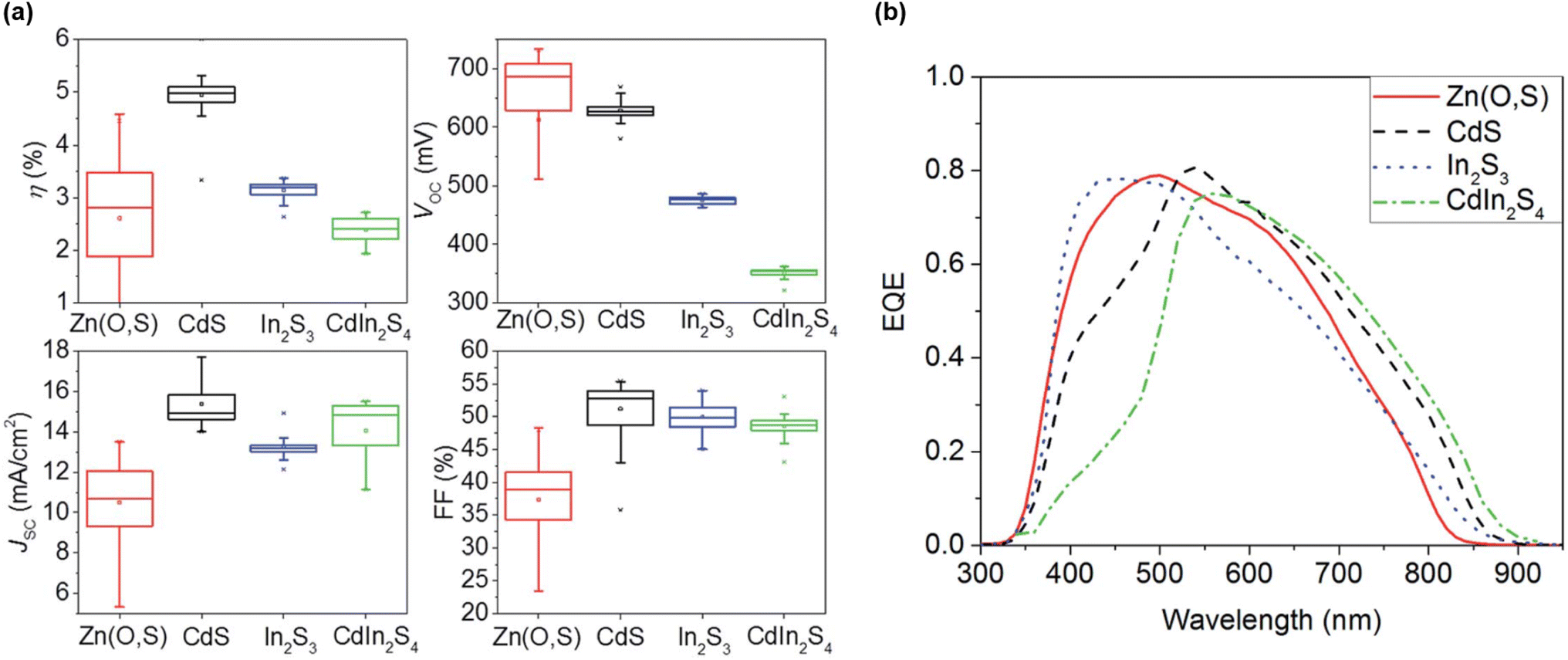 | ||
| Fig. 11 Evolution of CZGSSe solar cell performance for different buffer materials in terms of (a) I–V parameters and (b) EQE response. Adapted from ref. 130 with permission from the Royal Society of Chemistry. | ||
4 Conclusion
The first conclusion that can be drawn from this analysis is that alloying Ge into kesterite absorbers appears to be a promising strategy towards higher solar cell efficiencies, with an actual record slightly beyond 13% for solution-processed CZTGSSe30 while similar performance was recently attained for Ag-incorporated kesterites.10,15,32 This emphasizes the great potential of extrinsic alloying for standard CZTSSe kesterites, even enabling combined approaches such as the successful double Ag,Ge gradient design discussed herein.111 Given similarly well-controlled stoichiometry, Ge alloying provides advantages at both the thin film and solar cell level compared to Ge-free kesterites. First, it modifies the kesterite formation mechanism to favour crystallization dynamics towards greatly improved structural morphology, which increases the fill factor among other things. Second, it strongly mitigates electronic defects as well as crystalline disorder to systematically decrease the Voc deficit of CZTSSe materials, which remains the most critical barrier towards higher performance. Third, it allows Sn–Ge bandgap grading to strengthen carrier collection and increase Jsc, which is arguably less dependent on composition than Voc and FF as visible in Fig. 8. This further highlights the crucial roles of Voc and FF as performance limiting factors in kesterite PV devices, for which this work proposes Ge incorporation as an extremely promising solution.According to this study, the optimal Ge/(Ge + Sn) content should not exceed more than 40%, beyond which most of the positive impacts discussed hereabove tend to be neutralized. Actually, even minute amounts of Ge below 1% tend to bring significant upgrades to kesterite performance. This is particularly well aligned with the critical raw material requirements related to Ge,11 and maintains that kesterites are a more sustainable substitute to replace CIGSe. Besides that, Se-rich composition largely gathers the highest PCEs for CZTGSSe, as already observed widely for kesterite single junctions. All of this then puts in evidence the Ge-low and Se-rich efficiency sweet spot for CZTGSSe, obtained for x = Ge/(Ge + Sn) and y = S/(S + Se), respectively, below 40 and 20%.
The relevance of this conclusion should still be questioned in terms of statistical meaning. Indeed, a large majority of research groups concentrated their efforts only on certain parts of the whole x and y composition domain, likely motivated by the previous theoretical and/or experimental studies. Statistically speaking, the most relevant areas of the composition maps are groups 1 and 3 as shown in Fig. 8, which also tend to be the most successful with regards to performance. Whether this is the consequence of more optimal stoichiometry only or of longer optimization effort too, still needs to be clarified in the future.
The exploration of other composition regions has already been initiated to some extent with promising results, especially for the Voc and FF deficits of group 3 depicted in Fig. 8. Pushing this further may not only help to either challenge or confirm previous assumptions about Ge alloying, but also to better understand the physical reasons explaining the benefits of Ge incorporation. Such studies would then inevitably bring a clearer and more global understanding of the main loss mechanisms affecting kesterites and the best ways to counteract them. Combining this in parallel with the transfer of valuable knowledge between composition regions, e.g. buffer and interface optimization from low-efficiency CZGSSe to high-efficiency CZTSe:Ge, may be one pathway to cross the 14% PCE landmark. Last but not least, investigating other stoichiometries and especially S-rich wide-bandgap compounds would contribute to the development of kesterite-based tandem solar cells,77,131,132 for which the current literature is limited and mostly theoretical.133–135
Author contributions
Conceptualization, R. S.; methodology, R. S.; software, R. S.; validation, R. S., Gi. Bi., and G. B.; formal analysis, R. S.; investigation, R. S.; resources, R. S., G. B. and B. V.; data curation, R. S.; writing—original draft preparation, R. S.; writing—review and editing, R. S., Gi. Bi., G. B., J. d. W, D. F. and B. V.; visualization, R. S.; supervision, G. B., D. F. and B. V.; project administration, G. B. and B. V.; funding acquisition, R. S., Gi. Bi., G. B. and B. V.Conflicts of interest
There are no conflicts to declare.Acknowledgements
This paper is part of the dissemination activities of project CUSTOM-ART, which has received funding from the European Union's Horizon 2020 Research and Innovation Framework Programme under grant agreement No. 952982. R. S. and Gi. Bi. thank FWO for the funding through the Fundamental Research PhD Fellowship (1178022N) and the Junior Postdoctoral Fellowship (1219423N), respectively.References
- G. M. Wilson, M. Al-Jassim, W. K. Metzger, S. W. Glunz, P. Verlinden, G. Xiong, L. M. Mansfield, B. J. Stanbery, K. Zhu, Y. Yan, J. J. Berry, A. J. Ptak, F. Dimroth, B. M. Kayes, A. C. Tamboli, R. Peibst, K. Catchpole, M. O. Reese, C. S. Klinga, P. Denholm, M. Morjaria, M. G. Deceglie, J. M. Freeman, M. A. Mikofski, D. C. Jordan, G. TamizhMani and D. B. Sulas-Kern, J. Phys. D: Appl. Phys., 2020, 53, 493001 CrossRef CAS.
- M. He, C. Yan, J. Li, M. P. Suryawanshi, J. Kim, M. A. Green and X. Hao, Adv. Sci., 2021, 8, 2004313 CrossRef CAS PubMed.
- M. Pagliaro, R. Ciriminna and G. Palmisano, ChemSusChem, 2008, 1, 880–891 CrossRef CAS PubMed.
- E. Biyik, M. Araz, A. Hepbasli, M. Shahrestani, R. Yao, L. Shao, E. Essah, A. C. Oliveira, T. del Caño, E. Rico, J. L. Lechón, L. Andrade, A. Mendes and Y. B. Atlı, Eng., Sci. Technol., 2017, 20, 833–858 Search PubMed.
- G. A. Barron-Gafford, M. A. Pavao-Zuckerman, R. L. Minor, L. F. Sutter, I. Barnett-Moreno, D. T. Blackett, M. Thompson, K. Dimond, A. K. Gerlak, G. P. Nabhan and J. E. Macknick, Nat. Sustain., 2019, 2, 848–855 CrossRef.
- U. P. Singh, Recent Advances in Thin Film Photovoltaics, Springer Nature Singapore, Singapore, 2022, pp. 1–4 Search PubMed.
- M. Baid, A. Hashmi, B. Jain, A. K. Singh, M. A. B. H. Susan and M. Aleksandrova, Opt. Quantum Electron., 2021, 53, 656 CrossRef CAS.
- M. Sahu, V. R. Minnam Reddy, C. Park and P. Sharma, Sol. Energy, 2021, 230, 13–58 CrossRef CAS.
- M. Powalla, S. Paetel, E. Ahlswede, R. Wuerz, C. D. Wessendorf and T. Magorian Friedlmeier, Appl. Phys. Rev., 2018, 5, 041602 Search PubMed.
- M. A. Green, E. D. Dunlop, J. Hohl-Ebinger, M. Yoshita, N. Kopidakis and X. Hao, Prog. Photovoltaics, 2022, 30, 3–12 Search PubMed.
- EU, Critical raw materials, https://single-market-economy.ec.europa.eu/sectors/raw-materials/areas-specific-interest/critical-raw-materials_en, accessed: October, 2022 Search PubMed.
- S. Giraldo, Z. Jehl, M. Placidi, V. Izquierdo-Roca, A. Pérez-Rodríguez and E. Saucedo, Adv. Mater., 2019, 31, 1806692 CrossRef PubMed.
- K. Sun, F. Liu and X. Hao, Thin Films Photovoltaics, IntechOpen, 2022 Search PubMed.
- M. A. Green, E. D. Dunlop, J. Hohl-Ebinger, M. Yoshita, N. Kopidakis, K. Bothe, D. Hinken, M. Rauer and X. Hao, Prog. Photovoltaics, 2022, 30, 687–701 Search PubMed.
- J. Zhou, X. Xu, H. Wu, J. Wang, L. Lou, K. Yin, Y. Gong, J. Shi, Y. Luo, D. Li, H. Xin and Q. Meng, Nat. Energy, 2023, 8, 526–535 CrossRef CAS.
- T. Gershon, D. Bishop, P. Antunez, S. Singh, K. W. Brew, Y. S. Lee, O. Gunawan, T. Gokmen, T. Todorov and R. Haight, Curr. Opin. Green Sustainable Chem., 2017, 4, 29–36 CrossRef.
- J. Li, J. Huang, F. Ma, H. Sun, J. Cong, K. Privat, R. F. Webster, S. Cheong, Y. Yao, R. L. Chin, X. Yuan, M. He, K. Sun, H. Li, Y. Mai, Z. Hameiri, N. J. Ekins-Daukes, R. D. Tilley, T. Unold, M. A. Green and X. Hao, Nat. Energy, 2022, 7, 754–764 CrossRef CAS.
- K. Pal, P. Singh, A. Bhaduri and K. B. Thapa, Sol. Energy Mater. Sol. Cells, 2019, 196, 138–156 CrossRef CAS.
- K. J. Tiwari, S. Giraldo, M. Placidi, Z. Jehl Li-Kao and E. Saucedo, Recent Advances in Thin Film Photovoltaics, Springer Nature Singapore, Singapore, 2022, pp. 41–66 Search PubMed.
- K. Biswas, S. Lany and A. Zunger, Appl. Phys. Lett., 2010, 96, 201902 CrossRef.
- S. Schorr, G. Gurieva, M. Guc, M. Dimitrievska, A. Pérez-Rodríguez, V. Izquierdo-Roca, C. S. Schnohr, J. Kim, W. Jo and J. M. Merino, JPhys Energy, 2019, 2, 012002 CrossRef.
- M. Kumar, A. Dubey, N. Adhikari, S. Venkatesan and Q. Qiao, Energy Environ. Sci., 2015, 8, 3134–3159 RSC.
- Y. E. Romanyuk, S. G. Haass, S. Giraldo, M. Placidi, D. Tiwari, D. J. Fermin, X. Hao, H. Xin, T. Schnabel, M. Kauk-Kuusik, P. Pistor, S. Lie and L. H. Wong, JPhys Energy, 2019, 1, 044004 CrossRef CAS.
- H. Nishihara, T. Maeda, A. Shigemi and T. Wada, Jpn. J. Appl. Phys., 2017, 56, 04CS08 CrossRef.
- R. B. Wexler, G. S. Gautam and E. A. Carter, J. Mater. Chem. A, 2021, 9, 9882–9897 RSC.
- T. Ratz, N. D. Nguyen, G. Brammertz, B. Vermang and J.-Y. Raty, J. Mater. Chem. A, 2022, 10, 4355–4365 RSC.
- Q. Shu, J.-H. Yang, S. Chen, B. Huang, H. Xiang, X.-G. Gong and S.-H. Wei, Phys. Rev. B, 2013, 87, 115208 CrossRef.
- T. Ratz, J.-Y. Raty, G. Brammertz, B. Vermang and N. D. Nguyen, JPhys Energy, 2021, 3, 035005 CrossRef CAS.
- G. M. Ford, Q. Guo, R. Agrawal and H. W. Hillhouse, Chem. Mater., 2011, 23, 2626–2629 CrossRef CAS.
- J. Wang, J. Zhou, X. Xu, F. Meng, C. Xiang, L. Lou, K. Yin, B. Duan, H. Wu, J. Shi, Y. Luo, D. Li, H. Xin and Q. Meng, Adv. Mater., 2022, 34, 2202858 CrossRef CAS PubMed.
- D.-H. Son, S.-H. Kim, S.-Y. Kim, Y.-I. Kim, J.-H. Sim, S.-N. Park, D.-H. Jeon, D.-K. Hwang, S.-J. Sung, J.-K. Kang, K.-J. Yang and D.-H. Kim, J. Mater. Chem. A, 2019, 7, 25279–25289 RSC.
- Y. Gong, Q. Zhu, B. Li, S. Wang, B. Duan, L. Lou, C. Xiang, E. Jedlicka, R. Giridharagopal, Y. Zhou, Q. Dai, W. Yan, S. Chen, Q. Meng and H. Xin, Nat. Energy, 2022, 7, 966–977 CrossRef CAS.
- M. A. Green, E. D. Dunlop, J. Hohl-Ebinger, M. Yoshita, N. Kopidakis and X. Hao, Prog. Photovolt., 2021, 29, 657–667 CrossRef.
- W. Wang, M. T. Winkler, O. Gunawan, T. Gokmen, T. K. Todorov, Y. Zhu and D. B. Mitzi, Adv. Energy Mater., 2014, 4, 1301465 CrossRef.
- C. Yan, J. Huang, K. Sun, S. Johnston, Y. Zhang, H. Sun, A. Pu, M. He, F. Liu, K. Eder, L. Yang, J. M. Cairney, N. J. Ekins-Daukes, Z. Hameiri, J. A. Stride, S. Chen, M. A. Green and X. Hao, Nat. Energy, 2018, 3, 764–772 CrossRef CAS.
- P. Uday Bhaskar, G. Suresh Babu, Y. Kishore Kumar and V. Sundara Raja, Thin Solid Films, 2013, 534, 249–254 CrossRef CAS.
- S. Kim, K. M. Kim, H. Tampo, H. Shibata, K. Matsubara and S. Niki, Sol. Energy Mater. Sol. Cells, 2016, 144, 488–492 CrossRef CAS.
- T. Nagai, T. Shimamura, K. Tanigawa, Y. Iwamoto, H. Hamada, N. Ohta, S. Kim, H. Tampo, H. Shibata, K. Matsubara, S. Niki and N. Terada, ACS Appl. Mater. Interfaces, 2019, 11, 4637–4648 CrossRef CAS PubMed.
- T. Nagai, S. Kim, H. Tampo, K. Tanigawa, Y. Iwamoto, H. Hamada, N. Ohta, H. Shibata, S. Niki and N. Terada, Phys. Status Solidi RRL, 2020, 14, 1900708 CrossRef CAS.
- D. Chen and N. Ravindra, J. Alloys Compd., 2013, 579, 468–472 CrossRef CAS.
- A. Ruiz-Perona, Y. Sánchez, M. Guc, L. Calvo-Barrio, T. Jawhari, J. Merino, M. León and R. Caballero, Sol. Energy, 2020, 199, 864–871 CrossRef CAS.
- A. Ruiz-Perona, Y. Sánchez, M. Guc, S. Khelifi, T. Kodalle, M. Placidi, J. M. Merino, M. León and R. Caballero, Sol. Energy, 2020, 206, 555–563 CrossRef CAS.
- A. Ruiz-Perona, G. Gurieva, M. Sun, T. Kodalle, Y. Sánchez, M. Grossberg, J. M. Merino, S. Schorr, M. León and R. Caballero, J. Alloys Compd., 2021, 868, 159253 CrossRef CAS.
- A. Ruiz-Perona, M. Guc, Y. Sánchez, T. Kodalle, J. M. Merino, M. León and R. Caballero, Sol. Energy, 2021, 226, 251–259 CrossRef CAS.
- R. Caballero, J. Cano-Torres, E. Garcia-Llamas, X. Fontané, A. Pérez-Rodríguez, D. Greiner, C. Kaufmann, J. Merino, I. Victorov, G. Baraldi, M. Valakh, I. Bodnar, V. Izquierdo-Roca and M. León, Sol. Energy Mater. Sol. Cells, 2015, 139, 1–9 CrossRef CAS.
- H. Matsushita, T. Ochiai and A. Katsui, J. Cryst. Growth, 2005, 275, e995–e999 CrossRef CAS.
- M. Buffière, H. ElAnzeery, S. Oueslati, K. Ben Messaoud, G. Brammertz, M. Meuris and J. Poortmans, Thin Solid Films, 2015, 582, 171–175 CrossRef.
- G. Brammertz, T. Kohl, J. De Wild, M. Meuris, B. Vermang and J. Poortmans, Thin Solid Films, 2019, 670, 76–79 CrossRef CAS.
- L. Choubrac, M. Bär, X. Kozina, R. Félix, R. G. Wilks, G. Brammertz, S. Levcenko, L. Arzel, N. Barreau, S. Harel, M. Meuris and B. Vermang, ACS Appl. Energy Mater., 2020, 3, 5830–5839 CrossRef CAS.
- S. Sahayaraj, G. Brammertz, B. Vermang, T. Schnabel, E. Ahlswede, Z. Huang, S. Ranjbar, M. Meuris, J. Vleugels and J. Poortmans, Sol. Energy Mater. Sol. Cells, 2017, 171, 136–141 CrossRef CAS.
- N. Benhaddou, S. Aazou, Y. Sánchez, J. Andrade-Arvizu, I. Becerril-Romero, M. Guc, S. Giraldo, V. Izquierdo-Roca, E. Saucedo and Z. Sekkat, Sol. Energy Mater. Sol. Cells, 2020, 216, 110701 CrossRef CAS.
- I. Anefnaf, S. Aazou, Y. Sánchez, P. Vidal-Fuentes, R. Fonoll-Rubio, K. J. Tiwari, S. Giraldo, Z. J. Li-Kao, J. Andrade-Arvizu, M. Guc, E. Saucedo and Z. Sekkat, Sol. Energy Mater. Sol. Cells, 2021, 227, 111106 CrossRef CAS.
- E. Grau-Luque, I. Anefnaf, N. Benhaddou, R. Fonoll-Rubio, I. Becerril-Romero, S. Aazou, E. Saucedo, Z. Sekkat, A. Perez-Rodriguez, V. Izquierdo-Roca and M. Guc, J. Mater. Chem. A, 2021, 9, 10466–10476 RSC.
- G. Swapna Mary, D. R. Nagapure, R. M. Patil, G. Hema Chandra, M. Anantha Sunil, R. Prasada Rao, M. Gupta and Y. Venkata Subbaiah, Vacuum, 2016, 131, 264–270 CrossRef CAS.
- C. Sripan, V. E. Madhavan, R. Ganesan and A. K. Viswanath, Surf. Interfaces, 2017, 7, 134–138 CrossRef CAS.
- L. Huang, H. Deng, J. He, X. Meng, J. Tao, H. Cao, L. Sun, P. Yang and J. Chu, Mater. Lett., 2015, 159, 1–4 CrossRef CAS.
- M. Courel, T. G. Sanchez, N. R. Mathews and X. Mathew, J. Phys. D: Appl. Phys., 2018, 51, 095107 CrossRef.
- N. Saini, N. M. Martin, J. K. Larsen, A. Hultqvist, T. Törndahl and C. Platzer-Björkman, Sol. RRL, 2022, 6, 2100837 CrossRef CAS.
- T. Kohl, G. Brammertz, J. de Wild, M. Neuwirth, M. Meuris, J. Poortmans and B. Vermang, Thin Solid Films, 2018, 660, 247–252 CrossRef CAS.
- S. Giraldo, M. Neuschitzer, T. Thersleff, S. López-Marino, Y. Sánchez, H. Xie, M. Colina, M. Placidi, P. Pistor, V. Izquierdo-Roca, K. Leifer, A. Pérez-Rodríguez and E. Saucedo, Adv. Energy Mater., 2015, 5, 1501070 CrossRef.
- S. Giraldo, M. Neuschitzer, M. Placidi, P. Pistor, A. Perez-Rodriguez and E. Saucedo, IEEE J. Photovolt., 2016, 6, 754–759 Search PubMed.
- S. Giraldo, T. Thersleff, G. Larramona, M. Neuschitzer, P. Pistor, K. Leifer, A. Pérez-Rodríguez, C. Moisan, G. Dennler and E. Saucedo, Prog. Photovolt., 2016, 24, 1359–1367 CrossRef CAS.
- S. Giraldo, E. Saucedo, M. Neuschitzer, F. Oliva, M. Placidi, X. Alcobé, V. Izquierdo-Roca, S. Kim, H. Tampo, H. Shibata, A. Pérez-Rodríguez and P. Pistor, Energy Environ. Sci., 2018, 11, 582–593 RSC.
- S. Giraldo, S. Kim, J. A. Andrade-Arvizu, X. Alcobé, C. Malerba, M. Valentini, H. Tampo, H. Shibata, V. Izquierdo-Roca, A. Pérez-Rodríguez and E. Saucedo, Prog. Photovolt., 2019, 27, 779–788 CrossRef CAS.
- M. Neuschitzer, J. Marquez, S. Giraldo, M. Dimitrievska, M. Placidi, I. Forbes, V. Izquierdo-Roca, A. Pérez-Rodriguez and E. Saucedo, J. Phys. Chem. C, 2016, 120, 9661–9670 CrossRef CAS.
- M. Neuschitzer, M. E. Rodriguez, M. Guc, J. A. Marquez, S. Giraldo, I. Forbes, A. Perez-Rodriguez and E. Saucedo, J. Mater. Chem. A, 2018, 6, 11759–11772 RSC.
- M. Ritzer, S. Schönherr, P. Schöppe, W. Wisniewski, S. Giraldo, G. Gurieva, A. Johannes, C. T. Plass, K. Ritter, G. Martínez-Criado, S. Schorr, E. Saucedo, C. Ronning and C. S. Schnohr, ACS Appl. Energy Mater., 2020, 3, 558–564 CrossRef CAS.
- J. Márquez, H. Stange, C. J. Hages, N. Schaefer, S. Levcenko, S. Giraldo, E. Saucedo, K. Schwarzburg, D. Abou-Ras, A. Redinger, M. Klaus, C. Genzel, T. Unold and R. Mainz, Chem. Mater., 2017, 29, 9399–9406 CrossRef.
- J. González-Castillo, F. Pulgarín-Agudelo, E. Rodríguez-González, O. Vigil-Galán, M. Courel-Piedrahita and J. Andrade-Arvizu, Mater. Sci. Semicond. Process., 2018, 83, 96–101 CrossRef.
- J. Andrade-Arvizu, R. Fonoll-Rubio, Y. Sánchez, I. Becerril-Romero, C. Malerba, M. Valentini, L. Calvo-Barrio, V. Izquierdo-Roca, M. Placidi, O. Vigil-Galán, A. Pérez-Rodríguez, E. Saucedo and Z. Jehl Li-Kao, ACS Appl. Energy Mater., 2020, 3, 10362–10375 CrossRef CAS.
- C. Andres, A. Cabas-Vidani, A. Tiwari and Y. Romanyuk, Thin Solid Films, 2018, 665, 168–172 CrossRef CAS.
- J. Liu, Z. Liu, K. Gao, H. Cai, Y. Liu, W. Zhao, X. Liu, K. Cheng and Z. Du, ACS Appl. Mater. Interfaces, 2021, 13, 56302–56308 CrossRef CAS PubMed.
- D. Nowak, T. Khonsor, D. Pareek and L. Gütay, Appl. Sci., 2022, 12, 1376 CrossRef CAS.
- S. Padhy, V. Kumar, N. B. Chaure and U. P. Singh, Mater. Sci. Semicond. Process., 2022, 138, 106276 CrossRef CAS.
- J. Chen, W. Li, C. Yan, S. Huang and X. Hao, J. Alloys Compd., 2015, 621, 154–161 CrossRef CAS.
- N. Saini, J. K. Larsen, K. V. Sopiha, J. Keller, N. Ross and C. Platzer-Björkman, Phys. Status Solidi A, 2019, 216, 1900492 CrossRef CAS.
- N. Saini, J. K. Larsen, K. Lindgren, A. Fazi and C. Platzer-Björkman, J. Alloys Compd., 2021, 880, 160478 CrossRef CAS.
- K.-S. Lim, S.-M. Yu, S. Seo, H. Shin, T.-S. Oh and J.-B. Yoo, Mater. Sci. Semicond. Process., 2019, 89, 194–200 CrossRef CAS.
- T. Sanchez, E. Regalado-Pérez, X. Mathew, M. Sanchez, Y. Sanchez, E. Saucedo and N. Mathews, Sol. Energy Mater. Sol. Cells, 2019, 198, 44–52 CrossRef CAS.
- J. Li, H. Shen, H. Shang, Y. Li and W. Wu, Mater. Lett., 2017, 190, 188–190 CrossRef CAS.
- L. Sun, H. Shen, H. Huang, A. Raza, Q. Zhao and J. Yang, Vacuum, 2019, 165, 186–192 CrossRef CAS.
- Y. Gong, Y. Zhang, Q. Zhu, Y. Zhou, R. Qiu, C. Niu, W. Yan, W. Huang and H. Xin, Energy Environ. Sci., 2021, 14, 2369–2380 RSC.
- D. B. Khadka, S. Kim and J. Kim, J. Phys. Chem. C, 2016, 120, 4251–4258 CrossRef CAS.
- B. H. Lee, K. S. Gour, V. Karade, J. S. Jang, J. Kim, E. Jo, M. G. Gang, D. M. Lee, I. J. Lee, J. Park and J. H. Kim, Mater. Lett., 2021, 284, 128981 CrossRef CAS.
- L. Du, W. Zhao, Y. Sun, L. Liu, W. Dai, Z. Liu, G. Fu, W. Yu and C. Gao, J. Alloys Compd., 2018, 737, 184–188 CrossRef CAS.
- A. Lokhande, R. Chalapathy, J. Jang, P. Babar, M. Gang, C. Lokhande and J. H. Kim, Sol. Energy Mater. Sol. Cells, 2017, 161, 355–367 CrossRef CAS.
- M. Grossberg, K. Timmo, T. Raadik, E. Kärber, V. Mikli and J. Krustok, Thin Solid Films, 2015, 582, 176–179 CrossRef CAS.
- G. Gurieva, D. Többens, M. Y. Valakh and S. Schorr, J. Phys. Chem. Solids, 2016, 99, 100–104 CrossRef CAS.
- S. Niedenzu, G. Gurieva and S. Schorr, Thin Solid Films, 2019, 669, 625–628 CrossRef CAS.
- D. B. Khadka and J. Kim, CrystEngComm, 2013, 15, 10500 RSC.
- A. M. Ayala, N. Mathews, M. Pal, G. K. Gupta, A. Dixit and X. Mathew, Thin Solid Films, 2019, 676, 68–74 CrossRef CAS.
- T. Schnabel, M. Seboui and E. Ahlswede, RSC Adv., 2017, 7, 26–30 RSC.
- T. Schnabel, M. Seboui and E. Ahlswede, Energies, 2017, 10, 1813 CrossRef.
- S. Bag, O. Gunawan, T. Gokmen, Y. Zhu and D. B. Mitzi, Chem. Mater., 2012, 24, 4588–4593 CrossRef CAS.
- Z. Zhang, Q. Gao, J. Guo, Y. Zhang, Y. Han, J. Ao, M.-J. Jeng, F. Liu, W. Liu and Y. Zhang, Sol. RRL, 2020, 4, 2000059 CrossRef CAS.
- Y. Han, J. Ao, Z. Zhang, Q. Gao, J. Guo, W. Liu, F. Liu and Y. Zhang, ACS Appl. Energy Mater., 2021, 4, 11793–11801 CrossRef CAS.
- D. B. Khadka and J. Kim, J. Phys. Chem. C, 2015, 119, 1706–1713 CrossRef CAS.
- M. Singh, T. R. Rana and J. Kim, J. Alloys Compd., 2016, 675, 370–376 CrossRef CAS.
- G. Chen, W. Wang, S. Chen, Z. Whang, Z. Huang, B. Zhang and X. Kong, J. Alloys Compd., 2017, 718, 236–245 CrossRef CAS.
- I. Kim, K. Kim, Y. Oh, K. Woo, G. Cao, S. Jeong and J. Moon, Chem. Mater., 2014, 26, 3957–3965 CrossRef CAS.
- S. Sun, J. Guo, R. Hao, B. Liu, H. Liu, G. Wei, X. Ma, X. Li, S. Fang and Y. Wang, International Conference on Optoelectronic and Microelectronic Technology and Application, Nanjing, China, 2020, p. 165 Search PubMed.
- C. Aytug Ava, Y. S. Ocak, S. Asubay and O. Celik, Opt. Mater., 2021, 121, 111565 CrossRef CAS.
- Q. Guo, G. M. Ford, W.-C. Yang, C. J. Hages, H. W. Hillhouse and R. Agrawal, Sol. Energy Mater. Sol. Cells, 2012, 105, 132–136 CrossRef CAS.
- C. J. Hages, S. Levcenco, C. K. Miskin, J. H. Alsmeier, D. Abou-Ras, R. G. Wilks, M. Bär, T. Unold and R. Agrawal, Prog. Photovolt., 2015, 23, 376–384 CrossRef CAS.
- A. S. R. Chesman, J. van Embden, E. Della Gaspera, N. W. Duffy, N. A. S. Webster and J. J. Jasieniak, Chem. Mater., 2014, 26, 5482–5491 CrossRef CAS.
- A. D. Collord and H. W. Hillhouse, Chem. Mater., 2016, 28, 2067–2073 CrossRef CAS.
- Q. Yi, J. Wu, J. Zhao, H. Wang, J. Hu, X. Dai and G. Zou, ACS Appl. Mater. Interfaces, 2017, 9, 1602–1608 CrossRef CAS PubMed.
- W. Zhao, D. Pan and S. F. Liu, Nanoscale, 2016, 8, 10160–10165 RSC.
- Y. Sun, L. Du, Z. Liu, W. Ding, C. Gao and W. Yu, Mater. Lett., 2017, 195, 76–78 CrossRef CAS.
- C. Gao, Y. Sun and W. Yu, Coatings, 2018, 8, 304 CrossRef.
- J. Fu, D. Kou, W. Zhou, Z. Zhou, S. Yuan, Y. Qi and S. Wu, J. Mater. Chem. A, 2020, 8, 22292–22301 RSC.
- Y. Deng, Z. Zhou, X. Zhang, L. Cao, W. Zhou, D. Kou, Y. Qi, S. Yuan, Z. Zheng and S. Wu, J. Energy Chem., 2021, 61, 1–7 CrossRef CAS.
- X. Lv, C. Zhu, H. Hao, R. Liu, Y. Wang and J. Wang, Ceram. Int., 2020, 46, 25638–25645 CrossRef CAS.
- P. Punathil, E. Artegiani, S. Zanetti, L. Lozzi, V. Kumar and A. Romeo, Sol. Energy, 2022, 236, 599–607 CrossRef CAS.
- X. Peng, S. Zhang and Y. Xiang, J. Alloys Compd., 2015, 640, 75–81 CrossRef CAS.
- F. Li, Z. Xia and Q. Liu, J. Phys. Chem. C, 2016, 120, 16969–16976 CrossRef CAS.
- F. E. Cancino-Gordillo, J. V. Cab and U. Pal, Appl. Surf. Sci., 2022, 571, 151261 CrossRef CAS.
- D. Mora-Herrera, M. Pal and F. Paraguay-Delgado, Mater. Chem. Phys., 2021, 257, 123764 CrossRef CAS.
- Y. Li, W. Ling, Q. Han and W. Shi, RSC Adv., 2014, 4, 55016–55022 RSC.
- J. Li, X. Gao, L. Han, X. Yang and H. Liu, Mater. Lett., 2016, 163, 111–114 CrossRef CAS.
- W. Shockley and H. J. Queisser, J. Appl. Phys., 1961, 32, 510–519 CrossRef CAS.
- S. Rühle, Sol. Energy, 2016, 130, 139–147 CrossRef.
- S. Lee, K. J. Price, E. Saucedo and S. Giraldo, Sol. Energy, 2019, 194, 114–120 CrossRef CAS.
- S. Lee, K. J. Price and E. Saucedo, J. Phys. D: Appl. Phys., 2021, 54, 335501 CrossRef CAS.
- H.-S. Duan, W. Yang, B. Bob, C.-J. Hsu, B. Lei and Y. Yang, Adv. Funct. Mater., 2013, 23, 1466–1471 CrossRef CAS.
- S. Kim, K. M. Kim, H. Tampo, H. Shibata and S. Niki, Appl. Phys. Express, 2016, 9, 102301 CrossRef.
- R. Gunder, J. A. Márquez-Prieto, G. Gurieva, T. Unold and S. Schorr, CrystEngComm, 2018, 20, 1491–1498 RSC.
- L. Choubrac, G. Brammertz, N. Barreau, L. Arzel, S. Harel, M. Meuris and B. Vermang, Phys. Status Solidi A, 2018, 215, 1800043 CrossRef.
- S. Yang, S. Khelifi, G. Brammertz, L. Choubrac, N. Barreau, P. Bolt, B. Vermang and J. Lauwaert, J. Phys. D: Appl. Phys., 2020, 53, 385102 CrossRef CAS.
- T. Schnabel, M. Seboui, A. Bauer, L. Choubrac, L. Arzel, S. Harel, N. Barreau and E. Ahlswede, RSC Adv., 2017, 7, 40105–40110 RSC.
- B. Vermang, G. Brammertz, M. Meuris, T. Schnabel, E. Ahlswede, L. Choubrac, S. Harel, C. Cardinaud, L. Arzel, N. Barreau, J. van Deelen, P.-J. Bolt, P. Bras, Y. Ren, E. Jaremalm, S. Khelifi, S. Yang, J. Lauwaert, M. Batuk, J. Hadermann, X. Kozina, E. Handick, C. Hartmann, D. Gerlach, A. Matsuda, S. Ueda, T. Chikyow, R. Félix, Y. Zhang, R. G. Wilks and M. Bär, Sustainable Energy Fuels, 2019, 3, 2246–2259 RSC.
- S. Khelifi, G. Brammertz, L. Choubrac, M. Batuk, S. Yang, M. Meuris, N. Barreau, J. Hadermann, H. Vrielinck, D. Poelman, K. Neyts, B. Vermang and J. Lauwaert, Sol. Energy Mater. Sol. Cells, 2021, 219, 110824 CrossRef CAS.
- A. D. Adewoyin, M. A. Olopade, O. O. Oyebola and M. A. Chendo, Optik, 2019, 176, 132–142 CrossRef CAS.
- M. Umehara, S. Tajima, Y. Takeda and T. Motohiro, J. Alloys Compd., 2016, 689, 713–717 CrossRef CAS.
- M. Jamil, A. Ali, K. Mahmood, M. I. Arshad, S. Tahir, M. Ajaz un Nabi, S. Ikram, N. Amin and S. Hussain, J. Alloys Compd., 2020, 821, 153221 CrossRef CAS.
Footnote |
| † Electronic supplementary information (ESI) available. See DOI: https://doi.org/10.1039/d3ta01218b |
| This journal is © The Royal Society of Chemistry 2023 |