
 Open Access Article
 This Open Access Article is licensed under a Creative Commons Attribution-Non Commercial 3.0 Unported Licence
In situ TEM analysis of reversible non-180° domain switching in (K,Na)NbO3 single crystals†
Qinwen
Guo
ab,
Chengpeng
Hu
 d,
Xiangfei
Li
ab,
Ying
Meng
ac,
Luyao
Wang
ab,
Haoyu
Zhuang
ac,
Xi
Shen
*a,
Yuan
Yao
a,
Hao
Tian
d,
Zhongxiang
Zhou
*d and
Richeng
Yu
*ace
d,
Xiangfei
Li
ab,
Ying
Meng
ac,
Luyao
Wang
ab,
Haoyu
Zhuang
ac,
Xi
Shen
*a,
Yuan
Yao
a,
Hao
Tian
d,
Zhongxiang
Zhou
*d and
Richeng
Yu
*ace
aBeijing National Laboratory for Condensed Matter Physics, Institute of Physics, Chinese Academy of Sciences, Beijing 100190, P. R. China. E-mail: xshen@iphy.ac.cn; rcyu@iphy.ac.cn
bCollege of Material Science and Opto-Electronic Technology, University of Chinese Academy of Sciences, Beijing 100190, P. R. China
cSchool of Physical Sciences, University of Chinese Academy of Sciences, Beijing 100049
dSchool of Physics, Harbin Institute of Technology, Harbin 150001, P. R. China. E-mail: zhouzx@hit.edu.cn
eSongshan Lake Materials Laboratory, Dongguan, Guangdong 523808, P. R. China
First published on 18th April 2023
Abstract
Reversible non-180° domain switching is believed to be able to enhance the electromechanical performances of piezoelectrics. However, the slow improvement of strain performances of (K,Na)NbO3 (KNN) is caused by an inadequate understanding of reversible non-180° domain switching. Here, with an electric field-available sample holder, we directly observe the reversible domain wall motion by in situ transmission electron microscopy and non-180° domain switching in a compositionally graded KNN single crystal which has an ultrahigh large-signal piezoelectric coefficient. The characteristics of domain wall motion under varying electric fields are investigated. The analysis of high-angle annular dark-field images with an atomic resolution indicates that local compositional fluctuation, strain fluctuation and polarization rotation exist in the domains. We propose that the restoring force derives from the built-in flexoelectric effect caused by compositional fluctuation at the atomic scale. The new mechanism paves the way for enhancing the piezoelectric properties and designing high performance piezoelectrics.
Introduction
Piezoelectric materials have the function of converting mechanical energy into electrical energy or vice versa, so they are widely used in ultrasonic transducers and actuators,1,2 especially in the fields of medical care,3 industry and advanced scientific research equipment, such as transmission electron microscopes and scanning tunneling microscopes. One of the most excellent piezoelectric materials is ferroelectrics, represented by a series of lead-based piezoelectric ceramics such as Pb(Zr,Ti)O3. Owing to their outstanding piezoelectric performance and electromechanical coupling factor,1 lead-based piezoelectric ceramics have dominated the market for several decades. However, when blood lead is over 1.93 μmol L−1, lead toxicity can lead to a series of serious human diseases.4 Due to increasing concern for human health and environmental protection, the application of lead-based materials is restricted by many regulations, such as the Restriction of the use of certain Hazardous Substances (RoHS). Therefore, in recent years, the demand for high-performance lead-free piezoelectric materials has increased rapidly.One of the most promising substitutes for lead-based piezoelectric ceramics is potassium sodium niobite [(K,Na)NbO3 (KNN)] because it has a moderate piezoelectric coefficient d33 = 80 pC N−1 and high Curie temperature TC = 420 °C.5 Pioneering research was carried out in 2004. Saito et al. achieved a high piezoelectric coefficient d33 = 416 pC N−1 in a composition of Li,Ta,Sb-modified potassium sodium niobate textured ceramic, which is comparable to that in commercial soft PZT4 ceramic.6 The high piezoelectric coefficient partly stems from an orthorhombic–tetragonal (O–T) phase boundary. Later, some researchers improved d33 of KNN-based ceramics to more than 490 pC N−1 by phase boundary engineering (PBE).7–13 However, the dopant-induced polymorphic phase transition (PPT) moves down to room temperature, which reduces the Curie temperature. Subsequently, the improvement of piezoelectric coefficient d33 by PBE is at the expense of temperature stability.
The strain performance of a KNN-based piezoelectric material improves much more slowly than its piezoelectric coefficient d33.14 Piezoelectric materials possessing two extraordinary phenomena could show sizeable electric field-induced strain. The first one is electric field-induced phase transition. For example, Liu et al. reported an ultra-high large-signal piezoelectric coefficient  of 1400 pm V−1 in BNT-2.5Nb and observed an electric field-induced phase transition by in situ TEM.15 Recently, electric field-induced phase transition between the orthorhombic phase and tetragonal phase in KNN-based piezoceramics was reported by Zhang et al.16 The other one is reversible non-180° domain switching. Generally, domain switching is an irrecoverable or one-time effect because it lacks the necessary restoring force to overcome or change the energy barrier between equivalent polarization orientations. Fortunately, some researchers realized reversible domain switching by introducing restoring force. In 2004, Ren et al. reported that point-defects generated by acceptor impurity occupying B sites in BaTiO3 can provide an intrinsic restoring force to make domain switching reversible.17,18 In 2015, Khansur et al. found largely reversible electric field-induced non-180° ferroelectric domain switching in microstructurally engineered material BaTiO3–KNbO3 by in situ high energy X-ray diffraction,19 and they suggested that the residual stress built up in non-polar oriented grains can completely reverse the domain wall motion without the aid of any external bias. In 2021, Zhang et al. used a two-step sintering process to introduce ferroelectric–paraelectric heterogeneous structures into a doped KNN. The result of phase-field simulations shows that the depolarization energy enhanced by polar–nonpolar interfaces can act as a restoring force to drive the domain to the initial state.20 Recently, Hu et al. grew a compositionally graded KNN single crystal (∼K0.43Na0.57NbO3) by using the top-seeded solution-growth method.21 The material has an ultrahigh large-signal piezoelectric coefficient
  of 9000 pm V−1, which is much larger than the highest value ever reported in lead-based single crystals (∼2500 pm V−1).22 Though high strain properties are attributed to reversible non-180° domain switching, the process of reversible domain switching has not been directly verified yet. For the compositionally graded KNN, the restoring force is considered to be the compositional gradient-induced stress, which is in fact related to the flexoelectric effect.23,24 Generally, owing to the size effect, the flexoelectric effect is so weak that it can be ignored in bulk materials. Subsequently, the flexoelectric effects have been investigated mainly in nanoscale systems, such as thin film.25 Therefore, attention should be paid to the built-in flexoelectric effect in bulk materials.
In this work, we carry out in situ transmission electron microscopy (TEM) studies of the compositionally graded KNN single crystals by using an electric field available sample holder. The reversible domain wall motion and non-180° domain switching can be clearly shown by bright-field (BF) images. The behavior of domain wall motion under a varying electric field is investigated in this work. The built-in flexoelectric effect generating restoring force is studied at the atomic scale by using high-angle annular dark-field scanning transmission electron microscopy (HAADF-STEM).
Experimental details
TEM specimen fabrication
Specimens for TEM observations were prepared using an FEI Helios 600I focused ion beam (FIB). The specimens were soldered by Pt deposition on the electric chip. Prior to milling the sample, a Pt protective layer was deposited, and after thickness was reduced, a shallow beam voltage/current of 2 kV/10 pA was used to remove damaged layer and implanted Ga+ ions. The KNN single crystals were grown by using the top-seeded solution-growth method, of which more details can be found in the literature.21TEM characterization and analysis
In situ electric field-available TEM and STEM experiments were conducted with a JEOL ARM200F TEM (200 keV) equipped with double Cs correctors (CEOS) for the condenser lens and objective lens. The high-angle annular dark-field (HAADF) images were acquired at acceptance semi-angles of 90–370 mrad. The strain mapping analyses were carried out by using the software Peak Pairs Analysis. Prior to the analysis, the indispensable filter used in the analysis proccess is a real space noise filter—low pass filter.26 Atomic positions and intensities were determined by the multiple-ellipse fitting (MEF) method through using the CalAtom Software developed by Prof. Fang Lin. The Gaussian filter was used prior to the analysis of atomic positions and intensities.Results and discussion
Specimens for TEM observations were prepared using a focused ion beam (FIB) and placed on an electric chip with four electrodes as shown in Fig. 1. Fig. 2 shows a bright-field image of the domain morphology of the KNN single crystal at the initial stage. Five lamellar-shaped domains indexed to series A1–A5 are embedded in the matrix domain. The inset shows a selected area electron diffraction (SAED) pattern and the split that can be seen clearly in high-order diffraction spots, indicating the difference in crystallographic orientation between the two neighboring domains. The lamellar domains have a width range of 0.13–0.59 μm, and the contrast of domain walls consists of fringes indicating that the domain walls are inclined to the surface of the specimen. The domain walls are not strictly parallel to each other, so that the lamellar domains are wedge-shaped. This may be caused by the presence of charges or shear stress.27 Restricted by the mechanical compatibility conditions,28 the crystallographic orientations of the ferroelectric domain wall are not arbitrary and they are summarized in the literature.29 Therefore, the traces of domain walls indicate the angle of the polarization vectors of the neighboring domains. In Fig. 2, the traces of the domain walls are identified as being oriented in the [3![[1 with combining macron]](https://www.rsc.org/images/entities/char_0031_0304.gif) 0]C direction, which means that the domain walls are 120° or 60° domain walls (S2-wall) and indexed to 〈13
0]C direction, which means that the domain walls are 120° or 60° domain walls (S2-wall) and indexed to 〈13![[3 with combining macron]](https://www.rsc.org/images/entities/char_0033_0304.gif) 〉C, which is consistent with the result reported previously.30 Considering that the S2-wall of the 120° domain wall is charged, we prefer to regard it as 60° domain configuration. Possible polarization orientations are marked with arrows in Fig. 2.
〉C, which is consistent with the result reported previously.30 Considering that the S2-wall of the 120° domain wall is charged, we prefer to regard it as 60° domain configuration. Possible polarization orientations are marked with arrows in Fig. 2.
 | ||
| Fig. 1 Schematic diagram of an electric chip in TEM. | ||
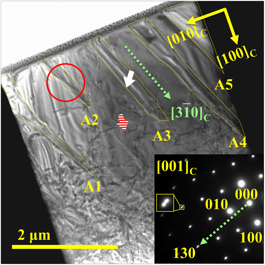 | ||
| Fig. 2 Bright-field (BF) image and selected area electron diffraction (SAED) pattern of 60° domains along the [001]C zone axis. The five domains marked by yellow dashed lines have approximately parallel traces of domain walls. They have an identical orientation of polarization and are marked as A1–A5, respectively. The SAED pattern is acquired from the area circled in red and shows the splitting of diffraction points. The green dashed line roughly pointing to (130)* in the SAED pattern is a vertical line to the traces of the five domain walls. Therefore, the orientation index of the trace is approximately [30]C as shown by another green dashed line in the BF. Two short arrows indicate possible polarization vector directions on the two sides of the domain wall, judged by the orientation of domain walls. The white arrow indicates the [110]C direction of A domains. The arrow with red lines indicates that the polarization vector of the matrix domain is along the [101]C direction, which is out of the plane. | ||
A series of bright-field TEM micrographs (Fig. 3) show reversible domain wall motions under electric fields. An electric field perpendicular to the electron beam is applied to the TEM sample surface as indicated by the yellow arrow in Fig. 3b. At 10 V, the domain morphology has little change. With the increase of applied electric field, the vertices of the five A domains remain steady, but lateral movements of the walls occur in all the A domains. At 19 V, all the A domains undergo domain wall lateral movements and are more expansive than at the initial stage, indicating domain switching from the matrix domain to A domains. Furthermore, a wedge-shaped domain nucleates beside A1 (Fig. 3c). When a maximum voltage of 24 V is applied in this study, the widths of all the A domains reach their maximum values (Fig. 3d). Accompanied by the lateral movement of the domain wall, domains A4 and A5 are merged together. Moreover, the wedge-shaped domain that nucleated near A1 obviously expands. This evolution implies that the applied electric field is beneficial to the polarization of A domains and proves the rationality of polarization orientation suggested above.
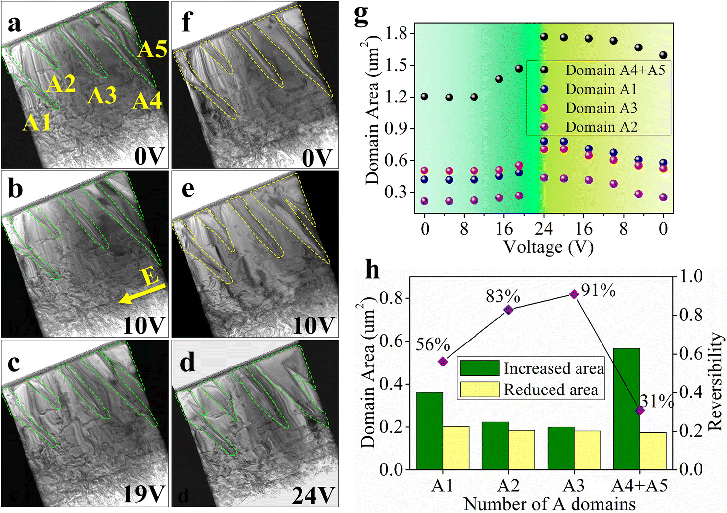 | ||
| Fig. 3 TEM images of the reversible 60° domain along the [001]C zone axis. (a–f) Reversible domain wall motions of A domains under different electric field strengths. (g) Domain area for each of A domains under different electric field strengths. (h) Total varied domain area for each of A domains in the range of 0–24 V and 24–0 V, respectively. Reversibility is defined as the ratio of “reduced area” and “increased area”. | ||
Generally, domain switching is irreversible because different domains have identical energy. However, reversible domain wall motion is observed when the electric field decreases gradually. At a voltage of 10 V, there are some noticeable changes as presented in Fig. 3e. Merging of A4 and A5 begins to disappear, which is indicated by the contrast of recovered domain walls, during which the matrix domain grows. Fig. 3f shows the domain pattern at 0 V. The domains A4 and A5 are completely separated, and the nucleation beside A1 disappears. The area of all the A domains decreases as the applied electric field decreases, accompanied by the motion of domain walls, which is contrary to the scenario in the case of increasing electric field.
To further explore the motion characteristics of domains with varying electric fields, the domain areas of all the A domains under different external fields are measured as shown in Fig. 3g. It can be seen that the evolution behaviors of all the A domains are the same while the domain areas increase nonuniformly with voltage increasing from 0 to 24 V. The area remains almost unchanged in the range of 0–10 V, indicating the coercive voltage is larger than 10 V. In the range of 10–19 V, the area increases moderately, and in the range of 19–24 V, the area increases more sharply and significantly. On the other hand, with the decrease of electric field, the reverse movement of domain wall is smoother. In the range of 24–20 V, the area remains almost unchanged and decreases uniformly in the range of 20–0 V. As indicated in Fig. 3h, none of the A domains is recovered to the initial state completely. The reversibility of the domain varies from 31% for (A4 + A5) to 91% for A3.
STEM EDX mapping is carried out at the nanoscale and the results are shown in Fig. S1.† The results confirm that the distributions of various elements are uniform and no obvious composition gradients for K or Na atoms are observed at the nanoscale. Fig. S2† shows an HAADF-STEM image at the atomic scale. Owing to the heavier atomic mass of Nb atoms, the brighter spots represent Nb atomic columns and the darker spots represent K/Na atomic columns. Fig. 4a shows a unit-cell of KNN: the K/Na atom occupies the A site, while the Nb atom takes the B site. The results of atomic column intensity statistics (Fig. S3a†) show that there are distinct intensity distributions for the atomic columns of the A site and B site. It can be seen that the intensity distribution of the A site is more dispersive than that of the B site, which is caused by compositional fluctuation. The different intensities of atomic columns at the A site reflect the relative content of K and Na elements because the intensity in the HAADF image is proportional to Z1.7, where Z is the atomic number. A site intensity map is shown in Fig. 4b based on the analysis of atomic positions and intensities (Fig. S3b†). It can be seen that the abundant K or Na atomic columns are randomly distributed, indicating the existence of compositional fluctuation at the atomic scale. Though the composition has a macroscopic gradient in the single crystal characterized by electron microprobe analysis,21 our results show that the compositional gradient is inconspicuous but the composition fluctuation is significant at the atomic scale as shown in Fig. 4b.
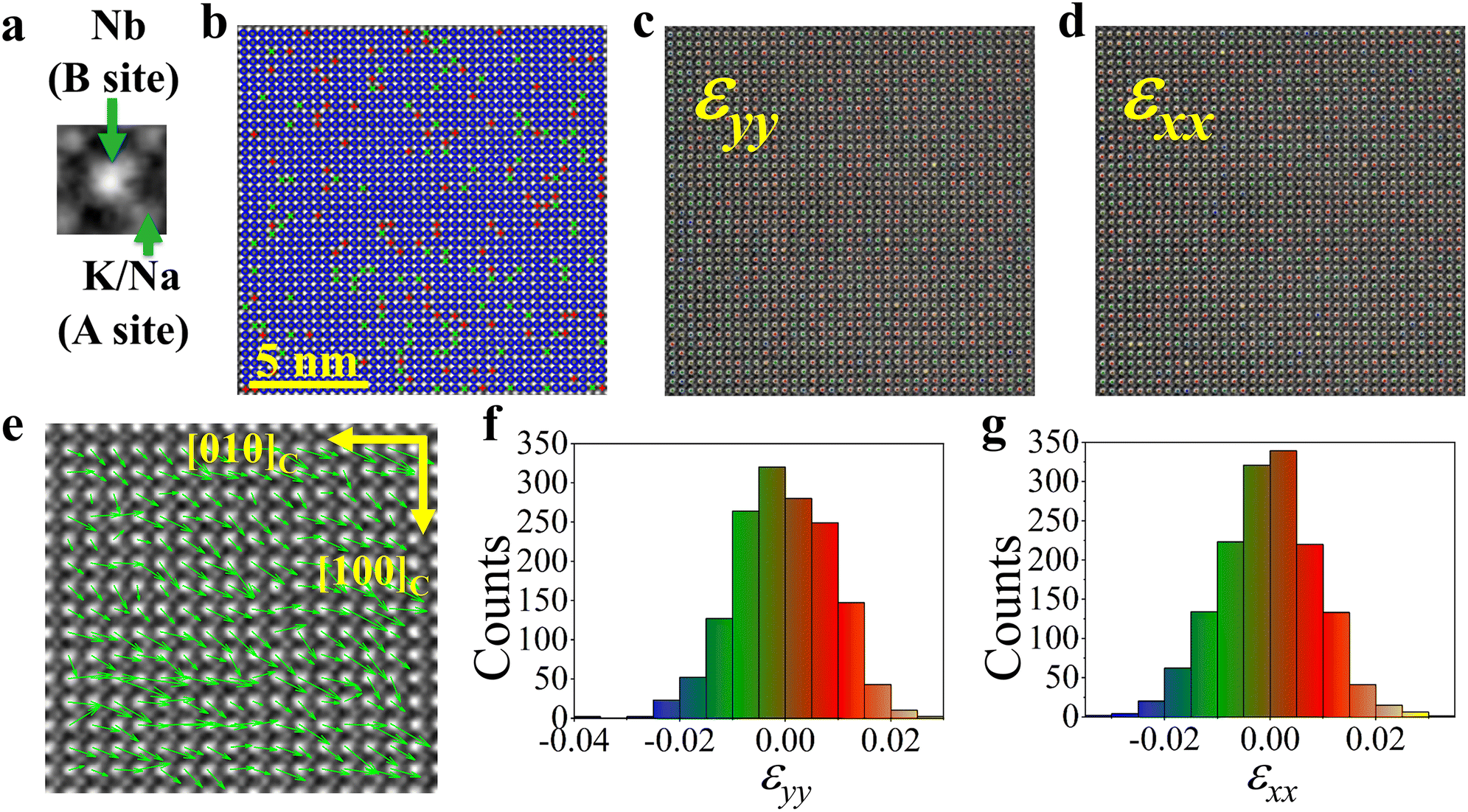 | ||
| Fig. 4 Analysis of HAADF-STEM for composition fluctuations, strain fluctuations, and polarization rotation. (a) Unit-cell of KNN. (b) A site intensity map. Atomic columns with higher intensity are K atoms dominated and denoted by green “×”. Atomic columns with lower A site intensity are Na atoms dominated and labeled by red “+”. Atomic columns with moderate intensity indicate relatively uniform distribution and are marked by blue “○”. (c and d) Strain maps analyzed with PPA. Colorful spots indicate the magnitudes of strain in the related unit-cell, while the blue and yellow indicate large strains (>|±2%|). Strain maps show distinct strain fluctuations. (e) Polarization vector map. Green vectors indicate the orientation and the magnitude of polarization of each unit-cell. Vector map displays polarization rotations by different degrees. (f and g) Statistics of strains for unit-cells. | ||
The strain in the compositionally graded KNN single crystal is different from the gradient strain caused by lattice mismatch between the film and substrate. The strain map of the HAADF-STEM image (Fig. 4c and d) through using Peak Pairs Analysis displays evident strain fluctuation different from the gradient strain case in the epitaxially grown film. Great strains (>|±2%|) larger than the average of all unit-cells exist in both εyy and εxx, as shown in Fig. 4f and g, and those in εxy and εyx are shown in Fig. S4.† The strain fluctuation may be caused by the compositional fluctuation at the atomic scale.
Atomic displacements of the Nb cation from the center of its four nearest neighboring K/Na cations represent the polarization vectors for each unit-cell. According to the determination of atomic position by the multiple-ellipse fitting method, the obtained polarization vectors are shown in Fig. 4e. Although the HAADF image is acquired in the one domain, the orientation of the polarization vector of each unit-cell is inconsistent. Some polarizations are rotated away from the [10], approaching [00] and even [0].
Generally, non-180° ferroelectric domain switching is a one-time effect during electrical poling. What is more interesting is that the KNN single crystals exhibit reversible domain switching under the action of the electric field. The reversibility of the domain indicates the existence of an inherent restoring force in the material. There are several possible origins of the restoring force in piezoelectrics, such as the symmetry-conforming properties of point defects,17 residual stress,19 and increased depolarization energy at a unique interface.20 However, those mechanisms cannot be used to explain the properties of undoped KNN single crystals. Therefore, the reversibility in the switching domain has a different source of restoring force. A previous report proposed a mechanism that a built-in flexoelectric effect can act as a restoring force in the KTN single crystal with compositional gradient.24 However, there has been no convincible direct evidence for the built-in flexoelectric effect in bulk materials.
As is well known, the flexoelectricity can force spontaneous polarization to rotate in ferroelectric thin films.31–33 However, few reports focused on bulk material with built-in flexoelectricity because of its small magnitude in bulk material. In our studies, the strain fluctuation is noticeable at the atomic scale, which can reduce the relaxation length of strain gradient in bulk material. The different values of strain between neighboring unit-cells can generate a strong flexoelectric effect. Consequently, the flexoelectric effect in the KNN single crystals is more robust than that in traditional bulk materials and causes polarization rotation. The rotated polarization consists of spontaneous polarization and flexoelectricity-induced polarization.
Contrary to homogeneous stress, the flexoelectric effect can be regarded as the electric field that causes the polarization orientation, and it can asymmetrically change the free energy distribution of equivalent spontaneous polarization and lower the energy barrier.32–34 Therefore, the existence of flexoelectricity will lead to the tendency of polarization orientation. We suggest that the restoring force in the KNN single crystals possibly derives from flexoelectricity. The flexoelectricity is caused by the fluctuation of the composition, which is unchangeable under the electric field. When the flexoelectric field is large enough to change and overcome the energy barrier between domains, the initial polarizations will deviate from the spontaneous polarization orientations to a great extent, and when the electric field is moved away, the polarization will rotate back to the initial polarization orientations. The strength of the flexoelectric field is crucial to reversible non-180° domain switching in crystals. Fig. 3h shows the reversibility ranging from 31% for (A4 + A5) to 91% for A3. This indicates that the strength of the flexoelectric field is nonuniform in the whole compositionally graded KNN single crystal. Therefore, due to the inhomogeneous distribution of the flexoelectric field, not all specimens present the reversibility of domain switching under an electric field in our in situ TEM experiments.
Conclusions
In summary, the reversible domain wall motion and the non-180° domain switching in compositionally graded KNN single crystals have been studied by in situ transmission electron microscopy using an electric field-available sample holder. At a small electric voltage, domain walls remain steady until electric voltage exceeds the coercive voltage. With the further increase of the electric field, the domain switching becomes more drastic. Conversely, with the decrease of the electric field, the reversed movements of domain walls are smoother and more uniform. The strength of reversibility is not uniform, which is caused by the different strengths of restoring force. For the compositionally graded KNN single crystal, the composition gradient is inconspicuous, while the composition fluctuation is significant at the atomic scale. The local compositional fluctuation leads to strain fluctuation at the atomic scale, and the strains of some unit-cells may exceed |±2%|. The strain fluctuation generates a significant strain gradient between neighboring unit-cells, subsequently leading to a tremendous flexoelectric field in the crystal. The flexoelectric effect can be regarded as an electric field that can affect the polarization orientation and modify the free energy profile of equivalent polarization orientation asymmetrically. We suggest that the flexoelectric effect is the origin of restoring force in the crystals. The strong built-in flexoelectric effect found in bulk material and the new mechanism of generating restoring force pave the way for improving the piezoelectric properties and the new performance of bulk material.Author contributions
R. Y. conceived and supervised the project. X. S. and Q. G. performed in situ TEM and STEM experiments. C. H., H. T., and Z. Z. grew the crystal samples. Q. G. prepared the TEM specimens by FIB. Q. G., X. L., and H. Z. analyzed the positions of atomic columns and polarizations. Q. G., Y. M., L. W., and Y. Y. analyzed the strains in the samples by PPA. Q. G., X. S., Z. Z., and R. Y. wrote the manuscript, and all authors amended the manuscript.Conflicts of interest
There are no conflicts to declare.Acknowledgements
This work was supported by the National Key Research Program of China (Grant No. 2022YFA1402801 and 2018YFA0208402), the National Natural Science Foundation of China (Grant No. 11874413, 11934017, 51972333, and 12074092) and the Strategic Priority Research Program of the Chinese Academy of Sciences (Grant No. XDB33030200). X. Shen is grateful for the support from the Youth Innovation Promotion Association of the Chinese Academy of Sciences (2019009).Notes and references
- H. Jaffe and D. A. Berlincourt, Proc. IEEE, 1965, 53, 1372–1386 Search PubMed.
- H.-C. Thong, C. Zhao, Z. Zhou, C.-F. Wu, Y.-X. Liu, Z.-Z. Du, J.-F. Li, W. Gong and K. Wang, Mater. Today, 2019, 29, 37–48 CrossRef CAS.
- J. Roedel, K. G. Webber, R. Dittmer, W. Jo, M. Kimura and D. Damjanovic, J. Eur. Ceram. Soc., 2015, 35, 1659–1681 CrossRef CAS.
- G. Lockitch, Clin. Biochem., 1993, 26, 371–381 CrossRef CAS PubMed.
- L. Egerton and D. M. Dillon, J. Am. Ceram. Soc., 1959, 42, 438–442 CrossRef CAS.
- Y. Saito, H. Takao, T. Tani, T. Nonoyama, K. Takatori, T. Homma, T. Nagaya and M. Nakamura, Nature, 2004, 432, 84–87 CrossRef CAS PubMed.
- X. Wang, J. Wu, D. Xiao, J. Zhu, X. Cheng, T. Zheng, B. Zhang, X. Lou and X. Wang, J. Am. Chem. Soc., 2014, 136, 2905–2910 CrossRef CAS PubMed.
- B. Wu, H. Wu, J. Wu, D. Xiao, J. Zhu and S. J. Pennycook, J. Am. Chem. Soc., 2016, 138, 15459–15464 CrossRef CAS PubMed.
- K. Xu, J. Li, X. Lv, J. Wu, X. Zhang, D. Xiao and J. Zhu, Adv. Mater., 2016, 28, 8519–8523 CrossRef CAS PubMed.
- H. Tao, H. Wu, Y. Liu, Y. Zhang, J. Wu, F. Li, X. Lyu, C. Zhao, D. Xiao, J. Zhu and S. J. Pennycook, J. Am. Chem. Soc., 2019, 141, 13987–13994 CrossRef CAS PubMed.
- Q. Liu, Y. Zhang, J. Gao, Z. Zhou, D. Yang, K. Y. Lee, A. Studer, M. Hinterstein, K. Wang, X. Zhang, L. Li and J. F. Li, Natl. Sci. Rev., 2020, 7, 355–365 CrossRef CAS PubMed.
- X. Lv, X.-x. Zhang and J. Wu, J. Mater. Chem. A, 2020, 8, 10026–10073 RSC.
- X. Gao, Z. Cheng, Z. Chen, Y. Liu, X. Meng, X. Zhang, J. Wang, Q. Guo, B. Li, H. Sun, Q. Gu, H. Hao, Q. Shen, J. Wu, X. Liao, S. P. Ringer, H. Liu, L. Zhang, W. Chen, F. Li and S. Zhang, Nat. Commun., 2021, 12, 881 CrossRef CAS PubMed.
- X. Lv and J. Wu, J. Mater. Chem. C, 2019, 7, 2037–2048 RSC.
- X. Liu and X. Tan, Adv. Mater., 2016, 28, 574–578 CrossRef CAS PubMed.
- M. H. Zhang, C. Shen, C. Zhao, M. Dai, F. Z. Yao, B. Wu, J. Ma, H. Nan, D. Wang, Q. Yuan, L. L. da Silva, L. Fulanovic, A. Schokel, P. Liu, H. Zhang, J. F. Li, N. Zhang, K. Wang, J. Rodel and M. Hinterstein, Nat. Commun., 2022, 13, 3434 CrossRef CAS PubMed.
- X. Ren, Nat. Mater., 2004, 3, 91–94 CrossRef CAS PubMed.
- L. X. Zhang and X. Ren, Phys. Rev. B: Condens. Matter Mater. Phys., 2005, 71, 174108 CrossRef.
- N. H. Khansur, H. Kawashima, S. Wada, J. M. Hudspeth and J. Daniels, Acta Mater., 2015, 98, 182–189 CrossRef CAS.
- M.-H. Zhang, Q. Zhang, T.-T. Yu, G. Li, H.-C. Thong, L.-Y. Peng, L. Liu, J. Ma, Y. Shen, Z. Shen, J. Daniels, L. Gu, B. Han, L.-Q. Chen, J.-F. Li, F. Li and K. Wang, Mater. Today, 2021, 46, 44–53 CrossRef CAS.
- C. Hu, X. Meng, M.-H. Zhang, H. Tian, J. E. Daniels, P. Tan, F. Huang, L. Li, K. Wang, J.-F. Li, Q. Lu, W. Cao and Z. Zhou, Sci. Adv., 2020, 6, eaay5979 CrossRef CAS PubMed.
- M. Davis, D. Damjanovic and N. Setter, J. Appl. Phys., 2004, 95, 5679–5684 CrossRef CAS.
- S. M. Kogan, Soviet Physics-Solid State, 1964, 5, 2069–2070 Search PubMed.
- F. Huang, C. P. Hu, Z. X. Zhou, X. D. Meng, P. Tan, Y. Wang, C. Z. Wang and H. Tian, Acta Mater., 2020, 200, 24–34 CrossRef CAS.
- P. Zubko, G. Catalan and A. K. Tagantsev, Annu. Rev. Mater. Res., 2013, 43, 387–421 CrossRef CAS.
- P. L. Galindo, S. Kret, A. M. Sanchez, J. Y. Laval, A. Yanez, J. Pizarro, E. Guerrero, T. Ben and S. I. Molina, Ultramicroscopy, 2007, 107, 1186–1193 CrossRef CAS PubMed.
- L. A. Schmitt, D. Schrade, H. Kungl, B.-X. Xu, R. Mueller, M. J. Hoffmann, H.-J. Kleebe and H. Fuess, Comput. Mater. Sci., 2014, 81, 123–132 CrossRef CAS.
- J. Fousek and V. Janovec, J. Appl. Phys., 1969, 40, 135–142 CrossRef CAS.
- J. Fousek, Czech J. Phys. B, 1971, 21, 955–968 CrossRef CAS.
- S. Wada, K. Muraoka, H. Kakemoto, T. Tsurumi and H. Kumagai, Mater. Sci. Eng., B, 2005, 120, 186–189 CrossRef.
- G. Catalan, A. Lubk, A. H. Vlooswijk, E. Snoeck, C. Magen, A. Janssens, G. Rispens, G. Rijnders, D. H. Blank and B. Noheda, Nat. Mater., 2011, 10, 963–967 CrossRef CAS PubMed.
- Y. Gu, Z. Hong, J. Britson and L.-Q. Chen, Appl. Phys. Lett., 2015, 106, 022904 CrossRef.
- Y. Cao, L.-Q. Chen and S. V. Kalinin, Appl. Phys. Lett., 2017, 110, 202903 CrossRef.
- H. Lu, C. W. Bark, D. Esque de los Ojos, J. Alcala, C. B. Eom, G. Catalan and A. Gruverman, Science, 2012, 336, 59–61 CrossRef CAS PubMed.
Footnote |
| † Electronic supplementary information (ESI) available. See DOI: https://doi.org/10.1039/d3ta00737e |
| This journal is © The Royal Society of Chemistry 2023 |